JP4738536B1 - Nonvolatile memory controller and nonvolatile memory control method - Google Patents
Nonvolatile memory controller and nonvolatile memory control methodDownload PDFInfo
- Publication number
- JP4738536B1 JP4738536B1JP2010019223AJP2010019223AJP4738536B1JP 4738536 B1JP4738536 B1JP 4738536B1JP 2010019223 AJP2010019223 AJP 2010019223AJP 2010019223 AJP2010019223 AJP 2010019223AJP 4738536 B1JP4738536 B1JP 4738536B1
- Authority
- JP
- Japan
- Prior art keywords
- data
- page
- management table
- written
- valid
- Prior art date
- Legal status (The legal status is an assumption and is not a legal conclusion. Google has not performed a legal analysis and makes no representation as to the accuracy of the status listed.)
- Expired - Fee Related
Links
Images


Classifications
- G—PHYSICS
- G06—COMPUTING OR CALCULATING; COUNTING
- G06F—ELECTRIC DIGITAL DATA PROCESSING
- G06F12/00—Accessing, addressing or allocating within memory systems or architectures
- G06F12/02—Addressing or allocation; Relocation
- G06F12/08—Addressing or allocation; Relocation in hierarchically structured memory systems, e.g. virtual memory systems
- G06F12/10—Address translation
- G—PHYSICS
- G06—COMPUTING OR CALCULATING; COUNTING
- G06F—ELECTRIC DIGITAL DATA PROCESSING
- G06F12/00—Accessing, addressing or allocating within memory systems or architectures
- G06F12/02—Addressing or allocation; Relocation
- G06F12/0223—User address space allocation, e.g. contiguous or non contiguous base addressing
- G06F12/023—Free address space management
- G06F12/0238—Memory management in non-volatile memory, e.g. resistive RAM or ferroelectric memory
- G06F12/0246—Memory management in non-volatile memory, e.g. resistive RAM or ferroelectric memory in block erasable memory, e.g. flash memory
- G—PHYSICS
- G06—COMPUTING OR CALCULATING; COUNTING
- G06F—ELECTRIC DIGITAL DATA PROCESSING
- G06F3/00—Input arrangements for transferring data to be processed into a form capable of being handled by the computer; Output arrangements for transferring data from processing unit to output unit, e.g. interface arrangements
- G06F3/06—Digital input from, or digital output to, record carriers, e.g. RAID, emulated record carriers or networked record carriers
- G06F3/0601—Interfaces specially adapted for storage systems
- G06F3/0628—Interfaces specially adapted for storage systems making use of a particular technique
- G06F3/0638—Organizing or formatting or addressing of data
- G06F3/064—Management of blocks
- G—PHYSICS
- G06—COMPUTING OR CALCULATING; COUNTING
- G06F—ELECTRIC DIGITAL DATA PROCESSING
- G06F3/00—Input arrangements for transferring data to be processed into a form capable of being handled by the computer; Output arrangements for transferring data from processing unit to output unit, e.g. interface arrangements
- G06F3/06—Digital input from, or digital output to, record carriers, e.g. RAID, emulated record carriers or networked record carriers
- G06F3/0601—Interfaces specially adapted for storage systems
- G06F3/0668—Interfaces specially adapted for storage systems adopting a particular infrastructure
- G06F3/0671—In-line storage system
- G06F3/0673—Single storage device
- G06F3/0679—Non-volatile semiconductor memory device, e.g. flash memory, one time programmable memory [OTP]
- G—PHYSICS
- G06—COMPUTING OR CALCULATING; COUNTING
- G06F—ELECTRIC DIGITAL DATA PROCESSING
- G06F2212/00—Indexing scheme relating to accessing, addressing or allocation within memory systems or architectures
- G06F2212/72—Details relating to flash memory management
- G06F2212/7201—Logical to physical mapping or translation of blocks or pages
- G—PHYSICS
- G06—COMPUTING OR CALCULATING; COUNTING
- G06F—ELECTRIC DIGITAL DATA PROCESSING
- G06F2212/00—Indexing scheme relating to accessing, addressing or allocation within memory systems or architectures
- G06F2212/72—Details relating to flash memory management
- G06F2212/7205—Cleaning, compaction, garbage collection, erase control
Landscapes
- Engineering & Computer Science (AREA)
- Theoretical Computer Science (AREA)
- Physics & Mathematics (AREA)
- General Engineering & Computer Science (AREA)
- General Physics & Mathematics (AREA)
- Human Computer Interaction (AREA)
- Memory System (AREA)
- Techniques For Improving Reliability Of Storages (AREA)
Abstract
Translated fromJapaneseDescription
Translated fromJapanese本発明はフラッシュメモリ等の不揮発性メモリのコントローラ及び不揮発性メモリの制御方法に関する。 The present invention relates to a controller for a nonvolatile memory such as a flash memory and a method for controlling the nonvolatile memory.
一般に不揮発性メモリ、例えばフラッシュメモリはデータの書き込みおよび削除の際に既存データを残したまま別の物理領域へ書き込みを行うため、データの書き込みや削除を繰り返すと、分断された不要な領域が削除されずに残り、使用している領域も非連続的に保持されている。この不要な領域を消去し、使用している領域を連続した領域に纏める処理はコンパクション、あるいはガーベジコレクションと呼ばれる。従来の半導体記憶装置のガーベジコレクション処理は例えば、特許文献1に記載されている。 In general, non-volatile memory, for example flash memory, writes to another physical area while leaving existing data at the time of data writing and deletion, so when repeated data writing and deletion, the divided unnecessary area is deleted The area that is used and is being used is also held discontinuously. The process of erasing unnecessary areas and collecting used areas into a continuous area is called compaction or garbage collection. A conventional garbage collection process of a semiconductor memory device is described in Patent Document 1, for example.
データ書き込み処理あるいは無効化処理の後、管理データの更新を行い、フラッシュメモリ内の領域使用率を計算する。領域使用率の計算の結果に応じてガーベジコレクションの必要があるか否かを判断し、必要があればガーベジコレクションを行う。ガーベジコレクション処理は比較的時間が長いため、ガーベジコレクション処理と同時にユーザデータクセスを実行すると、ユーザデータクセス時間が通常状態時よりも遅くなってしまう欠点がある。この問題はフラッシュメモリのユーザデータクセス処理とガーベジコレクション処理を異なるタイミングで実行させることにより解決できる。そのため、特許文献1記載の装置は、ガーベジコレクションのような不要なデータを消去するタイミングを外部に通知可能なフラッシュメモリを提供する手段を具備する。比率計算部はフラグ領域の状態を判定して、ユーザ領域の状態を判定してユーザ領域が無効である比率を算出し、算出した比率を制御部に送る。制御部は比率を受信し、データの書き込み動作または無効化処理の直後に外部に出力する。フラッシュメモリの制御部は書き込み命令を受け取ると、指定されたユーザ領域にデータを書き込む。さらに、対応するフラグ領域に、データが有効であることを示す値を書き込む。その後、比率計算部で、フラグ領域の状態を判定して、ユーザ領域が無効である比率を算出させる。比率計算部で算出された比率を受け取り、これをデータバスに出力して外部に通知する。 After the data write process or invalidation process, the management data is updated and the area usage rate in the flash memory is calculated. It is determined whether or not garbage collection is necessary according to the calculation result of the area usage rate. If necessary, garbage collection is performed. Since the garbage collection process takes a relatively long time, if user data access is executed at the same time as the garbage collection process, there is a drawback that the user data access time becomes slower than in the normal state. This problem can be solved by executing the flash memory user data access process and the garbage collection process at different timings. For this reason, the apparatus described in Patent Document 1 includes means for providing a flash memory that can notify the timing of erasing unnecessary data such as garbage collection to the outside. The ratio calculation unit determines the state of the flag area, determines the state of the user area, calculates the ratio that the user area is invalid, and sends the calculated ratio to the control unit. The control unit receives the ratio and outputs it to the outside immediately after the data write operation or invalidation process. When the control unit of the flash memory receives the write command, it writes data in the designated user area. Further, a value indicating that the data is valid is written in the corresponding flag area. Thereafter, the ratio calculation unit determines the state of the flag area and calculates the ratio that the user area is invalid. The ratio calculated by the ratio calculation unit is received and output to the data bus to notify the outside.
上記した問題以外にもガーベジコレクション処理による動作速度の低下の要因がある。ガーベジコレクション処理の準備のために、ファームウェアはハードウェアに対して、ガーベジコレクションの対象候補となるブロックの検索動作の要求を定期的もしくは一意に実施する必要がある。 In addition to the above problems, there is a factor of a decrease in operation speed due to the garbage collection process. In preparation for the garbage collection process, the firmware needs to periodically or uniquely perform a request for a search operation for blocks that are candidates for garbage collection to the hardware.
従来、該検索のために一時的にメインメモリへのアクセスが増加し、メインメモリの転送帯域を消費してしまうことがあり、フラッシュメモリとメインメモリとの間のユーザデータ転送に係るメインメモリアクセスが阻害され、結果としてユーザから見た速度性能が劣化する場合があった。 Conventionally, access to the main memory temporarily increases due to the search, and the transfer bandwidth of the main memory may be consumed. Main memory access related to user data transfer between the flash memory and the main memory As a result, the speed performance viewed from the user may deteriorate.
特許文献1記載の半導体記憶装置では、チップ内部の有効ブロック数を判断するために使用する「フラグ領域」と呼ばれるテーブル情報を、フラッシュメモリチップメモリセル部に記憶している。ガーベジコレクション候補を検索する際に必ず該テーブルをアクセス(フラッシュメモリへのアクセス)しなければならない。フラッシュメモリチップ単体でガーベジコレクション候補ブロックを判定する方式のため、チップ毎にガーベジコレクションを実施できる。 In the semiconductor memory device described in Patent Document 1, table information called “flag area” used for determining the number of effective blocks in a chip is stored in a flash memory chip memory cell unit. When searching for garbage collection candidates, the table must be accessed (access to the flash memory). Since the flash memory chip alone determines a garbage collection candidate block, garbage collection can be performed for each chip.
従来の不揮発性メモリのコントローラは、コンパクションの対象候補となるブロックの検索動作によりメインメモリへのアクセス速度が低下するという課題がある。 The conventional nonvolatile memory controller has a problem that the access speed to the main memory decreases due to the search operation for the block that is a candidate for compaction.
本発明はコンパクション処理の対象候補となるブロックの検索動作がメインメモリへのアクセス速度に影響しない不揮発性メモリのコントローラ及び不揮発性メモリの制御方法を提供することを目的とする。 It is an object of the present invention to provide a non-volatile memory controller and a non-volatile memory control method in which a search operation for blocks that are candidates for compaction processing does not affect the access speed to the main memory.
本発明の一態様による不揮発性メモリのコントローラは、不揮発性メモリへのデータ書き込み時にデータ書き込みに伴い無効にすべきページが属するブロックの有効ページ数をカウントするカウント手段と、カウント手段によりカウントされた有効ページ数が所定数以下の場合、前記ブロックをコンパクション処理の対象とする追加手段とを具備する。 The controller of the nonvolatile memory according to one aspect of the present invention is configured to count a valid page of a block to which a page to be invalidated along with data writing belongs when the data is written to the nonvolatile memory. When the number of valid pages is equal to or less than a predetermined number, the image processing apparatus includes an adding unit that targets the block for compaction processing.
本発明の他の態様による不揮発性メモリの制御方法は、ライト対象の論理ブロックアドレスを物理ブロックアドレスに変換して不揮発性メモリへデータを書き込むことと、前記不揮発性メモリへのデータ書き込みが終了すると、一定バイトからなるページ毎に不揮発性メモリのデータの有効、無効を管理する有効ページ管理テーブルを更新することと、前記更新された有効ページ管理テーブルに基づいて、前記ライト対象の論理ブロックアドレスに対応し以前にデータが書き込まれた旧物理ブロックの有効ページ数をカウントすることと、カウントした前記有効ページ数が所定数以下の場合、前記旧物理ブロックのアドレスを、所定ページからなるブロック毎にコンパクション処理の候補を管理するコンパクション候補管理テーブルに追加することとを具備する。 According to another aspect of the present invention, there is provided a non-volatile memory control method that converts a logical block address to be written into a physical block address, writes data to the non-volatile memory, and finishes writing data to the non-volatile memory. Updating the valid page management table for managing the validity / invalidity of the data in the nonvolatile memory for each page consisting of a certain number of bytes and, based on the updated valid page management table, to the logical block address to be written Correspondingly, the number of valid pages of the old physical block to which data has been previously written is counted, and when the counted number of valid pages is less than or equal to a predetermined number, the address of the old physical block is set for each block consisting of a predetermined page. Add to the compaction candidate management table for managing compaction processing candidates ; And a thing.
本発明の一態様によれば、通常のデータ書き込み動作に付随してコンパクション候補検索の一部とコンパクション候補設定が自動的に実行される。このため、従来のファームウェアが必要としていた定期的なコンパクションの対象候補となるブロックの検索動作の要求を不要とすることができる。このようにファームウェアによって起動される検索動作の回数を低減させることによって、一時的に増加するメインメモリの帯域消費の比率が低下し、NAND型フラッシュメモリとのユーザデータ転送に係るメインメモリへのアクセスが阻害されにくくなるため、その分速度性能劣化を防止できる。 According to one aspect of the present invention, a part of compaction candidate search and compaction candidate setting are automatically executed in association with a normal data writing operation. For this reason, it is possible to eliminate the need for a search operation for a block that is a candidate for periodic compaction, which is required by conventional firmware. By reducing the number of search operations started by the firmware in this way, the ratio of bandwidth consumption of the main memory that temporarily increases is reduced, and access to the main memory related to user data transfer with the NAND flash memory is reduced. Is less likely to be hindered, and accordingly, speed performance deterioration can be prevented.
以下、図面を参照して本発明の実施の形態について詳細に説明する。 Hereinafter, embodiments of the present invention will be described in detail with reference to the drawings.
図1は一実施形態の構成を示すブロック図である。本実施形態は複数の不揮発性メモリ、例えばNAND型フラッシュメモリ81、82、…8nを含む。NAND型フラッシュメモリ81、82、…8nは例えば半導体ドライブ(Solid State Drive: SSD)の記憶部を構成する。NAND型フラッシュメモリ81、82…8nの各々は例えば2〜16個のメモリチップからなる。NAND型フラッシュメモリ81、82、…8nはNANDフラッシュメモリコントローラ1に接続される。NANDフラッシュメモリコントローラ1はメモリアクセスバス2bで互いに接続されたCPU2と、メインメモリ3と、NANDフラッシュメモリインターフェース(I/F)6とを具備する。NANDフラッシュメモリインターフェース(I/F)6はNAND型フラッシュメモリ81、82、…8nに接続され、NAND型フラッシュメモリ81、82、…8nへのアクセスを制御する。メインメモリ3は例えばdRAMからなり、ブロック内有効ページ管理ビットマップテーブル5とコンパクション候補管理テーブル4を含む。FIG. 1 is a block diagram showing a configuration of an embodiment. The present embodiment includes a plurality of nonvolatile memories, for example, NAND
NANDフラッシュメモリコントローラ1のメモリアクセスバス2bには外付けのROM9も接続される。ROM9はファームウェア7を含む。ファームウェア7はCPU2を使用し、NANDフラッシュメモリI/F6内部へのI/OコマンドアクセスによりNAND型フラッシュメモリ81、82、…8nへのリードコマンド、ライトコマンドの発行を行う。An external ROM 9 is also connected to the
NANDフラッシュメモリI/F6はCPU2からの命令を受理し、NAND型フラッシュメモリ81、82、…8nとメインメモリ3間のデータ転送を実施する。The NAND flash memory I /
ファームウェア7はROM9にプログラムされた内容が、システム電源起動時に、CPU2内部の一時記憶部もしくはメインメモリ3に転送されて動作するものとする。ファームウェア7からのNAND型フラッシュメモリ81、82、…8nアクセス操作は論理ブロックアドレス(LBA: Logical Block Address)を用いて実施される。The
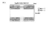
ブロック内有効ページ管理ビットマップテーブル5は、図2に示すように構成されている。NAND型フラッシュメモリ81、82、…8nの各ページが有効(Valid)か無効(Invalid)かを示すためのビットマップ構成をとる。所定のバイト、例えば2112バイト毎に1ページを構成し、所定のページ、例えば64ページが1ブロックを構成する。有効とは、当該ページ内に書き込まれたデータが存在し、そのデータは有効であることを示している。無効とは、当該ページ内に何も書き込まれていないか、もしくは当該ページ内に以前書き込まれていたデータが無効になった場合(同一LBAの最新データが書き込まれた場合)を示している。The intra-block valid page management bitmap table 5 is configured as shown in FIG. The NAND
ブロック内有効ページ管理ビットマップテーブル5はNAND型フラッシュメモリ81、82、…8nへの書き込みが発生すると、有効/無効状態が更新される。ファームウェア7からの書き込み操作はLBAを用いて実施される。従って、NAND型フラッシュメモリ81、82、…8nに対して実際に書き込む場合は、LBAを物理アドレス(ブロックアドレス、ページアドレス)に変換して、データが書き込まれる。The valid / invalid state of the intra-block valid page management bitmap table 5 is updated when writing to the
NAND型フラッシュメモリ81、82、…8nは同一セルへの書き込みを実施すると特性上、内部セルの寿命が極端に低下する。それを防ぐため、ファームウェア7とNANDフラッシュメモリI/F6は同じLBAでデータを複数回書き込む場合でも、以前書き込んだ物理アドレスとは異なる物理アドレスのページにデータを新規に書き込み、以前書き込んだ物理アドレスのページに格納されているデータを無効とする処理を行う。この有効/無効管理を実施するためにブロック内有効ページ管理ビットマップテーブル5が存在している。従って、このような書き込み操作を実施しながらシステムが動作しているうちに、いずれは有効ページ数の少ないブロック(すなわち、コンパクション処理の対象となるブロック)が発生してくるのは必須である。When the
従来、ファームウェア7はブロック内有効ページ数を一意にカウントし、有効数がある一定数以下であれば、そのブロックをコンパクション対象の一つとしてエントリし、コンパクション処理に適用していた。コンパクション処理とは、複数のブロック内の有効ページデータをかき集めて、別のブロックに移動させ、移動元のページを無効化し、何も書かれていない空きブロックを作り出す操作のことであり、コンパクション候補管理テーブル4はそのために存在する。 Conventionally, the
コンパクションの候補となるブロックは複数種類あり、有効ページ比率が低くなったブロック、エラーが頻発するブロック、リードのみを規定回数実施したブロックなどが挙げられる。本実施形態はこの中で有効ページ比率が低下した時のコンパクション処理に関し、その候補の検索を効率化するためのものである。 There are a plurality of types of blocks that are candidates for compaction, such as a block with a low effective page ratio, a block with frequent errors, and a block that has been read only a specified number of times. The present embodiment relates to the compaction process when the effective page ratio is lowered, and is to improve the search for the candidate.
従来、ブロック内有効ページ管理ビットマップテーブル5のブロック内有効ページ数のカウントには専用のハードウェアが用いられ、ファームウェア7は定期的、もしくは一意に該ハードウェアを動作させてコンパクション候補を検索特定し、コンパクション候補管理テーブル4に追加していた。そのため、検索動作に必要なメインメモリ3へのアクセスが一時的に集中することがあり、NAND型フラッシュメモリ81、82、…8nとのデータ転送に必要なメモリアクセスを阻害し、ユーザに対するデータ提供速度性能を劣化させる事があった。Conventionally, dedicated hardware is used to count the number of valid pages in a block in the intra-block valid page management bitmap table 5, and the
本実施形態ではデータ書き込み動作終了時にブロック内有効ページ管理ビットマップテーブル5の更新を行うと同時に、無効化する側(同じLBAで以前に書き込んだ物理ブロック)のブロック内有効ページ数カウントを実施し、設定数以下であった場合、以前に書き込んだ物理ブロックをコンパクション候補としてコンパクション候補管理テーブル4に追加する。ファームウェア7が起動するコンパクション候補検索は、コンパクション候補管理テーブル4が保持している候補がある一定量を切った場合に発生する可能性がある。しかし、本実施形態では、データ書き込み動作終了時にハードウェアによってある程度自動的にコンパクション候補管理テーブル4に候補を追加することが可能になるので、ファームウェア7が起動するコンパクション候補の検索動作要求の回数を低減させることができる。そのため、コンパクション候補検索のためのメインメモリ3へのアクセスの集中が緩和され、NAND型フラッシュメモリ8とメインメモリ3との間のユーザデータ転送のためのメインメモリ3へのアクセスが阻害されにくくなり、速度性能劣化を低減することができる。 In this embodiment, at the end of the data write operation, the in-block valid page management bitmap table 5 is updated, and at the same time, the number of in-block valid pages is counted on the invalidation side (physical block previously written with the same LBA) If the number is less than the set number, the previously written physical block is added to the compaction candidate management table 4 as a compaction candidate. The compaction candidate search activated by the
図3はコンパクション候補管理テーブル4とNAND型フラッシュメモリ81、82、…8n内の該当ブロックとの関係を示す図である。コンパクション候補管理テーブル4は主にファームウェア7が管理しており、図の例ではキュー(FIFO)構造を想定している。従って、NAND型フラッシュメモリ81、82、…8n内の物理ブロックアドレス(physical block address)の先頭値をキューのデータとし、リードポインタ(RP)とライトポインタ(WP)をそれぞれ具備している。キューへの書き込みはライトポインタが示すアドレスに対して実施し、コンパクションを実行する場合の対象ブロックアドレスはリードポインタをアドレスとしたキューに保持された物理ブロックアドレスが使用される。各々ポインタ操作については一般的なキュー操作方法と同等である。FIG. 3 is a diagram showing the relationship between the compaction candidate management table 4 and the corresponding blocks in the
図4はNANDフラッシュメモリI/F6の詳細なブロック図である。メモリアクセスバス2bはCPU2からNANDフラッシュメモリI/F6をアクセスしたり、NANDフラッシュメモリI/F6からメインメモリ3をアクセスするために使用する内部バスである。 FIG. 4 is a detailed block diagram of the NAND flash memory I /
NAND型フラッシュメモリ8へのアクセスはI/Oバッファ57を経由して行われる。メモリアクセスバス2bからのライトデータはデータバッファ52、データプロセッサ53を介してI/Oバッファ57に供給され、I/Oバッファ57からのリードデータはデータプロセッサ53、データバッファ52を介してメモリアクセスバス2bに供給される。I/Oバッファ57とNAND型フラッシュメモリ8とはデータ/ステータスと、コマンドにより接続される。 Access to the
CPU2からのリードコマンド、ライトコマンドはメモリアクセスバス2bを介してコマンドキュー54に書き込まれる(ファームウェアによりプッシュされる)。ここでのコマンドフォーマットはNANDフラッシュメモリI/F6が処理しやすいビットフォーマットであればよく、ハードウェア実装に依存している。コマンドキュー54にコマンドが書き込まれると、コマンドプロセッサ55はエントリされたコマンドをコマンドキュー54から取り出し、コマンドシーケンサ56にコマンドを発行して起動をかける。 Read commands and write commands from the
コマンドシーケンサ56はNAND型フラッシュメモリ8のアクセスを実施する。コマンドシーケンサ56はNAND型フラッシュメモリ8のアクセスの際、データプロセッサ53に対してデータ転送要求を実施し、データプロセッサ53はデータ転送が完了するとコマンドシーケンサ56に終了レスポンスを返す。コマンドシーケンサ56は終了コマンドをコマンドプロセッサ55に通知すると、コマンドプロセッサ55はテーブル更新エンジン61に対して終了コマンドを送付する。 The
テーブル更新エンジン61は終了したコマンドに係るメインメモリ3上のテーブル更新を実施するモジュールであり、コンパクション候補ブロックの有効ページ数サーチ機能やライト終了時の有効ページ管理ビットマップテーブル5の更新処理及び、その他の管理テーブルの更新処理を実施する。本実施形態では本質に関係しないので、有効ページ管理ビットマップテーブル5の更新処理以外の更新処理の説明は省略する。テーブル更新エンジン61はすべての処理を終了後、リプライキュー62に終了コマンド情報をプッシュしてハードウェアとしてのコマンド処理が完了する。 The
ファームウェア7はリプライキュー62をリードすることによってコマンド実行結果を確認する。 The
レジスタモジュール59はNANDフラッシュメモリI/F6の各種設定レジスタモジュールであり、CPU2から種々のデータが設定される。レジスタモジュール59はページ有効サーチレジスタ60、コンパクションテーブルエントリライトポインタアドレスレジスタ64を含む。ページ有効サーチレジスタ60はテーブル更新エンジン61に対してライト終了時にページ有効カウントを実施するかどうかを決めるイネーブル(EN)およびコンパクション候補にする場合の有効数閾値(Threshold)を渡す。 The
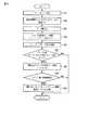
図5は一実施形態のライトに関する動作を示すフローチャートである。 FIG. 5 is a flowchart showing an operation related to writing according to an embodiment.
ブロック#12でライトコマンドを発行し、ブロック#14でライトコマンドの対象であるLBAを物理アドレス(ブロック/ページ)に変換する。物理アドレスに基づいてブロック#16でNAND型フラッシュメモリ81、82、…8nにデータを書き込む。データ書き込み動作が終了すると、ブロック#18でテーブル更新エンジン61はメインメモリ3に配置したブロック内有効ページ管理ビットマップテーブル5をリードする。ブロック#20でビットマップテーブル5を次のように更新する。すなわち、今回の書き込み対象である物理ブロック内の該当ページ部を有効にし、今回の書き込み対象である論理ブロックに対応する以前の書き込み対象の物理ブロックの該当ページ部を無効にする。In
ブロック#22でページ有効サーチレジスタ60のイネーブルがオンか否かを判定し、オンの場合、更新後のブロック内有効ページ管理ビットマップテーブル5に基づいて、ブロック#24で以前の書き込み対象の物理ブロックのページフィールド部の有効ページ数をカウントする。ブロック#26で、カウント値を有効数閾値(Threshold)と比較する。 In
カウント値が有効数閾値(Threshold)以下であった場合、すなわち旧書き込み対象の物理ブロックの有効ページ数が少ない場合、ブロック#28でコンパクション候補管理テーブル4に対して該ブロックをコンパクション候補として追加する。 When the count value is equal to or smaller than the effective number threshold (Threshold), that is, when the number of effective pages of the old write target physical block is small, the block is added as a compaction candidate to the compaction candidate management table 4 in
なお、上述したように、コンパクション候補管理テーブル4はキュー構造を採用しているので、テーブル4にエントリ(コンパクション候補として追加)するためにはテーブル4のライトポインタ情報をハードウェアが知らなければならない。そのため、そのアドレスを示すコンパクションテーブルエントリライトポインタアドレスレジスタ64をレジスタモジュール59に実装している。ライトポインタアドレスレジスタ64に設定されたアドレスを使用してライトポインタが格納されているメインメモリ3を直接アクセスしてライトポインタ情報を得ることができる。 As described above, since the compaction candidate management table 4 employs a queue structure, the hardware must know the write pointer information of the table 4 in order to enter (add as a compaction candidate) to the table 4. . Therefore, a compaction table entry write
以上説明したように、第1の実施の形態によれば、フラッシュメモリ81、812、…81nへのデータ書き込み修了時に、ブロック内有効ページ管理ビットマップテーブル5を更新し、更新後のブロック内有効ページ管理ビットマップテーブル5に基づいて、今回のライト対象の論理ブロックアドレスに対応し以前にデータが書き込まれた旧物理ブロックの有効ページ数をカウントする。カウントした有効ページ数が所定数以下の場合、旧物理ブロックをコンパクション候補としてコンパクション候補管理テーブル4に追加する。As described above, according to the first embodiment, the
このため、通常のデータ書き込み動作に付随してコンパクション候補検索の一部とコンパクション候補設定が自動的に実行される。従って、従来のファームウェアが必要としていた定期的なコンパクションの対象候補となるブロックの検索動作の要求を不要とすることができる。このようにファームウェアによって起動される検索動作の回数を低減させることによって、一時的に増加するメインメモリの帯域消費の比率が低下し、NAND型フラッシュメモリとのユーザデータ転送に係るメインメモリへのアクセスが阻害されにくくなるため、その分速度性能劣化を防止できる。 For this reason, a part of the compaction candidate search and compaction candidate setting are automatically executed along with the normal data writing operation. Therefore, it is possible to eliminate the need for a search operation for a block that is a candidate for periodic compaction, which is required by conventional firmware. By reducing the number of search operations started by the firmware in this way, the ratio of bandwidth consumption of the main memory that temporarily increases is reduced, and access to the main memory related to user data transfer with the NAND flash memory is reduced. Is less likely to be hindered, and accordingly, speed performance deterioration can be prevented.
なお、この発明は、上記実施形態そのままに限定されるものではなく、実施段階ではその要旨を逸脱しない範囲で構成要素を変形して具体化できる。また、上記実施形態に開示されている複数の構成要素の適宜な組み合せにより種々の発明を形成できる。例えば、実施形態に示される全構成要素から幾つかの構成要素を削除してもよい。更に、異なる実施形態に亘る構成要素を適宜組み合せてもよい。例えば、コンパクション候補管理テーブル4はキュー構造で限定されない。例えば、データチェーン構造をとっていた場合は、チェーンの最終データが保持しているポインタのアドレスに対して、コンパクション候補データのエントリ追加をすればよい。 Note that the present invention is not limited to the above-described embodiment as it is, and can be embodied by modifying the constituent elements without departing from the scope of the invention in the implementation stage. Further, various inventions can be formed by appropriately combining a plurality of constituent elements disclosed in the embodiment. For example, some components may be deleted from all the components shown in the embodiment. Furthermore, you may combine suitably the component covering different embodiment. For example, the compaction candidate management table 4 is not limited to a queue structure. For example, when the data chain structure is adopted, an entry of compaction candidate data may be added to the address of the pointer held by the final data of the chain.
本発明はNANDフラッシュメモリコントローラ1を使用するシステムであれば、どのようなシステムにも適用可能である。例えば、半導体ドライブ(Solid State Drive: SSD)と呼ばれる機器や、シリコンオーディオ機器、メモリメディアカードなどに適用することができるが、その際には実施例で示した構成の他に、システム特有のホストバスを追加する必要がある。SSDであれば、SAS/SATAのホストバスインターフェース等を追加する必要がある。 The present invention is applicable to any system that uses the NAND flash memory controller 1. For example, the present invention can be applied to a device called a solid state drive (SSD), a silicon audio device, a memory media card, etc. In this case, in addition to the configuration shown in the embodiment, a host specific to the system is used. It is necessary to add a bus. In the case of SSD, it is necessary to add a SAS / SATA host bus interface or the like.
また、本発明は、コンピュータに所定の手段を実行させるため、コンピュータを所定の手段として機能させるため、コンピュータに所定の機能を実現させるため、あるいはプログラムを記録したコンピュータ読取り可能な記録媒体としても実施することもできる。 The present invention can also be implemented to cause a computer to execute predetermined means, to cause a computer to function as predetermined means, to cause a computer to realize predetermined functions, or as a computer-readable recording medium storing a program. You can also
また、上述の説明は個々の実施例それぞれについて行ったが、複数の実施例を適宜組み合わせてもよい。 Moreover, although the above-mentioned description was performed about each Example, you may combine several Example suitably.
1…NANDフラッシュメモリコントローラ、2…CPU、3…メインメモリ、4…コンパクション候補管理テーブル、5…ブロック内有効ページ管理ビットマップテーブル、6…NANDフラッシュメモリI/F、8…NAND型フラッシュメモリ、9…ROM。 DESCRIPTION OF SYMBOLS 1 ... NAND flash memory controller, 2 ... CPU, 3 ... Main memory, 4 ... Compaction candidate management table, 5 ... In-block effective page management bitmap table, 6 ... NAND flash memory I / F, 8 ... NAND flash memory, 9 ... ROM.
Claims (10)
Translated fromJapanese不揮発性メモリへのデータ書き込み時にデータ書き込みに伴い無効にすべきページが属するブロックの有効ページ数をカウントするカウント手段と、
前記カウント手段によりカウントされた有効ページ数が所定数以下の場合、前記ブロックをコンパクション処理の対象とする追加手段と、
を具備するコントローラ。A non-volatile memory controller,
Counting means for counting the number of valid pages of a block to which a page to be invalidated along with data writing at the time of data writing to the nonvolatile memory;
When the number of valid pages counted by the counting unit is a predetermined number or less, an adding unit that targets the block for compaction processing;
A controller comprising:
前記カウント手段はデータ書き込み時に、ライト対象の論理ブロックアドレスに対応して今回書き込みが行われたページを有効とし、該ライト対象の論理ブロックアドレスに対応して以前に書き込みが行われたページを無効とし、前記有効ページ管理テーブルを更新する請求項1記載のコントローラ。It further comprises an effective page management table for managing the validity / invalidity of the data in the nonvolatile memory for each page,
When the data is written, the counting means validates the page written this time corresponding to the logical block address to be written and invalidates the page previously written corresponding to the logical block address to be written. The controller according to claim 1, wherein the valid page management table is updated.
一定バイトからなるページ毎に不揮発性メモリのデータの有効、無効を管理する有効ページ管理テーブルと、
所定ページからなるブロック毎にコンパクション処理の候補を管理するコンパクション候補管理テーブルと、
ライト対象の論理ブロックアドレスを物理ブロックアドレスに変換して不揮発性メモリへデータを書き込む手段と、
前記不揮発性メモリへのデータ書き込みが終了すると、前記有効ページ管理テーブルを更新する更新手段と、
前記更新された有効ページ管理テーブルに基づいて、前記ライト対象の論理ブロックアドレスに対応し以前にデータが書き込まれた旧物理ブロックの有効ページ数をカウントする手段と、
カウントした前記有効ページ数が所定数以下の場合、前記旧物理ブロックのアドレスをコンパクション候補管理テーブルに追加する手段と、
を具備するコントローラ。A non-volatile memory controller,
A valid page management table that manages the validity / invalidity of data in the nonvolatile memory for each page consisting of a certain number of bytes,
A compaction candidate management table for managing candidates for compaction processing for each block of predetermined pages;
Means for converting a logical block address to be written into a physical block address and writing data to a nonvolatile memory;
When data writing to the non-volatile memory is completed, an update unit that updates the valid page management table;
Based on the updated valid page management table, means for counting the number of valid pages of the old physical block in which data has been previously written corresponding to the logical block address to be written;
Means for adding the address of the old physical block to a compaction candidate management table when the counted number of valid pages is less than or equal to a predetermined number;
A controller comprising:
ライト対象の論理ブロックアドレスを物理ブロックアドレスに変換して不揮発性メモリへデータを書き込むことと、
前記不揮発性メモリへのデータ書き込みが終了すると、一定バイトからなるページ毎に不揮発性メモリのデータの有効、無効を管理する有効ページ管理テーブルを更新することと、
前記更新された有効ページ管理テーブルに基づいて、前記ライト対象の論理ブロックアドレスに対応し以前にデータが書き込まれた旧物理ブロックの有効ページ数をカウントすることと、
カウントした前記有効ページ数が所定数以下の場合、前記旧物理ブロックのアドレスを、所定ページからなるブロック毎にコンパクション処理の候補を管理するコンパクション候補管理テーブルに追加することと、
を具備する制御方法。A non-volatile memory control method comprising:
Converting the logical block address to be written into a physical block address and writing the data to the non-volatile memory;
When the data writing to the nonvolatile memory is completed, updating the valid page management table for managing the validity and invalidity of the data in the nonvolatile memory for each page consisting of a fixed byte;
Based on the updated valid page management table, counting the number of valid pages of the old physical block in which data was previously written corresponding to the write target logical block address;
If the counted number of valid pages is less than or equal to a predetermined number, adding the address of the old physical block to a compaction candidate management table for managing a compaction processing candidate for each block consisting of a predetermined page;
A control method comprising:
Priority Applications (2)
| Application Number | Priority Date | Filing Date | Title |
|---|---|---|---|
| JP2010019223AJP4738536B1 (en) | 2010-01-29 | 2010-01-29 | Nonvolatile memory controller and nonvolatile memory control method |
| US13/011,761US8171254B2 (en) | 2010-01-29 | 2011-01-21 | Memory controller and memory control method |
Applications Claiming Priority (1)
| Application Number | Priority Date | Filing Date | Title |
|---|---|---|---|
| JP2010019223AJP4738536B1 (en) | 2010-01-29 | 2010-01-29 | Nonvolatile memory controller and nonvolatile memory control method |
Publications (2)
| Publication Number | Publication Date |
|---|---|
| JP4738536B1true JP4738536B1 (en) | 2011-08-03 |
| JP2011159044A JP2011159044A (en) | 2011-08-18 |
Family
ID=44342653
Family Applications (1)
| Application Number | Title | Priority Date | Filing Date |
|---|---|---|---|
| JP2010019223AExpired - Fee RelatedJP4738536B1 (en) | 2010-01-29 | 2010-01-29 | Nonvolatile memory controller and nonvolatile memory control method |
Country Status (2)
| Country | Link |
|---|---|
| US (1) | US8171254B2 (en) |
| JP (1) | JP4738536B1 (en) |
Cited By (1)
| Publication number | Priority date | Publication date | Assignee | Title |
|---|---|---|---|---|
| US10296455B2 (en) | 2017-03-23 | 2019-05-21 | Toshiba Memory Corporation | Memory system and control method of nonvolatile memory |
Families Citing this family (23)
| Publication number | Priority date | Publication date | Assignee | Title |
|---|---|---|---|---|
| JP4802284B2 (en)* | 2010-01-29 | 2011-10-26 | 株式会社東芝 | Semiconductor memory device and control method thereof |
| US8407449B1 (en) | 2010-02-26 | 2013-03-26 | Western Digital Technologies, Inc. | Non-volatile semiconductor memory storing an inverse map for rebuilding a translation table |
| US8725931B1 (en) | 2010-03-26 | 2014-05-13 | Western Digital Technologies, Inc. | System and method for managing the execution of memory commands in a solid-state memory |
| US8782327B1 (en) | 2010-05-11 | 2014-07-15 | Western Digital Technologies, Inc. | System and method for managing execution of internal commands and host commands in a solid-state memory |
| US9026716B2 (en)* | 2010-05-12 | 2015-05-05 | Western Digital Technologies, Inc. | System and method for managing garbage collection in solid-state memory |
| US9164886B1 (en) | 2010-09-21 | 2015-10-20 | Western Digital Technologies, Inc. | System and method for multistage processing in a memory storage subsystem |
| US9021192B1 (en) | 2010-09-21 | 2015-04-28 | Western Digital Technologies, Inc. | System and method for enhancing processing of memory access requests |
| US20140013031A1 (en)* | 2012-07-09 | 2014-01-09 | Yoko Masuo | Data storage apparatus, memory control method, and electronic apparatus having a data storage apparatus |
| US20140032820A1 (en)* | 2012-07-25 | 2014-01-30 | Akinori Harasawa | Data storage apparatus, memory control method and electronic device with data storage apparatus |
| US8898548B1 (en) | 2012-08-24 | 2014-11-25 | Western Digital Technologies, Inc. | Methods, data storage devices and systems having variable size ECC page size |
| US9268682B2 (en) | 2012-10-05 | 2016-02-23 | Skyera, Llc | Methods, devices and systems for physical-to-logical mapping in solid state drives |
| US9507523B1 (en) | 2012-10-12 | 2016-11-29 | Western Digital Technologies, Inc. | Methods, devices and systems for variable size logical page management in a solid state drive |
| US9489296B1 (en) | 2012-10-17 | 2016-11-08 | Western Digital Technologies, Inc. | Methods, devices and systems for hardware-based garbage collection in solid state drives |
| JP6008325B2 (en)* | 2013-05-17 | 2016-10-19 | 学校法人 中央大学 | Data storage system and control method thereof |
| JP2015001909A (en)* | 2013-06-17 | 2015-01-05 | 富士通株式会社 | Information processing apparatus, control circuit, control program, and control method |
| US9304906B2 (en) | 2013-09-10 | 2016-04-05 | Kabushiki Kaisha Toshiba | Memory system, controller and control method of memory |
| US9354955B1 (en) | 2014-03-19 | 2016-05-31 | Western Digital Technologies, Inc. | Partial garbage collection for fast error handling and optimized garbage collection for the invisible band |
| US9798657B2 (en) | 2014-10-15 | 2017-10-24 | Samsung Electronics Co., Ltd. | Data storage device including nonvolatile memory device and operating method thereof |
| KR102391678B1 (en) | 2015-01-22 | 2022-04-29 | 삼성전자주식회사 | Storage device and sustained status accelerating method thereof |
| KR102671760B1 (en)* | 2016-12-27 | 2024-06-05 | 에스케이하이닉스 주식회사 | Controller and operating method of controller |
| US10409692B1 (en)* | 2017-07-14 | 2019-09-10 | EMC IP Holding Company LLC | Garbage collection: timestamp entries and remove reference counts |
| US11237744B2 (en)* | 2018-12-28 | 2022-02-01 | Verizon Media Inc. | Method and system for configuring a write amplification factor of a storage engine based on a compaction value associated with a data file |
| KR20220048864A (en)* | 2020-10-13 | 2022-04-20 | 에스케이하이닉스 주식회사 | Storage device and operating method thereof |
Family Cites Families (12)
| Publication number | Priority date | Publication date | Assignee | Title |
|---|---|---|---|---|
| JPH06175917A (en) | 1992-12-02 | 1994-06-24 | Hitachi Ltd | Flash memory |
| JPH0736759A (en) | 1993-07-15 | 1995-02-07 | Hitachi Ltd | Semiconductor file system |
| JP2003058417A (en) | 2001-08-21 | 2003-02-28 | Matsushita Electric Ind Co Ltd | Storage device |
| WO2004077447A1 (en)* | 2003-02-28 | 2004-09-10 | Fujitsu Limited | Flash memory and memory control method |
| JPWO2005029311A1 (en)* | 2003-09-18 | 2006-11-30 | 松下電器産業株式会社 | Semiconductor memory card, semiconductor memory control device, and semiconductor memory control method |
| US7173852B2 (en)* | 2003-10-03 | 2007-02-06 | Sandisk Corporation | Corrected data storage and handling methods |
| US7552271B2 (en) | 2005-08-03 | 2009-06-23 | Sandisk Corporation | Nonvolatile memory with block management |
| DE602006019263D1 (en)* | 2005-08-03 | 2011-02-10 | Sandisk Corp | NON-VOLATILE MEMORY WITH BLOCK ADMINISTRATION |
| WO2007019217A1 (en) | 2005-08-03 | 2007-02-15 | Sandisk Corporation | Nonvolatile memory with block management |
| JP2008146253A (en)* | 2006-12-07 | 2008-06-26 | Sony Corp | Storage device, computer system, and data processing method for storage device |
| JP5224706B2 (en)* | 2007-03-23 | 2013-07-03 | キヤノン株式会社 | Storage device and storage device control method |
| KR101077339B1 (en)* | 2007-12-28 | 2011-10-26 | 가부시끼가이샤 도시바 | Semiconductor storage device |
- 2010
- 2010-01-29JPJP2010019223Apatent/JP4738536B1/ennot_activeExpired - Fee Related
- 2011
- 2011-01-21USUS13/011,761patent/US8171254B2/enactiveActive
Cited By (1)
| Publication number | Priority date | Publication date | Assignee | Title |
|---|---|---|---|---|
| US10296455B2 (en) | 2017-03-23 | 2019-05-21 | Toshiba Memory Corporation | Memory system and control method of nonvolatile memory |
Also Published As
| Publication number | Publication date |
|---|---|
| US20110191566A1 (en) | 2011-08-04 |
| US8171254B2 (en) | 2012-05-01 |
| JP2011159044A (en) | 2011-08-18 |
Similar Documents
| Publication | Publication Date | Title |
|---|---|---|
| JP4738536B1 (en) | Nonvolatile memory controller and nonvolatile memory control method | |
| US20230152969A1 (en) | Memory system and method of controlling memory system | |
| US9026734B2 (en) | Memory system and data deleting method | |
| US9213635B2 (en) | Memory system | |
| US8176237B2 (en) | Solid state drive with input buffer | |
| JP4643667B2 (en) | Memory system | |
| US20180095663A1 (en) | Information processing device including host device and semiconductor memory device having a block rearrangement to secure free blocks | |
| KR101067457B1 (en) | Memory system | |
| US20120030413A1 (en) | Memory management device, information processing device, and memory management method | |
| US20130212319A1 (en) | Memory system and method of controlling memory system | |
| US8825946B2 (en) | Memory system and data writing method | |
| WO2012081731A1 (en) | Semiconductor storage device | |
| US12099735B2 (en) | Memory system | |
| US20110191529A1 (en) | Semiconductor storage device and method of controlling semiconductor storage device | |
| JP4592774B2 (en) | Memory system | |
| US9329994B2 (en) | Memory system | |
| JP2010176702A (en) | Memory system | |
| KR101353967B1 (en) | Data process method for reading/writing data in non-volatile memory cache having ring structure | |
| KR101373613B1 (en) | Hybrid storage device including non-volatile memory cache having ring structure |
Legal Events
| Date | Code | Title | Description |
|---|---|---|---|
| A521 | Request for written amendment filed | Free format text:JAPANESE INTERMEDIATE CODE: A523 Effective date:20110307 | |
| A621 | Written request for application examination | Free format text:JAPANESE INTERMEDIATE CODE: A621 Effective date:20110307 | |
| A871 | Explanation of circumstances concerning accelerated examination | Free format text:JAPANESE INTERMEDIATE CODE: A871 Effective date:20110307 | |
| A975 | Report on accelerated examination | Free format text:JAPANESE INTERMEDIATE CODE: A971005 Effective date:20110323 | |
| TRDD | Decision of grant or rejection written | ||
| A01 | Written decision to grant a patent or to grant a registration (utility model) | Free format text:JAPANESE INTERMEDIATE CODE: A01 Effective date:20110405 | |
| A61 | First payment of annual fees (during grant procedure) | Free format text:JAPANESE INTERMEDIATE CODE: A61 Effective date:20110426 | |
| R151 | Written notification of patent or utility model registration | Ref document number:4738536 Country of ref document:JP Free format text:JAPANESE INTERMEDIATE CODE: R151 | |
| FPAY | Renewal fee payment (event date is renewal date of database) | Free format text:PAYMENT UNTIL: 20140513 Year of fee payment:3 | |
| S111 | Request for change of ownership or part of ownership | Free format text:JAPANESE INTERMEDIATE CODE: R313111 | |
| R350 | Written notification of registration of transfer | Free format text:JAPANESE INTERMEDIATE CODE: R350 | |
| S111 | Request for change of ownership or part of ownership | Free format text:JAPANESE INTERMEDIATE CODE: R313111 | |
| R350 | Written notification of registration of transfer | Free format text:JAPANESE INTERMEDIATE CODE: R350 | |
| LAPS | Cancellation because of no payment of annual fees |