JP4737375B2 - Method for manufacturing actuator device, method for manufacturing liquid jet head, and method for manufacturing liquid jet device - Google Patents
Method for manufacturing actuator device, method for manufacturing liquid jet head, and method for manufacturing liquid jet deviceDownload PDFInfo
- Publication number
- JP4737375B2 JP4737375B2JP2004376892AJP2004376892AJP4737375B2JP 4737375 B2JP4737375 B2JP 4737375B2JP 2004376892 AJP2004376892 AJP 2004376892AJP 2004376892 AJP2004376892 AJP 2004376892AJP 4737375 B2JP4737375 B2JP 4737375B2
- Authority
- JP
- Japan
- Prior art keywords
- manufacturing
- layer
- film
- piezoelectric
- forming
- Prior art date
- Legal status (The legal status is an assumption and is not a legal conclusion. Google has not performed a legal analysis and makes no representation as to the accuracy of the status listed.)
- Expired - Fee Related
Links
Images


Classifications
- B—PERFORMING OPERATIONS; TRANSPORTING
- B41—PRINTING; LINING MACHINES; TYPEWRITERS; STAMPS
- B41J—TYPEWRITERS; SELECTIVE PRINTING MECHANISMS, i.e. MECHANISMS PRINTING OTHERWISE THAN FROM A FORME; CORRECTION OF TYPOGRAPHICAL ERRORS
- B41J2/00—Typewriters or selective printing mechanisms characterised by the printing or marking process for which they are designed
- B41J2/005—Typewriters or selective printing mechanisms characterised by the printing or marking process for which they are designed characterised by bringing liquid or particles selectively into contact with a printing material
- B41J2/01—Ink jet
- B41J2/135—Nozzles
- B41J2/14—Structure thereof only for on-demand ink jet heads
- B41J2/14201—Structure of print heads with piezoelectric elements
- B41J2/14233—Structure of print heads with piezoelectric elements of film type, deformed by bending and disposed on a diaphragm
- B—PERFORMING OPERATIONS; TRANSPORTING
- B41—PRINTING; LINING MACHINES; TYPEWRITERS; STAMPS
- B41J—TYPEWRITERS; SELECTIVE PRINTING MECHANISMS, i.e. MECHANISMS PRINTING OTHERWISE THAN FROM A FORME; CORRECTION OF TYPOGRAPHICAL ERRORS
- B41J2/00—Typewriters or selective printing mechanisms characterised by the printing or marking process for which they are designed
- B41J2/005—Typewriters or selective printing mechanisms characterised by the printing or marking process for which they are designed characterised by bringing liquid or particles selectively into contact with a printing material
- B41J2/01—Ink jet
- B41J2/135—Nozzles
- B41J2/16—Production of nozzles
- B41J2/1607—Production of print heads with piezoelectric elements
- B41J2/161—Production of print heads with piezoelectric elements of film type, deformed by bending and disposed on a diaphragm
- B—PERFORMING OPERATIONS; TRANSPORTING
- B41—PRINTING; LINING MACHINES; TYPEWRITERS; STAMPS
- B41J—TYPEWRITERS; SELECTIVE PRINTING MECHANISMS, i.e. MECHANISMS PRINTING OTHERWISE THAN FROM A FORME; CORRECTION OF TYPOGRAPHICAL ERRORS
- B41J2/00—Typewriters or selective printing mechanisms characterised by the printing or marking process for which they are designed
- B41J2/005—Typewriters or selective printing mechanisms characterised by the printing or marking process for which they are designed characterised by bringing liquid or particles selectively into contact with a printing material
- B41J2/01—Ink jet
- B41J2/135—Nozzles
- B41J2/16—Production of nozzles
- B41J2/1621—Manufacturing processes
- B41J2/1623—Manufacturing processes bonding and adhesion
- B—PERFORMING OPERATIONS; TRANSPORTING
- B41—PRINTING; LINING MACHINES; TYPEWRITERS; STAMPS
- B41J—TYPEWRITERS; SELECTIVE PRINTING MECHANISMS, i.e. MECHANISMS PRINTING OTHERWISE THAN FROM A FORME; CORRECTION OF TYPOGRAPHICAL ERRORS
- B41J2/00—Typewriters or selective printing mechanisms characterised by the printing or marking process for which they are designed
- B41J2/005—Typewriters or selective printing mechanisms characterised by the printing or marking process for which they are designed characterised by bringing liquid or particles selectively into contact with a printing material
- B41J2/01—Ink jet
- B41J2/135—Nozzles
- B41J2/16—Production of nozzles
- B41J2/1621—Manufacturing processes
- B41J2/1626—Manufacturing processes etching
- B41J2/1629—Manufacturing processes etching wet etching
- B—PERFORMING OPERATIONS; TRANSPORTING
- B41—PRINTING; LINING MACHINES; TYPEWRITERS; STAMPS
- B41J—TYPEWRITERS; SELECTIVE PRINTING MECHANISMS, i.e. MECHANISMS PRINTING OTHERWISE THAN FROM A FORME; CORRECTION OF TYPOGRAPHICAL ERRORS
- B41J2/00—Typewriters or selective printing mechanisms characterised by the printing or marking process for which they are designed
- B41J2/005—Typewriters or selective printing mechanisms characterised by the printing or marking process for which they are designed characterised by bringing liquid or particles selectively into contact with a printing material
- B41J2/01—Ink jet
- B41J2/135—Nozzles
- B41J2/16—Production of nozzles
- B41J2/1621—Manufacturing processes
- B41J2/1632—Manufacturing processes machining
- B—PERFORMING OPERATIONS; TRANSPORTING
- B41—PRINTING; LINING MACHINES; TYPEWRITERS; STAMPS
- B41J—TYPEWRITERS; SELECTIVE PRINTING MECHANISMS, i.e. MECHANISMS PRINTING OTHERWISE THAN FROM A FORME; CORRECTION OF TYPOGRAPHICAL ERRORS
- B41J2/00—Typewriters or selective printing mechanisms characterised by the printing or marking process for which they are designed
- B41J2/005—Typewriters or selective printing mechanisms characterised by the printing or marking process for which they are designed characterised by bringing liquid or particles selectively into contact with a printing material
- B41J2/01—Ink jet
- B41J2/135—Nozzles
- B41J2/16—Production of nozzles
- B41J2/1621—Manufacturing processes
- B41J2/164—Manufacturing processes thin film formation
- B41J2/1646—Manufacturing processes thin film formation thin film formation by sputtering
- H—ELECTRICITY
- H04—ELECTRIC COMMUNICATION TECHNIQUE
- H04R—LOUDSPEAKERS, MICROPHONES, GRAMOPHONE PICK-UPS OR LIKE ACOUSTIC ELECTROMECHANICAL TRANSDUCERS; DEAF-AID SETS; PUBLIC ADDRESS SYSTEMS
- H04R17/00—Piezoelectric transducers; Electrostrictive transducers
- B—PERFORMING OPERATIONS; TRANSPORTING
- B41—PRINTING; LINING MACHINES; TYPEWRITERS; STAMPS
- B41J—TYPEWRITERS; SELECTIVE PRINTING MECHANISMS, i.e. MECHANISMS PRINTING OTHERWISE THAN FROM A FORME; CORRECTION OF TYPOGRAPHICAL ERRORS
- B41J2/00—Typewriters or selective printing mechanisms characterised by the printing or marking process for which they are designed
- B41J2/005—Typewriters or selective printing mechanisms characterised by the printing or marking process for which they are designed characterised by bringing liquid or particles selectively into contact with a printing material
- B41J2/01—Ink jet
- B41J2/135—Nozzles
- B41J2/14—Structure thereof only for on-demand ink jet heads
- B41J2/14201—Structure of print heads with piezoelectric elements
- B41J2/14233—Structure of print heads with piezoelectric elements of film type, deformed by bending and disposed on a diaphragm
- B41J2002/14241—Structure of print heads with piezoelectric elements of film type, deformed by bending and disposed on a diaphragm having a cover around the piezoelectric thin film element
- Y—GENERAL TAGGING OF NEW TECHNOLOGICAL DEVELOPMENTS; GENERAL TAGGING OF CROSS-SECTIONAL TECHNOLOGIES SPANNING OVER SEVERAL SECTIONS OF THE IPC; TECHNICAL SUBJECTS COVERED BY FORMER USPC CROSS-REFERENCE ART COLLECTIONS [XRACs] AND DIGESTS
- Y10—TECHNICAL SUBJECTS COVERED BY FORMER USPC
- Y10T—TECHNICAL SUBJECTS COVERED BY FORMER US CLASSIFICATION
- Y10T29/00—Metal working
- Y10T29/42—Piezoelectric device making
- Y—GENERAL TAGGING OF NEW TECHNOLOGICAL DEVELOPMENTS; GENERAL TAGGING OF CROSS-SECTIONAL TECHNOLOGIES SPANNING OVER SEVERAL SECTIONS OF THE IPC; TECHNICAL SUBJECTS COVERED BY FORMER USPC CROSS-REFERENCE ART COLLECTIONS [XRACs] AND DIGESTS
- Y10—TECHNICAL SUBJECTS COVERED BY FORMER USPC
- Y10T—TECHNICAL SUBJECTS COVERED BY FORMER US CLASSIFICATION
- Y10T29/00—Metal working
- Y10T29/49—Method of mechanical manufacture
- Y10T29/49401—Fluid pattern dispersing device making, e.g., ink jet
Landscapes
- Engineering & Computer Science (AREA)
- Manufacturing & Machinery (AREA)
- Physics & Mathematics (AREA)
- Acoustics & Sound (AREA)
- Signal Processing (AREA)
- Particle Formation And Scattering Control In Inkjet Printers (AREA)
- Micromachines (AREA)
- General Electrical Machinery Utilizing Piezoelectricity, Electrostriction Or Magnetostriction (AREA)
Description
Translated fromJapanese本発明は、アクチュエータ装置の製造方法及び液体噴射ヘッドの製造方法並びに液体噴射装置の製造方法に関する。The present invention relates to an actuator device manufacturing method, aliquid ejecting head manufacturing method, and a liquid ejecting device manufacturing method .
電圧を印加することにより変位する圧電素子を具備するアクチュエータ装置は、例えば、液滴を噴射する液体噴射ヘッド等に搭載される。このような液体噴射ヘッドとしては、例えば、ノズル開口と連通する圧力発生室の一部を振動板で構成し、この振動板を圧電素子により変形させて圧力発生室のインクを加圧してノズル開口からインク滴を吐出させるインクジェット式記録ヘッドが知られている。そして、インクジェット式記録ヘッドには、圧電素子の軸方向に伸長、収縮する縦振動モードの圧電アクチュエータ装置を搭載したものと、たわみ振動モードの圧電アクチュエータ装置を搭載したものの2種類が実用化されている。そして、たわみ振動モードのアクチュエータを使用したものとしては、例えば、振動板の表面全体に亙って成膜技術により均一な圧電体膜を形成し、この圧電体層をリソグラフィ法により圧力発生室に対応する形状に切り分けることによって各圧力発生室毎に独立するように圧電素子を形成したものがある。 An actuator device including a piezoelectric element that is displaced by applying a voltage is mounted on, for example, a liquid ejecting head that ejects droplets. As such a liquid ejecting head, for example, a part of a pressure generation chamber communicating with a nozzle opening is configured by a vibration plate, and the vibration plate is deformed by a piezoelectric element so as to pressurize ink in the pressure generation chamber and thereby the nozzle opening Inkjet recording heads that discharge ink droplets are known. Two types of ink jet recording heads have been put into practical use: those equipped with a piezoelectric actuator device in a longitudinal vibration mode that extends and contracts in the axial direction of the piezoelectric element, and those equipped with a piezoelectric actuator device in a flexural vibration mode. Yes. As an actuator using a flexural vibration mode actuator, for example, a uniform piezoelectric film is formed over the entire surface of the diaphragm by a film forming technique, and this piezoelectric layer is formed into a pressure generating chamber by a lithography method. There is one in which piezoelectric elements are formed so as to be independent for each pressure generating chamber by cutting into corresponding shapes.
この圧電体層(圧電体薄膜)としては、例えば、チタン酸ジルコン酸鉛(PZT)等の強誘電体が用いられている。そして、このような圧電体薄膜は、例えば、下部電極上にスパッタ法等によりチタン結晶を形成し、このチタン結晶上にゾル−ゲル法により圧電体前駆体膜を形成すると共にこの圧電体前駆体膜を焼成することによって形成される(例えば、特許文献1参照)。 As the piezoelectric layer (piezoelectric thin film), for example, a ferroelectric such as lead zirconate titanate (PZT) is used. Such a piezoelectric thin film is formed, for example, by forming a titanium crystal on the lower electrode by sputtering or the like, and forming a piezoelectric precursor film on the titanium crystal by a sol-gel method. The film is formed by firing (see, for example, Patent Document 1).
このような方法で圧電体層を形成すると、チタン結晶を核として圧電体層の結晶が成長し、比較的緻密で柱状の結晶を得ることができる。しかしながら、圧電体層の結晶性を制御するのは難しく、圧電体層の電気的、あるいは機械的特性を均一化することができないため、圧電素子の変位特性にばらつきが生じてしまうという問題がある。なお、このような問題は、インクジェット式記録ヘッド等の液体噴射ヘッドに搭載されるアクチュエータ装置の製造時だけでなく、他の装置に搭載されるアクチュエータ装置の製造時においても同様に存在する。 When the piezoelectric layer is formed by such a method, the crystal of the piezoelectric layer grows with the titanium crystal as a nucleus, and a relatively dense columnar crystal can be obtained. However, it is difficult to control the crystallinity of the piezoelectric layer, and the electrical or mechanical characteristics of the piezoelectric layer cannot be made uniform, resulting in variations in the displacement characteristics of the piezoelectric elements. . Such a problem exists not only when manufacturing an actuator device mounted on a liquid ejecting head such as an ink jet recording head but also when manufacturing an actuator device mounted on another device.
本発明はこのような事情に鑑み、圧電素子を構成する圧電体層の特性を向上でき且つ圧電体層の特性を安定させることができるアクチュエータ装置の製造方法及び液体噴射ヘッドの製造方法並びに液体噴射装置の製造方法を提供することを課題とする。In view of such circumstances, the present invention provides a method for manufacturing an actuator device, a method for manufacturing aliquid ejecting head, and aliquid ejecting method that can improve the characteristics of the piezoelectric layer constituting the piezoelectric element and stabilize the characteristics of the piezoelectric layer. It is an object to provide amethod formanufacturing a device .
上記課題を解決する本発明の第1の態様は、酸化ジルコニウムからなる絶縁体膜を形成する工程と、前記絶縁体膜上に、下電極、圧電体層および上電極を含む圧電素子を形成する工程と、を備えた圧電アクチュエータの製造方法であって、前記絶縁体膜の表面粗さRaが、2nmより大きく3nm以下の範囲内であることを特徴とするアクチュエータ装置の製造方法にある。
本発明の第2の態様は、前記絶縁体膜を形成する工程は、ジルコニウム層を形成する工程と、前記ジルコニウム層を700℃〜900℃で加熱して前記酸化ジルコニウムとする工程と、を含むことを特徴とする請求項1に記載のアクチュエータ装置の製造方法にある。
本発明の第3の態様は、前記ジルコニウム層を形成する工程は、スパッタ出力500W以下、スパッタ温度23〜25℃、スパッタ圧力0.5Pa以上、ターゲット間隔100mm以下でDCスパッタ法又はRFスパッタ法により前記ジルコニウム層を形成することを特徴とする第2の態様のアクチュエータ装置の製造方法にある。
本発明の第4の態様は、前記圧電素子を形成する工程は、前記下電極上に膜厚1〜8nmの種チタン層を形成する工程と、前記種チタン層上に前記圧電体層を形成する工程と、を含むことを特徴とする第1〜3の何れか一つの態様のアクチュエータ装置の製造方法にある。
かかる本発明の態様では、圧電体層の下地である絶縁体膜の表面粗さが所定値以下となるように制御することで、圧電体層の特性を向上させることができる。In a first aspect of the present invention for solving the above-described problems, a step of forming an insulator film made of zirconium oxide and a piezoelectric element including a lower electrode, a piezoelectric layer, and an upper electrode are formed on the insulator film. A method of manufacturing a piezoelectric actuator comprising the steps of: a manufacturing method of an actuator device, wherein a surface roughness Ra of the insulator film is in a range of2 nm to 3 nm .
In a second aspect of the present invention, the step of forming the insulator film includes a step of forming a zirconium layer and a step of heating the zirconium layer at 700 ° C. to 900 ° C. to form the zirconium oxide. The method of manufacturing an actuator device according to claim 1.
In the third aspect of the present invention, the step of forming the zirconium layer is performed by DC sputtering or RF sputtering at a sputtering output of 500 W or less, a sputtering temperature of 23 to 25 ° C., a sputtering pressure of 0.5 Pa or more, and a target interval of 100 mm or less. In the method of manufacturing an actuator device according to the second aspect, the zirconium layer is formed.
According to a fourth aspect of the present invention, the step of forming the piezoelectric element includes a step of forming a seed titanium layer having a thickness of 1 to 8 nm on the lower electrode, and a step of forming the piezoelectric layer on the seed titanium layer. A method of manufacturing an actuator device according to any one of the first to third aspects.
In this aspect of the present invention, the characteristics of the piezoelectric layer can be improved by controlling the surface roughness of the insulator film, which is the base of the piezoelectric layer, to be a predetermined value or less.
本発明の第5の態様は、前記絶縁体膜を形成する工程は、前記ジルコニウム層の(002)面配向度が80%以上であることを特徴とする第1〜4の何れか一つの態様のアクチュエータ装置の製造方法にある。
かかる第5の態様では、ジルコニウム層の結晶配向を制御することで、結晶性に優れ所望の表面粗さを有する絶縁体膜を形成することができる。Afifth aspect of the present invention, the step of forming the insulator film is any one of the aspects of the first through4, wherein the (002) plane orientation degree of the zirconium layer is 80% or more In the method of manufacturing the actuator device.
In thefifth aspect, an insulator film having excellent crystallinity and a desired surface roughness can be formed by controlling the crystal orientation of the zirconium layer.
本発明の第6の態様は、第1〜5の何れか一つの態様の製造方法によりアクチュエータ装置を製造する工程を備えることを特徴とする液体噴射ヘッドの製造方法にある。
本発明の7の態様は、第6の態様の製造方法により液体噴射ヘッドを製造する工程を備えることを特徴とする液体噴射装置の製造方法にある。
かかる態様では、圧電素子の変位特性が向上し、液体の噴射特性を向上した液体噴射ヘッド或いは液体噴射装置を比較的容易に且つ確実に製造することができる。According to asixth aspect of the present invention, there is provided a method of manufacturing a liquid ejecting head including a step of manufacturing an actuator device by the manufacturing method according to any one of the first tofifth aspects.
According to aseventh aspect of the present invention, there is provided a method for manufacturing a liquid ejecting apparatus comprising a step of manufacturing a liquid ejecting head by the manufacturing method according to thesixth aspect.
In this aspect, the displacement characteristic of the piezoelectric element is improved, and the liquid ejecting head or the liquid ejecting apparatus with improved liquid ejecting characteristics can be manufactured relatively easily and reliably.
以下に本発明を実施形態に基づいて詳細に説明する。
(実施形態1)
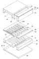
図1は、本発明の実施形態1に係るインクジェット式記録ヘッドを示す分解斜視図であり、図2は、図1の平面図及び断面図である。図示するように、流路形成基板10は、本実施形態では面方位(110)のシリコン単結晶基板からなり、その一方の面には予め熱酸化により形成した二酸化シリコンからなる、厚さ0.5〜2μmの弾性膜50が形成されている。流路形成基板10には、その他方面側から異方性エッチングすることにより形成され、隔壁11によって区画された複数の圧力発生室12がその幅方向に並設されている。また、流路形成基板10の圧力発生室12の長手方向外側の領域には連通部13が形成され、連通部13と各圧力発生室12とが、各圧力発生室12毎に設けられたインク供給路14を介して連通されている。なお、連通部13は、後述する保護基板のリザーバ部と連通して各圧力発生室12の共通のインク室となるリザーバの一部を構成する。インク供給路14は、圧力発生室12よりも狭い幅で形成されており、連通部13から圧力発生室12に流入するインクの流路抵抗を一定に保持している。Hereinafter, the present invention will be described in detail based on embodiments.
(Embodiment 1)
FIG. 1 is an exploded perspective view showing an ink jet recording head according to Embodiment 1 of the present invention, and FIG. 2 is a plan view and a cross-sectional view of FIG. As shown in the drawing, the flow
また、流路形成基板10の開口面側には、各圧力発生室12のインク供給路14とは反対側の端部近傍に連通するノズル開口21が穿設されたノズルプレート20が、後述するマスク膜を介して接着剤や熱溶着フィルム等によって固着されている。なお、ノズルプレート20は、厚さが例えば、0.01〜1mmで、線膨張係数が300℃以下で、例えば2.5〜4.5[×10-6/℃]であるガラスセラミックス、シリコン単結晶基板又はステンレス鋼などからなる。Further, a
一方、このような流路形成基板10の開口面側とは反対側には、上述したように、厚さが例えば約1.0μmの二酸化シリコン(SiO2)からなる弾性膜50が形成され、この弾性膜50上には、厚さが例えば、約0.4μmの酸化ジルコニウム(ZrO2)からなる絶縁体膜55が形成されている。また、この絶縁体膜55上には、厚さが例えば、約0.1〜0.2μmの下電極膜60と、厚さが例えば、約1.0μmの圧電体層70と、厚さが例えば、約0.05μmの上電極膜80とが、後述するプロセスで積層形成されて、圧電素子300を構成している。ここで、圧電素子300は、下電極膜60、圧電体層70及び上電極膜80を含む部分をいう。一般的には、圧電素子300の何れか一方の電極を共通電極とし、他方の電極及び圧電体層70を各圧力発生室12毎にパターニングして構成する。そして、ここではパターニングされた何れか一方の電極及び圧電体層70から構成され、両電極への電圧の印加により圧電歪みが生じる部分を圧電体能動部という。本実施形態では、下電極膜60を圧電素子300の共通電極とし、上電極膜80を圧電素子300の個別電極としているが、駆動回路や配線の都合でこれを逆にしても支障はない。何れの場合においても、各圧力発生室毎に圧電体能動部が形成されていることになる。また、ここでは、圧電素子300と当該圧電素子300の駆動により変位が生じる振動板とを合わせて圧電アクチュエータと称する。なお、上述した例では、弾性膜50、絶縁体膜55及び下電極膜60が振動板としての役割を果たす。On the other hand, an
また、このような各圧電素子300の上電極膜80には、リード電極90がそれぞれ接続され、このリード電極90を介して各圧電素子300に選択的に電圧が印加されるようになっている。 Further, a
ここで、本発明では、圧電素子300を構成する圧電体層70の下地となる振動板の最表層を構成する絶縁体膜55の表面粗さ(算術平均粗さRa)が1〜3nmの範囲内であり、好ましくは1.5nm以上であり、特に2nmより大きくなっていることが望ましい。なお、このような絶縁体膜55上に形成される下電極膜60の表面粗さRaも1〜3nm以下となっている。詳しくは後述するが、このように絶縁体膜55の表面粗さRaを比較的大きくすることで、この絶縁体膜55上に形成される圧電体層70の特性を向上させることができる。 Here, in the present invention, the surface roughness (arithmetic average roughness Ra) of the
また、流路形成基板10上の圧電素子300側の面には、圧電素子300に対向する領域に圧電素子保持部31を有する保護基板30が接着剤を介して接合されている。圧電素子300は、この圧電素子保持部31内に形成されているため、外部環境の影響を殆ど受けない状態で保護されている。さらに、保護基板30には、流路形成基板10の連通部13に対応する領域にリザーバ部32が設けられている。このリザーバ部32は、本実施形態では、保護基板30を厚さ方向に貫通して圧力発生室12の並設方向に沿って設けられており、上述したように流路形成基板10の連通部13と連通されて各圧力発生室12の共通のインク室となるリザーバ100を構成している。 Further, the
また、保護基板30の圧電素子保持部31とリザーバ部32との間の領域には、保護基板30を厚さ方向に貫通する貫通孔33が設けられ、この貫通孔33内に下電極膜60の一部及びリード電極90の先端部が露出され、これら下電極膜60及びリード電極90には、図示しないが、一端が駆動ICに接続された接続配線の他端が接続される。 In addition, a
なお、保護基板30の材料としては、例えば、ガラス、セラミックス材料、金属、樹脂等が挙げられるが、流路形成基板10の熱膨張率と略同一の材料で形成されていることがより好ましく、本実施形態では、流路形成基板10と同一材料のシリコン単結晶基板を用いて形成した。 In addition, examples of the material of the
また、保護基板30上には、封止膜41及び固定板42とからなるコンプライアンス基板40が接合されている。封止膜41は、剛性が低く可撓性を有する材料(例えば、厚さが6μmのポリフェニレンサルファイド(PPS)フィルム)からなり、この封止膜41によってリザーバ部32の一方面が封止されている。また、固定板42は、金属等の硬質の材料(例えば、厚さが30μmのステンレス鋼(SUS)等)で形成される。この固定板42のリザーバ100に対向する領域は、厚さ方向に完全に除去された開口部43となっているため、リザーバ100の一方面は可撓性を有する封止膜41のみで封止されている。 A
このような本実施形態のインクジェット式記録ヘッドでは、図示しない外部インク供給手段からインクを取り込み、リザーバ100からノズル開口21に至るまで内部をインクで満たした後、図示しない駆動ICからの記録信号に従い、圧力発生室12に対応するそれぞれの下電極膜60と上電極膜80との間に電圧を印加し、弾性膜50、絶縁体膜55、下電極膜60及び圧電体層70をたわみ変形させることにより、各圧力発生室12内の圧力が高まりノズル開口21からインクが吐出する。 In such an ink jet recording head of this embodiment, ink is taken in from an external ink supply means (not shown), filled with ink from the
ここで、このようなインクジェット式記録ヘッドの製造方法について、図3〜図6を参照して説明する。なお、図3〜図6は、圧力発生室12の長手方向の断面図である。まず、図3(a)に示すように、シリコンウェハである流路形成基板用ウェハ110を約1100℃の拡散炉で熱酸化し、その表面に弾性膜50を構成する二酸化シリコン膜51を形成する。なお、本実施形態では、流路形成基板10として、膜厚が約625μmと比較的厚く剛性の高いシリコンウェハを用いている。 Here, a method of manufacturing such an ink jet recording head will be described with reference to FIGS. 3 to 6 are cross-sectional views of the
次いで、図3(b)に示すように、弾性膜50(二酸化シリコン膜51)上に、酸化ジルコニウムからなる絶縁体膜55を形成する。具体的には、弾性膜50(二酸化シリコン膜51)上に、DCスパッタ法又はRFスパッタ法等によりジルコニウム(Zr)層を形成する。このとき、ジルコニウム層の表面粗さ(算術平均粗さRa)が1〜3nmとなるように制御し、好ましくは1.5nm以上、さらに好ましくは2.0nmより大きくなるように制御する。 Next, as shown in FIG. 3B, an
さらに、ジルコニウム層は、その表面の(002)面配向度が80%以上となっていることが好ましい。なお、ここで言う「配向度」とは、X線回折広角法によってジルコニウム層を測定した際に生じる回折強度の比率をいう。具体的には、ジルコニウム層をX線回折広角法により測定すると、(100)面、(002)面及び(101)面に相当する回折強度のピークが発生する。そして、「(002)面配向度」とは、これら各面に相当するピーク強度の和に対する(002)面に相当するピーク強度の比率を意味する。 Furthermore, it is preferable that the (002) plane orientation degree of the surface of the zirconium layer is 80% or more. The “orientation degree” here refers to the ratio of the diffraction intensity generated when the zirconium layer is measured by the X-ray diffraction wide angle method. Specifically, when the zirconium layer is measured by the X-ray diffraction wide angle method, peaks of diffraction intensity corresponding to the (100) plane, the (002) plane, and the (101) plane are generated. The “(002) plane orientation degree” means the ratio of the peak intensity corresponding to the (002) plane to the sum of the peak intensity corresponding to each plane.
そして、このようにジルコニウム層の表面粗さRaを1〜3nmの範囲内とするためには、ジルコニウム層を形成する際のスパッタ出力を500W以下とすることが好ましい。また、スパッタ温度は常温(約23〜25℃)とすることが好ましい。さらに、スパッタ圧力は0.5Pa以上とするのが好ましい。また、ターゲット間隔(ターゲットと基板との間の距離)を100mm以下とするのが好ましい。このように成膜条件を適宜選択してジルコニウム層を形成することにより、ジルコニウム層の表面粗さRaを1〜3nmの範囲内に制御することができ、また同時に(002)面配向度を80%以上とすることができる。 And in order to make surface roughness Ra of a zirconium layer into the range of 1-3 nm in this way, it is preferable that the sputter | spatter output at the time of forming a zirconium layer shall be 500 W or less. The sputtering temperature is preferably room temperature (about 23 to 25 ° C.). Furthermore, the sputtering pressure is preferably 0.5 Pa or more. Further, the target interval (distance between the target and the substrate) is preferably set to 100 mm or less. Thus, by appropriately selecting the film forming conditions and forming the zirconium layer, the surface roughness Ra of the zirconium layer can be controlled within the range of 1 to 3 nm, and at the same time the (002) plane orientation degree is 80. % Or more.
このようにジルコニウム層を形成した後は、このジルコニウム層を熱酸化して酸化ジルコニウムからなる絶縁体膜55を形成する。このときの加熱温度は、900℃以下、好ましくは700〜900℃の範囲内とするのがよい。このように熱酸化時の加熱温度を調整することで、絶縁体膜55の表面粗さRaが1〜3nmの範囲内となるように形成する。例えば、本実施形態では、約700〜900℃に加熱された酸素雰囲気下の拡散炉内に、300mm/min以上、好ましくは500mm/min以上のスピードで流路形成基板用ウェハ110を挿入してジルコニウム層を約15〜60分間熱酸化させるようにした。 After the zirconium layer is thus formed, the zirconium layer is thermally oxidized to form an
これにより、結晶状態が良好な絶縁体膜55が得られ、その絶縁体膜55の表面粗さRaが1〜3nmの範囲内となる。すなわち、絶縁体膜55を構成する酸化ジルコニウムの結晶が略均一に成長して下面から上面まで連続的な柱状結晶となることで、表面粗さRaが1〜3nmの範囲内と比較的粗くなる。 Thereby, the
次いで、図3(c)に示すように、例えば、少なくとも白金とイリジウムとからなる下電極膜60を絶縁体膜55の全面にスパッタ法等により形成後、下電極膜60を所定形状にパターニングする。なお、この下電極膜60の表面粗さRaは、絶縁体膜55の表面粗さRaに依存するため、絶縁体膜55の表面粗さRaが1〜3nmの範囲内であると、下電極膜60の表面粗さRaも1〜3nmの範囲内となる。 Next, as shown in FIG. 3C, for example, a
次に、図3(d)に示すように、下電極膜60及び絶縁体膜55上に、チタン(Ti)をスパッタ法、例えば、DCスパッタ法で2回以上、本実施形態では2回塗布することにより所定の厚さで連続する種チタン層65を形成する。この種チタン層65の膜厚は、1nm〜8nmの範囲内となるように形成するのが好ましい。種チタン層65をこのような厚さで形成することにより、後述する工程で形成される圧電体層70の結晶性を向上させることができるからである。 Next, as shown in FIG. 3D, on the
ここで、種チタン層65を形成する際のスパッタ条件は特に限定されないが、スパッタ圧力は、0.4〜4.0Paの範囲内であるのが好ましい。また、スパッタ出力は50〜100Wとするのが好ましく、スパッタ温度は常温(約23〜25℃)〜200℃の範囲内とするのが好ましい。さらに、パワー密度は1〜4kW/m2程度とすることが好ましい。また、上述したように、ここではチタンを2回塗布することで、次工程で形成する圧電体層70の結晶の核となる種チタンを多数形成することができる。Here, the sputtering conditions for forming the
次に、このように形成した種チタン層65上に、例えば、チタン酸ジルコン酸鉛(PZT)からなる圧電体層70を形成する。本実施形態では、金属有機物を触媒に溶解・分散したいわゆるゾルを塗布乾燥してゲル化し、さらに高温で焼成することで金属酸化物からなる圧電体層70を得る、いわゆるゾル−ゲル法を用いてPZTからなる圧電体層70を形成した。 Next, a
圧電体層70の形成手順としては、まず、図4(a)に示すように、種チタン層65上にPZT前駆体膜である圧電体前駆体膜71を成膜する。すなわち、流路形成基板用ウェハ110上に金属有機化合物を含むゾル(溶液)を塗布する。次いで、圧電体前駆体膜71を、所定温度に加熱して一定時間乾燥させ、ゾルの溶媒を蒸発させることで圧電体前駆体膜71を乾燥させる。さらに、大気雰囲気下において一定の温度で一定時間、圧電体前駆体膜71を脱脂する。なお、ここでいう脱脂とは、圧電体前駆体膜71に含まれる有機成分を、例えば、NO2、CO2、H2O等として離脱させることである。As a procedure for forming the
そして、このような塗布・乾燥・脱脂の工程を、所定回数、例えば、本実施形態では、2回繰り返すことで、図4(b)に示すように、圧電体前駆体膜71を所定厚に形成し、この圧電体前駆体膜71を拡散炉で加熱処理することによって結晶化させて圧電体膜72を形成する。すなわち、圧電体前駆体膜71を焼成することで種チタン層65を核として結晶が成長して圧電体膜72が形成される。例えば、本実施形態では、約700℃で30分間加熱を行って圧電体前駆体膜71を焼成して圧電体膜72を形成した。なお、このように形成した圧電体膜72の結晶は(100)面に優先配向する。 Then, by repeating such coating, drying, and degreasing processes a predetermined number of times, for example, twice in the present embodiment, the
さらに、上述した塗布・乾燥・脱脂・焼成の工程を、複数回繰り返すことにより、図4(c)に示すように、複数層、本実施形態では、5層の圧電体膜72からなる所定厚さの圧電体層70を形成する。例えば、ゾルの塗布1回あたりの膜厚が0.1μm程度の場合には、圧電体層70全体の膜厚は約1μmとなる。 Further, by repeating the above-described coating, drying, degreasing, and firing steps a plurality of times, as shown in FIG. 4C, a predetermined thickness composed of a plurality of layers, in this embodiment, five layers of
以上のような工程で圧電体層70を形成することにより、圧電体層70の特性を向上させることができ且つ特性を安定させることができる。すなわち、圧電体層70の結晶性、例えば、配向度、強度、粒径等は、その下地の影響を受けやすく、その下地となる下電極膜60及び絶縁体膜55の表面粗さRaが比較的粗い程、結晶性は向上する傾向にあるが、あまり粗すぎると、結晶性が悪くなってしまう。本発明では、圧電体層70の下地となる振動板を構成する最表層である絶縁体膜55の表面粗さRaを1〜3nmの範囲内に制御することで、下電極膜60の表面粗さRaを1〜3nmの範囲内に制御すると共にこの下電極膜60上に形成される圧電体層70の結晶性を向上させている。これにより、電気的及び機械的特性に優れた圧電体層70を形成することができる。また、同一ウェハ内での圧電体層70の特性のばらつきも極めて小さく抑えることができる。 By forming the
さらに、圧電体層70の結晶性をコントロールしやすくなり、所望の特性の圧電体層70を比較的容易に製造することができ、量産性も大幅に向上する。すなわち、本発明では、絶縁体膜55の表面粗さRaを1〜3nmの範囲内となるように制御することで、この上に種チタン層65を形成する際のスパッタ条件を厳密に制御しなくても、絶縁体層の表面粗さRaを所定の範囲以外とした場合と比べて、この上に形成される圧電体層70の特性を比較的容易に向上させることができ且つ圧電体層70の特性を比較的容易に安定させることができる。これにより、歩留まりを向上することができる。 Furthermore, the crystallinity of the
なお、圧電体層70の材料としては、例えば、チタン酸ジルコン酸鉛(PZT)等の強誘電性圧電性材料に、ニオブ、ニッケル、マグネシウム、ビスマス又はイットリウム等の金属を添加したリラクサ強誘電体等を用いてもよい。その組成は、圧電素子の特性、用途等を考慮して適宜選択すればよいが、例えば、PbTiO3(PT)、PbZrO3(PZ)、Pb(ZrxTi1−x)O3(PZT)、Pb(Mg1/3Nb2/3)O3−PbTiO3(PMN−PT)、Pb(Zn1/3Nb2/3)O3−PbTiO3(PZN−PT)、Pb(Ni1/3Nb2/3)O3−PbTiO3(PNN−PT)、Pb(In1/2Nb1/2)O3−PbTiO3(PIN−PT)、Pb(Sc1/3Ta2/3)O3−PbTiO3(PST−PT)、Pb(Sc1/3Nb2/3)O3−PbTiO3(PSN−PT)、BiScO3−PbTiO3(BS−PT)、BiYbO3−PbTiO3(BY−PT)等が挙げられる。また、圧電体層70の製造方法は、ゾル−ゲル法に限定されず、例えば、MOD(Metal-Organic Decomposition)法等を用いてもよい。As a material of the
また、このように圧電体層70を形成した後は、図5(a)に示すように、例えば、イリジウムからなる上電極膜80を流路形成基板用ウェハ110の全面に形成する。次いで、図5(b)に示すように、圧電体層70及び上電極膜80を、各圧力発生室12に対向する領域にパターニングして圧電素子300を形成する。次に、リード電極90を形成する。具体的には、図5(c)に示すように、流路形成基板用ウェハ110の全面に亘って、例えば、金(Au)等からなる金属層91を形成する。その後、例えば、レジスト等からなるマスクパターン(図示なし)を介して金属層91を圧電素子300毎にパターニングすることでリード電極90が形成される。 After the
次に、図5(d)に示すように、流路形成基板用ウェハ110の圧電素子300側に、シリコンウェハであり複数の保護基板30となる保護基板用ウェハ130を接合する。なお、この保護基板用ウェハ130は、例えば、400μm程度の厚さを有するため、保護基板用ウェハ130を接合することによって流路形成基板用ウェハ110の剛性は著しく向上することになる。 Next, as shown in FIG. 5D, a
次いで、図6(a)に示すように、流路形成基板用ウェハ110をある程度の厚さとなるまで研磨した後、さらにフッ硝酸によってウェットエッチングすることにより流路形成基板用ウェハ110を所定の厚みにする。例えば、本実施形態では、約70μm厚になるように流路形成基板用ウェハ110をエッチング加工した。次いで、図6(b)に示すように、流路形成基板用ウェハ110上に、例えば、窒化シリコン(SiN)からなるマスク膜52を新たに形成し、所定形状にパターニングする。そして、このマスク膜52を介して流路形成基板用ウェハ110を異方性エッチングすることにより、図6(c)に示すように、流路形成基板用ウェハ110に圧力発生室12、連通部13及びインク供給路14等を形成する。 Next, as shown in FIG. 6A, after the flow path forming
なお、その後は、流路形成基板用ウェハ110及び保護基板用ウェハ130の外周縁部の不要部分を、例えば、ダイシング等により切断することによって除去する。そして、流路形成基板用ウェハ110の保護基板用ウェハ130とは反対側の面にノズル開口21が穿設されたノズルプレート20を接合すると共に、保護基板用ウェハ130にコンプライアンス基板40を接合し、流路形成基板用ウェハ110等を図1に示すような一つのチップサイズの流路形成基板10等に分割することによって、本実施形態のインクジェット式記録ヘッドとする。 After that, unnecessary portions of the outer peripheral edge portions of the flow path forming
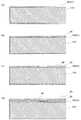
ここで、スパッタ圧力を約0.5Pa、スパッタ出力を500W、ターゲット間隔(ターゲットと基板との間の距離)を約65mmとして、弾性膜上に表面粗さRaが約2.2nmのジルコニウム層を形成した後に、約700〜900℃で約15〜60分間熱酸化し、絶縁体膜を形成した以外は、上述した製造方法により作製したものを実施例1のインクジェット式記録ヘッドとした。この実施例1のヘッドの圧電体層(PZT層)の表面粗さRaは約2.1nmであった。図7(a)には、実施例1の圧電体層の表面のSEM(走査電子顕微鏡)写真を示す。 Here, a zirconium layer having a surface roughness Ra of about 2.2 nm is formed on the elastic film with a sputtering pressure of about 0.5 Pa, a sputtering output of 500 W, a target interval (distance between the target and the substrate) of about 65 mm. After the formation, the ink jet recording head of Example 1 was prepared by the above-described manufacturing method except that the insulator film was formed by thermal oxidation at about 700 to 900 ° C. for about 15 to 60 minutes. The surface roughness Ra of the piezoelectric layer (PZT layer) of the head of Example 1 was about 2.1 nm. FIG. 7A shows a SEM (scanning electron microscope) photograph of the surface of the piezoelectric layer of Example 1. FIG.
比較のため、ジルコニウム層を形成する際のスパッタ条件として、スパッタ圧力を0.3Pa、スパッタ出力を1000W、ターゲット間隔を170mmとした以外は、実施例1と同様にして作製したものを比較例1のインクジェット式記録ヘッドとした。この比較例1のヘッドの圧電体層(PZT)の表面粗さRaは約0.8nmであった。図7(b)には、比較例1の圧電体層の表面のSEM写真を示す。 For comparison, Comparative Example 1 was prepared in the same manner as in Example 1 except that the sputtering conditions for forming the zirconium layer were sputtering pressure of 0.3 Pa, sputtering output of 1000 W, and target spacing of 170 mm. Inkjet recording head. The surface roughness Ra of the piezoelectric layer (PZT) of the head of Comparative Example 1 was about 0.8 nm. FIG. 7B shows an SEM photograph of the surface of the piezoelectric layer of Comparative Example 1.
図7(a)及び図7(b)に示すように、実施例1の圧電体層は、比較例1の圧電体層よりも緻密な層となっているのが確認できる。そして、上記実施例1及び比較例1のヘッドについて、圧電素子(圧電体層)の特性を比較したところ、比較例1のヘッドよりも実施例1のヘッドの方が圧電体層の特性が高いことが分った。 As shown in FIGS. 7A and 7B, it can be confirmed that the piezoelectric layer of Example 1 is a denser layer than the piezoelectric layer of Comparative Example 1. When the characteristics of the piezoelectric element (piezoelectric layer) were compared for the heads of Example 1 and Comparative Example 1, the head of Example 1 had higher characteristics of the piezoelectric layer than the head of Comparative Example 1. I found out.
(他の実施形態)
以上、本発明の一実施形態について説明したが、本発明は、上述した実施形態に限定されるものではない。例えば、上述した実施形態においては、液体噴射装置に用いるヘッドの一例としてインクジェット式記録ヘッドを例示したが、本発明は、広く液体噴射ヘッドの全般を対象としたものであり、インク以外の液体を噴射するものにも勿論適用することができる。その他の液体噴射ヘッドとしては、例えば、プリンタ等の画像記録装置に用いられる各種の記録ヘッド、液晶ディスプレー等のカラーフィルタの製造に用いられる色材噴射ヘッド、有機ELディスプレー、FED(面発光ディスプレー)等の電極形成に用いられる電極材料噴射ヘッド、バイオchip製造に用いられる生体有機物噴射ヘッド等が挙げられる。また、本発明は、このような液体噴射ヘッド(インクジェット式記録ヘッド)に液体吐出手段として搭載されるアクチュエータ装置だけでなく、あらゆる装置に搭載されるアクチュエータ装置に適用することができる。例えば、アクチュエータ装置は、上述したヘッドの他に、センサー等にも適用することができる。(Other embodiments)
Although one embodiment of the present invention has been described above, the present invention is not limited to the above-described embodiment. For example, in the above-described embodiment, an ink jet recording head is exemplified as an example of a head used in the liquid ejecting apparatus. However, the present invention is widely intended for the entire liquid ejecting head, and a liquid other than ink is used. Of course, the present invention can also be applied to a jet. Other liquid ejecting heads include, for example, various recording heads used in image recording apparatuses such as printers, color material ejecting heads used in the manufacture of color filters such as liquid crystal displays, organic EL displays, and FEDs (surface emitting displays). Examples thereof include an electrode material ejection head used for electrode formation, a bioorganic matter ejection head used for biochip production, and the like. The present invention can be applied not only to an actuator device mounted as liquid ejecting means on such a liquid jet head (inkjet recording head) but also to an actuator device mounted on any device. For example, the actuator device can be applied to a sensor or the like in addition to the head described above.
10 流路形成基板、 12 圧力発生室、 20 ノズルプレート、 21 ノズル開口、 30 保護基板、 40 コンプライアンス基板、 50 弾性膜、 55 絶縁体膜、 60 下電極膜、 65 種チタン層、 70 圧電体層、 80 上電極膜、 300 圧電素子
DESCRIPTION OF
Claims (7)
Translated fromJapanese前記絶縁体膜上に、下電極、圧電体層および上電極を含む圧電素子を形成する工程と、を備えた圧電アクチュエータの製造方法であって、
前記絶縁体膜の表面粗さRaが、2nmより大きく3nm以下の範囲内であることを特徴とするアクチュエータ装置の製造方法。Forming an insulator film made of zirconium oxide;
Forming a piezoelectric element including a lower electrode, a piezoelectric layer and an upper electrode on the insulator film, and a method of manufacturing a piezoelectric actuator comprising:
A method of manufacturing an actuator device, wherein the surface roughness Ra of the insulator film is in a rangegreater than 2 nm and less than or equal to3 nm .
Priority Applications (3)
| Application Number | Priority Date | Filing Date | Title |
|---|---|---|---|
| JP2004376892AJP4737375B2 (en) | 2004-03-11 | 2004-12-27 | Method for manufacturing actuator device, method for manufacturing liquid jet head, and method for manufacturing liquid jet device |
| US11/076,028US7320163B2 (en) | 2004-03-11 | 2005-03-10 | Method of manufacturing an actuator device |
| CNB2005100538439ACN1323842C (en) | 2004-03-11 | 2005-03-11 | Method of manufacturing actuator device, and liquid jet device |
Applications Claiming Priority (3)
| Application Number | Priority Date | Filing Date | Title |
|---|---|---|---|
| JP2004069660 | 2004-03-11 | ||
| JP2004069660 | 2004-03-11 | ||
| JP2004376892AJP4737375B2 (en) | 2004-03-11 | 2004-12-27 | Method for manufacturing actuator device, method for manufacturing liquid jet head, and method for manufacturing liquid jet device |
Publications (2)
| Publication Number | Publication Date |
|---|---|
| JP2005295786A JP2005295786A (en) | 2005-10-20 |
| JP4737375B2true JP4737375B2 (en) | 2011-07-27 |
Family
ID=34987990
Family Applications (1)
| Application Number | Title | Priority Date | Filing Date |
|---|---|---|---|
| JP2004376892AExpired - Fee RelatedJP4737375B2 (en) | 2004-03-11 | 2004-12-27 | Method for manufacturing actuator device, method for manufacturing liquid jet head, and method for manufacturing liquid jet device |
Country Status (3)
| Country | Link |
|---|---|
| US (1) | US7320163B2 (en) |
| JP (1) | JP4737375B2 (en) |
| CN (1) | CN1323842C (en) |
Families Citing this family (22)
| Publication number | Priority date | Publication date | Assignee | Title |
|---|---|---|---|---|
| US7578943B2 (en)* | 2005-05-23 | 2009-08-25 | Canon Kabushiki Kaisha | Liquid discharge head and producing method therefor |
| JP2007152912A (en)* | 2005-12-08 | 2007-06-21 | Seiko Epson Corp | Piezoelectric element manufacturing method, piezoelectric element, and liquid jet head |
| JP2007152913A (en)* | 2005-12-08 | 2007-06-21 | Seiko Epson Corp | Method for manufacturing piezoelectric element and method for manufacturing liquid jet head |
| JP5201304B2 (en)* | 2006-03-28 | 2013-06-05 | セイコーエプソン株式会社 | Method for manufacturing actuator device and method for manufacturing liquid jet head |
| US20070257580A1 (en)* | 2006-05-05 | 2007-11-08 | Fujifilm Dimatix, Inc. | Polishing Piezoelectric Material |
| JP4296441B2 (en) | 2006-10-11 | 2009-07-15 | セイコーエプソン株式会社 | Method for manufacturing actuator device |
| JP5083499B2 (en)* | 2006-11-13 | 2012-11-28 | セイコーエプソン株式会社 | Method for manufacturing actuator device and liquid jet head |
| JP5344120B2 (en) | 2007-07-05 | 2013-11-20 | セイコーエプソン株式会社 | Actuator device, manufacturing method thereof, and liquid jet head |
| JP2009038274A (en)* | 2007-08-03 | 2009-02-19 | Seiko Epson Corp | Piezoelectric element and manufacturing method thereof, actuator, and liquid jet head |
| JP5187489B2 (en)* | 2007-09-20 | 2013-04-24 | セイコーエプソン株式会社 | Method for manufacturing actuator device and method for manufacturing liquid jet head |
| JP5592104B2 (en)* | 2009-02-17 | 2014-09-17 | 富士フイルム株式会社 | Piezoelectric film, piezoelectric element including the same, and liquid ejection device |
| JP5506035B2 (en)* | 2010-02-23 | 2014-05-28 | 富士フイルム株式会社 | Actuator manufacturing method |
| WO2012020638A1 (en) | 2010-08-12 | 2012-02-16 | 株式会社村田製作所 | Method for manufacturing piezoelectric thin film element, piezoelectric thin film element, and member for piezoelectric thin film element |
| JP5462774B2 (en) | 2010-11-30 | 2014-04-02 | 東芝テック株式会社 | Inkjet head manufacturing method and inkjet head |
| US9761785B2 (en) | 2011-10-17 | 2017-09-12 | The United States Of America As Represented By The Secretary Of The Army | Stylo-epitaxial piezoelectric and ferroelectric devices and method of manufacturing |
| US8866367B2 (en) | 2011-10-17 | 2014-10-21 | The United States Of America As Represented By The Secretary Of The Army | Thermally oxidized seed layers for the production of {001} textured electrodes and PZT devices and method of making |
| JP2013225546A (en)* | 2012-04-20 | 2013-10-31 | Konica Minolta Inc | Piezo electric element and process of manufacturing the same |
| CN102700258A (en)* | 2012-06-05 | 2012-10-03 | 杭州威士德喷码技术有限公司 | Upper ink fountain of spray head of large character code spraying machine |
| JP6205703B2 (en) | 2012-10-24 | 2017-10-04 | セイコーエプソン株式会社 | Actuator, liquid ejecting head, and liquid ejecting apparatus |
| JP2014240152A (en)* | 2013-06-12 | 2014-12-25 | セイコーエプソン株式会社 | Piezoelectric unit, liquid jet head, liquid jet apparatus, and method of manufacturing piezoelectric unit |
| CN112470298B (en)* | 2018-07-30 | 2024-05-28 | 株式会社村田制作所 | MEMS device |
| JP7363067B2 (en) | 2019-03-19 | 2023-10-18 | 株式会社リコー | Piezoelectric thin film element, liquid ejection head, head module, liquid ejection unit, device for ejecting liquid, and method for manufacturing piezoelectric thin film element |
Family Cites Families (16)
| Publication number | Priority date | Publication date | Assignee | Title |
|---|---|---|---|---|
| JPH05177831A (en)* | 1991-12-27 | 1993-07-20 | Rohm Co Ltd | Ink jet printing head and electronic device equipped therewith |
| JP3890634B2 (en)* | 1995-09-19 | 2007-03-07 | セイコーエプソン株式会社 | Piezoelectric thin film element and ink jet recording head |
| US5900283A (en)* | 1996-11-12 | 1999-05-04 | General Electric Company | Method for providing a protective coating on a metal-based substrate and related articles |
| JP3627482B2 (en)* | 1997-12-08 | 2005-03-09 | 富士ゼロックス株式会社 | Manufacturing method of microstructure |
| JP2000332313A (en)* | 1999-05-21 | 2000-11-30 | Matsushita Electric Ind Co Ltd | Thin-film piezoelectric bimorph device and its application |
| JP2000349362A (en)* | 1999-06-02 | 2000-12-15 | Japan Fine Ceramics Center | Piezoelectric device and its manufacture |
| US6329305B1 (en)* | 2000-02-11 | 2001-12-11 | Agere Systems Guardian Corp. | Method for producing devices having piezoelectric films |
| US6342134B1 (en)* | 2000-02-11 | 2002-01-29 | Agere Systems Guardian Corp. | Method for producing piezoelectric films with rotating magnetron sputtering system |
| US6494567B2 (en)* | 2000-03-24 | 2002-12-17 | Seiko Epson Corporation | Piezoelectric element and manufacturing method and manufacturing device thereof |
| JP3567977B2 (en) | 2000-03-24 | 2004-09-22 | セイコーエプソン株式会社 | Piezoelectric element, ink jet recording head, printer, and method of manufacturing piezoelectric element |
| JP3796394B2 (en)* | 2000-06-21 | 2006-07-12 | キヤノン株式会社 | Method for manufacturing piezoelectric element and method for manufacturing liquid jet recording head |
| JP3833070B2 (en)* | 2001-02-09 | 2006-10-11 | キヤノン株式会社 | Liquid ejecting head and manufacturing method |
| JP2003046160A (en)* | 2001-04-26 | 2003-02-14 | Matsushita Electric Ind Co Ltd | Piezoelectric element, actuator and inkjet head |
| JP4212819B2 (en)* | 2002-03-08 | 2009-01-21 | 上田日本無線株式会社 | Method for manufacturing piezoelectric vibrator |
| JP3555682B2 (en)* | 2002-07-09 | 2004-08-18 | セイコーエプソン株式会社 | Liquid ejection head |
| JP3947443B2 (en)* | 2002-08-30 | 2007-07-18 | Tdk株式会社 | Electronic device substrate and electronic device |
- 2004
- 2004-12-27JPJP2004376892Apatent/JP4737375B2/ennot_activeExpired - Fee Related
- 2005
- 2005-03-10USUS11/076,028patent/US7320163B2/enactiveActive
- 2005-03-11CNCNB2005100538439Apatent/CN1323842C/ennot_activeExpired - Fee Related
Also Published As
| Publication number | Publication date |
|---|---|
| CN1323842C (en) | 2007-07-04 |
| JP2005295786A (en) | 2005-10-20 |
| CN1666870A (en) | 2005-09-14 |
| US20050210645A1 (en) | 2005-09-29 |
| US7320163B2 (en) | 2008-01-22 |
Similar Documents
| Publication | Publication Date | Title |
|---|---|---|
| JP4737375B2 (en) | Method for manufacturing actuator device, method for manufacturing liquid jet head, and method for manufacturing liquid jet device | |
| JP5019020B2 (en) | Dielectric film manufacturing method, piezoelectric element manufacturing method, and liquid jet head manufacturing method | |
| JP4296441B2 (en) | Method for manufacturing actuator device | |
| JP2008091877A (en) | Piezoelectric element, actuator device, liquid jet head, and liquid jet device | |
| JP5024518B2 (en) | Actuator device, liquid jet head, and image recording apparatus | |
| JP5013035B2 (en) | Dielectric film manufacturing method and liquid jet head manufacturing method | |
| JP2007073931A (en) | Manufacturing method of actuator device, actuator device, liquid jet head, and liquid jet device | |
| JP2006093312A (en) | Piezoelectric element, liquid ejecting head, liquid ejecting apparatus, and method of manufacturing piezoelectric element | |
| JP4877451B2 (en) | Piezoelectric element manufacturing method and liquid jet head | |
| JP5310969B2 (en) | LAMINATED FILM MANUFACTURING METHOD, ACTUATOR DEVICE MANUFACTURING METHOD, ACTUATOR DEVICE, LIQUID EJECTING HEAD, AND LIQUID EJECTING DEVICE | |
| KR100816169B1 (en) | Method for manufacturing actuator device and actuator device and liquid spray head and liquid ejection device | |
| JP5201304B2 (en) | Method for manufacturing actuator device and method for manufacturing liquid jet head | |
| JP2008205048A (en) | Method for manufacturing piezoelectric element and method for manufacturing liquid jet head | |
| JP2005260003A (en) | Method for manufacturing actuator device and liquid ejecting apparatus | |
| JP5099303B2 (en) | Liquid ejecting head and manufacturing method thereof | |
| JP2005209912A (en) | Piezoelectric element, liquid jet head, and method of manufacturing piezoelectric element | |
| JP2007173691A (en) | Piezoelectric element manufacturing method, actuator device, and liquid jet head | |
| JP5024564B2 (en) | Actuator device and liquid jet head | |
| JP2006019513A (en) | Method for manufacturing piezoelectric element and method for manufacturing liquid jet head | |
| JP2006021392A (en) | Actuator apparatus and its manufacturing method, and liquid jet apparatus | |
| JP2006161066A (en) | Sputtering target, manufacturing method thereof, sputtering apparatus, and liquid jet head | |
| JP2006144090A (en) | Sputtering method, sputtering apparatus, piezoelectric element manufacturing method, and liquid jet head | |
| JP2007173605A (en) | Method for manufacturing piezoelectric element and method for manufacturing liquid jet head | |
| JP2006019592A (en) | Dielectric film manufacturing method, piezoelectric element manufacturing method, and liquid jet head manufacturing method | |
| JP5083499B2 (en) | Method for manufacturing actuator device and liquid jet head |
Legal Events
| Date | Code | Title | Description |
|---|---|---|---|
| A621 | Written request for application examination | Free format text:JAPANESE INTERMEDIATE CODE: A621 Effective date:20070713 | |
| A977 | Report on retrieval | Free format text:JAPANESE INTERMEDIATE CODE: A971007 Effective date:20100331 | |
| A131 | Notification of reasons for refusal | Free format text:JAPANESE INTERMEDIATE CODE: A131 Effective date:20100407 | |
| A521 | Request for written amendment filed | Free format text:JAPANESE INTERMEDIATE CODE: A523 Effective date:20100607 | |
| A02 | Decision of refusal | Free format text:JAPANESE INTERMEDIATE CODE: A02 Effective date:20100929 | |
| A521 | Request for written amendment filed | Free format text:JAPANESE INTERMEDIATE CODE: A523 Effective date:20101228 | |
| A911 | Transfer to examiner for re-examination before appeal (zenchi) | Free format text:JAPANESE INTERMEDIATE CODE: A911 Effective date:20110217 | |
| TRDD | Decision of grant or rejection written | ||
| A01 | Written decision to grant a patent or to grant a registration (utility model) | Free format text:JAPANESE INTERMEDIATE CODE: A01 Effective date:20110406 | |
| A61 | First payment of annual fees (during grant procedure) | Free format text:JAPANESE INTERMEDIATE CODE: A61 Effective date:20110419 | |
| R150 | Certificate of patent or registration of utility model | Ref document number:4737375 Country of ref document:JP Free format text:JAPANESE INTERMEDIATE CODE: R150 Free format text:JAPANESE INTERMEDIATE CODE: R150 | |
| FPAY | Renewal fee payment (event date is renewal date of database) | Free format text:PAYMENT UNTIL: 20140513 Year of fee payment:3 | |
| S531 | Written request for registration of change of domicile | Free format text:JAPANESE INTERMEDIATE CODE: R313531 | |
| R350 | Written notification of registration of transfer | Free format text:JAPANESE INTERMEDIATE CODE: R350 | |
| LAPS | Cancellation because of no payment of annual fees |