JP4733877B2 - Semiconductor device - Google Patents
Semiconductor deviceDownload PDFInfo
- Publication number
- JP4733877B2 JP4733877B2JP2001246654AJP2001246654AJP4733877B2JP 4733877 B2JP4733877 B2JP 4733877B2JP 2001246654 AJP2001246654 AJP 2001246654AJP 2001246654 AJP2001246654 AJP 2001246654AJP 4733877 B2JP4733877 B2JP 4733877B2
- Authority
- JP
- Japan
- Prior art keywords
- bus
- clock control
- clock
- signal
- module
- Prior art date
- Legal status (The legal status is an assumption and is not a legal conclusion. Google has not performed a legal analysis and makes no representation as to the accuracy of the status listed.)
- Expired - Fee Related
Links
Images


Classifications
- G—PHYSICS
- G06—COMPUTING OR CALCULATING; COUNTING
- G06F—ELECTRIC DIGITAL DATA PROCESSING
- G06F1/00—Details not covered by groups G06F3/00 - G06F13/00 and G06F21/00
- G06F1/26—Power supply means, e.g. regulation thereof
- G06F1/32—Means for saving power
- G06F1/3203—Power management, i.e. event-based initiation of a power-saving mode
- G06F1/3206—Monitoring of events, devices or parameters that trigger a change in power modality
- G06F1/3228—Monitoring task completion, e.g. by use of idle timers, stop commands or wait commands
- G—PHYSICS
- G06—COMPUTING OR CALCULATING; COUNTING
- G06F—ELECTRIC DIGITAL DATA PROCESSING
- G06F1/00—Details not covered by groups G06F3/00 - G06F13/00 and G06F21/00
- G06F1/26—Power supply means, e.g. regulation thereof
- G06F1/32—Means for saving power
- G06F1/3203—Power management, i.e. event-based initiation of a power-saving mode
- G06F1/3234—Power saving characterised by the action undertaken
- G06F1/324—Power saving characterised by the action undertaken by lowering clock frequency
- Y—GENERAL TAGGING OF NEW TECHNOLOGICAL DEVELOPMENTS; GENERAL TAGGING OF CROSS-SECTIONAL TECHNOLOGIES SPANNING OVER SEVERAL SECTIONS OF THE IPC; TECHNICAL SUBJECTS COVERED BY FORMER USPC CROSS-REFERENCE ART COLLECTIONS [XRACs] AND DIGESTS
- Y02—TECHNOLOGIES OR APPLICATIONS FOR MITIGATION OR ADAPTATION AGAINST CLIMATE CHANGE
- Y02D—CLIMATE CHANGE MITIGATION TECHNOLOGIES IN INFORMATION AND COMMUNICATION TECHNOLOGIES [ICT], I.E. INFORMATION AND COMMUNICATION TECHNOLOGIES AIMING AT THE REDUCTION OF THEIR OWN ENERGY USE
- Y02D10/00—Energy efficient computing, e.g. low power processors, power management or thermal management
Landscapes
- Engineering & Computer Science (AREA)
- Theoretical Computer Science (AREA)
- Physics & Mathematics (AREA)
- General Engineering & Computer Science (AREA)
- General Physics & Mathematics (AREA)
- Information Transfer Systems (AREA)
- Executing Machine-Instructions (AREA)
- Power Sources (AREA)
- Bus Control (AREA)
- Microcomputers (AREA)
- Tests Of Electronic Circuits (AREA)
Description
Translated fromJapanese【0001】
【発明の属する技術分野】
本発明は、一般にクロック信号に同期して動作する半導体装置に関し、詳しくはクロック信号を制御することにより消費電力を削減可能な半導体装置に関する。
【従来の技術】
プロセッサ等の半導体装置においては、消費電力を削減するために、高速処理を必要としない期間のクロック周波数を低く抑える或いは停止させる制御が行われる。即ち、クロックの動作周波数を必要に応じて段階的に切りかえたり(以下「クロックギア」と呼ぶ)、或いは動作させる必要の無いモジュールブロックへのクロックを停止させる(以下「パワーダウンモード」と呼ぶ)制御が行われる。
クロックギアは、一般に、プロセッサ内の一番早いクロックに対応したマスク用の同期信号を供給し、ゲーテッドクロックバッファでクロック出力のパルス数を減らすことにより実現する。或いは分周回路でクロック信号を分周することにより実現する。またパワーダウンモードは、プロセッサ内の特定の一部或いは全部のモジュールに対して、動作の必要がない期間、それらモジュールへのクロック信号の供給をマスクすることにより実現する。これらのクロック制御は、チップの端子設定及びプログラムによるソフトウェア的な制御に基づいて、プロセッサ内のクロック制御部により実行するのが一般的である。
従来、プロセッサ内部のオンチップバスやバスブリッジを介する内部周辺バス等がある場合において、上記のようなクロックギア切り替え或いはパワーダウンモードへの遷移を行う際には、ソフトウェアによって一定の手順を実行する必要がある。即ち、クロックギアの切り替え或いはパワーダウンモードへの遷移をするためには、その準備として、バス転送等の特定のプロトコル(動作仕様)に沿った動作を、ソフトウェア的に完了させる必要がある。
【発明が解決しようとする課題】
例えば、このような手順を経ないで、バスを経由するデータ転送(特に命令フェッチ等)の最中にクロックギアの切り替え等をした場合、命令の取りこぼしによるプロセッサのハングアップを発生させる危険性がある。また例えば、バスブリッジを経由する内部周辺バスに接続されたモジュールへの突き放し制御のストア命令を実行する場合においては、オンチップバス上での転送が完了した後も内部周辺バスで引き続きライト動作が行われているので、ストア動作が実際に完了する時間まで待たずにクロックギアの切り替え等を行ってしまったのでは、ストアが正常に行われない危険性がある。また例えば、SDRAMコントローラをチップに搭載している場合においては、予めSDRAMをセルフリフレッシュモードへ遷移させずにSDRAMコントローラのクロックを停止したのでは、SDRAMのデータが破壊されてしまう。
【0002】
こうした問題を避けるために、クロックギア切り替えやパワーダウンモードへの遷移に際して所定の手順を実行するプログラムを、予め作成しておく必要がある。しかしその手順が完璧に実行されない場合には、予期せぬハングアップ等が発生する恐れがあった。
特に、複雑な転送プロトコルを持つオンチップバスや、バスブリッジ、チップ外部バス(SDRAM、SRAM、ROM、コンパニオンチップ等に接続するバス)等を持つプロセッサのクロック制御プログラムを作成する際には、種々の条件を考慮して制御する必要があるので、人為的なミスによるハングアップやデータ転送エラーの危険性を完全に排除することは容易でない。
【0003】
以上を鑑みて、本発明は、クロックギア切り替え時やパワーダウンモード遷移時等におけるハングアップの危険性を取り除くハードウェア機構を備えた半導体装置を提供することを目的とする。
【課題を解決するための手段】
本発明による半導体装置は、クロック信号を生成するクロック生成部と、クロック制御リクエスト信号をアサートする第1のモジュールと、該クロック制御リクエスト信号のアサート状態に応答して、現在実行中の処理が終了するとその後の処理を停止してクロック制御アクノリッジ信号をアサートする1つ又は複数の第2のモジュールと、オンチップバスと、該オンチップバスに接続される複数のモジュールと、該複数のモジュールのうちバスマスターであるモジュール間でバス権を調停するバスアービタと、チップ内部周辺バスと、該チップ内部周辺バスと該オンチップバスとを接続するバスブリッジとを含み、該1つ又は複数の第2のモジュールからの該クロック制御アクノリッジ信号が全てアサートされると該クロック生成部は該第2のモジュールに供給する該クロック信号を選択的に変化させ、該バスアービタは、該1つ又は複数の第2のモジュールのうちの1つであり、該クロック制御リクエスト信号のアサート状態に応答して、現在実行中の転送動作が終了すると該バスマスターであるモジュールに対する全てのバス権を不許可として該クロック制御アクノリッジ信号をアサートし、該バスブリッジは、該1つ又は複数の第2のモジュールのうちの1つであり、該クロック制御リクエスト信号のアサート状態に応答して、現在実行中のデータ転送処理が終了するとその後のデータ転送処理を停止して該クロック制御アクノリッジ信号をアサートする。
【0004】
以上のハードウェア制御によって、本発明においては、クロックギア切り替えやパワーダウンモード遷移等の処理を行う際に、クロック制御により動作に問題が生じる可能性があるモジュールを予め処理停止状態にし、誤動作の危険性が無い状態になってからクロック制御を実行することが可能となる。
【発明の実施の形態】
以下に、本発明の実施例を添付の図面を用いて詳細に説明する。
【0005】
図1は、本発明によるプロセッサの第1実施例の構成を示す図である。
【0006】
図1のプロセッサ10は、クロック制御部11、CPUコア部12、DSPコア部13、モジュール14、モジュール15、オンチップバス(OCB)と内蔵周辺バス(PB)のバスブリッジ16、DMAコントローラ17、SDRAMコントローラ18、外部バスコントローラ19、オンチップバスのバスアービタ20、オンチップバス(OCB)21、モジュール22乃至24、内部周辺バス(PB)25、プロセッサ10の外部に設けられ外部バスコントローラ19に接続されるSRAM26及び外部バスマスター・チップ27、外部バス28、プロセッサ10の外部に設けられSDRAMコントローラ18に接続されるSDRAM29を含む。ここで、CPUコア部12、DSPコア部13、モジュール14、モジュール15、DMAコントローラ17、SDRAMコントローラ18、外部バスコントローラ19は、オンチップバス21に接続されるオンチップバスモジュールであり、モジュール22乃至24は、内部周辺バス25に接続される周辺バスモジュールである。またSRAM26及び外部バスマスター・チップ27は、外部バス28に接続される外部バスモジュールである。
【0007】
クロック制御部11は、クロック生成部30と、クロック制御判定部31を含む。またモジュール22は、クロック制御レジスタ32を含む。
【0008】
以下に、本発明によるプロセッサ10の動作を説明する。
【0009】
プロセッサ10により特定のアプリケーションを動作させるためのソフトウェアを実行中に、プロセッサ10のクロック制御(ギア切り替えやパワーダウンモードへの遷移等)を行うとする。まずクロック制御を指示するために、内部周辺バス25に接続されるモジュール22のクロック制御レジスタ32に、クロック制御指示データのストア(ライト)命令をプログラムから発行する。具体的には、このストア命令に係るライトデータは、CPUコア部12から発行され、オンチップバス21の転送仕様に従ってバスブリッジ16へ転送される。更に、バスブリッジ16から、モジュール22へ当該ライトデータに関するライト要求が送出され、モジュール22内のクロック制御レジスタ32にライトデータが格納される。
【0010】
上記ライト動作に係るシーケンスの実行中において、CPUコア部12は、当該クロック制御指示データのストア命令を発行した後、パイプライン処理により順次後続する命令を実行する。
【0011】
クロック制御レジスタ32へ上記クロック制御指示データが格納されると、クロック制御レジスタ32から、クロック制御部11にクロック制御要求信号が発行される。このクロック制御要求信号は、クロック制御部11のクロック制御判定部31が受信する。クロック制御判定部31は、クロック制御要求信号がアサートされたことを認識すると、クロック制御対象の各モジュールに対してクロック制御リクエスト信号reqをアサートする。
【0012】
クロック制御リクエスト信号reqは、クロック制御完了通知信号DNがアサートされるまでの期間、アサート状態に維持される。
【0013】
クロック制御リクエスト信号reqを受け取った各モジュールは、その時点で実行中の処理が終了した時点で、その処理を一旦停止させ、クロック制御アクノリッジ信号ackx(x=0、1、2、・・・、6)をアサートする。ここで、クロック制御リクエスト信号reqを受け取り、クロック制御アクノリッジ信号をアサートするモジュールは、バスアービタ20、CPUコア部12、DSPコア部13、DMAコントローラ17、SDRAMコントローラ18、外部バスコントローラ19、及びバスブリッジ16である。バスアービタ20は、オンチップバス21に接続されるモジュール間でバス権を調停し、選択されたモジュールにバス権を与えることでバスに対するアクセスを許可する。バスブリッジ16は、オンチップバス21と内部周辺バス25との間のデータ転送を行う。
【0014】
例えば、バスアービタ20の場合、クロック制御リクエスト信号reqを受け取った後は、実行中のデータ転送のトランザクションが終了した時点で、全てのバスマスター(この例の場合、CPUコア部12、DSPコア部13、DMAコントローラ17、及び外部バスコントローラ19の各モジュール)へのバスグラント信号gntx(x=1、2、3、4)をネゲート状態にディアサートする。即ち、各マスターモジュールに対してバス権を否定することで、各マスターモジュールによるデータ転送を不許可にする。その後、バスアービタ20は、クロック制御アクノリッジ信号ack0をアサートする。
【0015】
クロック制御アクノリッジ信号ackxは、クロック制御リクエスト信号reqがネゲートされるまでの間、アサート状態に維持される。
【0016】
各クロック制御対象モジュールからのクロック制御アクノリッジ信号ackxの全てがアサートされると、クロック制御判定部31はこれを認識し、クロック生成部30に対して、クロック制御イネーブル信号ENをアサートする。この時、クロック制御対象となっている全てのモジュールは、動作を一時的に中断している。
【0017】
クロック生成部30は、クロック制御イネーブル信号ENがアサートされたのを確認すると、プログラムから要求されたクロック制御動作(クロックギアの切替やパワーダウンモードへの遷移等)を実行する。この際、クロック制御動作の詳細は、クロック制御レジスタ32に書き込まれたクロック制御指示データの内容によって指定される。クロック生成部30は、各モジュールに対してクロック信号を供給しており、プログラムからの要求に従って、各モジュールに供給するクロック信号を選択的に制御して、モジュール毎に動作周波数を変更したりクロック信号の供給を停止する。
【0018】
クロック生成部30は更に、クロック制御の処理が完了した時点で、クロック制御完了通知信号DNをアサートする。
【0019】
クロック制御判定部31は、クロック制御完了通知信号DNがアサートされたことを認識すると、クロック制御リクエスト信号reqをネゲートする。クロック制御リクエスト信号reqがネゲートされたことに応答して、各クロック制御対象モジュールは、クロック制御アクノリッジ信号ackxをネゲートする。クロック制御アクノリッジ信号ackxがネゲートされると、クロック制御イネーブル信号ENがネゲートされ、その後、クロック制御完了通知信号DNもネゲートされる。
【0020】
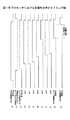
図2は、上記動作における各信号を示すタイミング図である。
【0021】
図2(a)に示されるようにクロック制御リクエスト信号reqがアサートされると、これに応答して、図2(b)に示されるようにバスグラント信号gntxがネゲート状態にされる。更に、各モジュールで現在実行中の動作が終了するタイミングで、図2(c)乃至(j)に示されるように、各モジュールからのクロック制御アクノリッジ信号ackxがHIGH(アサート状態)になる。
【0022】
全てのクロック制御アクノリッジ信号ackxがHIGHになると、図2(k)に示されるようにクロック制御イネーブル信号ENがHIGHになり、クロックギア切り替えやクロック停止等のクロック制御動作が実行される。このクロック制御動作が完了すると、図2(l)に示されるように、クロック制御完了通知信号DNがアサートされる。
【0023】
以上のハードウェア制御によって、本発明においては、クロックギア切り替えやパワーダウンモード遷移等の処理を行う際に、クロック制御により動作に問題が生じる可能性があるモジュールを予め処理停止状態にし、誤動作の危険性が無い状態になってからクロック制御を実行することが可能となる。
【0024】
図3は、クロック制御判定部31の構成例を示す図である。
【0025】
図3のクロック制御判定部31は、フリップフロップ41、フリップフロップ42−0乃至42−6、クロック制御デコーダ回路43、AND回路44、及びリクエスト信号生成回路45を含む。フリップフロップ41は、クロック制御レジスタ32から供給されるクロック制御要求信号をラッチする。ラッチされたクロック制御要求信号は、クロック制御デコーダ回路43に供給されてデコードされる。クロック制御要求信号は複数のビットからなる信号であり、クロック制御を要求すると共に、クロック制御がクロックギア切り替えとクロック停止の何れであるのか、どのモジュールに対するクロック制御であるのか等に関して、具体的な制御の詳細を指定する。クロック制御デコーダ回路43は、このクロック制御要求信号をデコードし、指定されたクロック制御動作を実行するための制御信号CTLを生成して、クロック生成部30に供給する。また更に、クロック制御デコーダ回路43は、クロック制御を示す信号clk_ctrをリクエスト信号生成回路45に供給する。リクエスト信号生成回路45は、単純なステートマシンであり、入力信号に応じて、アイドル状態IDLEとクロック制御状態CLK_CTRLとの間を遷移する。クロック制御を示す信号clk_ctrがアサートされると、リクエスト信号生成回路45は、アイドル状態IDLEからクロック制御状態CLK_CTRLに遷移し、クロック制御リクエスト信号reqをアサートする。またクロック制御完了通知信号DNがアサートされると、クロック制御状態CLK_CTRLからアイドル状態IDLEに遷移して、クロック制御リクエスト信号reqをネゲートする。リクエスト信号生成回路45を、セットリセットフリップフロップ等の単純な順序回路によって実現することが可能であることは、当業者にとっては容易に理解出来るであろう。
【0026】
またクロック制御判定部31は、各モジュールから供給されるクロック制御アクノリッジ信号ackx(x=0、1、2、・・・、6)を、それぞれフリップフロップ42−0乃至42−6によりラッチする。ラッチされたクロック制御アクノリッジ信号ackx(x=0、1、2、・・・、6)は、AND回路44に供給される。AND回路44は、AND演算により、全てのクロック制御アクノリッジ信号がアサート状態になると、クロック制御イネーブル信号ENをアサートする。
【0027】
図4は、クロック制御対象であるバスブリッジ16におけるクロック制御機構を示す図である。
【0028】
図4のクロック制御機構は、入力信号に応じて状態が遷移する単純なステートマシンであり、取り得る状態にはクロック制御状態、書き込み状態WRITE、読み出し状態READ、及びアイドル状態IDLEの4つがある。アイドル状態IDLEにおいては、バスブリッジ16は待機して動作指示を待っている。この状態でライト要求或いはリード要求が到来すると、それぞれ書き込み状態WRITE或いは読み出し状態READに遷移する。書き込み状態WRITEでは、オンチップバス21からのデータを内部周辺バス25のモジュールに書き込む処理を実行し、読み出し状態READにおいては、内部周辺バス25のモジュールからデータを読み出してオンチップバス21に供給する処理を実行する。
【0029】
書き込み状態WRITE、読み出し状態READ、及びアイドル状態IDLEの何れかの状態において、クロック制御リクエスト信号reqがアサートされると、クロック制御状態に遷移する。クロック制御状態に遷移すると、クロック切り替え或いはクロック停止等に対する準備として必要な動作を実行し、この動作が終了するとクロック制御アクノリッジ信号ack(図1ではack6)をアサートする。即ち、現在実行中の動作を完了させ、処理を停止し、クロック制御アクノリッジ信号ack(図1ではack6)をアサートする。その後クロック制御リクエスト信号reqがネゲートされると、動作状態はアイドル状態IDLEに遷移する。上記動作を実行するステートマシンを、セットリセットフリップフロップ等を組み合わせた順序回路によって実現可能であることは、当業者にとっては容易に理解出来るであろう。
【0030】
図1に示されるクロック制御対象となるモジュールの各々には、図4に示されるのと同様のステートマシンが備えられており、クロック制御リクエスト信号reqのアサートに応答して、クロック切り替え或いはクロック停止等に対する準備動作を実行し、この動作が終了するとクロック制御アクノリッジ信号ackをアサートするよう構成される。
【0031】
図5は、本発明によるプロセッサの第2実施例の構成を示す図である。図5において、図1と同一の構成要素は同一の番号で参照される。
【0032】
図5に示されるプロセッサ10Aに於いては、クロック制御部11の代わりにクロック制御部11Aが設けられ、またCPUコア部12の代わりにCPUコア部12Aが設けられる。更に、モジュール22の代わりにモジュール22Aが設けられる。
【0033】
この第2実施例に於いては、クロック制御レジスタ32がCPUコア部12Aに設けられており、CPUコア部12Aがクロック制御リクエスト信号reqを生成して各ユニットに供給する点が、第1実施例の場合の構成及び動作と異なる。プログラム動作によってクロック制御レジスタ32にクロック制御指示データが格納されると、CPUコア部12Aが、クロック制御リクエスト信号reqをアサートする。これに応答して、各モジュールは現在実行中の動作を完了後に処理を停止し、それぞれのクロック制御アクノリッジ信号ackxをHIGH(アサート状態)にする。クロック制御部11Aは、CPUコア部12Aからクロック制御リクエスト信号reqを受け取った後、全てのクロック制御アクノリッジ信号ackxがHIGHになると、クロック制御イネーブル信号ENをHIGHにする。これにより、クロックギア切り替えやクロック停止等のクロック制御動作が実行される。クロック制御動作が完了すると、クロック制御完了通知信号DNがアサートされる。
【0034】
以上説明したように、CPUコア部12Aがクロック制御リクエスト信号reqをアサートする以外の動作は、基本的に、第1実施例の場合と同様である。
【0035】
図6は、本発明によるプロセッサの第3実施例の構成を示す図である。図6において、図1と同一の構成要素は同一の番号で参照される。
【0036】
図6に示されるプロセッサ10Bに於いては、クロック制御部11Bのクロック制御判定部31Bがアサートするクロック制御リクエスト信号reqは、バスアービタ20にだけ供給される。第1実施例と異なり、CPUコア部12B、DSPコア部13B、バスブリッジ16B、DMAコントローラ17B、SDRAMコントローラ18B、及び外部バスコントローラ19Bには、クロック制御リクエスト信号reqは供給されない。
【0037】
バスアービタ20は、クロック制御リクエスト信号reqを受け取った後は、実行中のデータ転送のトランザクションが終了した時点で、全てのバスマスター(この例の場合、CPUコア部12B、DSPコア部13B、DMAコントローラ17B、及び外部バスコントローラ19Bの各モジュール)へのバスグラント信号gntx(x=1、2、3、4)をネゲート状態にディアサートする。即ち、各マスターモジュールに対してバス権を否定することで、各マスターモジュールによるデータ転送を不許可にする。その後、バスアービタ20は、クロック制御アクノリッジ信号ack0をアサートする。
【0038】
このようにクロック制御リクエスト信号reqをバスアービタ20に供給して、各バスマスターへのバスグラント信号gntx(x=1、2、3、4)をネゲート状態にすれば、各バスマスターモジュールはバス権を取得できないことになり、バスを介した送受信処理がそれ以後実行されることはない。
【0039】
上記の第3実施例の構成は、クロックギア切り替えやパワーダウンモード遷移等のクロック制御を実行する際に、クロック制御により問題が生じる可能性があるのは、オンチップバス21を介した送受信動作だけである場合に有効である。このような場合には、クロック制御リクエスト信号reqをバスアービタ20だけ供給し、バスグラント信号の制御によってオンチップバス21に接続されるバスマスターの動作を停止すれば、オンチップバス21を介した送受信動作をクロック制御前に停止することが出来る。
【0040】
図1と図6とを比較すれば分かるように、第3実施例のような構成にすれば、クロック制御リクエスト信号reqによる制御対象のモジュール数を少なくして、回路規模を削減することが可能である。
【0041】
図7は、本発明によるプロセッサの第4実施例の構成を示す図である。図7において、図6と同一の構成要素は同一の番号で参照される。
【0042】
図7に示されるプロセッサ10Cに於いては、クロック制御部11Cのクロック制御判定部31Cがアサートするクロック制御リクエスト信号reqは、バスアービタ20及びバスブリッジ16にだけ供給される。第3実施例の場合と同様に、オンチップバス21に接続されるモジュールに関しては、バスアービタ20によるバスグラント信号制御でバス権を不許可にすれば、バスブリッジ16を除いては動作に問題が生じない場合を想定している。従って、CPUコア部12B、DSPコア部13B、DMAコントローラ17B、SDRAMコントローラ18B、及び外部バスコントローラ19Bには、クロック制御リクエスト信号reqは供給されない。
【0043】
バスブリッジ16は、クロック制御リクエスト信号reqを受け取った後は、実行中のデータ転送のトランザクションが終了した時点で、オンチップバス21から内部周辺バス25のモジュールへの書き込み、或いは内部周辺バス25のモジュールからのオンチップバス21への読み出しを停止する。その後、バスブリッジ16は、クロック制御アクノリッジ信号ack6をアサートする。
【0044】
上記の第4実施例の構成は、クロックギア切り替えやパワーダウンモード遷移等のクロック制御を実行する際に、クロック制御により問題が生じる可能性があるのは、オンチップバス21を介した送受信動作とバスブリッジ16を介したデータ転送動作だけである場合に有効である。このような場合には、クロック制御リクエスト信号reqをバスアービタ20及びバスブリッジ16にだけ供給し、バスグラント信号の制御によってオンチップバス21に接続されるバスマスターの動作を停止すると共にバスブリッジ16の動作を停止すれば、問題が生じる可能性がある全ての動作をクロック制御前に停止することが出来る。
【0045】
図1と図7とを比較すれば分かるように、第4実施例のような構成にすれば、クロック制御リクエスト信号reqによる制御対象のモジュール数を少なくして、回路規模を削減することが可能である。
【0046】
以上、本発明を実施例に基づいて説明したが、本発明は上記実施例に限定されるものではなく、特許請求の範囲に記載の範囲内で様々な変形が可能である。
【発明の効果】
以上のハードウェア制御によって、本発明においては、クロックギア切り替えやパワーダウンモード遷移等の処理を行う際に、クロック制御により動作に問題が生じる可能性があるモジュールを予め処理停止状態にし、誤動作の危険性が無い状態になってからクロック制御を実行することが可能となる。
結果として、クロックギアの切り替えやパワーダウンモード遷移等の処理を行う際に、制御対象であるモジュール毎の特有の仕様やそれによる制約を気にすることなく、容易にクロック制御プログラムの開発をすることが可能となる。
【図面の簡単な説明】
【図1】本発明によるプロセッサの第1実施例の構成を示す図である。
【図2】図1のプロセッサにおける各信号を示すタイミング図である。
【図3】クロック制御判定部の構成例を示す図である。
【図4】クロック制御対象であるバスブリッジにおけるクロック制御機構を示す図である。
【図5】本発明によるプロセッサの第2実施例の構成を示す図である。
【図6】本発明によるプロセッサの第3実施例の構成を示す図である。
【図7】本発明によるプロセッサの第4実施例の構成を示す図である。
【符号の説明】
10 プロセッサ
11 クロック制御部
12 CPUコア部
13 DSPコア部
14 モジュール
15 モジュール
16 バスブリッジ
17 DMAコントローラ
18 SDRAMコントローラ
19 外部バスコントローラ
20 バスアービタ
21 オンチップバス
22 モジュール
23 モジュール
24 モジュール
25 内部周辺バス
26 SRAM
27 外部バスマスター・チップ
28 外部バス
29 SDRAM
30 クロック生成部
31 クロック制御判定部
32 クロック制御レジスタ[0001]
BACKGROUND OF THE INVENTION
The present invention generally relates to a semiconductor device that operates in synchronization with a clock signal, and particularly relates to a semiconductor device that can reduce power consumption by controlling the clock signal.
[Prior art]
In a semiconductor device such as a processor, in order to reduce power consumption, control is performed to suppress or stop the clock frequency during a period in which high-speed processing is not required. That is, the operating frequency of the clock is switched stepwise as necessary (hereinafter referred to as “clock gear”), or the clock to the module block that does not need to be operated is stopped (hereinafter referred to as “power-down mode”). Control is performed.
The clock gear is generally realized by supplying a synchronization signal for masking corresponding to the earliest clock in the processor and reducing the number of pulses of the clock output by the gated clock buffer. Alternatively, it is realized by dividing the clock signal by a divider circuit. The power-down mode is realized by masking the supply of a clock signal to a specific part or all of the modules in the processor during a period when no operation is required. These clock controls are generally executed by a clock control unit in a processor based on chip terminal settings and software control by a program.
Conventionally, when there is an on-chip bus inside a processor or an internal peripheral bus via a bus bridge, a certain procedure is executed by software when switching to the clock gear or the power down mode as described above. There is a need. In other words, in order to switch the clock gear or make a transition to the power-down mode, it is necessary to complete an operation in accordance with a specific protocol (operation specification) such as bus transfer as a preparation.
[Problems to be solved by the invention]
For example, if the clock gear is switched during the data transfer via the bus (especially instruction fetch) without going through such a procedure, there is a risk of causing the processor to hang up due to an instruction being missed. is there. Also, for example, when executing a store instruction for controlling the control to the module connected to the internal peripheral bus via the bus bridge, the write operation continues on the internal peripheral bus after the transfer on the on-chip bus is completed. Therefore, if the clock gear is switched without waiting until the store operation is actually completed, there is a risk that the store will not be performed normally. For example, when the SDRAM controller is mounted on the chip, the SDRAM data is destroyed if the clock of the SDRAM controller is stopped without first shifting the SDRAM to the self-refresh mode.
[0002]
In order to avoid such a problem, it is necessary to create in advance a program for executing a predetermined procedure when switching to the clock gear switching or the power down mode. However, if the procedure is not executed perfectly, an unexpected hang-up may occur.
In particular, when creating a clock control program for a processor having an on-chip bus having a complicated transfer protocol, a bus bridge, a chip external bus (a bus connected to SDRAM, SRAM, ROM, companion chip, etc.), etc. Therefore, it is not easy to completely eliminate the danger of hang-up due to human error and data transfer error.
[0003]
In view of the above, an object of the present invention is to provide a semiconductor device including a hardware mechanism that eliminates the risk of hang-up at the time of clock gear switching or power-down mode transition.
[Means for Solving the Problems]
The semiconductor device according to the present invention includes a clock generation unit that generates a clock signal, a first module that asserts a clock control request signal, and a process that is currently being executed in response to the asserted state of the clock control request signal. Then one or more second modules that stop the subsequent processing and assert the clock control acknowledge signalAn on-chip bus, a plurality of modules connected to the on-chip bus, a bus arbiter that arbitrates bus rights among modules that are bus masters among the plurality of modules, a chip internal peripheral bus, and a chip internal A bus bridge connecting the peripheral bus and the on-chip bus; And when all of the clock control acknowledge signals from the one or more second modules are asserted, the clock generator selectively changes the clock signal supplied to the second module.The bus arbiter is one of the one or more second modules and is the bus master when a transfer operation currently being executed is completed in response to the asserted state of the clock control request signal. Asserting the clock control acknowledge signal with disallowing all bus rights to the module, the bus bridge being one of the one or more second modules, and asserting the clock control request signal In response to this, when the currently executing data transfer processing is completed, the subsequent data transfer processing is stopped and the clock control acknowledge signal is asserted. .
[0004]
With the hardware control described above, in the present invention, when processing such as clock gear switching and power down mode transition is performed, a module that may cause a problem in operation due to clock control is set in a process stop state in advance, and malfunctions are caused. Clock control can be executed after there is no danger.
DETAILED DESCRIPTION OF THE INVENTION
Hereinafter, embodiments of the present invention will be described in detail with reference to the accompanying drawings.
[0005]
FIG. 1 is a diagram showing the configuration of a first embodiment of a processor according to the present invention.
[0006]
1 includes a
[0007]
The
[0008]
Hereinafter, the operation of the processor 10 according to the present invention will be described.
[0009]
Assume that the processor 10 performs clock control (gear switching, transition to a power-down mode, etc.) while executing software for operating a specific application by the processor 10. First, in order to instruct clock control, a store (write) instruction for clock control instruction data is issued from the program to the
[0010]
During execution of the sequence related to the write operation, the
[0011]
When the clock control instruction data is stored in the
[0012]
The clock control request signal req is maintained in the asserted state until the clock control completion notification signal DN is asserted.
[0013]
Each module that has received the clock control request signal req suspends the processing at the time when the processing being executed at that time ends, and the clock control acknowledge signal ackx (x = 0, 1, 2,..., Assert 6). Here, the modules that receive the clock control request signal req and assert the clock control acknowledge signal are the
[0014]
For example, in the case of the
[0015]
The clock control acknowledge signal ackx is maintained in the asserted state until the clock control request signal req is negated.
[0016]
When all the clock control acknowledge signals ackx from the respective clock control target modules are asserted, the clock
[0017]
When the
[0018]
Furthermore, the
[0019]
When recognizing that the clock control completion notification signal DN is asserted, the clock
[0020]
FIG. 2 is a timing chart showing each signal in the above operation.
[0021]
When the clock control request signal req is asserted as shown in FIG. 2A, in response to this, the bus grant signal gntx is negated as shown in FIG. Furthermore, as shown in FIGS. 2C to 2J, the clock control acknowledge signal ackx from each module becomes HIGH (asserted) at the timing when the operation currently being executed in each module ends.
[0022]
When all the clock control acknowledge signals ackx become HIGH, the clock control enable signal EN becomes HIGH as shown in FIG. 2 (k), and clock control operations such as clock gear switching and clock stop are executed. When this clock control operation is completed, the clock control completion notification signal DN is asserted as shown in FIG.
[0023]
With the hardware control described above, in the present invention, when processing such as clock gear switching and power down mode transition is performed, a module that may cause a problem in operation due to clock control is set in a process stop state in advance, and malfunctions are caused. Clock control can be executed after there is no danger.
[0024]
FIG. 3 is a diagram illustrating a configuration example of the clock
[0025]
3 includes a flip-
[0026]
Further, the clock
[0027]
FIG. 4 is a diagram showing a clock control mechanism in the
[0028]
The clock control mechanism of FIG. 4 is a simple state machine whose state transitions according to an input signal. There are four possible states: a clock control state, a write state WRITE, a read state READ, and an idle state IDLE. In the idle state IDLE, the
[0029]
When the clock control request signal req is asserted in any of the write state WRITE, the read state READ, and the idle state IDLE, the state transits to the clock control state. When transitioning to the clock control state, an operation necessary as preparation for clock switching or clock stop is executed, and when this operation ends, a clock control acknowledge signal ack (ack 6 in FIG. 1) is asserted. That is, the operation currently being executed is completed, the processing is stopped, and the clock control acknowledge signal ack (ack 6 in FIG. 1) is asserted. Thereafter, when the clock control request signal req is negated, the operation state transitions to the idle state IDLE. Those skilled in the art will readily understand that a state machine that performs the above-described operation can be realized by a sequential circuit in which a set-reset flip-flop or the like is combined.
[0030]
Each of the modules to be controlled by the clock shown in FIG. 1 includes a state machine similar to that shown in FIG. 4, and the clock is switched or stopped in response to the assertion of the clock control request signal req. And the like. When this operation is completed, the clock control acknowledge signal ack is asserted.
[0031]
FIG. 5 is a diagram showing the configuration of a second embodiment of the processor according to the present invention. In FIG. 5, the same elements as those of FIG. 1 are referred to by the same numerals.
[0032]
In the processor 10 </ b> A shown in FIG. 5, a
[0033]
In the second embodiment, the clock control register 32 is provided in the CPU core section 12A, and the CPU core section 12A generates the clock control request signal req and supplies it to each unit. Different from the configuration and operation in the example. When the clock control instruction data is stored in the clock control register 32 by the program operation, the CPU core unit 12A asserts the clock control request signal req. In response to this, each module stops processing after completing the operation currently being executed, and sets each clock control acknowledge signal ackx to HIGH (asserted state). After receiving the clock control request signal req from the CPU core unit 12A, the clock control unit 11A sets the clock control enable signal EN to HIGH when all the clock control acknowledge signals ackx become HIGH. Thereby, clock control operations such as clock gear switching and clock stop are executed. When the clock control operation is completed, the clock control completion notification signal DN is asserted.
[0034]
As described above, the operations other than the case where the CPU core unit 12A asserts the clock control request signal req are basically the same as those in the first embodiment.
[0035]
FIG. 6 is a diagram showing the configuration of a third embodiment of the processor according to the present invention. In FIG. 6, the same elements as those of FIG. 1 are referred to by the same numerals.
[0036]
In the processor 10B shown in FIG. 6, the clock control request signal req asserted by the clock control determination unit 31B of the
[0037]
After receiving the clock control request signal req, the
[0038]
In this way, when the clock control request signal req is supplied to the
[0039]
In the configuration of the third embodiment described above, when clock control such as clock gear switching or power down mode transition is executed, there is a possibility that a problem may occur due to clock control. Transmission / reception operation via the on-
[0040]
As can be seen from a comparison between FIG. 1 and FIG. 6, with the configuration as in the third embodiment, the number of modules to be controlled by the clock control request signal req can be reduced and the circuit scale can be reduced. It is.
[0041]
FIG. 7 is a diagram showing the configuration of a fourth embodiment of the processor according to the present invention. In FIG. 7, the same elements as those of FIG. 6 are referred to by the same numerals.
[0042]
In the processor 10C shown in FIG. 7, the clock control request signal req asserted by the clock control determination unit 31C of the clock control unit 11C is supplied only to the
[0043]
After receiving the clock control request signal req, the
[0044]
In the configuration of the fourth embodiment described above, when performing clock control such as clock gear switching and power down mode transition, there is a possibility that problems may occur due to clock control. This is effective when only the data transfer operation via the
[0045]
As can be seen from a comparison between FIG. 1 and FIG. 7, with the configuration as in the fourth embodiment, the number of modules to be controlled by the clock control request signal req can be reduced and the circuit scale can be reduced. It is.
[0046]
As mentioned above, although this invention was demonstrated based on the Example, this invention is not limited to the said Example, A various deformation | transformation is possible within the range as described in a claim.
【The invention's effect】
With the hardware control described above, in the present invention, when processing such as clock gear switching and power down mode transition is performed, a module that may cause a problem in operation due to clock control is set in a process stop state in advance, and malfunctions are caused. Clock control can be executed after there is no danger.
As a result, when performing processing such as clock gear switching and power down mode transition, it is easy to develop a clock control program without worrying about the specific specifications of each module to be controlled and the restrictions imposed by it. It becomes possible.
[Brief description of the drawings]
FIG. 1 is a diagram showing a configuration of a first embodiment of a processor according to the present invention;
FIG. 2 is a timing diagram showing each signal in the processor of FIG. 1;
FIG. 3 is a diagram illustrating a configuration example of a clock control determination unit.
FIG. 4 is a diagram showing a clock control mechanism in a bus bridge that is a clock control target;
FIG. 5 is a diagram showing a configuration of a second embodiment of a processor according to the present invention;
FIG. 6 is a diagram showing the configuration of a third embodiment of a processor according to the present invention.
FIG. 7 is a diagram showing a configuration of a fourth exemplary embodiment of a processor according to the present invention.
[Explanation of symbols]
10 processor
11 Clock controller
12 CPU core
13 DSP core
14 modules
15 modules
16 bus bridge
17 DMA controller
18 SDRAM controller
19 External bus controller
20 Bus Arbiter
21 On-chip bus
22 modules
23 modules
24 modules
25 Internal peripheral bus
26 SRAM
27 External bus master chip
28 External bus
29 SDRAM
30 Clock generator
31 Clock control determination unit
32 Clock control register
Claims (6)
Translated fromJapaneseクロック制御リクエスト信号をアサートする第1のモジュールと、
該クロック制御リクエスト信号のアサート状態に応答して、現在実行中の処理が終了するとその後の処理を停止してクロック制御アクノリッジ信号をアサートする1つ又は複数の第2のモジュールと、
オンチップバスと、
該オンチップバスに接続される複数のモジュールと、
該複数のモジュールのうちバスマスターであるモジュール間でバス権を調停するバスアービタと、
チップ内部周辺バスと、
該チップ内部周辺バスと該オンチップバスとを接続するバスブリッジと
を含み、該1つ又は複数の第2のモジュールからの該クロック制御アクノリッジ信号が全てアサートされると該クロック生成部は該第2のモジュールに供給する該クロック信号を選択的に変化させ、
該バスアービタは、該1つ又は複数の第2のモジュールのうちの1つであり、該クロック制御リクエスト信号のアサート状態に応答して、現在実行中の転送動作が終了すると該バスマスターであるモジュールに対する全てのバス権を不許可として該クロック制御アクノリッジ信号をアサートし、
該バスブリッジは、該1つ又は複数の第2のモジュールのうちの1つであり、該クロック制御リクエスト信号のアサート状態に応答して、現在実行中のデータ転送処理が終了するとその後のデータ転送処理を停止して該クロック制御アクノリッジ信号をアサートする
ことを特徴とする半導体装置。A clock generator for generating a clock signal;
A first module that asserts a clock control request signal;
One or more second modules that stop the subsequent process and assert the clock control acknowledge signal when the currently executing process is completed in response to the asserted state of the clock control request signal;
With an on-chip bus,
A plurality of modules connected to the on-chip bus;
A bus arbiter that arbitrates bus rights among modules that are bus masters among the plurality of modules;
Chip internal peripheral bus,
A bus bridge connecting the chip internal peripheral bus and the on-chip bus, and generating the clock when all of the clock control acknowledge signals from the one or more second modules are asserted A section selectively changes the clock signal supplied to the second module;
The bus arbiter is one of the one or more second modules, and the module that is the bus master when a transfer operation currently being executed is completed in response to the asserted state of the clock control request signal Asserting the clock control acknowledge signal as disallowing all bus rights to
The bus bridge is one of the one or more second modules. In response to the asserted state of the clock control request signal, the data transfer process currently being executed is completed, and then the subsequent data transfer is performed. A semiconductor device,wherein processing is stopped and the clock control acknowledge signal is asserted .
Priority Applications (6)
| Application Number | Priority Date | Filing Date | Title |
|---|---|---|---|
| JP2001246654AJP4733877B2 (en) | 2001-08-15 | 2001-08-15 | Semiconductor device |
| US10/079,903US7093152B2 (en) | 2001-08-15 | 2002-02-22 | Semiconductor device with a hardware mechanism for proper clock control |
| EP02251299AEP1286248B1 (en) | 2001-08-15 | 2002-02-25 | Semiconductor device with hardware mechanism for proper clock control |
| DE60207161TDE60207161T2 (en) | 2001-08-15 | 2002-02-25 | Semiconductor arrangement with hardware arrangement for clock control |
| CNB2005100666738ACN100347642C (en) | 2001-08-15 | 2002-03-19 | Semiconductor device with hardware mechanism for proper clock control |
| CN02107584ACN1402100A (en) | 2001-08-15 | 2002-03-19 | Semiconductor device having hardware mechanism for intrinsic clock control |
Applications Claiming Priority (1)
| Application Number | Priority Date | Filing Date | Title |
|---|---|---|---|
| JP2001246654AJP4733877B2 (en) | 2001-08-15 | 2001-08-15 | Semiconductor device |
Publications (2)
| Publication Number | Publication Date |
|---|---|
| JP2003058271A JP2003058271A (en) | 2003-02-28 |
| JP4733877B2true JP4733877B2 (en) | 2011-07-27 |
Family
ID=19076156
Family Applications (1)
| Application Number | Title | Priority Date | Filing Date |
|---|---|---|---|
| JP2001246654AExpired - Fee RelatedJP4733877B2 (en) | 2001-08-15 | 2001-08-15 | Semiconductor device |
Country Status (5)
| Country | Link |
|---|---|
| US (1) | US7093152B2 (en) |
| EP (1) | EP1286248B1 (en) |
| JP (1) | JP4733877B2 (en) |
| CN (2) | CN1402100A (en) |
| DE (1) | DE60207161T2 (en) |
Cited By (2)
| Publication number | Priority date | Publication date | Assignee | Title |
|---|---|---|---|---|
| US9678562B2 (en) | 2013-12-06 | 2017-06-13 | Canon Kabushiki Kaisha | Information processing apparatus, data transfer apparatus, and control method for data transfer apparatus |
| US9720483B2 (en) | 2014-10-17 | 2017-08-01 | Canon Kabushiki Kaisha | Information processing apparatus, information processing method, and program |
Families Citing this family (52)
| Publication number | Priority date | Publication date | Assignee | Title |
|---|---|---|---|---|
| US6760772B2 (en) | 2000-12-15 | 2004-07-06 | Qualcomm, Inc. | Generating and implementing a communication protocol and interface for high data rate signal transfer |
| US8812706B1 (en) | 2001-09-06 | 2014-08-19 | Qualcomm Incorporated | Method and apparatus for compensating for mismatched delays in signals of a mobile display interface (MDDI) system |
| US7013406B2 (en) | 2002-10-14 | 2006-03-14 | Intel Corporation | Method and apparatus to dynamically change an operating frequency and operating voltage of an electronic device |
| US7076672B2 (en) | 2002-10-14 | 2006-07-11 | Intel Corporation | Method and apparatus for performance effective power throttling |
| DE10303673A1 (en)* | 2003-01-24 | 2004-08-12 | IHP GmbH - Innovations for High Performance Microelectronics/Institut für innovative Mikroelektronik | Asynchronous envelope for a globally asynchronous, locally synchronous (GALS) circuit |
| WO2004110021A2 (en) | 2003-06-02 | 2004-12-16 | Qualcomm Incorporated | Generating and implementing a signal protocol and interface for higher data rates |
| WO2005012254A1 (en) | 2003-07-22 | 2005-02-10 | Arena Pharmaceuticals, Inc. | Diaryl and arylheteroaryl urea derivatives as modulators of the 5-ht2a serotonin receptor useful for the prophylaxis and treatment of disorders related therto |
| JP4136822B2 (en) | 2003-07-31 | 2008-08-20 | 富士通株式会社 | Semiconductor integrated circuit device, clock control method, and data transfer control method |
| US8705571B2 (en) | 2003-08-13 | 2014-04-22 | Qualcomm Incorporated | Signal interface for higher data rates |
| BRPI0414229A (en) | 2003-09-10 | 2006-10-31 | Qualcomm Inc | high data rate interface |
| US7640446B1 (en) | 2003-09-29 | 2009-12-29 | Marvell International Ltd. | System-on-chip power reduction through dynamic clock frequency |
| AU2004306903C1 (en) | 2003-10-15 | 2009-01-22 | Qualcomm Incorporated | High data rate interface |
| TWI401601B (en) | 2003-10-29 | 2013-07-11 | Qualcomm Inc | Method and system for a mobile display digital interface system and computer program product |
| EP2242231A1 (en) | 2003-11-12 | 2010-10-20 | Qualcomm Incorporated | High data rate interface with improved link control |
| RU2006122542A (en) | 2003-11-25 | 2008-01-10 | Квэлкомм Инкорпорейтед (US) | HIGH-SPEED DATA TRANSFER INTERFACE WITH IMPROVED COMMUNICATION LINK SYNCHRONIZATION |
| CN1914875A (en) | 2003-12-08 | 2007-02-14 | 高通股份有限公司 | High data rate interface with improved link synchronization |
| EP1733537A1 (en) | 2004-03-10 | 2006-12-20 | Qualcomm, Incorporated | High data rate interface apparatus and method |
| MXPA06010647A (en) | 2004-03-17 | 2007-01-17 | Qualcomm Inc | High data rate interface apparatus and method. |
| JP5032301B2 (en) | 2004-03-24 | 2012-09-26 | クゥアルコム・インコーポレイテッド | High data rate interface apparatus and method |
| CN1993948A (en) | 2004-06-04 | 2007-07-04 | 高通股份有限公司 | High data rate interface apparatus and method |
| US8650304B2 (en) | 2004-06-04 | 2014-02-11 | Qualcomm Incorporated | Determining a pre skew and post skew calibration data rate in a mobile display digital interface (MDDI) communication system |
| US7664970B2 (en) | 2005-12-30 | 2010-02-16 | Intel Corporation | Method and apparatus for a zero voltage processor sleep state |
| US7451333B2 (en)* | 2004-09-03 | 2008-11-11 | Intel Corporation | Coordinating idle state transitions in multi-core processors |
| US7966511B2 (en) | 2004-07-27 | 2011-06-21 | Intel Corporation | Power management coordination in multi-core processors |
| US8723705B2 (en) | 2004-11-24 | 2014-05-13 | Qualcomm Incorporated | Low output skew double data rate serial encoder |
| US8692838B2 (en) | 2004-11-24 | 2014-04-08 | Qualcomm Incorporated | Methods and systems for updating a buffer |
| US8873584B2 (en) | 2004-11-24 | 2014-10-28 | Qualcomm Incorporated | Digital data interface device |
| US8667363B2 (en) | 2004-11-24 | 2014-03-04 | Qualcomm Incorporated | Systems and methods for implementing cyclic redundancy checks |
| US8699330B2 (en) | 2004-11-24 | 2014-04-15 | Qualcomm Incorporated | Systems and methods for digital data transmission rate control |
| US8539119B2 (en) | 2004-11-24 | 2013-09-17 | Qualcomm Incorporated | Methods and apparatus for exchanging messages having a digital data interface device message format |
| US7725759B2 (en)* | 2005-06-29 | 2010-05-25 | Sigmatel, Inc. | System and method of managing clock speed in an electronic device |
| US8692839B2 (en) | 2005-11-23 | 2014-04-08 | Qualcomm Incorporated | Methods and systems for updating a buffer |
| US8730069B2 (en) | 2005-11-23 | 2014-05-20 | Qualcomm Incorporated | Double data rate serial encoder |
| TWI415845B (en) | 2006-10-03 | 2013-11-21 | Arena Pharm Inc | Pyrazole derivatives as modulators of the 5-ht2a serotonin receptor useful for the treatment of disorders related thereto |
| ES2421237T7 (en) | 2007-08-15 | 2013-09-30 | Arena Pharmaceuticals, Inc. | Imidazo [1,2-a] pyridine derivatives as modulators of the serotonergic 5ht2a receptor in the treatment of disorders related thereto |
| JP2009122922A (en)* | 2007-11-14 | 2009-06-04 | Panasonic Corp | Data processor |
| WO2009123714A2 (en) | 2008-04-02 | 2009-10-08 | Arena Pharmaceuticals, Inc. | Processes for the preparation of pyrazole derivatives useful as modulators of the 5-ht2a serotonin receptor |
| US9126946B2 (en) | 2008-10-28 | 2015-09-08 | Arena Pharmaceuticals, Inc. | Processes useful for the preparation of 1-[3-(4-bromo-2-methyl-2H-pyrazol-3-yl)-4-methoxy-phenyl]-3-(2,4-difluoro-phenyl)urea and crystalline forms related thereto |
| TR201805216T4 (en) | 2008-10-28 | 2018-06-21 | Arena Pharm Inc | COMPOSITIONS OF A USEFUL 5-HT2A SEROTONINE RECEPTOR MODULATOR FOR THE TREATMENT OF RELATED DISORDERS |
| JP2011223179A (en) | 2010-04-07 | 2011-11-04 | Renesas Electronics Corp | Clock generation circuit and control method of the same |
| JP5751819B2 (en) | 2010-12-16 | 2015-07-22 | キヤノン株式会社 | Data processing apparatus, data processing method, and program |
| JP5857273B2 (en)* | 2011-05-17 | 2016-02-10 | パナソニックIpマネジメント株式会社 | Stream processing device |
| JP2013106166A (en)* | 2011-11-14 | 2013-05-30 | Sony Corp | Clock gating circuit and bus system |
| KR101975409B1 (en) | 2012-07-26 | 2019-05-08 | 삼성전자주식회사 | System on chip and temperature control method thereof |
| CN103746691B (en)* | 2014-01-23 | 2017-01-11 | 海信集团有限公司 | Clock signal control system and method |
| CN104076863B (en)* | 2014-07-01 | 2017-03-01 | 大唐微电子技术有限公司 | A kind of clock switching device |
| JP2018516992A (en) | 2015-06-12 | 2018-06-28 | アクソファント サイエンシーズ ゲーエムベーハーAxovant Sciences Gmbh | Diaryl and arylheteroaryl urea derivatives useful for the prevention and treatment of REM sleep behavior disorder |
| CA2992518A1 (en) | 2015-07-15 | 2017-01-19 | Axovant Sciences Gmbh | Diaryl and arylheteroaryl urea derivatives as modulators of the 5-ht2a serotonin receptor useful for the prophylaxis and treatment of hallucinations associated with a neurodegenerative disease |
| JP5981004B2 (en)* | 2015-09-02 | 2016-08-31 | ルネサスエレクトロニクス株式会社 | Semiconductor device |
| US11867744B2 (en)* | 2020-10-20 | 2024-01-09 | Nvidia Corporation | Techniques for isolating interfaces while testing semiconductor devices |
| JP2023009676A (en) | 2021-07-07 | 2023-01-20 | キヤノン株式会社 | Arithmetic processing unit and control method thereof |
| WO2025120727A1 (en)* | 2023-12-05 | 2025-06-12 | 三菱電機株式会社 | Control circuit for asynchronous circuit, and asynchronous circuit |
Family Cites Families (19)
| Publication number | Priority date | Publication date | Assignee | Title |
|---|---|---|---|---|
| JPH0528116A (en)* | 1991-07-22 | 1993-02-05 | Sharp Corp | Multi-processor system |
| US5452401A (en)* | 1992-03-31 | 1995-09-19 | Seiko Epson Corporation | Selective power-down for high performance CPU/system |
| JPH0683616A (en) | 1992-09-02 | 1994-03-25 | Mitsubishi Denki Enjiniriangu Kk | Semiconductor integrated circuit |
| US5376928A (en)* | 1992-09-18 | 1994-12-27 | Thomson Consumer Electronics, Inc. | Exchanging data and clock lines on multiple format data buses |
| DE69433906T2 (en) | 1993-09-22 | 2005-07-21 | Advanced Micro Devices, Inc., Sunnyvale | Apparatus and method for controlling a peripheral bus clock signal |
| US5600839A (en)* | 1993-10-01 | 1997-02-04 | Advanced Micro Devices, Inc. | System and method for controlling assertion of a peripheral bus clock signal through a slave device |
| US6163848A (en)* | 1993-09-22 | 2000-12-19 | Advanced Micro Devices, Inc. | System and method for re-starting a peripheral bus clock signal and requesting mastership of a peripheral bus |
| US5471625A (en)* | 1993-09-27 | 1995-11-28 | Motorola, Inc. | Method and apparatus for entering a low-power mode and controlling an external bus of a data processing system during low-power mode |
| DE69529362T2 (en)* | 1994-04-28 | 2003-10-30 | Advanced Micro Devices, Inc. | System for controlling a peripheral bus clock signal |
| US5517650A (en)* | 1994-12-19 | 1996-05-14 | International Business Machines Corporation | Bridge for a power managed computer system with multiple buses and system arbitration |
| JPH0997128A (en)* | 1995-09-26 | 1997-04-08 | Internatl Business Mach Corp <Ibm> | Information-processing system |
| JPH09212479A (en)* | 1996-02-07 | 1997-08-15 | Hitachi Ltd | Single chip microcomputer |
| JP2822986B2 (en)* | 1996-06-28 | 1998-11-11 | 日本電気株式会社 | Single chip microcomputer with DMA |
| JP2000020462A (en)* | 1998-06-30 | 2000-01-21 | Toshiba Corp | Bus system applied to computer system |
| US6088806A (en)* | 1998-10-20 | 2000-07-11 | Seiko Epson Corporation | Apparatus and method with improved power-down mode |
| US6754826B1 (en)* | 1999-03-31 | 2004-06-22 | International Business Machines Corporation | Data processing system and method including a network access connector for limiting access to the network |
| US6678281B1 (en)* | 2000-03-08 | 2004-01-13 | Lucent Technologies Inc. | Hardware configuration, support node and method for implementing general packet radio services over GSM |
| US6748546B1 (en)* | 2000-09-26 | 2004-06-08 | Sun Microsystems, Inc. | Method and apparatus for reducing power consumption |
| US6735653B2 (en)* | 2001-02-16 | 2004-05-11 | Koninklijke Philips Electronics N.V. | Bus bandwidth consumption profiler |
- 2001
- 2001-08-15JPJP2001246654Apatent/JP4733877B2/ennot_activeExpired - Fee Related
- 2002
- 2002-02-22USUS10/079,903patent/US7093152B2/ennot_activeExpired - Lifetime
- 2002-02-25DEDE60207161Tpatent/DE60207161T2/ennot_activeExpired - Lifetime
- 2002-02-25EPEP02251299Apatent/EP1286248B1/ennot_activeExpired - Lifetime
- 2002-03-19CNCN02107584Apatent/CN1402100A/enactivePending
- 2002-03-19CNCNB2005100666738Apatent/CN100347642C/ennot_activeExpired - Lifetime
Cited By (2)
| Publication number | Priority date | Publication date | Assignee | Title |
|---|---|---|---|---|
| US9678562B2 (en) | 2013-12-06 | 2017-06-13 | Canon Kabushiki Kaisha | Information processing apparatus, data transfer apparatus, and control method for data transfer apparatus |
| US9720483B2 (en) | 2014-10-17 | 2017-08-01 | Canon Kabushiki Kaisha | Information processing apparatus, information processing method, and program |
Also Published As
| Publication number | Publication date |
|---|---|
| DE60207161T2 (en) | 2006-06-14 |
| EP1286248B1 (en) | 2005-11-09 |
| EP1286248A3 (en) | 2003-08-27 |
| CN1402100A (en) | 2003-03-12 |
| US7093152B2 (en) | 2006-08-15 |
| US20030037274A1 (en) | 2003-02-20 |
| EP1286248A2 (en) | 2003-02-26 |
| JP2003058271A (en) | 2003-02-28 |
| DE60207161D1 (en) | 2005-12-15 |
| CN1670668A (en) | 2005-09-21 |
| CN100347642C (en) | 2007-11-07 |
Similar Documents
| Publication | Publication Date | Title |
|---|---|---|
| JP4733877B2 (en) | Semiconductor device | |
| KR101442791B1 (en) | Apparatus and methods employing variable clock gating hysteresis for a communications port | |
| JP3633998B2 (en) | Computer system | |
| US11487685B2 (en) | Inter-die interrupt communication in a seamlessly integrated microcontroller chip | |
| JPH07152450A (en) | Computer system as well as system and method for control of peripheral-bus clock singnal | |
| US8531893B2 (en) | Semiconductor device and data processor | |
| US7290158B2 (en) | Method of controlling data transfer within a semiconductor integrated circuit based on a clock sync control signal | |
| JP3665030B2 (en) | Bus control method and information processing apparatus | |
| EP1478994A1 (en) | Transferring data between differently clocked busses | |
| JP2002149419A (en) | Logic unit for clarifying interruption and integrated circuit | |
| JP2009122922A (en) | Data processor | |
| US20070234098A1 (en) | Self-timed clock-controlled wait states | |
| JP5528939B2 (en) | Microcomputer | |
| JP2001014259A (en) | Data processing device | |
| JP4093872B2 (en) | Memory control circuit | |
| JP2004246808A (en) | Integrated circuit |
Legal Events
| Date | Code | Title | Description |
|---|---|---|---|
| A621 | Written request for application examination | Free format text:JAPANESE INTERMEDIATE CODE: A621 Effective date:20080704 | |
| A711 | Notification of change in applicant | Free format text:JAPANESE INTERMEDIATE CODE: A712 Effective date:20080728 | |
| A131 | Notification of reasons for refusal | Free format text:JAPANESE INTERMEDIATE CODE: A131 Effective date:20100803 | |
| A521 | Request for written amendment filed | Free format text:JAPANESE INTERMEDIATE CODE: A523 Effective date:20101001 | |
| TRDD | Decision of grant or rejection written | ||
| A01 | Written decision to grant a patent or to grant a registration (utility model) | Free format text:JAPANESE INTERMEDIATE CODE: A01 Effective date:20110329 | |
| A61 | First payment of annual fees (during grant procedure) | Free format text:JAPANESE INTERMEDIATE CODE: A61 Effective date:20110425 | |
| FPAY | Renewal fee payment (event date is renewal date of database) | Free format text:PAYMENT UNTIL: 20140428 Year of fee payment:3 | |
| R150 | Certificate of patent or registration of utility model | Free format text:JAPANESE INTERMEDIATE CODE: R150 Ref document number:4733877 Country of ref document:JP Free format text:JAPANESE INTERMEDIATE CODE: R150 | |
| S111 | Request for change of ownership or part of ownership | Free format text:JAPANESE INTERMEDIATE CODE: R313111 | |
| R350 | Written notification of registration of transfer | Free format text:JAPANESE INTERMEDIATE CODE: R350 | |
| LAPS | Cancellation because of no payment of annual fees |