JP4732360B2 - Die design with assembly aids - Google Patents
Die design with assembly aidsDownload PDFInfo
- Publication number
- JP4732360B2 JP4732360B2JP2006539943AJP2006539943AJP4732360B2JP 4732360 B2JP4732360 B2JP 4732360B2JP 2006539943 AJP2006539943 AJP 2006539943AJP 2006539943 AJP2006539943 AJP 2006539943AJP 4732360 B2JP4732360 B2JP 4732360B2
- Authority
- JP
- Japan
- Prior art keywords
- film
- assembly
- array
- upper die
- assembly aid
- Prior art date
- Legal status (The legal status is an assumption and is not a legal conclusion. Google has not performed a legal analysis and makes no representation as to the accuracy of the status listed.)
- Expired - Fee Related
Links
Images


Classifications
- H—ELECTRICITY
- H01—ELECTRIC ELEMENTS
- H01L—SEMICONDUCTOR DEVICES NOT COVERED BY CLASS H10
- H01L22/00—Testing or measuring during manufacture or treatment; Reliability measurements, i.e. testing of parts without further processing to modify the parts as such; Structural arrangements therefor
- G—PHYSICS
- G01—MEASURING; TESTING
- G01R—MEASURING ELECTRIC VARIABLES; MEASURING MAGNETIC VARIABLES
- G01R31/00—Arrangements for testing electric properties; Arrangements for locating electric faults; Arrangements for electrical testing characterised by what is being tested not provided for elsewhere
- G01R31/28—Testing of electronic circuits, e.g. by signal tracer
- G01R31/2851—Testing of integrated circuits [IC]
- G01R31/2886—Features relating to contacting the IC under test, e.g. probe heads; chucks
- G01R31/2887—Features relating to contacting the IC under test, e.g. probe heads; chucks involving moving the probe head or the IC under test; docking stations
- G—PHYSICS
- G01—MEASURING; TESTING
- G01R—MEASURING ELECTRIC VARIABLES; MEASURING MAGNETIC VARIABLES
- G01R1/00—Details of instruments or arrangements of the types included in groups G01R5/00 - G01R13/00 and G01R31/00
- G01R1/02—General constructional details
- G01R1/06—Measuring leads; Measuring probes
- G01R1/067—Measuring probes
- G01R1/073—Multiple probes
- G01R1/07307—Multiple probes with individual probe elements, e.g. needles, cantilever beams or bump contacts, fixed in relation to each other, e.g. bed of nails fixture or probe card
- G01R1/07364—Multiple probes with individual probe elements, e.g. needles, cantilever beams or bump contacts, fixed in relation to each other, e.g. bed of nails fixture or probe card with provisions for altering position, number or connection of probe tips; Adapting to differences in pitch
- G01R1/07371—Multiple probes with individual probe elements, e.g. needles, cantilever beams or bump contacts, fixed in relation to each other, e.g. bed of nails fixture or probe card with provisions for altering position, number or connection of probe tips; Adapting to differences in pitch using an intermediate card or back card with apertures through which the probes pass
- G—PHYSICS
- G01—MEASURING; TESTING
- G01R—MEASURING ELECTRIC VARIABLES; MEASURING MAGNETIC VARIABLES
- G01R3/00—Apparatus or processes specially adapted for the manufacture or maintenance of measuring instruments, e.g. of probe tips
- H—ELECTRICITY
- H01—ELECTRIC ELEMENTS
- H01L—SEMICONDUCTOR DEVICES NOT COVERED BY CLASS H10
- H01L21/00—Processes or apparatus adapted for the manufacture or treatment of semiconductor or solid state devices or of parts thereof
- G—PHYSICS
- G01—MEASURING; TESTING
- G01R—MEASURING ELECTRIC VARIABLES; MEASURING MAGNETIC VARIABLES
- G01R1/00—Details of instruments or arrangements of the types included in groups G01R5/00 - G01R13/00 and G01R31/00
- G01R1/02—General constructional details
- G01R1/06—Measuring leads; Measuring probes
- G01R1/067—Measuring probes
- G01R1/073—Multiple probes
- G01R1/07307—Multiple probes with individual probe elements, e.g. needles, cantilever beams or bump contacts, fixed in relation to each other, e.g. bed of nails fixture or probe card
- G01R1/0735—Multiple probes with individual probe elements, e.g. needles, cantilever beams or bump contacts, fixed in relation to each other, e.g. bed of nails fixture or probe card arranged on a flexible frame or film
- G—PHYSICS
- G01—MEASURING; TESTING
- G01R—MEASURING ELECTRIC VARIABLES; MEASURING MAGNETIC VARIABLES
- G01R1/00—Details of instruments or arrangements of the types included in groups G01R5/00 - G01R13/00 and G01R31/00
- G01R1/02—General constructional details
- G01R1/06—Measuring leads; Measuring probes
- G01R1/067—Measuring probes
- G01R1/073—Multiple probes
- G01R1/07307—Multiple probes with individual probe elements, e.g. needles, cantilever beams or bump contacts, fixed in relation to each other, e.g. bed of nails fixture or probe card
- G01R1/07357—Multiple probes with individual probe elements, e.g. needles, cantilever beams or bump contacts, fixed in relation to each other, e.g. bed of nails fixture or probe card with flexible bodies, e.g. buckling beams
Landscapes
- Engineering & Computer Science (AREA)
- General Physics & Mathematics (AREA)
- Physics & Mathematics (AREA)
- Microelectronics & Electronic Packaging (AREA)
- Computer Hardware Design (AREA)
- Power Engineering (AREA)
- Manufacturing & Machinery (AREA)
- General Engineering & Computer Science (AREA)
- Condensed Matter Physics & Semiconductors (AREA)
- Measuring Leads Or Probes (AREA)
- Apparatus Associated With Microorganisms And Enzymes (AREA)
- Testing Or Measuring Of Semiconductors Or The Like (AREA)
- Testing Of Individual Semiconductor Devices (AREA)
- Automatic Analysis And Handling Materials Therefor (AREA)
- Perforating, Stamping-Out Or Severing By Means Other Than Cutting (AREA)
Description
Translated fromJapanese本発明は、垂直ピン集積回路探知装置に関し、より詳細には、プローブ・ピンを垂直ピン集積回路探知装置のダイ・ヘッド組立体に装着する組立装置及び方法に関する。 The present invention relates to a vertical pin integrated circuit detection device, and more particularly, to an assembly device and method for mounting a probe pin to a die head assembly of a vertical pin integrated circuit detection device.
ある形式の垂直ピン探知装置には座屈梁ダイ設計が利用されている。特許文献1に記載のように、試験用の集積回路又は他の装置は可動チャックに支持される。集積回路は、典型的には、例えば、コネチカット州ブルックフィールド(Brookfield)所在のウェントワース・ラボラトリーズ(Wentworth Laboratories)社からコブラ(COBRA:登録商標)のブランド名で販売されている検出ヘッド等の垂直ピン集積回路探知装置により、同時に探知される導体パッドのパターン又はマトリックスを有する。探知装置は、一群の孔を有する下部ダイ及び一群の孔を有する上部ダイを備えており、上下部のダイはスペーサで分離されると共に多数の垂直なピン・プローブを通す。ダイの材料は、典型的には、例えば、デラウェア州ウィルミントン(Wilmington)所在の E.I.デュ・ポン・ド・ヌムール社(E.I.duPont de Nemours & Co)の登録商標であって、アセタール樹脂であるデルリン(Delrin)のブランド名で販売されているようなプラスチック絶縁材料や、インフィー社(Imphy,S.A.)の登録商標であって、ニッケル合金であるインバール(Invar)のブランド名で販売されているような低熱膨張率の金属や、又は窒化ケイ素等のセラミックからなる。 One type of vertical pin detector utilizes a buckled beam die design. As described in Patent Document 1, an integrated circuit for testing or other device is supported by a movable chuck. The integrated circuit is typically a vertical pin such as, for example, a detection head sold under the brand name COBRA by Wentworth Laboratories, Inc. of Brookfield, Connecticut. It has a pattern or matrix of conductor pads that are detected simultaneously by the integrated circuit detector. The detector comprises a lower die having a group of holes and an upper die having a group of holes, the upper and lower dies being separated by a spacer and passing a number of vertical pin probes. The die material is typically a registered trademark of EIduPont de Nemours & Co, Wilmington, Delaware, for example Delrin, an acetal resin. (Delrin) branded plastic insulation materials and registered trademarks of Imphy, SA, such as the nickel alloy Invar brand name. It consists of a low thermal expansion coefficient metal or a ceramic such as silicon nitride.
各プローブ・ピンは、下部ダイ下面の孔から突出するプローブ先端部と、上部ダイ上面の孔から突出する露出した頭部とを有する。垂直なプローブ・ピンの対向端部が入る複数の孔は互いに僅かにズレている。プローブ・ピンは、座屈を促すように蛇に似た形状に湾曲しており、そのため、垂直方向の僅かな不均一すなわちズレがあっても、実質的に集積回路のパッドに均一な接触圧をもたらす。
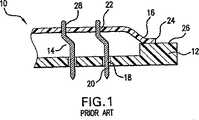
図1を参照して、従来技術として公知の座屈梁ダイ10の部分的に組み立てられた部分は、下部ダイ12、プローブ・ピン14及び組立補助フィルム16を備える。下部ダイ12は、プローブ先端部20が挿入される微小孔18の配列を含む。組立補助フィルム16は、フィルムに穴開けされた微小孔22と一致するパターンを含む。小さな組立補助フィルム16の一側縁24が、例えばテープ等を用いて下部ダイ12の上面26に接着されて、フィルムがほぼ微小孔18全体にわたって位置する。各プローブ先端部20が下部ダイの微小孔18の1つに挿入され、その際、プローブ頭部28が組立補助フィルム16の対応する微小孔22に挿入されて通り抜け、プローブ・ピン14を所定の位置に保持する。この工程は、各プローブ・ピン14が所定の位置に収まるまで継続される。プローブ頭部28の挿入は、各プローブ頭部をフィルムの下側に滑らかに押し進めて微小孔18の適当な1つを通り抜けるに十分な隙間を与えるように、組立補助フィルム16を持ち上げる必要がある。組立が進むと、組立補助フィルム16を周期的につなぎ止めて、既に孔に差し込まれた接点のプローブ頭部28から離れて持ち上がるのを防止する必要がある。それとは関係なく、組立補助フィルム16が時々プローブ頭部28から離れて持ち上がり、部分的又は完全な再組立が必要になる。組立補助フィルム16の微小孔22に通してプローブ頭部28を嵌入する工程は、また、各プローブ・ピン14が不用意に折り曲げられる機会を与える。 Referring to FIG. 1, a partially assembled portion of a buckled beam die 10 known in the prior art includes a
各プローブ・ピン14が、下部ダイ12及び組立補助フィルム16に装着された後、上部ダイの空洞内部に全体が収まるようにフィルムを切断し、つなぎ止めワイヤーを取り除く必要がある。この工程は、屡々組立補助フィルム16が1つ以上のプローブ頭部28から離れて持ち上がることになり、組立体の部分的又は完全な再組立を再び必要とする。組立補助フィルム16が切断され、ワイヤーが取り除かれた後、上部ダイ30を設置する必要がある。図2に示すように、これは、各プローブ頭部28が下部ダイの微小孔のそれぞれの1つにぴったりと合うように、プローブ・ピン14の配列の全体にわたって下部ダイ12及び組立補助フィルム16のそれぞれの微小孔18,22のパターンと一致した微小孔32の配列を有する、上部ダイ30を整合させる必要がある。これは、プローブ・ピンの折曲を避けるために、典型的には各数千のプローブ・ピン14が1つの微小孔32を同時に貫通しなければならないので、細心の注意を要する操作である。従って、組立を容易にするために、上部ダイ30の各微小孔32は、下部ダイ12及び組立補助フィルム16の微小孔より大きい。また、更に図2を参照して、上部ダイ30は、約0.1インチ(2.54mm)厚のポリイミド材料の円形ディスクから取り掛かり、微小孔32の配列を画定するパターンが孔開けされる0.010インチ(0.254mm)厚のオーダの薄い「ウェブ」を残しながら、空洞34を粉々に削り取る慣用の手段により作製される。削取り後の材料のバランスの崩れた内部応力や、吸湿等のため、配列を横断してかかる薄いウェブ材料を平らに保つことは屡々困難であり、上部ダイの比較的低い歩留まり率に帰す。 After each
上部ダイ30が設置された後、アライメントピン(図示せず)が挿入されて上部ダイを下部ダイ12と正しく合わせ、ネジ(図示せず)を取り付けて上部及び下部ダイを一緒に保持する。次に、配列の端から端まで整合したプローブ・ピン全体の長さに達するために、プローブ頭部28がラッピングされる。ラッピング工程のある帰結は、ラッピング破片が上部ダイ30の余分の大きさの微小孔32を通過し、頭部組立体内部の組立補助フィルム16に集まる、ということである。この破片は、導電性であり、接点間の電気的な短絡を避けるために除去されなければならない。従って、破片を適切に除去するために、ラッピング後に上部ダイ30を取り外す必要がある。上部ダイ30の取外しは、プローブ頭部28から離れて持ち上がる更なる機会を組立補助フィルム16に与え、組立体の部分的又は完全な再組立を必要とする。また、上部ダイ30は繰り返しとなる位置合わせ及び組立が必要であり、位置合わせが完全でないならば、プローブ・ピン14を折曲する別の機会を与える。 After the
座屈梁技術の1つの利点は修理能力にある。プローブ・ピンは試験用電子機器に永久に結合するものではないので、組立体全体を廃棄せずに損傷したプローブ・ピンを置き換えることが可能である。図2に示された従来の設計による修理工程には問題がある。修理工程は、プローブ・ピン14へのアクセスを得るために上部ダイ30を取り外す必要がある。次に、組立補助フィルム16を介して引っ張ることにより、損傷した1つのプローブ・ピン14が引き出され、同じ組立補助フィルムの孔を介して新たなプローブ・ピンが再び挿入される。上記技術を用いた時に生じることのある幾つかの問題がある。まず、上部ダイ30の取外しは、組立補助フィルム16を1つ以上のプローブ頭部から離して持ち上げることに繋がることがある。組立補助フィルム16が静電気で時々上部ダイ30の下側に付着して配列から完全に剥がれるようになり、完全な再組立が必要となる。 One advantage of buckled beam technology is its repair capability. Since the probe pins are not permanently coupled to the test electronics, it is possible to replace damaged probe pins without discarding the entire assembly. There is a problem with the repair process according to the conventional design shown in FIG. The repair process requires removal of the
上部ダイ30が首尾良く取り外されるならば、その時、組立補助フィルム16を介して損傷したあらゆるプローブ・ピン14を引き抜かなければならない。組立補助フィルム16の微小孔22は、例えば、典型的なプローブ・ピン14の直径よりも大きい0.0001インチ(0.00254mm)のオーダの直径をしていて「窮屈」であるので、プローブ・ピン「スエージ(金型の一種:swage)」がフィルムを通過できるように、組立補助フィルムを僅かに引き剥がさなければならない。組立補助フィルム16に対するこの「強い引っ張り」は、1つ以上のプローブ・ピン14から離して持ち上げる別の機会をフィルムに与える。
損傷した1つのプローブ・ピン14が首尾良く取り出され、別のプローブ・ピンが挿入されるならば、組立補助フィルム16の特定の1つの微小孔22が直ちに拡大されるが、新たなプローブ・ピンをその上部ダイ30の関連した微小孔32と位置合わせする際に潜在的な困難を引き起こす。また、組立補助フィルム16の拡大された1つの微小孔22は、プローブ・ピン14により自由な動きを可能にさせ、電気的短絡回路の形成に至る厳密な許容誤差の適用では、上記ピン14が隣接するプローブ・ピンに接触する可能性がある。If the
If one damaged
本発明の1つの態様は、ダイ・ヘッドの下部ダイ部分に形成された第一微小孔の第一配列にプローブ・ピンを整列させるダイ・ヘッドの上部ダイ部分にあり、第一表面が下部ダイ部分に接触するように構成された第一及び第二表面を有するスペーサ部分と、支持フレームと、第二表面と支持フレームの間に位置すると共に、プローブ・ピンを受け入れるように構成された第二微小孔の第二配列を備えた第一の組立補助フィルムとを含む。
本発明の別の態様は、ダイ・ヘッドにプローブ・ピンを整列させる整列機構を含むダイ・ヘッドにあって、複数の表面の少なくとも1つがプローブ・ピンを受け入れるように構成された第一微小孔の第一配列を備えた、複数の表面を有する下部ダイ部分と、スペーサ部分を備えた上部ダイ部分と、支持フレームと、第一の組立補助フィルムとを含み、スペーサ部分は、下部ダイ部分の複数の表面の少なくとも1つと接触する第一表面と、第二表面とを有し、第一の組立補助フィルムは、第二表面と支持フレームの間に位置し、プローブ・ピンを受け入れるように構成された第二微小孔の第二配列を備える。
本発明の更に別の態様は、ダイ・ヘッドの下部ダイ部分に形成された第一微小孔の第一配列にプローブ・ピンを整列させるダイ・ヘッドの上部ダイ部分にあり、第一表面が下部ダイ部分に接触するように構成された第一及び第二表面を有するスペーサ部分と、第二表面より上に位置する第一支持フレームと、プローブ・ピンを受け入れるように構成された第二微小孔の第二配列を備えた組立補助フィルムと、第一支持フレーム及び組立補助フィルムの上方に位置する第二支持フレームと、第二支持フレームに接合されると共に、プローブ・ピンを受け入れるように構成された第三微小孔の第三配列を備えたシートとを含む。One aspect of the invention resides in the upper die portion of the die head that aligns the probe pins with the first array of first microholes formed in the lower die portion of the die head, the first surface being the lower die. A spacer portion having first and second surfaces configured to contact the portion; a support frame; a second portion positioned between the second surface and the support frame and configured to receive a probe pin And a first assembly aid film having a second array of micropores.
Another aspect of the present invention is a die head that includes an alignment mechanism that aligns the probe pin with the die head, wherein at least one of the plurality of surfaces is configured to receive the probe pin. A lower die portion having a plurality of surfaces, a top die portion having a spacer portion, a support frame, and a first assembly aid film, wherein the spacer portion is a portion of the lower die portion. A first surface in contact with at least one of the plurality of surfaces and a second surface, wherein the first assembly aid film is located between the second surface and the support frame and configured to receive the probe pin A second array of second micropores formed.
Yet another aspect of the present invention resides in an upper die portion of a die head that aligns probe pins with a first array of first microholes formed in a lower die portion of the die head, the first surface being the lower surface. A spacer portion having first and second surfaces configured to contact the die portion; a first support frame positioned above the second surface; and a second microhole configured to receive the probe pin. And a second support frame positioned above the first support frame and the assembly support film, and joined to the second support frame and configured to receive the probe pins. And a sheet with a third array of third micropores.
本発明のまた更に別の態様は、上部及び下部部分を備えたダイ・ヘッドにプローブ・ピンを置き換える方法にあり、プローブ・ピンを把持する工程と、プローブ・ピンを上部及び下部部分から上向きに引っ張って、ダイ・ヘッドからプローブ・ピンを取り出す工程と、プローブ・ピンを上部及び下部部分の両方に通して下向きに挿入して、上記取出し工程で取り出されたプローブ・ピンと同じ箇所にプローブ・ピンを挿入する工程とを含む。
本発明のなお更に別の態様は、上部及び下部部分を備えたダイ・ヘッドにプローブ・ピンを組み立てる方法にあって、各々が微小孔の配列を備えた少なくとも1枚の組立補助フィルム及びシートの少なくとも1つを取り外す工程と、1つ以上のプローブ・ピンを上部及び下部部分の両方に通して下向きに挿入する工程と、上記取外し工程で取り外された少なくとも1枚の組立補助フィルム及びシートを置き換える工程とを含み、上記少なくとも1枚の組立補助フィルム及びシートは、微小孔の1つに各プローブ・ピンを入れて、プローブ・ピンの位置をダイ・ヘッドに維持する上部部分の上方に存在するように構成されており、ダイ・ヘッドに挿入された1つ以上のプローブ・ピンの各々は、微小孔の配列の1つにより包囲される。Yet another aspect of the invention resides in a method of replacing a probe pin with a die head having an upper and lower portion, the step of gripping the probe pin, and the probe pin being directed upward from the upper and lower portions. Pulling out the probe pin from the die head, inserting the probe pin downward through both the upper and lower parts, and inserting the probe pin into the same location as the probe pin taken out in the above extraction step Inserting.
Yet another aspect of the present invention is a method of assembling a probe pin to a die head having an upper and lower portion, comprising at least one assembly aid film and sheet each having an array of micropores. Removing at least one, inserting one or more probe pins downwardly through both the upper and lower portions, and replacing at least one assembly aid film and sheet removed in the removal step. And wherein the at least one assembly aid film and sheet are present above an upper portion that places each probe pin in one of the micropores and maintains the position of the probe pin on the die head. Each of the one or more probe pins inserted into the die head is surrounded by one of the arrays of micropores.
本発明を説明するために、図面は目下のところ好ましいとされる発明の形態を示す。しかし、本発明は、図面に示されたまさにその装置及び手段に限定されないことを理解すべきである。
さて、同じ参照番号が同じ部材又は部品を示す図3〜8、特に図3,4を参照して、本発明の一実施例は、ダイ・ヘッドの下部ダイ部分12に形成された第一微小孔18の第一配列にプローブ・ピン14を整列させるダイ・ヘッドの上部ダイ部分36を備える。上部ダイ部分36は、全体として、スペーサ部分38と、支持フレーム40と、それぞれ第一及び第二の組立補助フィルム42及び44とを備える。For the purpose of illustrating the invention, the drawings show an embodiment of the presently preferred invention. It should be understood, however, that the invention is not limited to the precise arrangements and instrumentalities shown in the drawings.
Referring now to FIGS. 3-8, in particular FIGS. 3 and 4, where the same reference numbers indicate the same members or parts, one embodiment of the present invention is the first micro-fabrication formed in the
スペーサ部分38は、それぞれ第一及び第二表面46及び48を有する。第一表面46は、下部ダイ部分12に接触するように構成される。スペーサ部分38は、典型的には断面が正方形又は直方形の環状形状をなし、例えば、繊維充填のエポキシ、低熱膨張率の金属又はセラミック等のダイ部分として好適であることが公知のあらゆる材料から形成されることができる。
支持フレーム40は、典型的には、例えばインバール(登録商標)のブランド名で販売されている低熱膨張率のニッケル合金等の金属箔から形成される。支持フレーム40は、典型的には形状がスペーサ38と同様であるが、各プローブ・ピン14の縦方向に関して寸法が小さい。
第一の組立補助フィルム42は、典型的には第二表面48と支持フレーム40の間に位置し、プローブ・ピン14を受け入れるように構成された第二微小孔50の第二配列を備える。第二の組立補助フィルム44は、概ね第一の組立補助フィルム42に接触又は近接近した状態にあり、プローブ・ピン14を受け入れるように構成された第三微小孔52の第三配列を備える。
The
The first
第二微小孔50の第二配列及び第三微小孔52の第三配列は、互いに整合しているが、下部ダイ12の第一微小孔18の第一配列とはズレてパターン化されている。ズレ(オフセット)量は、各プローブ・ピン14のオフセット量、即ちプローブ先端部20とプローブ頭部28間の横方向の距離によって定められる。第一の組立補助フィルム42における第二微小孔50の第二配列中の各微小孔は、概ねゆったりとした大きさをしており、例えば、典型的には直径がプローブ・ピン14の直径よりも大きく約0.5ミル(0.0005インチ(0.0127mm))であり、従来技術の上部ダイ30中の微小孔32(図2参照)よりは小さい。第二の組立補助フィルム44における第三微小孔52の第三配列中の各微小孔は、概ね第一の組立補助フィルム42の微小孔よりも小さく、例えば、典型的には直径が各プローブ・ピン14の直径よりも大きく約0.1ミル(0.0001インチ(0.00254mm))であるので、プローブ・ピンを互いに密接に関連した配列に保持することができ、各第三微小孔が効果的にシールされてダイ・ヘッドへの破片の混入を防止する。 The second array of
第一の組立補助フィルム42は、また、上部ダイ部分36の構成部材を下部ダイ12と位置合わせを行うダボ又は同様の構造物(図示せず)を嵌合することを目的とする位置合わせ孔54を備える。例えば3M 2290 Structural Adhesive(ミネソタ州セントポール所在の3M社製)等の市販の接着剤を用いて、第一の組立補助フィルム42を支持フレーム40とスペーサ部分38に結合することにより、上部ダイ部分36に更に構造上の剛性を高めることができる。
第一及び第二の組立補助フィルム42,44は、例えばポリイミドから形成される種類のあらゆる好適なポリマーフィルムであってもよく、典型的には双方とも少なくとも半透明である。第一の組立補助フィルム42は、全体的に穴56を横断するピンと張った「太鼓状膜(drum skin)」を作り出し、穴56はダイ・ヘッド及び支持フレーム40内に画定された周辺58を含み、それにより、従来の設計に特有の非平坦性という問題を解消する。第二の組立補助フィルム44は、概ね直径が第一の組立補助フィルム42よりも小さく、穴56の周辺58より小さい外周辺60を有する。そのため、第二の組立補助フィルム44は、典型的には支持フレーム40に接触せず、その代わり第一の組立補助フィルム42の上面に浮かぶことができる。The first
The first and second
さて、図5を参照して、代替の実施例において、上部ダイ部分36′は、典型的には外周辺60の周囲に設置される薄いシム62と、第二の組立補助フィルム44の上方、典型的にはシムの上面に位置するポリマーシート64とを備える。シム62は、典型的には、フィルム42の周辺に隣接する剛性の取付部分65に取り付けられることのできる第一の組立補助フィルム42の上面に設置される。取付部分65はスペーサ部分38の表面48の上面に置かれる。シム62は、全てのプローブ・ピンが装着され、第二の組立補助フィルムが上述の通り設置された後、第二の組立補助フィルム44の自由な動きを許容する。ポリマーシート64は上部ダイ部分36′に更なる剛性と安定性を与える。ポリマーシート64は、典型的には約6ミル(0.0152mm)厚のポリイミドから形成され、ゆったりとした大きさの、典型的には孔開けされた微小孔66を備える。位置合わせ孔54及びダボ・ピン(図示せず)を用いて、ポリマーシート64、スペーサ部分38及びシム62を位置合わせすることができる。ポリマーシート64はヘッドの修理のために取り外し可能であり、ネジ等を用いてシム62及びスペーサ38に取り付けることにより、シート64をきつく締め付けることができる。図5に図示の実施例において、下部ダイ部分12及び上部ダイ部分36′は、4つの微小孔の配列、即ち、第一微小孔18の第一配列、第二微小孔50の第二配列、第三微小孔66の第三配列及び第四微小孔52の第四配列を備える。 Referring now to FIG. 5, in an alternative embodiment, the
図6を参照して、別の実施例において、上部ダイ部分36″は、スペーサ部分38、第一支持フレーム67、組立補助フィルム68、第二支持フレーム70及びシート72を備える。スペーサ部分38は、それぞれ第一及び第二表面46及び48を有する。第一表面46は、下部ダイ部分12に接触するように構成される。第一支持フレーム67は、上記第二表面48に隣接して位置し、典型的には組立補助フィルム68をぴーんと張った状態に保持する。組立補助フィルム68は、プローブ・ピン14を受け入れるように構成された第二微小孔74の第二配列を備える。組立補助フィルム68は概ね少なくとも半透明である。第二支持フレーム70は、上記第一支持フレーム67及び上記組立補助フィルム68の上に位置する。シート72は、典型的には、第二支持フレーム70に接合され、プローブ・ピン14を受け入れるように構成された第三微小孔76の第三配列を備える。シート72は、典型的には約6ミル厚のポリイミドから形成される。第三微小孔76の第三配列は、典型的には余分の大きさを有しており、即ち、プローブ・ピン14の直径よりも大きい。前述の実施例と同じく、それぞれ第二及び第三配列74及び76は、第一配列18からズレるように構成される。 6, in another embodiment, the
さて、図7,8を参照して、本発明の別の実施例において、スペーサ部分38は、少なくとも、互いに切り離すことのできるそれぞれ第一及び第二部分38a及び38bを含んでいてもよく、スペーサ部分の引抜き及び挿入を容易にする。その際、第一の組立補助フィルム42を下部ダイ部分12に近接近させて、組立を行ってもよい。各プローブ先端部20は、組立補助フィルムの微小孔及び下部ダイ部分の微小孔を殆ど同時に通過する。さて、図8を参照して、全てのプローブ・ピン14が装着された後、接点(図示せず)の下部ダイ部分12からの持ち上がりを防止するために、接点の頭部全体にわたって位置するプレート102を有する固定具100にダイ・ヘッドが設置される。次に、第一の組立補助フィルム42を最終的な高さに持ち上げることができる。第一の組立補助フィルム42の持ち上げ工程は、全般的に全ての接点を整列させる。その後、スペーサの半分38a,38bが第一の組立補助フィルム42と下部ダイ部分12の間に挿入され、位置合わせ孔54を用いてダイ・ヘッド全体を一緒にピン留め及びネジ止めすることができる。 7 and 8, in another embodiment of the present invention, the
本発明の別の態様は、上部及び下部部分を備えたダイ・ヘッドにプローブ・ピンを置き換える方法にある。まず、シート64,72を取り外す。更に、存在するならば、微小孔の配列を備えた少なくとも1枚の組立補助フィルムを取り外す。次いで、ピンセット又は他の適当な大きさの道具を用いて、置き換えられるべきプローブ・ピン14のプローブ頭部28を把持する。次に、プローブ・ピンをそれぞれ上部及び下部部分36及び12から上向きに引っ張って、ダイ・ヘッドからそれぞれのプローブ・ピン14を取り出す。次に、それぞれ上部及び下部部分36及び12の両方に通してプローブ・ピンを下向きに挿入することにより、置換え用プローブ・ピン14を取り出されたプローブ・ピンと同じ箇所に挿入する。その後、存在するならば、先に取り外された少なくとも1枚の組立補助フィルムを置き換え、シート64,72を置き換える。 Another aspect of the invention resides in a method for replacing a probe pin with a die head having an upper and lower portion. First, the
本発明の更に別の態様は、ダイ・ヘッドにプローブ・ピン14を組み立てる方法にある。ネジ、ダボ等を用いて、上部ダイ部分36を下部ダイ部分12に固着した後、各プローブ先端部20及びプローブ・ピン本体を組立補助フィルム(42又は68)のゆったりとした大きさの微小孔に、次いで下部ダイの対応する微小孔18内に通して、各プローブ・ピン14を装着する。各組立補助フィルムは好ましくは少なくとも半透明であるので、組立補助フィルムを介して下部ダイの各微小孔18を見ることが可能であり、それによって、組立が容易になる。2枚以上の組立補助シートを用いるか又はポリマーシートを利用する実施の形態では、各プローブ・ピン14を残りの組立補助シートに通して下部ダイ部分12の対応する微小孔18内に挿入する前に、ポリマーシート及び組立補助シートの双方を取り外してもよい。次に、各プローブ頭部28を取り外された組立補助フィルム及びポリマーシートの対応する微小孔に通しながら、組立補助フィルム及びポリマーシートを装着されたプローブ・ピンの頂部に配置する。 Yet another aspect of the invention resides in a method for assembling probe pins 14 to a die head. After the
本発明は、従来技術の設計より優れた複数の利益及び利点を提供する。例えば、本発明の設計はダイ・ヘッドの修理能力を向上させる。単に、第二の組立補助フィルム及び/又はポリイミド・シートを取り外し、損傷したプローブ・ピンを第一の組立補助フィルムのゆったりとした大きさの微小孔に通して引き抜き、新たなプローブ・ピンを再挿入し、第二の組立補助フィルムを再び取り付けるだけで、修理を行うことができる。上部ダイを取り外す必要性がなく、組立補助フィルムがプローブ頭部から離れて持ち上がる可能性がなく、フィルムの引き剥がしがない。
上述の本発明の組立工程は、従来技術の組立工程より優れた幾つかの利益を提供する。まず、一般に従来の組立に要する時間の約1/3で組立工程を完了できる。次に、もはや組立補助フィルムをつなぎ止める必要がないので、フィルムがプローブ頭部から離れて持ち上がる可能性がない。また、もはやプローブ頭部を折り曲げ、組立補助フィルムに通して上向きに挿入する必要がないので、プローブ・ピンを折り曲げる可能性がかなり減少する。The present invention provides several benefits and advantages over prior art designs. For example, the design of the present invention improves the repair capability of the die head. Simply remove the second assembly aid film and / or polyimide sheet, pull the damaged probe pin through the loose sized hole in the first assembly aid film, and re-install the new probe pin. Repair can be done by simply inserting and reattaching the second assembly aid film. There is no need to remove the upper die, there is no possibility that the assembly auxiliary film will be lifted away from the probe head, and there is no film peeling.
The assembly process of the present invention described above provides several advantages over prior art assembly processes. First, the assembly process can be completed in about 1/3 of the time required for conventional assembly. Secondly, there is no possibility that the film lifts away from the probe head because there is no longer any need to anchor the assembly aid film. Also, since the probe head no longer has to be folded and inserted upward through the assembly aid film, the possibility of bending the probe pin is significantly reduced.
先に本発明の一実施例で説明したように、全てのプローブ・ピンが装着された後、より小さな直径の微小孔の配列を備えた第二の組立補助フィルムが、プローブ頭部全体にわたって位置合わせされ、第一の組立補助フィルムの表面に下げられる。より小さな微小孔は、プローブ・ピンが互いに密接に関連した配列状態に保持することを可能にさせる。更に、第二の組立補助フィルムは、通常ダイ組立体に固定されていないので、プローブ・ピンの圧縮中に、なおその相対的な位置を維持しながらプローブ・ピンの自由な動きを許容する。プローブ・ピンに対する第二の組立補助フィルムの位置合わせは、従来の設計における上部ダイの位置合わせよりも非常に簡単である。というのは、a)第二の組立補助フィルムが好ましくは少なくとも半透明であるので、プローブ・ピンは常に視認可能であり、b)全てのプローブ・ピンが必ずしも配列中の全ての微小孔を同時に通過する必要がなく、むしろ、第二の組立補助フィルムを配列部分に段階的に当てはめることができるからである。 As previously described in one embodiment of the present invention, after all probe pins have been installed, a second assembly aid film with an array of smaller diameter micro-holes is located throughout the probe head. Combined and lowered to the surface of the first assembly aid film. Smaller micropores allow the probe pins to be kept in an closely related arrangement. Further, since the second assembly aid film is not normally secured to the die assembly, it allows free movement of the probe pin during compression of the probe pin while still maintaining its relative position. The alignment of the second assembly aid film with respect to the probe pins is much simpler than the alignment of the upper die in the conventional design. This is because a) the second assembly aid film is preferably at least translucent so that the probe pins are always visible, and b) all probe pins do not necessarily have all the micropores in the array simultaneously. It is not necessary to pass through, but rather, the second assembly aid film can be applied stepwise to the array portion.
第二の組立補助フィルムの更なる利点はラッピング工程で明らかになる。かなり先に説明したように、ラッピング工程では破片が発生する。第二の組立補助フィルムがより小さな直径の、即ち「窮屈な」微小孔を備えているので、ラッピングした破片は、頭部組立体内を通るというよりは、むしろ上記フィルムの上面に集まる。破片が組立体の外部にあると、上部ダイを取り外すことなく容易に取り出せる。第二の組立補助フィルムさえも全体を取り外して、清浄なフィルムと置き換えることができる。 Further advantages of the second assembly aid film become apparent during the lapping process. As explained earlier, debris is generated in the lapping process. Because the second assembly aid film has smaller diameter or “tight” micropores, the lapped debris collects on the top surface of the film rather than passing through the head assembly. If the debris is outside the assembly, it can be easily removed without removing the upper die. Even the second assembly aid film can be removed entirely and replaced with a clean film.
本発明は、また、熱膨張領域における従来技術の設計より優れた改良を提供する。高温試験の応用では、下部及び上部ダイは、プローブ・ピンとこれらが接触するパッドの間の配置構造を維持するために、低熱膨張係数(CTE)の材料から構成される。パッドは典型的には低いCTEの材料に位置する。低いCTEの材料は、従来のポリイミド材料と比較して、微小な孔開けに関して課題を提示するかも知れない。本発明では、第一の組立体取付フィルムが、インバール(登録商標)等のブランド名で販売されているようなものなど、低いCTEの金属箔に結合される。ポリイミド・フィルムはCTEがより高い。しかし、フィルムは、例えば1ミルと、非常に薄いので、圧縮力を支持することができない。従って、フィルムが膨張すると接点を離間させることができず、ズレを引き起こすというより、むしろ僅かに垂れ下がり、上部ダイについてCTEの不一致という問題を緩和する。 The present invention also provides an improvement over prior art designs in the thermal expansion region. In high temperature test applications, the lower and upper dies are constructed from a low coefficient of thermal expansion (CTE) material to maintain the arrangement between the probe pins and the pads with which they contact. The pad is typically located on a low CTE material. Low CTE materials may present challenges with respect to micro-drilling compared to conventional polyimide materials. In the present invention, the first assembly mounting film is bonded to a low CTE metal foil, such as that sold under a brand name such as Invar®. Polyimide films have a higher CTE. However, the film is so thin, for example 1 mil, that it cannot support the compressive force. Thus, as the film expands, the contacts cannot be spaced apart, rather than causing misalignment, rather sag slightly and alleviate the problem of CTE mismatch for the upper die.
本発明の孔開け加工は、また、従来技術の加工より優れた改良を提供する。高品質の微小孔を実現すると共にドリルによる破損を避けるために、孔開け加工は制御された送り速度及び多数のパス(通り過ぎること)を必要とするので、従来の上部ダイの孔開けには時間がかかる。これに反し、本発明の組立補助フィルムは、低コストかつ短い準備時間でパンチングによる穴開け又はレーザによる孔開けを行うことができる。また、本発明のフィルムは、非常に窮屈なピッチの適用に利点をもたらす長穴の形成の機会を提供するが、一方、従来の孔開け加工は典型的には丸穴に限定される。 The drilling process of the present invention also provides an improvement over prior art processes. In order to achieve high quality micro holes and to avoid breakage due to drilling, the drilling process requires a controlled feed rate and multiple passes (passing), so the time required for conventional top die drilling is time consuming. It takes. On the other hand, the assembly auxiliary film of the present invention can perform punching by punching or laser drilling at low cost and with short preparation time. Also, the film of the present invention provides an opportunity for slotted hole formation that provides advantages for very tight pitch applications, while conventional drilling is typically limited to round holes.
本発明をその代表的な実施例に関して説明及び図示したが、当業者であれば、本発明の精神及び範囲から逸脱することなく、本発明中に及び本発明に対して、前述の及びその他様々な変化や、省略、並びに追加を行ってもよいことを理解すべきである。 While the invention has been described and illustrated with reference to exemplary embodiments thereof, those skilled in the art will recognize that the foregoing and various other arrangements may be made within and with respect to the invention without departing from the spirit and scope of the invention. It should be understood that various changes, omissions, and additions may be made.
Claims (10)
Translated fromJapanese第一及び第二表面(46,48)を有し、第一表面(46)が前記下部ダイ部分(12)に接触するように構成されたスペーサ部分(38)と、
支持フレーム(40)と、
前記第二表面(48)と前記支持フレーム(40)の間に加圧下に取り付けられ、プローブ・ピン(14)を受け入れるように構成されて軸線方向又は横方向の動きを阻止され、第二微小孔(50)の第二配列を備えた、第一の組立補助フィルム(42)と、
前記第一の組立補助フィルム(42)に近接し、前記プローブ・ピン(14)を受け入れるように構成された第三微小孔(52)の第三配列を備えた、第二の組立補助フィルム(44)と、
前記第三微小孔(52)の第三配列外周辺(60)の周囲の薄いシム(62)と、
余分の大きさの微小孔(66)を備え、前記第二の組立補助フィルム(44)の上面部に位置するシート(64)と、
をふくむ、上部ダイ部分(36)。A die head that aligns the probe pins (14) with the first array of first micro-holes (18) formed in the upper die portion (36) of the die head, the lower die portion (12) of the die head. In the upper die part (36) of the head,
A spacer portion (38) having first and second surfaces (46, 48), wherein the first surface (46) is configured to contact the lower die portion (12);
A support frame (40);
Mounted under pressure between the second surface (48) and the support frame (40) and configured to receive a probe pin (14) to prevent axial or lateral movement, the second micro A first assembly aid film (42) with a second array of holes (50);
A second assembly aid film (3) comprising a third array of third micropores (52) configured to receive the probe pins (14) proximate to the first assembly aid film (42). 44)
A thin shim (62) around the outer periphery (60) of the third array of the third micropores (52);
A sheet (64) provided with an extra-sized microhole (66) and positioned on the upper surface of the second assembly auxiliary film (44);
Including the upper die part (36).
第一及び第二表面(46,48)を有し、第一表面(46)が前記下部ダイ部分(12)に接触するように構成されたスペーサ部分(38)と、
前記第二表面(48)より上に位置する第一支持フレーム(67)と、
前記プローブ・ピン(14)を受け入れるように構成された第二微小孔(74)の第二配列を備えた組立補助フィルム(68)と、
前記第一支持フレーム(67)及び前記組立補助フィルム(68)より上に位置する第二支持フレーム(70)と、
前記第二支持フレーム(70)に接合され、前記プローブ・ピン(14)を受け入れるように構成された第三微小孔(76)の第三配列を備えたシート(72)とを含み、
前記組立補助フィルム(68)は軸線方向又は横方向の動きを阻止する
上部ダイ部分(36)。A die head that aligns the probe pins (14) with the first array of first micro-holes (18) formed in the upper die portion (36) of the die head, the lower die portion (12) of the die head. In the upper die part (36) of the head,
A spacer portion (38) having first and second surfaces (46, 48), wherein the first surface (46) is configured to contact the lower die portion (12);
A first support frame (67) located above the second surface (48);
An assembly aid film (68) with a second array of second micropores (74) configured to receive the probe pins (14);
A second support frame (70) positioned above the first support frame (67) and the assembly auxiliary film (68);
A sheet (72) with a third array of third micropores (76) joined to the second support frame (70) and configured to receive the probe pins (14);
The assembly assisting film (68) is an upper die portion (36) that prevents axial or lateral movement.
Applications Claiming Priority (3)
| Application Number | Priority Date | Filing Date | Title |
|---|---|---|---|
| US51996603P | 2003-11-14 | 2003-11-14 | |
| US60/519,966 | 2003-11-14 | ||
| PCT/US2004/037953WO2005050706A2 (en) | 2003-11-14 | 2004-11-12 | Die design with integrated assembly aid |
Publications (2)
| Publication Number | Publication Date |
|---|---|
| JP2007512516A JP2007512516A (en) | 2007-05-17 |
| JP4732360B2true JP4732360B2 (en) | 2011-07-27 |
Family
ID=34619404
Family Applications (1)
| Application Number | Title | Priority Date | Filing Date |
|---|---|---|---|
| JP2006539943AExpired - Fee RelatedJP4732360B2 (en) | 2003-11-14 | 2004-11-12 | Die design with assembly aids |
Country Status (9)
| Country | Link |
|---|---|
| US (2) | US7282936B2 (en) |
| EP (1) | EP1692529A4 (en) |
| JP (1) | JP4732360B2 (en) |
| KR (1) | KR101147032B1 (en) |
| CN (1) | CN100595598C (en) |
| CR (1) | CR8438A (en) |
| MY (1) | MY137372A (en) |
| TW (1) | TWI375798B (en) |
| WO (1) | WO2005050706A2 (en) |
Cited By (1)
| Publication number | Priority date | Publication date | Assignee | Title |
|---|---|---|---|---|
| JP2538424Y2 (en) | 1986-07-28 | 1997-06-18 | アエロスパシアル、ソシエテ、ナショナル、アンデュストリエル | Rotary wing aircraft blade |
Families Citing this family (24)
| Publication number | Priority date | Publication date | Assignee | Title |
|---|---|---|---|---|
| US7609512B2 (en)* | 2001-11-19 | 2009-10-27 | Otter Products, Llc | Protective enclosure for electronic device |
| US7649372B2 (en)* | 2003-11-14 | 2010-01-19 | Wentworth Laboratories, Inc. | Die design with integrated assembly aid |
| TWI261933B (en)* | 2005-11-21 | 2006-09-11 | Mjc Probe Inc | Method for batch production process of micro-hole guide plate of vertical probe card |
| DE202007016398U1 (en)* | 2006-11-27 | 2008-02-21 | Feinmetall Gmbh | Contacting device for contacting an electrical DUT to be tested |
| US7554348B2 (en)* | 2007-06-29 | 2009-06-30 | Wentworth Laboratories, Inc. | Multi-offset die head |
| US8664969B2 (en)* | 2009-09-11 | 2014-03-04 | Probelogic, Inc. | Methods and apparatus for implementing electrical connectivity for electronic circuit testing |
| US8217674B2 (en)* | 2010-02-08 | 2012-07-10 | Texas Instruments Incorporated | Systems and methods to test integrated circuits |
| CN102346201B (en)* | 2010-07-26 | 2015-06-17 | 旺矽科技股份有限公司 | Probe head of vertical probe card and manufacturing method thereof |
| TWI435083B (en)* | 2010-07-27 | 2014-04-21 | Mpi Corp | Combination probe head for vertical probe card and its assembly alignment method |
| WO2012078944A1 (en)* | 2010-12-09 | 2012-06-14 | Wentworth Laboratories, Inc. | Probe card assemblies and probe pins including carbon nanotubes |
| CN103245807B (en)* | 2012-02-06 | 2015-11-25 | 景美科技股份有限公司 | Probe unit structure and manufacturing method thereof |
| KR101366036B1 (en) | 2012-11-02 | 2014-02-28 | (주) 루켄테크놀러지스 | Vertical type probe card |
| JP6112890B2 (en)* | 2013-02-07 | 2017-04-12 | 日置電機株式会社 | Probe unit, board inspection apparatus, and probe unit assembling method |
| ITMI20130561A1 (en)* | 2013-04-09 | 2014-10-10 | Technoprobe Spa | HEAD OF MEASUREMENT OF ELECTRONIC DEVICES |
| KR101437774B1 (en) | 2013-04-17 | 2014-09-11 | 송지은 | Advanced Probe Head |
| KR101476683B1 (en)* | 2013-05-08 | 2014-12-26 | (주) 루켄테크놀러지스 | Vertical film type probe card |
| TWI521212B (en)* | 2014-03-10 | 2016-02-11 | A method and a method of assembling a vertical probe device, and a vertical probe device | |
| KR20170092523A (en)* | 2014-12-04 | 2017-08-11 | 테크노프로브 에스.피.에이. | Testing head comprising vertical probes |
| US9535091B2 (en)* | 2015-03-16 | 2017-01-03 | Taiwan Semiconductor Manufacturing Co., Ltd. | Probe head, probe card assembly using the same, and manufacturing method thereof |
| JP2018179721A (en)* | 2017-04-12 | 2018-11-15 | 株式会社日本マイクロニクス | Electrical connection device |
| TWI640783B (en)* | 2017-09-15 | 2018-11-11 | 中華精測科技股份有限公司 | Probe card device and round probe |
| IT202000028838A1 (en)* | 2020-11-27 | 2022-05-27 | Technoprobe Spa | LARGE MEASUREMENT CARD FOR TESTING ELECTRONIC DEVICES AND RELATED MANUFACTURING METHOD |
| US12332291B2 (en)* | 2021-07-30 | 2025-06-17 | Taiwan Semiconductor Manufacturing Company Ltd. | Method for probe pin retrieval |
| KR102817547B1 (en)* | 2022-03-31 | 2025-06-10 | 재팬 일렉트로닉 메트리얼스 코오포레이숀 | Probe insertion method and probe |
Family Cites Families (60)
| Publication number | Priority date | Publication date | Assignee | Title |
|---|---|---|---|---|
| JPS5065232A (en) | 1973-10-09 | 1975-06-02 | ||
| JPS5230848B2 (en) | 1973-10-09 | 1977-08-11 | ||
| US4027935A (en) | 1976-06-21 | 1977-06-07 | International Business Machines Corporation | Contact for an electrical contactor assembly |
| FR2493671A1 (en)* | 1980-10-30 | 1982-05-07 | Everett Charles Inc | CONTACTS SHIFT, TEST APPARATUS WITH CONTACTS SHIFT, AND METHOD FOR MANUFACTURING CONTACTS SHIFT |
| DE3175044D1 (en) | 1981-10-30 | 1986-09-04 | Ibm Deutschland | Test apparatus for testing runs of a circuit board with at least one test head comprising a plurality of flexible contacts |
| US4451327A (en) | 1982-12-17 | 1984-05-29 | Psi Star, Inc. | Process and structure for etching copper |
| US4466859A (en) | 1983-05-25 | 1984-08-21 | Psi Star, Inc. | Process for etching copper |
| US6043563A (en) | 1997-05-06 | 2000-03-28 | Formfactor, Inc. | Electronic components with terminals and spring contact elements extending from areas which are remote from the terminals |
| US5917707A (en) | 1993-11-16 | 1999-06-29 | Formfactor, Inc. | Flexible contact structure with an electrically conductive shell |
| US5829128A (en) | 1993-11-16 | 1998-11-03 | Formfactor, Inc. | Method of mounting resilient contact structures to semiconductor devices |
| US4747907A (en) | 1986-10-29 | 1988-05-31 | International Business Machines Corporation | Metal etching process with etch rate enhancement |
| US4901013A (en)* | 1988-08-19 | 1990-02-13 | American Telephone And Telegraph Company, At&T Bell Laboratories | Apparatus having a buckling beam probe assembly |
| US4980638A (en) | 1989-05-26 | 1990-12-25 | Dermon John A | Microcircuit probe and method for manufacturing same |
| JPH0362546A (en) | 1989-07-31 | 1991-03-18 | Toshiba Corp | Scanning probe and manufacture thereof |
| US5415559A (en)* | 1992-05-18 | 1995-05-16 | Japan Aviation Electronics Industry, Ltd. | Electrical connector having a plurality of contact pin springs |
| JPH0650991A (en)* | 1992-07-31 | 1994-02-25 | Toho Denshi Kk | Probe apparatus |
| JPH06249878A (en) | 1993-03-01 | 1994-09-09 | Kobe Steel Ltd | Probe unit and manufacture thereof |
| US5326428A (en) | 1993-09-03 | 1994-07-05 | Micron Semiconductor, Inc. | Method for testing semiconductor circuitry for operability and method of forming apparatus for testing semiconductor circuitry for operability |
| US6023103A (en) | 1994-11-15 | 2000-02-08 | Formfactor, Inc. | Chip-scale carrier for semiconductor devices including mounted spring contacts |
| US5508144A (en) | 1993-11-19 | 1996-04-16 | At&T Corp. | Process for fabricating a device |
| US5493230A (en) | 1994-02-25 | 1996-02-20 | Everett Charles Technologies, Inc. | Retention of test probes in translator fixtures |
| US5416429A (en) | 1994-05-23 | 1995-05-16 | Wentworth Laboratories, Inc. | Probe assembly for testing integrated circuits |
| US5495667A (en) | 1994-11-07 | 1996-03-05 | Micron Technology, Inc. | Method for forming contact pins for semiconductor dice and interconnects |
| US6150186A (en) | 1995-05-26 | 2000-11-21 | Formfactor, Inc. | Method of making a product with improved material properties by moderate heat-treatment of a metal incorporating a dilute additive |
| KR0150334B1 (en)* | 1995-08-17 | 1998-12-01 | 남재우 | Probe card having vertical needle |
| KR970053345A (en)* | 1995-12-30 | 1997-07-31 | 김광호 | Carrier Transfer Device |
| US5883520A (en)* | 1996-06-14 | 1999-03-16 | Star Technology Group, Inc. | Retention of test probes in translator fixtures |
| JP2972595B2 (en)* | 1996-09-25 | 1999-11-08 | 日本電気ファクトリエンジニアリング株式会社 | Probe card |
| US5977787A (en) | 1997-06-16 | 1999-11-02 | International Business Machines Corporation | Large area multiple-chip probe assembly and method of making the same |
| US5959461A (en) | 1997-07-14 | 1999-09-28 | Wentworth Laboratories, Inc. | Probe station adapter for backside emission inspection |
| WO1999004273A1 (en) | 1997-07-15 | 1999-01-28 | Wentworth Laboratories, Inc. | Probe station with multiple adjustable probe supports |
| JPH11125646A (en) | 1997-10-21 | 1999-05-11 | Mitsubishi Electric Corp | Vertical needle probe card, method of manufacturing the same, and method of replacing defective probe needle |
| ATE260470T1 (en)* | 1997-11-05 | 2004-03-15 | Feinmetall Gmbh | TEST HEAD FOR MICROSTRUCTURES WITH INTERFACE |
| JPH11160356A (en) | 1997-11-25 | 1999-06-18 | Matsushita Electric Ind Co Ltd | Probe card for wafer batch type measurement / inspection, ceramic multilayer wiring board, and manufacturing method thereof |
| SE518084C2 (en)* | 1998-01-23 | 2002-08-20 | Ericsson Telefon Ab L M | Processes and devices related to functions or functional devices and methods for controlling the process flow between functions |
| US5952843A (en) | 1998-03-24 | 1999-09-14 | Vinh; Nguyen T. | Variable contact pressure probe |
| US6194127B1 (en) | 1998-05-27 | 2001-02-27 | Mcdonnell Douglas Corporation | Resistive sheet patterning process and product thereof |
| JPH11344509A (en)* | 1998-05-29 | 1999-12-14 | Hiroshi Katagawa | Probe card and probe pin |
| US6503231B1 (en) | 1998-06-10 | 2003-01-07 | Georgia Tech Research Corporation | Microneedle device for transport of molecules across tissue |
| US6303262B1 (en) | 1998-06-18 | 2001-10-16 | Mitsubishi Paper Mills Ltd. | Photomask material, photomask and methods for the production thereof |
| JP3443011B2 (en)* | 1998-08-20 | 2003-09-02 | シャープ株式会社 | Film carrier tape and test method therefor |
| US6124723A (en) | 1998-08-31 | 2000-09-26 | Wentworth Laboratories, Inc. | Probe holder for low voltage, low current measurements in a water probe station |
| US6160412A (en) | 1998-11-05 | 2000-12-12 | Wentworth Laboratories, Inc. | Impedance-matched interconnection device for connecting a vertical-pin integrated circuit probing device to integrated circuit test equipment |
| SG75186A1 (en)* | 1998-11-30 | 2000-09-19 | Advantest Corp | Method for producing contact structures |
| US6297657B1 (en) | 1999-01-11 | 2001-10-02 | Wentworth Laboratories, Inc. | Temperature compensated vertical pin probing device |
| US6163162A (en) | 1999-01-11 | 2000-12-19 | Wentworth Laboratories, Inc. | Temperature compensated vertical pin probing device |
| US6404211B2 (en) | 1999-02-11 | 2002-06-11 | International Business Machines Corporation | Metal buckling beam probe |
| US6255602B1 (en) | 1999-03-15 | 2001-07-03 | Wentworth Laboratories, Inc. | Multiple layer electrical interface |
| US6330744B1 (en) | 1999-07-12 | 2001-12-18 | Pjc Technologies, Inc. | Customized electrical test probe head using uniform probe assemblies |
| JP2001099863A (en)* | 1999-10-01 | 2001-04-13 | Japan Electronic Materials Corp | Probe and probe card using the same |
| US6363605B1 (en) | 1999-11-03 | 2002-04-02 | Yi-Chi Shih | Method for fabricating a plurality of non-symmetrical waveguide probes |
| FR2802346B1 (en) | 1999-12-13 | 2002-02-08 | Upsys Probe Technology Sas | HIGH INTERCONNECTION DENSITY TEST CONNECTOR, IN PARTICULAR FOR VERIFYING INTEGRATED CIRCUITS |
| US6633175B1 (en)* | 2000-03-06 | 2003-10-14 | Wenworth Laboratories, Inc. | Temperature compensated vertical pin probing device |
| JP3486841B2 (en) | 2000-08-09 | 2004-01-13 | 日本電子材料株式会社 | Vertical probe card |
| US6564454B1 (en) | 2000-12-28 | 2003-05-20 | Amkor Technology, Inc. | Method of making and stacking a semiconductor package |
| US6448506B1 (en) | 2000-12-28 | 2002-09-10 | Amkor Technology, Inc. | Semiconductor package and circuit board for making the package |
| WO2002061443A1 (en)* | 2001-01-31 | 2002-08-08 | Wentworth Laboratories, Inc. | Nickel alloy probe card frame laminate |
| US6573734B2 (en) | 2001-05-08 | 2003-06-03 | The Board Of Trustees Of The University Of Illinois | Integrated thin film liquid conductivity sensor |
| US6906540B2 (en)* | 2001-09-20 | 2005-06-14 | Wentworth Laboratories, Inc. | Method for chemically etching photo-defined micro electrical contacts |
| JP2003234359A (en)* | 2002-02-08 | 2003-08-22 | Hitachi Ltd | Method for manufacturing semiconductor device |
- 2004
- 2004-11-12CNCN200480033430Apatent/CN100595598C/ennot_activeExpired - Lifetime
- 2004-11-12EPEP04810930.0Apatent/EP1692529A4/ennot_activeWithdrawn
- 2004-11-12WOPCT/US2004/037953patent/WO2005050706A2/enactiveSearch and Examination
- 2004-11-12KRKR1020067011744Apatent/KR101147032B1/ennot_activeExpired - Fee Related
- 2004-11-12JPJP2006539943Apatent/JP4732360B2/ennot_activeExpired - Fee Related
- 2004-11-12USUS10/987,039patent/US7282936B2/ennot_activeExpired - Lifetime
- 2004-11-12MYMYPI20044742Apatent/MY137372A/enunknown
- 2004-11-15TWTW093134933Apatent/TWI375798B/ennot_activeIP Right Cessation
- 2006
- 2006-06-07CRCR8438Apatent/CR8438A/ennot_activeApplication Discontinuation
- 2007
- 2007-10-15USUS11/872,433patent/US7388392B2/ennot_activeExpired - Lifetime
Cited By (1)
| Publication number | Priority date | Publication date | Assignee | Title |
|---|---|---|---|---|
| JP2538424Y2 (en) | 1986-07-28 | 1997-06-18 | アエロスパシアル、ソシエテ、ナショナル、アンデュストリエル | Rotary wing aircraft blade |
Also Published As
| Publication number | Publication date |
|---|---|
| US20050110510A1 (en) | 2005-05-26 |
| TWI375798B (en) | 2012-11-01 |
| US7282936B2 (en) | 2007-10-16 |
| EP1692529A4 (en) | 2014-03-26 |
| US20080084227A1 (en) | 2008-04-10 |
| WO2005050706A3 (en) | 2005-12-29 |
| KR101147032B1 (en) | 2012-05-22 |
| CN100595598C (en) | 2010-03-24 |
| CR8438A (en) | 2006-09-22 |
| US7388392B2 (en) | 2008-06-17 |
| JP2007512516A (en) | 2007-05-17 |
| CN1879025A (en) | 2006-12-13 |
| MY137372A (en) | 2009-01-30 |
| WO2005050706A2 (en) | 2005-06-02 |
| TW200530591A (en) | 2005-09-16 |
| EP1692529A2 (en) | 2006-08-23 |
| KR20060135665A (en) | 2006-12-29 |
Similar Documents
| Publication | Publication Date | Title |
|---|---|---|
| JP4732360B2 (en) | Die design with assembly aids | |
| US7649372B2 (en) | Die design with integrated assembly aid | |
| US7898272B2 (en) | Probe card | |
| TWI451093B (en) | Multi-offset die head | |
| KR100690235B1 (en) | Chemically Etched Photo-Define Micro-Electric Contacts | |
| JP4439203B2 (en) | Multi-face mask device and assembly method thereof | |
| KR101138217B1 (en) | Method for forming photo-defined micro electrical contacts | |
| JP2010038900A (en) | Method of manufacturing mems probe available for probe card to reusable substrate | |
| US7046021B2 (en) | Double acting spring probe | |
| KR101610448B1 (en) | Probe card and method for manufacturing same | |
| JP2008151573A (en) | Electrical connection device and manufacturing method thereof | |
| JP4125598B2 (en) | Nickel alloy probe card frame laminate | |
| TW201304093A (en) | Microsprings at least partially embedded in a laminate structure and methods for producing same | |
| KR20070117974A (en) | Micro probe manufacturers | |
| KR101423376B1 (en) | Align hole having Probe pins including a flame formed in the Probe head | |
| JP2021005522A (en) | Anisotropic conductive sheet with frame, manufacturing method thereof, and usage thereof | |
| KR100830138B1 (en) | Conductive contact holder, conductive contact unit and process for producing conductive contact holder | |
| JP5913244B2 (en) | Mold release device | |
| JP4920818B2 (en) | Punching device and punching system | |
| JP5354615B2 (en) | Punching device and punching system | |
| JP2006159264A (en) | Laser beam machining tool, laser beam machining apparatus using the tool, and manufacturing method of multilayer ceramic electronic component | |
| JP2007171138A (en) | Probe, probe card, probe manufacturing method, and method for manufacturing probe support substrate | |
| JP2013190367A (en) | Method for manufacturing membrane probe | |
| JPH0922840A (en) | Method and apparatus for forming outer electrode of electronic component | |
| JP2016102802A (en) | Method of fixing sheet and ring |
Legal Events
| Date | Code | Title | Description |
|---|---|---|---|
| A621 | Written request for application examination | Free format text:JAPANESE INTERMEDIATE CODE: A621 Effective date:20071108 | |
| A977 | Report on retrieval | Free format text:JAPANESE INTERMEDIATE CODE: A971007 Effective date:20100419 | |
| A131 | Notification of reasons for refusal | Free format text:JAPANESE INTERMEDIATE CODE: A131 Effective date:20100423 | |
| A601 | Written request for extension of time | Free format text:JAPANESE INTERMEDIATE CODE: A601 Effective date:20100723 | |
| A602 | Written permission of extension of time | Free format text:JAPANESE INTERMEDIATE CODE: A602 Effective date:20100730 | |
| A601 | Written request for extension of time | Free format text:JAPANESE INTERMEDIATE CODE: A601 Effective date:20100823 | |
| A602 | Written permission of extension of time | Free format text:JAPANESE INTERMEDIATE CODE: A602 Effective date:20100830 | |
| A601 | Written request for extension of time | Free format text:JAPANESE INTERMEDIATE CODE: A601 Effective date:20100924 | |
| A602 | Written permission of extension of time | Free format text:JAPANESE INTERMEDIATE CODE: A602 Effective date:20101001 | |
| A521 | Request for written amendment filed | Free format text:JAPANESE INTERMEDIATE CODE: A523 Effective date:20101022 | |
| A131 | Notification of reasons for refusal | Free format text:JAPANESE INTERMEDIATE CODE: A131 Effective date:20101109 | |
| A601 | Written request for extension of time | Free format text:JAPANESE INTERMEDIATE CODE: A601 Effective date:20110209 | |
| A602 | Written permission of extension of time | Free format text:JAPANESE INTERMEDIATE CODE: A602 Effective date:20110217 | |
| A601 | Written request for extension of time | Free format text:JAPANESE INTERMEDIATE CODE: A601 Effective date:20110309 | |
| A602 | Written permission of extension of time | Free format text:JAPANESE INTERMEDIATE CODE: A602 Effective date:20110316 | |
| A521 | Request for written amendment filed | Free format text:JAPANESE INTERMEDIATE CODE: A523 Effective date:20110318 | |
| A01 | Written decision to grant a patent or to grant a registration (utility model) | Free format text:JAPANESE INTERMEDIATE CODE: A01 Effective date:20110408 | |
| A01 | Written decision to grant a patent or to grant a registration (utility model) | Free format text:JAPANESE INTERMEDIATE CODE: A01 | |
| A61 | First payment of annual fees (during grant procedure) | Free format text:JAPANESE INTERMEDIATE CODE: A61 Effective date:20110420 | |
| FPAY | Renewal fee payment (event date is renewal date of database) | Free format text:PAYMENT UNTIL: 20140428 Year of fee payment:3 | |
| R150 | Certificate of patent or registration of utility model | Free format text:JAPANESE INTERMEDIATE CODE: R150 | |
| R250 | Receipt of annual fees | Free format text:JAPANESE INTERMEDIATE CODE: R250 | |
| R250 | Receipt of annual fees | Free format text:JAPANESE INTERMEDIATE CODE: R250 | |
| R250 | Receipt of annual fees | Free format text:JAPANESE INTERMEDIATE CODE: R250 | |
| LAPS | Cancellation because of no payment of annual fees |