JP4730875B2 - Proximity deposition method and system - Google Patents
Proximity deposition method and systemDownload PDFInfo
- Publication number
- JP4730875B2 JP4730875B2JP2004188935AJP2004188935AJP4730875B2JP 4730875 B2JP4730875 B2JP 4730875B2JP 2004188935 AJP2004188935 AJP 2004188935AJP 2004188935 AJP2004188935 AJP 2004188935AJP 4730875 B2JP4730875 B2JP 4730875B2
- Authority
- JP
- Japan
- Prior art keywords
- target surface
- workpiece
- target
- electron source
- deposition
- Prior art date
- Legal status (The legal status is an assumption and is not a legal conclusion. Google has not performed a legal analysis and makes no representation as to the accuracy of the status listed.)
- Expired - Fee Related
Links
- 238000000151depositionMethods0.000titleclaimsdescription81
- 230000008021depositionEffects0.000claimsdescription63
- 239000000463materialSubstances0.000claimsdescription61
- 238000000034methodMethods0.000claimsdescription38
- 238000010884ion-beam techniqueMethods0.000claimsdescription20
- 239000002245particleSubstances0.000claimsdescription19
- 230000001678irradiating effectEffects0.000claimsdescription15
- 239000011241protective layerSubstances0.000claimsdescription15
- 239000010410layerSubstances0.000claimsdescription13
- 238000010894electron beam technologyMethods0.000claimsdescription8
- 230000005686electrostatic fieldEffects0.000claimsdescription7
- 229910052733galliumInorganic materials0.000claimsdescription6
- 230000008569processEffects0.000claimsdescription6
- 229910052751metalInorganic materials0.000claimsdescription5
- 239000002184metalSubstances0.000claimsdescription5
- 238000003860storageMethods0.000claimsdescription5
- XUIMIQQOPSSXEZ-UHFFFAOYSA-NSiliconChemical compound[Si]XUIMIQQOPSSXEZ-UHFFFAOYSA-N0.000claimsdescription4
- 229910052710siliconInorganic materials0.000claimsdescription4
- 239000010703siliconSubstances0.000claimsdescription4
- -1gallium ionsChemical class0.000claims1
- 239000007789gasSubstances0.000description48
- 235000012431wafersNutrition0.000description34
- 150000002500ionsChemical class0.000description17
- 239000004065semiconductorSubstances0.000description12
- 238000004519manufacturing processMethods0.000description6
- GYHNNYVSQQEPJS-UHFFFAOYSA-NGalliumChemical compound[Ga]GYHNNYVSQQEPJS-UHFFFAOYSA-N0.000description5
- 238000004458analytical methodMethods0.000description5
- 238000005259measurementMethods0.000description5
- WFKWXMTUELFFGS-UHFFFAOYSA-NtungstenChemical compound[W]WFKWXMTUELFFGS-UHFFFAOYSA-N0.000description5
- 229910052721tungstenInorganic materials0.000description5
- 239000010937tungstenSubstances0.000description5
- 230000008901benefitEffects0.000description4
- 238000006243chemical reactionMethods0.000description4
- 150000001875compoundsChemical class0.000description4
- 230000005672electromagnetic fieldEffects0.000description4
- 230000004907fluxEffects0.000description4
- 238000003384imaging methodMethods0.000description4
- 229910001338liquidmetalInorganic materials0.000description4
- 230000001681protective effectEffects0.000description4
- 230000009977dual effectEffects0.000description3
- 239000000203mixtureSubstances0.000description3
- 230000003287optical effectEffects0.000description3
- 238000005520cutting processMethods0.000description2
- 238000010586diagramMethods0.000description2
- 239000010419fine particleSubstances0.000description2
- CKHJYUSOUQDYEN-UHFFFAOYSA-Ngallium(3+)Chemical compound[Ga+3]CKHJYUSOUQDYEN-UHFFFAOYSA-N0.000description2
- 239000010985leatherSubstances0.000description2
- 229910021645metal ionInorganic materials0.000description2
- 238000005240physical vapour depositionMethods0.000description2
- BASFCYQUMIYNBI-UHFFFAOYSA-NplatinumChemical compound[Pt]BASFCYQUMIYNBI-UHFFFAOYSA-N0.000description2
- 239000000758substrateSubstances0.000description2
- 238000007740vapor depositionMethods0.000description2
- OKTJSMMVPCPJKN-UHFFFAOYSA-NCarbonChemical compound[C]OKTJSMMVPCPJKN-UHFFFAOYSA-N0.000description1
- 108010083687Ion PumpsProteins0.000description1
- 230000001133accelerationEffects0.000description1
- 230000002411adverseEffects0.000description1
- 238000013459approachMethods0.000description1
- 230000004888barrier functionEffects0.000description1
- 229910052799carbonInorganic materials0.000description1
- 238000012512characterization methodMethods0.000description1
- 230000001010compromised effectEffects0.000description1
- 239000004020conductorSubstances0.000description1
- 238000010276constructionMethods0.000description1
- 230000007423decreaseEffects0.000description1
- 230000000694effectsEffects0.000description1
- 238000011156evaluationMethods0.000description1
- 238000001704evaporationMethods0.000description1
- 239000010408filmSubstances0.000description1
- PCHJSUWPFVWCPO-UHFFFAOYSA-NgoldChemical compound[Au]PCHJSUWPFVWCPO-UHFFFAOYSA-N0.000description1
- 229910052737goldInorganic materials0.000description1
- 239000010931goldSubstances0.000description1
- 230000001939inductive effectEffects0.000description1
- 238000002347injectionMethods0.000description1
- 239000007924injectionSubstances0.000description1
- 239000007788liquidSubstances0.000description1
- 238000012986modificationMethods0.000description1
- 230000004048modificationEffects0.000description1
- 239000011236particulate materialSubstances0.000description1
- 229920002120photoresistant polymerPolymers0.000description1
- 229910052697platinumInorganic materials0.000description1
- 239000011253protective coatingSubstances0.000description1
- 238000003908quality control methodMethods0.000description1
- 230000002829reductive effectEffects0.000description1
- 230000004044responseEffects0.000description1
- 239000000243solutionSubstances0.000description1
- 238000004544sputter depositionMethods0.000description1
- 230000003068static effectEffects0.000description1
- 238000006467substitution reactionMethods0.000description1
- 239000013077target materialSubstances0.000description1
- 239000010409thin filmSubstances0.000description1
- 238000012546transferMethods0.000description1
- 238000009827uniform distributionMethods0.000description1
- 230000008016vaporizationEffects0.000description1
Images


Classifications
- C—CHEMISTRY; METALLURGY
- C23—COATING METALLIC MATERIAL; COATING MATERIAL WITH METALLIC MATERIAL; CHEMICAL SURFACE TREATMENT; DIFFUSION TREATMENT OF METALLIC MATERIAL; COATING BY VACUUM EVAPORATION, BY SPUTTERING, BY ION IMPLANTATION OR BY CHEMICAL VAPOUR DEPOSITION, IN GENERAL; INHIBITING CORROSION OF METALLIC MATERIAL OR INCRUSTATION IN GENERAL
- C23C—COATING METALLIC MATERIAL; COATING MATERIAL WITH METALLIC MATERIAL; SURFACE TREATMENT OF METALLIC MATERIAL BY DIFFUSION INTO THE SURFACE, BY CHEMICAL CONVERSION OR SUBSTITUTION; COATING BY VACUUM EVAPORATION, BY SPUTTERING, BY ION IMPLANTATION OR BY CHEMICAL VAPOUR DEPOSITION, IN GENERAL
- C23C16/00—Chemical coating by decomposition of gaseous compounds, without leaving reaction products of surface material in the coating, i.e. chemical vapour deposition [CVD] processes
- C23C16/44—Chemical coating by decomposition of gaseous compounds, without leaving reaction products of surface material in the coating, i.e. chemical vapour deposition [CVD] processes characterised by the method of coating
- C23C16/48—Chemical coating by decomposition of gaseous compounds, without leaving reaction products of surface material in the coating, i.e. chemical vapour deposition [CVD] processes characterised by the method of coating by irradiation, e.g. photolysis, radiolysis, particle radiation
- C23C16/486—Chemical coating by decomposition of gaseous compounds, without leaving reaction products of surface material in the coating, i.e. chemical vapour deposition [CVD] processes characterised by the method of coating by irradiation, e.g. photolysis, radiolysis, particle radiation using ion beam radiation
- C—CHEMISTRY; METALLURGY
- C23—COATING METALLIC MATERIAL; COATING MATERIAL WITH METALLIC MATERIAL; CHEMICAL SURFACE TREATMENT; DIFFUSION TREATMENT OF METALLIC MATERIAL; COATING BY VACUUM EVAPORATION, BY SPUTTERING, BY ION IMPLANTATION OR BY CHEMICAL VAPOUR DEPOSITION, IN GENERAL; INHIBITING CORROSION OF METALLIC MATERIAL OR INCRUSTATION IN GENERAL
- C23C—COATING METALLIC MATERIAL; COATING MATERIAL WITH METALLIC MATERIAL; SURFACE TREATMENT OF METALLIC MATERIAL BY DIFFUSION INTO THE SURFACE, BY CHEMICAL CONVERSION OR SUBSTITUTION; COATING BY VACUUM EVAPORATION, BY SPUTTERING, BY ION IMPLANTATION OR BY CHEMICAL VAPOUR DEPOSITION, IN GENERAL
- C23C16/00—Chemical coating by decomposition of gaseous compounds, without leaving reaction products of surface material in the coating, i.e. chemical vapour deposition [CVD] processes
- C23C16/04—Coating on selected surface areas, e.g. using masks
- C23C16/047—Coating on selected surface areas, e.g. using masks using irradiation by energy or particles
- C—CHEMISTRY; METALLURGY
- C23—COATING METALLIC MATERIAL; COATING MATERIAL WITH METALLIC MATERIAL; CHEMICAL SURFACE TREATMENT; DIFFUSION TREATMENT OF METALLIC MATERIAL; COATING BY VACUUM EVAPORATION, BY SPUTTERING, BY ION IMPLANTATION OR BY CHEMICAL VAPOUR DEPOSITION, IN GENERAL; INHIBITING CORROSION OF METALLIC MATERIAL OR INCRUSTATION IN GENERAL
- C23C—COATING METALLIC MATERIAL; COATING MATERIAL WITH METALLIC MATERIAL; SURFACE TREATMENT OF METALLIC MATERIAL BY DIFFUSION INTO THE SURFACE, BY CHEMICAL CONVERSION OR SUBSTITUTION; COATING BY VACUUM EVAPORATION, BY SPUTTERING, BY ION IMPLANTATION OR BY CHEMICAL VAPOUR DEPOSITION, IN GENERAL
- C23C16/00—Chemical coating by decomposition of gaseous compounds, without leaving reaction products of surface material in the coating, i.e. chemical vapour deposition [CVD] processes
- C23C16/44—Chemical coating by decomposition of gaseous compounds, without leaving reaction products of surface material in the coating, i.e. chemical vapour deposition [CVD] processes characterised by the method of coating
- C23C16/48—Chemical coating by decomposition of gaseous compounds, without leaving reaction products of surface material in the coating, i.e. chemical vapour deposition [CVD] processes characterised by the method of coating by irradiation, e.g. photolysis, radiolysis, particle radiation
- C23C16/487—Chemical coating by decomposition of gaseous compounds, without leaving reaction products of surface material in the coating, i.e. chemical vapour deposition [CVD] processes characterised by the method of coating by irradiation, e.g. photolysis, radiolysis, particle radiation using electron radiation
- H—ELECTRICITY
- H01—ELECTRIC ELEMENTS
- H01J—ELECTRIC DISCHARGE TUBES OR DISCHARGE LAMPS
- H01J37/00—Discharge tubes with provision for introducing objects or material to be exposed to the discharge, e.g. for the purpose of examination or processing thereof
- H01J37/30—Electron-beam or ion-beam tubes for localised treatment of objects
- H01J37/317—Electron-beam or ion-beam tubes for localised treatment of objects for changing properties of the objects or for applying thin layers thereon, e.g. for ion implantation
- H01J37/3178—Electron-beam or ion-beam tubes for localised treatment of objects for changing properties of the objects or for applying thin layers thereon, e.g. for ion implantation for applying thin layers on objects
- H—ELECTRICITY
- H01—ELECTRIC ELEMENTS
- H01J—ELECTRIC DISCHARGE TUBES OR DISCHARGE LAMPS
- H01J2237/00—Discharge tubes exposing object to beam, e.g. for analysis treatment, etching, imaging
- H01J2237/30—Electron or ion beam tubes for processing objects
- H01J2237/31—Processing objects on a macro-scale
- H01J2237/3142—Ion plating
- H—ELECTRICITY
- H01—ELECTRIC ELEMENTS
- H01J—ELECTRIC DISCHARGE TUBES OR DISCHARGE LAMPS
- H01J2237/00—Discharge tubes exposing object to beam, e.g. for analysis treatment, etching, imaging
- H01J2237/30—Electron or ion beam tubes for processing objects
- H01J2237/317—Processing objects on a microscale
- H01J2237/31732—Depositing thin layers on selected microareas
- H—ELECTRICITY
- H01—ELECTRIC ELEMENTS
- H01J—ELECTRIC DISCHARGE TUBES OR DISCHARGE LAMPS
- H01J2237/00—Discharge tubes exposing object to beam, e.g. for analysis treatment, etching, imaging
- H01J2237/30—Electron or ion beam tubes for processing objects
- H01J2237/317—Processing objects on a microscale
- H01J2237/3174—Etching microareas
- H01J2237/31742—Etching microareas for repairing masks
- H01J2237/31744—Etching microareas for repairing masks introducing gas in vicinity of workpiece
Landscapes
- Chemical & Material Sciences (AREA)
- Materials Engineering (AREA)
- Toxicology (AREA)
- General Chemical & Material Sciences (AREA)
- Chemical Kinetics & Catalysis (AREA)
- Engineering & Computer Science (AREA)
- Health & Medical Sciences (AREA)
- Mechanical Engineering (AREA)
- Metallurgy (AREA)
- Organic Chemistry (AREA)
- Analytical Chemistry (AREA)
- Chemical Vapour Deposition (AREA)
- Drying Of Semiconductors (AREA)
- Physical Deposition Of Substances That Are Components Of Semiconductor Devices (AREA)
Description
Translated fromJapanese本発明は、一般的には、材料堆積に関連するが、特には、ターゲット表面を照射することなく、ターゲット表面に材料を堆積(塗布(apply))することに関連する。 The present invention relates generally to material deposition, but in particular to depositing (applying) material to a target surface without irradiating the target surface.
ガス堆積は、半導体ウェハ又は磁性記録媒体のようなワークピースのターゲット面上に材料を堆積するための各種の用途に用いられている。その材料は、半導体特徴の評価及び解析のために薄膜表面やシリコンバリヤ層や保護被膜を形成するためなどのような様々な理由で堆積される。前記解析に関して、断面スライスがウェハの問題の領域の表面から切り取られ映像化のために内部断面を露呈する。そして、走査型電子顕微鏡(SEM)のような映像機器が、その内部の特徴寸法を解析し、評価し、そして、測定するために、断面を映像化する。一般的に、断面スライスは、ポリゲート又はホトレジストライン又は接点のような問題の特徴の少なくとも一部を含んでいるウェハ表面上のある領域から切り取られる。スライスが切り取られてその切断部の周囲の領域をシールドし、(測定のために)映像化されるべき特徴の内部の部分の諸特性を保持する間、保護層は、表面上に必要である。 Gas deposition is used in a variety of applications to deposit material on a target surface of a workpiece, such as a semiconductor wafer or magnetic recording medium. The material is deposited for a variety of reasons, such as to form thin film surfaces, silicon barrier layers, and protective coatings for semiconductor feature evaluation and analysis. For the analysis, a cross-sectional slice is cut from the surface of the problem area of the wafer to reveal the internal cross-section for imaging. A video device, such as a scanning electron microscope (SEM), then images the cross-section to analyze, evaluate, and measure its internal feature dimensions. In general, cross-sectional slices are cut from a region on the wafer surface that contains at least some of the features of interest, such as poly gates or photoresist lines or contacts. A protective layer is necessary on the surface while the slice is cut to shield the area around the cut and retain the properties of the internal part of the feature to be imaged (for measurement) .
ガス堆積材料は、一般的に、次のような方法でワークピース表面に堆積される。荷電粒子(又は他の)ビームが堆積ガスの存在下でターゲット表面に照射される。表面への衝突時に、荷電粒子ビームは、表面から2次電子を放出させ、それが堆積ガスと相互作用して堆積微粒子を構成するようにする。引き続き、その微粒子は下地のターゲット表面上に蓄積され、それによって、堆積層を形成する。多くのガスとワークピース表面とビームタイプの組み合わせが用いられて、様々な堆積目的を達成している。たとえば、共通に使用される堆積ガスには、タングステンやプラチナや金や炭素を含有して、ターゲット表面上にそれらを堆積するガスが含まれている。堆積すべき特定の材料は、通常、用途、下地のターゲット表面、そして、材料がそれと反応する方法に依存する。同様に、様々なビームタイプが使用されて、2次電子を発生する。これらには、イオンや電子やレザービームが含まれる。特定のビームタイプとパラメータに関連して、ターゲット表面材料とその2次電子放出係数に依存して、これらのビームタイプのうちのいくつかは、所定の用途にとって好適であるかも知れない。特徴評価及び測定用途がシリコンベースのウェハに関連する場合、ガリウムイオンビームと共にタングステンガスが一般に使用されターゲット表面上の保護膜としてタングステンを塗布する。The gas deposition material is typically deposited on the workpiece surface in the following manner. A charged particle (or other) beam is irradiated onto the target surface in the presence of the deposition gas. Upon impact with the surface, the charged particle beam emits secondary electrons from the surface that interact with the deposition gas to form deposited particulates. Subsequently, the particulate accumulates on the underlying target surface, thereby forming a deposited layer. Many gas and workpiece surface and beam type combinations have been used to achieve various deposition objectives. For example, commonly used deposition gases include tungsten, platinum, gold, and carbon that deposit them on the target surface. The particular material to be deposited typically depends on the application, the underlying target surface, and how the material reacts with it. Similarly, various beam types are used to generate secondary electrons. These include ions, electrons and leather beams. Depending on the specific beam type and parameters, depending on the target surface material and its secondary electron emission coefficient, some of these beam types may be suitable for a given application. When characterization and measurement applications arerelated to silicon-based wafers, tungsten gas is commonly used with a gallium ion beam to apply tungsten as a protective film on the target surface.
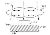
図4(A)は、ライン特徴105を有する半導体ウェハ100の平面図である。Z軸のライン特徴のアスペクトを測定するために、一般に、(X軸に沿って)特徴105とウェハ表面から断面スライスが切り取られて、特徴のX−Z諸特性を測定するための断面を得る。典型的には、集束イオンビーム(FIB)が用いられて、スライスされた断面を切り取る。そして、通常、SEMが用いられて、特徴断面のX−Z諸特性を測定する。実際、半導体製造業界においてはFIBとSEMの双方を有するデュアルビームシステムが通常使用され、単独の機器でこれらの機能をより有効に行う。しかし、当該業界において周知であるように、FIBは断面スライスを効果的に切り取ることに優れているが、一方、FIBは、一般的に言って、さほどクリーンではなく、測定されるべき特徴のアスペクトを有する周囲の領域の少なくとも一部を損傷することなしには、スライスを切り出すことができない。従って、保護堆積層は、上記のように、断面切り出し以前に、ウェハ100と特徴105の表面上に堆積される。 FIG. 4A is a plan view of the
図4(B)に関して、保護層を堆積するためには、通常、FIBそれ自体が使用される。それが断面スライスを切り取るのに使用されているので、堆積層を堆積するためのターゲット表面に対して照射する位置にFIBは既に存在している。これを実行するために、FIBビーム103は、ターゲット表面の近傍で放散された適切な堆積ガス120の存在の下で、関連性のあるウェハと特徴表面を有するターゲット表面に亘って走査され、ターゲット表面内の特徴とウェハの両表面上に保護材料を堆積する。ターゲット表面に衝突したとき、FIBビームがターゲット表面のビームが衝突した箇所からあらゆる方向に2次電子e-を放出させる。この電子は、ガスと互いに影響しあって微粒子を形成してその下の表面上に堆積する。図4(C)に示すように、方法が完遂したときに、堆積した微粒子で構成される保護層125は、ターゲット表面に亘ってできあがる。With reference to FIG. 4B, FIB itself is typically used to deposit the protective layer. Since it is used to cut cross-sectional slices, theFIB already exists at a position that irradiates the target surface for depositing the deposition layer. Toaccomplish this, the
残念なことに、FIBが最初にターゲット表面上で走査されるときに、十分な量の堆積材料が溜まってFIBから被照射特徴表面をシールドするまでの期間中表面から材料がスパッタされる。たとえこの時間は短いときでも、相当量の材料を取り除くことを可能にするほど十分長い場合もあり、このことは断面解析の精度を損なう原因となる。たとえば、図4(C)に示すように、ライン特徴105はその頂外縁をかなり丸くするものであるが、このことは、FIBに対する最大の非シールド露呈を招来する。このことは、特に、今日のチップ製造方法に使用される次第により小さな寸法で且つより小さな許容誤差にするときに問題となる。たとえば、丸く描かれたライン特徴に関して、その幅は、不正確に、ライン特徴が許容誤差外であると誤って評価されるほど小さく計測される。 Unfortunately, when the FIB is initially scanned over the target surface, material is sputtered from the surface for a period of time until a sufficient amount of deposited material has accumulated to shield the irradiated feature surface from the FIB. Even if this time is short, it may be long enough to allow a significant amount of material to be removed, which causes the accuracy of the cross-sectional analysis to be compromised. For example, as shown in FIG. 4C, the
上記のように、電子ビーム及びレザービームは、材料堆積のために必要な電子を発生するために使用される。しかし、それらは下地面を損傷することもあり得る。特に、それらが有望なスループットを達成するために十分なエネルギー及び/又は電流密度レベルにあるときには、損傷することもあり得る。しかし、下地面を傷付けないほど十分弱い場合には電子ビーム及びレザービームが一般的にあまりにも緩慢であるために、それらを用いることは通常実用的でない。更に、たとえば、デュアルビームシステムのような多くの環境の下で、それらはガス堆積用の適切なアングルでターゲット表面を走査するために正確に調整されるものではない。プラズマ蒸着(PVD)スパッタ方法は、いくつかの用途に使用可能であるかも知れないが、しかし、通常FIB製造制御用途に利用されることはない。何故ならば、それらがウェハ表面のターゲット部分に堆積層をローカルに塗布するためには使用できないからである。 As mentioned above, electron beams and razor beams are used to generate the electrons necessary for material deposition. However, they can damage the underlying surface. In particular, they can be damaged when they are at sufficient energy and / or current density levels to achieve a promising throughput. However, if they are weak enough that they do not damage the underlying surface, it is usually not practical to use them because the electron and razor beams are generally too slow. Furthermore, under many circumstances, for example, dual beam systems, they are not precisely adjusted to scan the target surface at the proper angle for gas deposition. The plasma deposition (PVD) sputtering method may be usable for some applications, but is not normally used for FIB production control applications. This is because they cannot be used to apply the deposited layer locally to the target portion of the wafer surface.
本発明の課題は、ターゲット面を実質的に傷付けることのないようにして材料を堆積する方法とシステムを提供することである。 It is an object of the present invention to provide a method and system for depositing material in a manner that does not substantially damage the target surface.
上記の課題を解決するため、本発明は、請求項1に記載したような「ワークピース上に材料を堆積する方法であって、該ワークピース上に、対象となる領域を囲繞するターゲット面を特定する工程と、前記ターゲット面に近接するも実質的に異なる電子源表面を限定する工程と、前記ターゲット面上に堆積ガスを提供する工程と、前記電子源表面の少なくとも一部に照射して、前記ターゲット面上の領域に突入する2次電子を発生する工程であって、該2次電子が前記堆積ガスと相互に影響しあって、前記対象領域を含む前記ターゲット面上に堆積材料の層を堆積し、前記ターゲット面内の前記対象領域が前記照射によっても損傷を受けないようにするものとからなる方法」を提供するものである。In order to solve the above problems, the present invention provides a method for depositing a material on a workpiece as described in claim 1, wherein a target surface surrounding a target region is formed on the workpiece. Illuminating at least a portion of the surface of the electron source, identifying a substantially different electron source surface inproximity to the target surface, providing a deposition gas on the target surface, , Generating secondary electrons that enter a region on the target surface, the secondary electrons interacting with the deposition gas, and the deposition material is deposited on the target surface including the target region. depositing a layer, in which the region of interest in the target surface to provide a method "consisting asto prevent even damaged by the irradiation.
また、第2の解決手段は、請求項8に記載したように、「ワークピース表面上に材料を堆積する方法であって、該ワークピース表面上においてターゲット面を特定する工程と、前記ターゲット面に近接する補助電子源表面を提供する工程と、前記ターゲット面上に堆積ガスを提供する工程と、前記補助電子源表面の少なくとも一部に照射して、前記ターゲット面上に放出する2次電子を発生し、該2次電子が前記堆積ガスと相互に影響しあって、前記ターゲット面上に堆積層を堆積する工程とからなる方法」であることを特徴とするものである。Further, the second solving means described in claim 8 is a method of depositing a material on a workpiece surface, the step of identifying a target surface on the workpiece surface, and the target surface. Providing an auxiliary electron source surfaceproximate to the target surface, providing a deposition gas on the target surface, and irradiating at least a part of the auxiliary electron source surface to emit secondary electrons on the target surface And the secondary electrons interact with the deposition gas to deposit a deposition layer on the target surface.
更に、第3の解決手段は、請求項16に記載したような、「ターゲット面を有する上面を具備するワークピースを収容するステージと、 ビームを前記ワークピースの上面に制御可能に放出するように構成されたカラムであって、前記ビームが前記上面に衝突するときに、2次電子を放出させるものと、前記ターゲット面に堆積ガスを提供するガス源と、前記カラムと連結して前記ビームを制御する制御器であって、前記ビームをワークピースの上面に導くものと、前記制御器によって実行されたときに、前記ターゲット面に近接するも前記ターゲット面の一部ではない電子源表面上において前記制御器がビームを走査する命令を前記制御器に提供して、前記ターゲット面上の前記電子源表面から2次電子を発生し、それが堆積ガスと共に相互反応し、それによって、前記ビームがターゲット面に入射することなく、堆積層を前記ターゲット面上に堆積させる記憶デバイスとからなるシステム」であることを特徴とするものである。Furthermore, the third solution is as set forth in claim 16, wherein a stage containing a workpiece having a top surface with a target surface and a beam controllably emitted onto the top surface of the workpiece. A column configured to emit secondary electrons when the beam collides with the upper surface; a gas source for providing a deposition gas to the target surface; and the column connected to the column. a controller for controlling, asguiding the beam on the upper surface of the workpiece, when executed by the controller, alsoadjacent to the target surface on not part surface of the electron source of the target surface The controller provides instructions to the beam to scan the controller to generate secondary electrons from the electron source surface on the target surface, which interact with the deposition gas. A system comprising a storage device that reacts and thereby deposits a deposition layer on the target surface without the beam being incident on the target surface.
本発明は、荷電粒子(たとえば、イオンや電子)又は光ビームを用いて、2次電子を発生してガス堆積材料内に堆積を誘発する、実質的に損傷のない材料堆積を行う方法を提供するものである。また、本発明は、ビームをターゲット表面に近接する電子源表面(ターゲット表面内ではない)に向けて照射する。このビームはその電子源表面上を走査されて2次電子をこの電子源表面から放出させ、ターゲット表面上の領域に突入させて堆積ガスと互いに影響しあって所望の量の材料をターゲット表面に堆積する。それとは別に、ビームはターゲット表面に近接する個々の電子発生面(好ましくは比較的に高い2次電子放出係数を有するもの)に向かって照射されて電子を発生し、ターゲット表面上に堆積材料を堆積する。The present invention provides a method for performing substantially undamaged material deposition using charged particles (eg, ions or electrons) or a light beam to generate secondary electrons to induce deposition within a gas deposition material. To do. The present invention also irradiates the beam toward the electron source surface (not within the target surface)close to the target surface. The beam is scanned over the surface of the electron source to cause secondary electrons to be emitted from the surface of the electron source and enter a region on the target surface to interact with the deposition gas and cause a desired amount of material to reach the target surface. accumulate. Alternatively, the beam is directed toward individual electron generating surfaces (preferably those having a relatively high secondary electron emission coefficient) close to the target surface to generate electrons, and deposit material on the target surface. accumulate.
上記の説明は、以下の発明の詳細な説明をよりよく理解することができるようにするために、本発明の特徴と技術的な利点をむしろ広範に略述したものである。別の本発明の特徴と技術的な利点は、以下に説明される。本発明と同じ目的を実行する他の構造物を改作又は設計するための基になるものとして、開示された概念と特別の実施の形態が容易に利用されうることは業界で通常の知識を有する者にとって明らかである。そのような均等な構造物が本明細書に添付の特許請求の範囲に記載された本発明の精神と範囲から逸脱するものではないことも、業界で通常の知識を有する者によって理解される。 The foregoing has outlined rather broadly the features and technical advantages of the present invention in order that the detailed description of the invention that follows may be better understood. Other inventive features and technical advantages are described below. It is common knowledge in the industry that the disclosed concepts and special embodiments can be readily utilized as a basis for adapting or designing other structures that perform the same purposes as the present invention. It is clear to the person. It will also be appreciated by those skilled in the art that such equivalent constructions do not depart from the spirit and scope of the invention as set forth in the claims appended hereto.
上記第1乃至第3の課題解決手段によれば、満足のいくスループットを有して、半導体特徴を明確には変更せずに半導体特徴上に保護層を堆積し、それによって、正確な計測のために半導体特徴を保存することができる効果を奏する。また、材料堆積を行うために使用されるビームにターゲット表面自体が照射されることなく、材料が適切な高速でターゲット表面上に堆積される効果も奏する。 According to the first to third problem solving means, a protective layer is deposited on a semiconductor feature with satisfactory throughput without clearly changing the semiconductor feature, thereby enabling accurate measurement. Therefore, the semiconductor characteristics can be preserved. In addition, there is an effect that the material is deposited on the target surface at an appropriate high speed without irradiating the target surface itself with the beam used for material deposition.
図1は、本発明の近接堆積方法の各種の実施の形態を実施するために最適なFIBシステムの一例を示す略図である。特定された構成要素は必ずしも全ての用途にとって必要なものではない。その上、図示されたサイズと相対的な位置は、必ずしも全ての構成にとって拡大縮小したり、一致する必要はない。 FIG. 1 is a schematic diagram showing an example of an optimal FIB system for carrying out various embodiments of the proximity deposition method of the present invention. The identified components are not necessary for all applications. In addition, the size and relative position shown do not necessarily have to be scaled or matched for all configurations.
図示されたFIBシステムは、イオンビーム217を発生してそれをイオンビーム集束カラム216に送る液体金属イオン(たとえば、ガリウムイオン)源214を有する真空チャンバ210を具備する。集束カラム216は、静電レンズや各電極(操作電極や偏向電極など)を有する従来の光学系と所望の集束イオンビーム218を生成してそれをターゲットのワークピース222に集束させることを可能にする他の構成部材を内蔵する。集束イオンビームと共に使用されるレンズと他の光学部材が静電界又は電磁界を利用してビーム内のイオンを制御することと、光学部材がイオン流を制御することを業界において通常の知識を有する者は理解する。更に、たった一つのレンズでも、又は数個までのレンズでも設計上可能である。The illustrated FIB system comprises a
イオンビーム217は、イオン源214から集束カラム216を通過して集束イオンビーム218となりワークピース222上の所望のポイントに向かう。ワークピース222は、真空チャンバ226の下部において移動X−Yステージ上に着脱自在に取り付けられている。ワークピース222は、集束イオンビーム218によって加工されて所望の結果を達成することができるいかなる材料でもよい。たとえば、半導体デバイスやホトリソグラフマスクや磁性ヘッドなどが含まれる。使用される特定タイプのビーム(たとえば、形状のあるなし、サイズ、ガリウムなどの素材)は、対象物質と希望する結果に依存する。たとえば、大電流によって厳密に集束された非拡大ビームが望ましいこともあるし、それとは別に、好適な電流密度プロファイルを有する集束以下の形状のあるビーム(又はそれに関して他の形状のビーム)が最適であるかも知れない。 The
イオンポンプ228が、ネック部210を排気するために用いられている。下部チャンバ226は、真空コントローラの制御の下でターボ分子メカニカルポンプシステム230によって排気される。高圧電源234は液体金属源214と集束カラム内の適切な電極に接続されており、適切な荷電イオンビーム218(たとえば、5KeV乃至30KeV)を形成してそれを下側に向ける。ビームコントローラ236は集束ビーム218を制御するために集束カラム216に接続され、所望の堆積タスクに関連して、ターゲットのワークピース222上で該ビームを走査し、回転し、変形し、及び/又は移動する。コントローラ236によって、利用者は、(図示しない)従来のユーザーインタフェースに入ったコマンドによって所望の方法で操作されるべきビーム218を制御することができる。それとは別に、ビームコントローラ236は、記憶デバイスにアクセスして命令をダウンロードし、該コントローラがシステムを制御して、損傷の原因となるイオンビーム218に露呈することがないように、ワークピースの所望の領域上に材料を堆積するための通路を走査するようにすることもできる。 An
液体金属イオン源214は、マルチカスプ又は他のプラズマイオン源のような他のイオン源も使用できるけれども、大抵はガリウムの金属イオンビームを提供するものである。液体ガリウム源は、大抵ワークピース222において1/10ミクロン以下の幅を有するビームに集束することができる。撮像用の2次放出を検出するために使用される電子倍増器240は、撮像電源及びコントローラ245とビデオ回路242に接続されている。ビデオ回路242はドライブ信号をビデオモニタ244に供給して、加工されている最中のワークピース222を表示する。 The liquid
ガス蒸気源246は、蛇腹252内の支持構造物を介してガス源を適切な位置に置くようにする変換デバイス248によってチャンバ226の側部の内側に配設されている。ガス蒸気源246は、ヒーター付きのタンク254を有し、そのタンクはメンブレンタイプの加熱器を有することもでき、タンク254内の化合物の温度を、ビーム誘導反応のために適切な分子流259を提供してワークピース222上に堆積される微粒子材料を形成する温度に上昇するのに使用される。注射針によって提供される毛細管からなる移送管又はノズル256は、タンク254から制御バルブ258を通ってノズル端257に延在して、図示のように円筒形状のノズル端257を通過するイオンビーム218に近接するワークピース222に向けてガス蒸気259を流す。制御バルブ258は、システムが制御自在にガス蒸気を放出することを可能にする。 The
タンク254は化合物をガス蒸気259に気化する所望の温度に上昇したとき、装置外からアクチュエータロッドを引っ張ってバルブプランジャの位置を開放調整してバルブ258が開放されるが、一方、円筒形状のノズル端257は、ワークピース222の所望の領域に向かって配向する。蛇腹252は、試料に対するノズル組み立て体とタンクの動きを吸収してチャンバ226内の真空度に影響を与えないようにする。化合物のガス蒸気259は、使用するワークピースとイオン源(又は他のビームタイプ)に関連して既定の目的に合致するような何れかの適切な堆積ガスであればよい。一つの実施の形態において、ガリウム源が使用されている場合、ヘキサカルボニルタングステン(W(CO)6)を有するガスが使用される。このガスがターゲットのワークピース222上で電子と相互に影響しあったとき、主にタングステンによって構成されるがガリウムも含んでいる堆積微粒子が構成され、従来のシリコンベースの半導体材料を保護するためによく機能する。When the temperature of the
ドア260は、ワークピース222を挿入してそれを加熱可能なステージ224上に載置するため、そして、タンク254を点検するために開扉する。ドア260は、タンク254内の温度が実質的に室温よりも上である場合には、開扉しないように連動されている。
真空制御システムは、ガス蒸気源246のヒーターと共に操作されて、材料堆積のためにワークピース222に向かうようにチャンバ内でガス蒸気フラックスを確立するための適切な蒸気圧条件を提供する。所定のガス蒸気フラックスを確立するために、タンク254が予め決められた温度に加熱される。 The vacuum control system is operated in conjunction with the heater of the
高圧電源234は、イオンビームカラム216内の電極に適切な加速電圧を印加してイオンビーム218を活発にし集束させる。ビームが濃縮されたガス蒸気が付着したワークピースに当たったときに、イオンビームはガス状の化合物と基板の間でワークピース上の材料堆積のための反応を引き起こすためのエネルギーを提供する。The high
前記のように、真空システムは、チャンバ226内に約1x10⁻⁷Torrと5x10⁻⁴Torrの間の真空を提供する。ガス蒸気の排気と共に、チャンバのバックグランド圧力(background pressure)は好適には約1x10⁻⁵Torrである。例示された実施の形態において、ガス蒸気源246は、注射針の毛細管を介して適切なガスフラックスを提供する温度に加熱されるが、一方、金属イオン源と集束カラムは適切に制御されて対応する好適なイオンフラックスを発生する。当該業界において通常の知識を有する者は、いずれの特定の用途においても好適な圧力とガス流を簡単に決定する。As described above, the vacuum system provides a vacuum between about 1 × 10⁻⁷ Torr and 5 × 10⁻⁴ Torr in
近接堆積
本発明の一の実施の形態において、相当高いエネルギー及び/又は相当大きな電流密度を有する荷電粒子(たとえばイオンや電子)又は光ビームを用いて、ターゲット面に直接照射することなく、電子源表面から2次電子を発生し該電子源表面に隣接するそのターゲット面上に蒸着を誘発することによって、ターゲット面上に実質的に傷のない材料堆積を行うことができる。この方法に関して、2次電子の適切なオーバーフローを発生するために、相当高いエネルギー、電流、及び/又は電流密度を有するいかなる粒子ビーム又は光ビームが使用される。このようなビームには、ターゲット面を避けて電子源表面に向かって放射され2次電子を発生する電子ビーム、イオン(たとえば、FIB)ビームやレザービームが含まれるが、これらに限定されるものではない。この方法を説明するために単純化して、FIBビームがここでは用いられるが、当該業界において通常の知識を有する者は他のビームも使用できることを理解する(たとえば、特に電子ビームが相当なエネルギーと電流を有するときには、電子ビームは2次電子を発生するためによく機能する。一つの実施の形態において、300eVと3KeVの間のエネルギーと1nAを超える電流値を有する電子ビームが使用されて半導体上に材料を堆積する)。Proximity Deposition In one embodiment of the present invention, an electron source is used without directly irradiating the target surface with a charged particle (eg, ion or electron) or light beam having a fairly high energy and / or a substantial current density By generating secondary electrons from the surface and inducing deposition on the target surface adjacent to the electron source surface, a substantially flawless material deposition can be performed on the target surface.Regarding this method, in order to generate a proper overflow of secondary electrons, much higher energy, current, and / or any particle beam or light beam having a current density is used. Such beams include, but are not limited to, electron beams that are emitted toward the surface of the electron source away from the target surface to generate secondary electrons, ion (eg, FIB) beams, and laser beams. is not. In order to simplify this method, FIB beams are used here, but those having ordinary knowledge in the industry will understand that other beams can be used (for example, electron beams in particular have significant energy and When having a current, the electron beam functions well to generate secondary electrons, hi one embodiment, an electron beam having an energy between 300 eV and 3 KeV and a current value greater than 1 nA is used on the semiconductor. To deposit material).
ターゲット面は、まず、材料堆積層を受けるために限定される。ターゲット面は、一般的に、ウェハ基板表面を囲繞すると共に、(たとえば、計測又は解析のための)対象となる一又はそれ以上の特徴の少なくとも一部を含む。ターゲット面は、一又はそれ以上の特徴の重要な部分がFIBによって適切に衝撃を受けないようにする程十分に広くなくてならない。同時に、2次電子が十分な材料堆積を誘起するために適切にターゲット面の領域に浸透することができるほどに狭いものである(及び/又は適切な幾何学形状を有している)べきである。The target surface is first limited to receive the material deposition layer. The target surface generally surrounds the wafer substrate surface andincludes at least a portion of one or more features of interest (eg, for metrology or analysis). The target surface must be wide enough so that a critical portion of one or more features is not properly impacted by the FIB. At the same time, it should be narrow enough (and / or have a suitable geometry) that secondary electrons can adequately penetrate the area of the target surface to induce sufficient material deposition. is there.
一度ターゲット面が特定されると、電子源表面が2次電子を提供するために限定される。電子源表面の領域は、通常ターゲット面に隣接している。それは電子源表面の領域にオーバーフローするほどの満足のできる量の2次電子を作り出す程十分広いか又は適切な形状を有すべきである。一般的に、ターゲット面の周囲で実質的に均一な形状に電子源表面の領域を限定して、2次電子がより均等にターゲット面の領域に分配されるようにすることが望ましく、それによって、結果的により均一な材料堆積層となる。(しかし、ビーム衝突点からの距離が遠くなるにつれて2次電子の濃度が薄くなり、所定のポイントでの材料堆積量がそのポイントにおける利用可能な電子の濃度に比例するので、現実的な均一性を達成することは難しい。このように、電子源表面のビーム衝突点から最大の平均距離を有するターゲット面内の各ポイントは、より薄い材料堆積となる。)多くの場合、ターゲット面を囲繞する閉じた電子源表面を有することが望ましいが、しかし、それらはあらゆる場合にターゲット面を囲繞する必要もない。更に、電子源表面は、矩形や長円形や三角形のようないかなる適切な形状を有することも可能である。Once the target surface is identified, the electron source surface is limited to provide secondary electrons. The region of the electron source surface is usually adjacent to the target surface.It should be wide enough or have a suitable shape to produce a sufficient amount of secondary electrons to overflow into the areaof the electron source surface. In general, it is desirable to limit the area of the electron source surface to a substantially uniform shape around the target surface so that secondary electrons are more evenly distributed to the area of the target surface, thereby This results in a more uniform material deposition layer. (However, as the distance from the beam collision point increases, the concentration of secondary electrons decreases, and the amount of material deposited at a given point is proportional to the concentration of available electrons at that point, so that there is realistic uniformity. Thus, each point in the target surface that has the greatest average distance from the beam impact point on the electron source surface results in a thinner material deposition.) In many cases, surrounds the target surface It is desirable to have a closed electron source surface, but they do not need to surround the target surface in any case. Furthermore, the electron source surface can have any suitable shape, such as a rectangle, oval, or triangle.
最後に、蒸着ガスが供給されてターゲット面の領域内で放散され、同時に、FIBビームが電子源表面を走査してターゲット表面領域のための2次電子を発生する。いくつかのライン特徴を有する半導体ウェハを用いた一つの例を以下に説明する。 Finally, the deposition gas is supplied and dissipated in the area of the target surface, and at the same time, the FIB beam scans the electron source surface to generate secondary electrons for the target surface area. One example using a semiconductor wafer having several line features is described below.
図2(A)乃至図2(D)は、本発明の一実施の形態に関連して材料堆積の各段階におけるウェハ300を示しているが、該ウェハ300はライン特徴305A−305Eを有している。これらのライン特徴は、ウェハ300のダイのうちの一つにおいて密集した配設されたライン導体の領域内に存在する。この実施の形態において、内側の3つのライン特徴305B、305C、305Dが計測されるべきものである。(最初と5番目のライン特徴305Aと305Eは、緩衝領域としてターゲット領域に入っており、対象特徴305B−305Dがより確実にイオンのオーバーショットから保護されることとなる。)多くの品質制御手法に応じてチップ製造工程中にライン特徴のうちの代表的な試料の深さと内側の幅を計測することが望ましい。本発明の一つの利点は、デュアルビームシステムでFIBを使用して保護材料を堆積すること並びに解析のために断面を切り出すことができることによって、測定がFIBによって、希望する場合には、製造ライン上で正しく効率的に行われる。更に、ターゲット材料堆積ができないPVD方法とは異なり、FIB堆積方法に関して、測定工程においてウェハ上で破壊されねばならないのは、単独のダイのみである。このように、残りのチップダイに関しては、ウェハは以後の工程や商品化のためにラインをたどることができる。 2A-2D illustrate a
図2(A)及び図2(B)に関して、ウェハ表面は、四角形の枠状の電子源表面315によって囲繞された四角形状のターゲット面310を有する。正確な縮尺で表示されてはいないが、各ライン特徴305A−305Eの(Y軸上の)幅は約0.2μmであり、それらの間の空間も約0.2μmである。従って、図示されたターゲット面310の幅は、約2.0μmである。図2(B)は、ウェハ300の断面を示している。それは、FIBビーム303が電子源表面315の左部分の一点に向けて照射されていることを示している。図示のように、2次電子e-がビーム衝突点から四方八方に放出している。2A and 2B, the wafer surface has a
この実施の形態においては、中央の3本のライン特徴(305B、305C、305D)のみが測定される。しかし、特定のターゲット面が限定されて5本のラインを囲繞するが、これは一方で、堆積中のターゲット面へのFIBイオンの過度の放射から適切に測定すべき内側の3本のラインを保護することと、他方で、ターゲット面の全幅を最小にして2次電子がターゲット面内の全ての点に容易にたどり着くことができるようにすることとの妥協の結果である。In this embodiment, only the central three line features (305B, 305C, 305D) are measured. However, the specific target surface is limitedand surrounds five lines, which on the other hand is the inner three lines that should be properly measured from excessive emission of FIB ions to the target surface being deposited. and it is protected, on the other hand,is the result of compromise between the secondary electrons and the full width of the target surface to a minimum to be able to reach easily to all points in the target plane.
図2(C)は、その上に材料が堆積されているときのウェハの平面図である。それは、供給された堆積ガスが全体領域に放散されていると共に、2次電子e-が放出されていることを示している。図示のように、2次電子e-は電子源表面315の至る所から四方八方に放出している。しかし、それらは電子源表面315のあらゆる点から同時に放出されるものではない。むしろ、それらは、FIBビーム303によって衝撃を加えられたその時点で衝撃点から放出される。ターゲット面310内における電子の比較的均一な配分を維持するためには電子源表面315の至る所で高速でFIBビームが走査されるべきだからである。高速走査のために、ビームは、高速で点から点に移動され(即ち、停止時間が短くされビームが点から点に迅速に移動される)か、若しくは、インタレースタイプの走査パターンが使用され、それによって、電子源表面に亘って均一に散らばっている異なる点が走査フレーム毎にスキップされる。勿論、これら手法のいかなる組み合わせも使用することが可能である。FIG. 2C is a plan view of the wafer as material is deposited thereon. It shows that the supplied deposition gas is diffused to the whole area and secondary electrons e− are emitted. As shown in the figure, secondary electrons e− are emitted from all over the
別の用例においては、異なるサイズの電子源表面とターゲット面が同様に使用される。それに応じて、処理対象物に依存して、別々の場合において異なるビームパラメータが使用される。一つの実施の形態において、点から点の入射ビームの停止時間は、異なるサイズのビーム電流、電流密度、ビームスポット直径が使用されていても、一定である。特定のビームパラメータを選択したときに、いくつかの要因が考慮される。ビームスポットのサイズは、通常、電子源表面のサイズと面積に依存して決定される。電子源表面領域が広い場合には、ターゲット面に衝突しないで、電子源表面の領域に最も余裕のない状態でビームスポットが適切にはまりこむ限り、より大きなビームスポット領域であることが望ましい。しかし、ビーム電流と電流密度は、ターゲット面のサイズと面積に応じて選択されるべきであり、同様に、電子源表面の材料の2次電子放出特性に応じて選択されるべきである。より大きな電流密度は、一般的に、電子をより遠くに放出しより濃い濃度にする。このように、ターゲット面が電子源表面の最も近いビーム衝撃点からも比較的に遠い内部部分を有しているので、より大きな電流密度を有するビームが使用されるべきである。一方、電流密度があまりにも大きすぎると、余分な材料が電子源表面から跳ね返って2次電子のターゲット面への移動に悪影響を及ぼす。ウェハ表面における真空度が、また、2次電子がどの程度速く移動するのかについて影響する。一つの実施の態様においては、12.5nmのスポット直径を有する30μAのビームが小さなターゲット面に使用され、一方、25μmのスポット直径を有する300nAのビームがより大きなターゲット面に使用されている。Inanother example, the electron source surface and the target surface of different sizesare used as well. Accordingly, different beam parameters are used in different cases depending on the object to be processed. In one embodiment, the point-to-point incident beam stop time is constant even when different sizes of beam current, current density, and beam spot diameter are used. Several factors are considered when selecting specific beam parameters. The size of the beam spot is usually determined depending on the size and area of the electron source surface. When the electron source surface area is large, it is desirable that the beam spot area is larger as long as the beam spot is appropriately fitted without colliding with the target surface and with the least margin in the area of the electron source surface. However, the beam current and current density should be selected according to the size and area of the target surface, and similarly according to the secondary electron emission characteristics of the material on the electron source surface. A larger current density generally emits electrons farther to a higher concentration. Thus, since the target surface has an internal portion that is relatively far from the nearest beam impact point of the electron source surface, a beam with a higher current density should be used. On the other hand, if the current density is too large, excess material will bounce off the electron source surface and adversely affect the movement of secondary electrons to the target surface. The degree of vacuum at the wafer surface also affects how fast secondary electrons move. In one embodiment, a 30 μA beam with a 12.5 nm spot diameter is used for the small target surface, while a 300 nA beam with a 25 μm spot diameter is used for the larger target surface.
最後に、図2(D)は、材料325が電子源表面315上に堆積された後のウェハ300の断面を示している。図示のように、材料325は電子源表面上で最も厚く、そこで2次電子密度が最も大きくなる。材料の厚みをみると、電子源表面から遠くへの2次電子の移動を少なくさせたことが予想される。材料は、また、ターゲット面から離れた電子源表面の外側にも堆積する。何故ならば、電子と堆積ガスが存在するときにはいつでも材料は堆積されるからである。このように、ウェハの決められた領域に材料を堆積しないようにしたいときには、ガスがその決められた領域に放散されないような手段若しくは2次電子がそれに至らないようにする手段のいずれかが執られるべきである。 Finally, FIG. 2D shows a cross section of the
他の実施の形態
図3は、ターゲット面に2次電子を供給する別の方式を図示している。図示されたFIBビーム403をウェハのターゲット面310に近接する電子源表面に向けて照射する代わりに、図示の場合には、堆積ガス459をウェハに向けて放出するために使用されるノズル端ピース457の内部金属面である補助電子源表面に向けて照射するものである。この補助電子源表面は、ターゲット面と共通の面を有さない面であり2次電子をそのターゲット面に提供するものであればよい。たとえば、入射ビームによる衝撃に応じて2次電子を提供するために、(ガスがそこに供給され続ける)ターゲット面に調節自在に近接配置されたプレートや型やツールである。FIBに関しては、電子ビームやレザーや高2次電子放出係数を有する金属のような材料が一般的に望ましいが、しかし、いかなる入手可能な好適な材料でも十分である。ターゲット面に既に近接している(ガスノズル端のような)構造物を使用することはより便利である。
Other Embodiments FIG. 3 illustrates another method for supplying secondary electrons to the target surface. Instead of irradiating the illustrated
2次電子をターゲット面に向ける配向機器も利用できる。たとえば、静電界及び/又は電磁界発生機器が使用されうる。静電界及び電磁界は、ターゲット面の周囲の軌道で入射ビームを動かすためには、静的なものであってもよいし動的なものであってもよい。静電界に関して、ワークピース自体が一又はそれ以上の個々の操作電極と組み合わせて使用されるか、それとは別に、もっぱら個々の電極がその静電界を確立するために使用される。一つの実施の態様においては、一又はそれ以上の個々の電極が、2次電子をターゲット面に対して内側に向けるために、ターゲット面を囲繞する静電界(電磁界)を生成するために構成されている。 An orientation device that directs secondary electrons to the target surface can also be used. For example, an electrostatic field and / or electromagnetic field generator can be used. The electrostatic and electromagnetic fields may be static or dynamic in order to move the incident beam in a trajectory around the target surface. With respect to the electrostatic field, the workpiece itself is used in combination with one or more individual operating electrodes, or alternatively, only individual electrodes are used to establish the electrostatic field. In one embodiment, one or more individual electrodes are configured to generate an electrostatic field (electromagnetic field) that surrounds the target surface to direct secondary electrons inward relative to the target surface. Has been.
上記のように本発明とその利点が詳細に説明されてきたが、各種の変形と代替と変更が、特許請求の範囲に記載された発明の精神とその範囲を逸脱しないで、なされうることを理解されるべきである。更に、本出願の範囲は、この明細書に記載されたプロセスと機械と製造物と組成物と方法と工程の特定の実施の形態に制限されることを意図するものではない。当該業界で通常の知識を有する者は本発明の開示事項から容易に正当に認識する限り、現に存在しているか又はこれから開発されてここに説明された対応する実施の形態と実質的に同じ機能を行い又は実質的に同じ結果を達成するであろうプロセスと機械と製造物と組成物と手段と方法と工程を構成要素と工程が本発明に従って利用される。従って、特許請求の範囲の記載は、そのようなプロセスと機械と製造物と組成物と手段と方法と工程をその範囲内に有することを意図するものである。 Although the invention and its advantages have been described in detail as described above, it will be understood that various modifications, substitutions and changes may be made without departing from the spirit and scope of the invention as defined in the claims. Should be understood. Furthermore, the scope of the present application is not intended to be limited to the specific embodiments of the processes, machines, products, compositions, methods, and steps described herein. To those skilled in the art, as long as it is readily and legitimately recognized from the disclosure of the present invention, functions that are presently present or developed in the future and substantially the same functions as the corresponding embodiments described herein. Components, steps, processes, machines, products, compositions, means, methods, and steps that will perform or achieve substantially the same results are utilized in accordance with the present invention. Accordingly, the appended claims are intended to include within their scope such processes, machines, manufacture, compositions of matter, means, methods, or steps.
上述したように、本発明の方法等は、半導体等に材料を堆積する場合に利用される。 As described above, the method of the present invention is used when a material is deposited on a semiconductor or the like.
210…ネック部、214…液体金属イオン源、216…イオンビーム集束カラム、217…イオンビーム、218…集束イオンビーム、222…ワークピース、224…X−Yステージ、226…下部チャンバ、228…イオンポンプ、230…ポンプシステム、232…真空コントローラ、234…高圧電源、240…電子倍増器、242…ビデオ回路、244…ビデオモニタ、245…撮像電源及びコントローラ、246…ガス蒸気源、248…変換デバイス、252…蛇腹、254…タンク、256…ノズル、257…ノズル端、258…制御バルブ、259…ガス蒸気、260…ドア、300…ウェハ、303,403…FIBビーム、305…ライン特徴、310…ターゲット面、315…電子源表面、320,459…堆積ガス、457…ノズル端ピース
210 ... Neck part, 214 ... Liquid metal ion source, 216 ... Ion beam focusing column, 217 ... Ion beam, 218 ... Focused ion beam, 222 ... Workpiece, 224 ... XY stage, 226 ... Lower chamber, 228 ... Ions Pump, 230 ... pump system, 232 ... vacuum controller, 234 ... high voltage power supply, 240 ... electron multiplier, 242 ... video circuit, 244 ... video monitor, 245 ... imaging power supply and controller, 246 ... gas vapor source, 248 ...
Claims (26)
Translated fromJapanese前記ワークピース上に、対象となる領域を囲繞するターゲット面を特定する工程と、
前記ワークピース上に、前記ターゲット面と異なる電子源表面を限定する工程と、
前記ターゲット面上に堆積ガスを提供する工程と、
前記荷電粒子ビームにより前記電子源表面を照射して、前記ターゲット面上の領域に突入する2次電子を発生する工程であって、該2次電子が前記堆積ガスと相互に影響しあって、前記対象領域を含む前記ターゲット面上に堆積材料の保護層を堆積し、該保護層を堆積している間は前記荷電粒子ビームが前記ターゲット面に衝突しないようにし、更に、前記ターゲット面内の前記対象領域が前記照射によって損傷を受けないようにするものと、
堆積材料の保護層の堆積後に、荷電粒子ビームを前記ターゲット面に向けて照射して前記ターゲット面を処理する工程とからなる方法。Providing a protective layer on the target surface of the workpiece by depositing material onthe target surface of the workpiecewithout directing a charged particle beam ontothe target surfacecomprising a part of the workpiece; A methodfor protecting the target surface during processing of a charged particle beam comprising :
Onthe workpiece, and specifying the target surface surrounding the region of interest,
On the workpiece, a step of defining said target surfacedifferent from the electron source surface,
Providing a deposition gas on the target surface;
Wherein byirradiating the electron source tablesurfaceby a charged particle beam, wherein a step of generating the secondary electrons enters the area on the target surface, said secondary electrons each other affect each other and said deposition gas Depositing aprotective layer of deposition material on the target surface including the target region,preventing the charged particle beam from colliding with the target surface while the protective layer is being deposited;to that the target areais to avoid damage by the irradiation,
A methodof treating the target surface by irradiating acharged particle beam toward the target surfaceafter the deposition of the protective layer of the deposition material .
該ワークピース表面上においてターゲット面を特定する工程と、
前記ターゲット面とは別に、前記ターゲット面領域にオバーフローする二次電子を生成するように形成された補助電子源表面を提供する工程と、
前記ターゲット面上に堆積ガスを提供する工程と、
前記荷電粒子ビームにより前記補助電子源表面を照射して、前記ターゲット面上に放出する2次電子を発生し、該2次電子が前記堆積ガスと相互に影響しあって、前記ターゲット面上に堆積材料の保護層を堆積する工程であって、該保護層を堆積している間は前記荷電粒子ビームが前記ターゲット面に衝突しないようにするものと、
堆積材料の保護層の堆積後に、荷電粒子ビームを前記ターゲット面に向けて照射して前記ターゲット面を処理するようにする工程とからなる方法。Providing a protective layer on the target surface of the workpiece by depositing material onthe target surfaceof the workpiece surfacewithout directing a charged particle beam ontothe target surfacecomprising a part of the workpiece; A method ofprotecting the target surface during processing of a charged particle beam of
Identifying a target surface on the workpiece surface;
A step of providing said toseparate from the target surface,the formed auxiliary electron source surfaceto generate secondary electrons overflow the target surface area,
Providing a deposition gas on the target surface;
Irradiating the surfaceof the auxiliary electron source with thecharged particle beam to generate secondary electrons to be emitted on the target surface, the secondary electrons interacting with the deposition gas, and on the target surface Depositinga protective layer of depositedmaterialto prevent the charged particle beam from colliding with the target surface during the deposition of the protective layer ;
Irradiating acharged particle beam toward the target surfaceafter the deposition of the protective layer of the deposition materialto treat the target surface .
対象となる領域を囲繞する前記ターゲット面を有する上面を具備するワークピースを収容するステージと、
前記荷電粒子ビームを前記ワークピースの上面に制御可能に放出するように構成されたカラムであって、前記ビームが前記上面に衝突するときに、2次電子を放出させるものと、
前記ターゲット面に堆積ガスを提供するガス源と、
前記カラムと連結して前記ビームを制御する制御器であって、前記ビームをワークピースの上面に導くものと、
前記制御器によって実行されたときに、前記制御器に行わせる命令を前記制御器に提供する記憶デバイスであって、前記命令は電子源表面上において前記ビームを走査して2次電子を発生させ前記ターゲット面上に前記電子源表面からの2次電子を送り、それが堆積ガスと共に相互反応し、それによって、前記ビームがターゲット面に入射することなく、堆積材料の保護層を前記ターゲット面上に堆積させ、そして、堆積材料の保護層の堆積後には、荷電粒子ビームを前記ターゲット面に向けて照射して前記ターゲット面を処理させるように制御器を命令するものである記憶デバイスとからなるシステム。Providing a protective layer on the target surface of the workpiece by depositing material on the target surface of the workpiece without directing a charged particle beam onto the target surface comprising a part of the workpiece; A system for protecting the target surface during processing of a charged particle beam,
A stage containing a workpiece comprising an upper surface having the target surfacesurrounding a region of interest ;
A column configured to controllably emit thecharged particle beam onto the upper surface of the workpiece, the column emitting secondary electrons when the beam collides with the upper surface;
A gas source for providing a deposition gas to the target surface;
A controller connected to the column to control the beam, which guides the beam to the upper surface of the workpiece;
A storage device that , when executed by thecontroller, provides instructions to the controller to cause the controller to scan the beam over the surfaceof the electron sourceto generate secondary electrons.feeding secondary electrons from the electron source surfaceonto the target surface, it is cross-reactive with the deposition gas, whereby said without beam is incident on the target surface, on the target surfaceprotective layerof the depositedmaterialAnda storage devicethat directs a controller to irradiate acharged particle beam toward the target surface to process the target surfaceafter deposition of a protective layer of deposited material. system.
を堆積させた後でFIBビームが前記特徴からスライスを切り取るようにする命令を前記
記憶デバイスが有していることを特徴とする請求項19に記載のシステム。The column is a FIB column that emits a FIB beam, and the storage device has instructions that cause the FIB beam to cut a slice from the feature after depositing a deposition layer on a target surface; 20. A system according to claim 19, characterized in that
に構成されたSEMを具備していることを特徴とする請求項20に記載のシステム。21. The system of claim 20, further comprising a SEM configured to image a cross section of the feature at a surface exposed by the cut slice.
一又はそれ以上の電極を具備することを特徴とする請求項16に記載のシステム。The system of claim 16, further comprising one or more electrodes configured to generate an electrostatic field that directs secondary electrons toward the target surface.
生することを特徴とする請求項22に記載のシステム。23. The system of claim 22, wherein the one or more electrodes generate an electrostatic field that causes a beam to travel around the target surface.
ングステン(W(CO)6)を有し、前記ビームがガリウムイオンを有することを特徴と
する請求項16に記載のシステム。The system of claim 16, wherein the workpiece is a silicon-based wafer, the deposition gas comprises hexacarbonyltungsten (W (CO) 6), and the beam comprises gallium ions.
Applications Claiming Priority (2)
| Application Number | Priority Date | Filing Date | Title |
|---|---|---|---|
| US10/607,814US6926935B2 (en) | 2003-06-27 | 2003-06-27 | Proximity deposition |
| US10/607,814 | 2003-06-27 |
Publications (3)
| Publication Number | Publication Date |
|---|---|
| JP2005015922A JP2005015922A (en) | 2005-01-20 |
| JP2005015922A5 JP2005015922A5 (en) | 2007-08-30 |
| JP4730875B2true JP4730875B2 (en) | 2011-07-20 |
Family
ID=33418722
Family Applications (1)
| Application Number | Title | Priority Date | Filing Date |
|---|---|---|---|
| JP2004188935AExpired - Fee RelatedJP4730875B2 (en) | 2003-06-27 | 2004-06-25 | Proximity deposition method and system |
Country Status (5)
| Country | Link |
|---|---|
| US (1) | US6926935B2 (en) |
| EP (1) | EP1491654B1 (en) |
| JP (1) | JP4730875B2 (en) |
| DE (1) | DE602004027446D1 (en) |
| TW (1) | TWI373791B (en) |
Families Citing this family (37)
| Publication number | Priority date | Publication date | Assignee | Title |
|---|---|---|---|---|
| US7495232B2 (en) | 2003-10-16 | 2009-02-24 | Alis Corporation | Ion sources, systems and methods |
| US7554097B2 (en) | 2003-10-16 | 2009-06-30 | Alis Corporation | Ion sources, systems and methods |
| US7485873B2 (en) | 2003-10-16 | 2009-02-03 | Alis Corporation | Ion sources, systems and methods |
| US7557361B2 (en) | 2003-10-16 | 2009-07-07 | Alis Corporation | Ion sources, systems and methods |
| US7557358B2 (en) | 2003-10-16 | 2009-07-07 | Alis Corporation | Ion sources, systems and methods |
| US7488952B2 (en) | 2003-10-16 | 2009-02-10 | Alis Corporation | Ion sources, systems and methods |
| US7554096B2 (en) | 2003-10-16 | 2009-06-30 | Alis Corporation | Ion sources, systems and methods |
| US7511279B2 (en) | 2003-10-16 | 2009-03-31 | Alis Corporation | Ion sources, systems and methods |
| US9159527B2 (en) | 2003-10-16 | 2015-10-13 | Carl Zeiss Microscopy, Llc | Systems and methods for a gas field ionization source |
| US7504639B2 (en) | 2003-10-16 | 2009-03-17 | Alis Corporation | Ion sources, systems and methods |
| US7521693B2 (en) | 2003-10-16 | 2009-04-21 | Alis Corporation | Ion sources, systems and methods |
| US7601953B2 (en) | 2006-03-20 | 2009-10-13 | Alis Corporation | Systems and methods for a gas field ion microscope |
| US7518122B2 (en) | 2003-10-16 | 2009-04-14 | Alis Corporation | Ion sources, systems and methods |
| US7557359B2 (en) | 2003-10-16 | 2009-07-07 | Alis Corporation | Ion sources, systems and methods |
| US8110814B2 (en) | 2003-10-16 | 2012-02-07 | Alis Corporation | Ion sources, systems and methods |
| US7557360B2 (en) | 2003-10-16 | 2009-07-07 | Alis Corporation | Ion sources, systems and methods |
| US7511280B2 (en) | 2003-10-16 | 2009-03-31 | Alis Corporation | Ion sources, systems and methods |
| US7786451B2 (en) | 2003-10-16 | 2010-08-31 | Alis Corporation | Ion sources, systems and methods |
| US7368727B2 (en) | 2003-10-16 | 2008-05-06 | Alis Technology Corporation | Atomic level ion source and method of manufacture and operation |
| US7786452B2 (en) | 2003-10-16 | 2010-08-31 | Alis Corporation | Ion sources, systems and methods |
| WO2007067296A2 (en)* | 2005-12-02 | 2007-06-14 | Alis Corporation | Ion sources, systems and methods |
| JP5600371B2 (en)* | 2006-02-15 | 2014-10-01 | エフ・イ−・アイ・カンパニー | Sputtering coating of protective layer for charged particle beam processing |
| JP2008171800A (en)* | 2006-10-31 | 2008-07-24 | Fei Co | Protective layer for charged particle beam processing |
| US8835880B2 (en)* | 2006-10-31 | 2014-09-16 | Fei Company | Charged particle-beam processing using a cluster source |
| US7804068B2 (en) | 2006-11-15 | 2010-09-28 | Alis Corporation | Determining dopant information |
| JP5695818B2 (en)* | 2009-01-27 | 2015-04-08 | 株式会社日立ハイテクサイエンス | Cross-section processing method and cross-section observation sample manufacturing method |
| US8987678B2 (en) | 2009-12-30 | 2015-03-24 | Fei Company | Encapsulation of electrodes in solid media |
| US8642974B2 (en) | 2009-12-30 | 2014-02-04 | Fei Company | Encapsulation of electrodes in solid media for use in conjunction with fluid high voltage isolation |
| EP2341525B1 (en) | 2009-12-30 | 2013-10-23 | FEI Company | Plasma source for charged particle beam system |
| EP2402475A1 (en)* | 2010-06-30 | 2012-01-04 | Fei Company | Beam-induced deposition at cryogenic temperatures |
| US20130098871A1 (en) | 2011-10-19 | 2013-04-25 | Fei Company | Internal Split Faraday Shield for an Inductively Coupled Plasma Source |
| EP2787523B1 (en)* | 2013-04-03 | 2016-02-10 | Fei Company | Low energy ion milling or deposition |
| DE102013012225A1 (en) | 2013-07-23 | 2015-01-29 | Carl Zeiss Microscopy Gmbh | Method for TEM lamella fabrication and assembly for TEM lamellae protection device |
| WO2015175934A1 (en)* | 2014-05-15 | 2015-11-19 | Anthony John Mark | Deposition and patterning using emitted electrons |
| EP3249676B1 (en) | 2016-05-27 | 2018-10-03 | FEI Company | Dual-beam charged-particle microscope with in situ deposition functionality |
| JP6900027B2 (en)* | 2017-03-28 | 2021-07-07 | 株式会社日立ハイテクサイエンス | Sample trench embedding method |
| US11817395B2 (en)* | 2020-09-29 | 2023-11-14 | Fei Company | Depositive shielding for fiducial protection from redeposition |
Family Cites Families (10)
| Publication number | Priority date | Publication date | Assignee | Title |
|---|---|---|---|---|
| JPS54124879A (en)* | 1978-03-22 | 1979-09-28 | Nippon Telegr & Teleph Corp <Ntt> | Ion beam deposition |
| JPH05159960A (en)* | 1991-12-09 | 1993-06-25 | Hitachi Ltd | Manufacture of magnetized film |
| US5429730A (en)* | 1992-11-02 | 1995-07-04 | Kabushiki Kaisha Toshiba | Method of repairing defect of structure |
| JP3132938B2 (en)* | 1993-02-03 | 2001-02-05 | セイコーインスツルメンツ株式会社 | Charged beam device for cross-section processing observation and processing method |
| JP3041174B2 (en)* | 1993-10-28 | 2000-05-15 | 株式会社東芝 | Pattern correction method in pattern correction device of electron beam lithography system |
| DE4340956C2 (en) | 1993-12-01 | 2002-08-22 | Advantest Corp | Method and device for processing a sample |
| JP4137317B2 (en) | 1999-10-07 | 2008-08-20 | 独立行政法人科学技術振興機構 | Micro three-dimensional structure, manufacturing method thereof, and manufacturing apparatus thereof |
| WO2001054163A1 (en) | 2000-01-21 | 2001-07-26 | Koninklijke Philips Electronics N.V. | Shaped and low density focused ion beams |
| US7326445B2 (en) | 2000-11-29 | 2008-02-05 | Sii Nanotechnology Inc. | Method and apparatus for manufacturing ultra fine three-dimensional structure |
| JP2004537758A (en) | 2001-07-27 | 2004-12-16 | エフ・イ−・アイ・カンパニー | Electron beam processing |
- 2003
- 2003-06-27USUS10/607,814patent/US6926935B2/ennot_activeExpired - Lifetime
- 2004
- 2004-04-23TWTW093111336Apatent/TWI373791B/ennot_activeIP Right Cessation
- 2004-06-21EPEP04076811Apatent/EP1491654B1/ennot_activeExpired - Lifetime
- 2004-06-21DEDE602004027446Tpatent/DE602004027446D1/ennot_activeExpired - Lifetime
- 2004-06-25JPJP2004188935Apatent/JP4730875B2/ennot_activeExpired - Fee Related
Also Published As
| Publication number | Publication date |
|---|---|
| US20040261719A1 (en) | 2004-12-30 |
| EP1491654A1 (en) | 2004-12-29 |
| TWI373791B (en) | 2012-10-01 |
| EP1491654B1 (en) | 2010-06-02 |
| DE602004027446D1 (en) | 2010-07-15 |
| TW200509219A (en) | 2005-03-01 |
| JP2005015922A (en) | 2005-01-20 |
| US6926935B2 (en) | 2005-08-09 |
Similar Documents
| Publication | Publication Date | Title |
|---|---|---|
| JP4730875B2 (en) | Proximity deposition method and system | |
| JP2005015922A5 (en) | ||
| US6949756B2 (en) | Shaped and low density focused ion beams | |
| TWI631343B (en) | Methods and devices for examining an electrically charged specimen surface | |
| JP6366216B2 (en) | Method for making thin samples for TEM imaging | |
| US7893397B2 (en) | Apparatus and method for surface modification using charged particle beams | |
| JP5779210B2 (en) | Charged particle beam inspection method and apparatus | |
| TWI873255B (en) | Filling empty structures with deposition under high-energy sem for uniform de layering | |
| EP2124244B1 (en) | Ultra high precision measurement tool with control loop | |
| US7256405B2 (en) | Sample repairing apparatus, a sample repairing method and a device manufacturing method using the same method | |
| US6297503B1 (en) | Method of detecting semiconductor defects | |
| JP7728486B2 (en) | Increasing deposition rate with a thermal insulating cover for GIS manipulators | |
| TW202433051A (en) | Method for creating a smooth diagonal surface using a focused ion beam and an innovative scanning strategy | |
| US12230473B2 (en) | Temperature-controlled surface with a cryo-nanomanipulator for improved deposition rate | |
| JP2025530409A (en) | Enhancement of deposition rate by applying negative voltage to gas injection nozzle in focused ion beam system | |
| US20050211896A1 (en) | Pt coating initiated by indirect electron beam for resist contact hole metrology | |
| JPH0680662B2 (en) | IC element correction method | |
| JP2025514718A (en) | Reduced charging due to low negative voltage in FIB system | |
| JP2025531601A (en) | Optimized saddle nozzle design for gas injection systems. | |
| JP2015132623A (en) | charged particle beam inspection method and apparatus | |
| JPH0680672B2 (en) | IC element processing equipment |
Legal Events
| Date | Code | Title | Description |
|---|---|---|---|
| RD04 | Notification of resignation of power of attorney | Free format text:JAPANESE INTERMEDIATE CODE: A7424 Effective date:20060609 | |
| A621 | Written request for application examination | Free format text:JAPANESE INTERMEDIATE CODE: A621 Effective date:20070619 | |
| A521 | Request for written amendment filed | Free format text:JAPANESE INTERMEDIATE CODE: A523 Effective date:20070713 | |
| A977 | Report on retrieval | Free format text:JAPANESE INTERMEDIATE CODE: A971007 Effective date:20100519 | |
| A131 | Notification of reasons for refusal | Free format text:JAPANESE INTERMEDIATE CODE: A131 Effective date:20100525 | |
| A601 | Written request for extension of time | Free format text:JAPANESE INTERMEDIATE CODE: A601 Effective date:20100812 | |
| A602 | Written permission of extension of time | Free format text:JAPANESE INTERMEDIATE CODE: A602 Effective date:20100817 | |
| A601 | Written request for extension of time | Free format text:JAPANESE INTERMEDIATE CODE: A601 Effective date:20100915 | |
| A602 | Written permission of extension of time | Free format text:JAPANESE INTERMEDIATE CODE: A602 Effective date:20100921 | |
| A601 | Written request for extension of time | Free format text:JAPANESE INTERMEDIATE CODE: A601 Effective date:20101014 | |
| A602 | Written permission of extension of time | Free format text:JAPANESE INTERMEDIATE CODE: A602 Effective date:20101019 | |
| A521 | Request for written amendment filed | Free format text:JAPANESE INTERMEDIATE CODE: A523 Effective date:20101124 | |
| TRDD | Decision of grant or rejection written | ||
| A01 | Written decision to grant a patent or to grant a registration (utility model) | Free format text:JAPANESE INTERMEDIATE CODE: A01 Effective date:20110405 | |
| A01 | Written decision to grant a patent or to grant a registration (utility model) | Free format text:JAPANESE INTERMEDIATE CODE: A01 | |
| A61 | First payment of annual fees (during grant procedure) | Free format text:JAPANESE INTERMEDIATE CODE: A61 Effective date:20110415 | |
| FPAY | Renewal fee payment (event date is renewal date of database) | Free format text:PAYMENT UNTIL: 20140428 Year of fee payment:3 | |
| R150 | Certificate of patent or registration of utility model | Ref document number:4730875 Country of ref document:JP Free format text:JAPANESE INTERMEDIATE CODE: R150 Free format text:JAPANESE INTERMEDIATE CODE: R150 | |
| R250 | Receipt of annual fees | Free format text:JAPANESE INTERMEDIATE CODE: R250 | |
| R250 | Receipt of annual fees | Free format text:JAPANESE INTERMEDIATE CODE: R250 | |
| R250 | Receipt of annual fees | Free format text:JAPANESE INTERMEDIATE CODE: R250 | |
| R250 | Receipt of annual fees | Free format text:JAPANESE INTERMEDIATE CODE: R250 | |
| R250 | Receipt of annual fees | Free format text:JAPANESE INTERMEDIATE CODE: R250 | |
| R250 | Receipt of annual fees | Free format text:JAPANESE INTERMEDIATE CODE: R250 | |
| LAPS | Cancellation because of no payment of annual fees |