JP4721510B2 - Method for depositing a multilayer dielectric film on a substrate - Google Patents
Method for depositing a multilayer dielectric film on a substrateDownload PDFInfo
- Publication number
- JP4721510B2 JP4721510B2JP2000392852AJP2000392852AJP4721510B2JP 4721510 B2JP4721510 B2JP 4721510B2JP 2000392852 AJP2000392852 AJP 2000392852AJP 2000392852 AJP2000392852 AJP 2000392852AJP 4721510 B2JP4721510 B2JP 4721510B2
- Authority
- JP
- Japan
- Prior art keywords
- layer
- fsg
- plasma
- chamber
- oxygen
- Prior art date
- Legal status (The legal status is an assumption and is not a legal conclusion. Google has not performed a legal analysis and makes no representation as to the accuracy of the status listed.)
- Expired - Fee Related
Links
Images


Classifications
- H—ELECTRICITY
- H01—ELECTRIC ELEMENTS
- H01L—SEMICONDUCTOR DEVICES NOT COVERED BY CLASS H10
- H01L21/00—Processes or apparatus adapted for the manufacture or treatment of semiconductor or solid state devices or of parts thereof
- H01L21/02—Manufacture or treatment of semiconductor devices or of parts thereof
- H01L21/02104—Forming layers
- H01L21/02107—Forming insulating materials on a substrate
- H01L21/02109—Forming insulating materials on a substrate characterised by the type of layer, e.g. type of material, porous/non-porous, pre-cursors, mixtures or laminates
- H01L21/02112—Forming insulating materials on a substrate characterised by the type of layer, e.g. type of material, porous/non-porous, pre-cursors, mixtures or laminates characterised by the material of the layer
- H01L21/02123—Forming insulating materials on a substrate characterised by the type of layer, e.g. type of material, porous/non-porous, pre-cursors, mixtures or laminates characterised by the material of the layer the material containing silicon
- H01L21/02126—Forming insulating materials on a substrate characterised by the type of layer, e.g. type of material, porous/non-porous, pre-cursors, mixtures or laminates characterised by the material of the layer the material containing silicon the material containing Si, O, and at least one of H, N, C, F, or other non-metal elements, e.g. SiOC, SiOC:H or SiONC
- H01L21/02131—Forming insulating materials on a substrate characterised by the type of layer, e.g. type of material, porous/non-porous, pre-cursors, mixtures or laminates characterised by the material of the layer the material containing silicon the material containing Si, O, and at least one of H, N, C, F, or other non-metal elements, e.g. SiOC, SiOC:H or SiONC the material being halogen doped silicon oxides, e.g. FSG
- C—CHEMISTRY; METALLURGY
- C23—COATING METALLIC MATERIAL; COATING MATERIAL WITH METALLIC MATERIAL; CHEMICAL SURFACE TREATMENT; DIFFUSION TREATMENT OF METALLIC MATERIAL; COATING BY VACUUM EVAPORATION, BY SPUTTERING, BY ION IMPLANTATION OR BY CHEMICAL VAPOUR DEPOSITION, IN GENERAL; INHIBITING CORROSION OF METALLIC MATERIAL OR INCRUSTATION IN GENERAL
- C23C—COATING METALLIC MATERIAL; COATING MATERIAL WITH METALLIC MATERIAL; SURFACE TREATMENT OF METALLIC MATERIAL BY DIFFUSION INTO THE SURFACE, BY CHEMICAL CONVERSION OR SUBSTITUTION; COATING BY VACUUM EVAPORATION, BY SPUTTERING, BY ION IMPLANTATION OR BY CHEMICAL VAPOUR DEPOSITION, IN GENERAL
- C23C16/00—Chemical coating by decomposition of gaseous compounds, without leaving reaction products of surface material in the coating, i.e. chemical vapour deposition [CVD] processes
- C23C16/22—Chemical coating by decomposition of gaseous compounds, without leaving reaction products of surface material in the coating, i.e. chemical vapour deposition [CVD] processes characterised by the deposition of inorganic material, other than metallic material
- C23C16/30—Deposition of compounds, mixtures or solid solutions, e.g. borides, carbides, nitrides
- C23C16/34—Nitrides
- C23C16/345—Silicon nitride
- C—CHEMISTRY; METALLURGY
- C23—COATING METALLIC MATERIAL; COATING MATERIAL WITH METALLIC MATERIAL; CHEMICAL SURFACE TREATMENT; DIFFUSION TREATMENT OF METALLIC MATERIAL; COATING BY VACUUM EVAPORATION, BY SPUTTERING, BY ION IMPLANTATION OR BY CHEMICAL VAPOUR DEPOSITION, IN GENERAL; INHIBITING CORROSION OF METALLIC MATERIAL OR INCRUSTATION IN GENERAL
- C23C—COATING METALLIC MATERIAL; COATING MATERIAL WITH METALLIC MATERIAL; SURFACE TREATMENT OF METALLIC MATERIAL BY DIFFUSION INTO THE SURFACE, BY CHEMICAL CONVERSION OR SUBSTITUTION; COATING BY VACUUM EVAPORATION, BY SPUTTERING, BY ION IMPLANTATION OR BY CHEMICAL VAPOUR DEPOSITION, IN GENERAL
- C23C16/00—Chemical coating by decomposition of gaseous compounds, without leaving reaction products of surface material in the coating, i.e. chemical vapour deposition [CVD] processes
- C23C16/22—Chemical coating by decomposition of gaseous compounds, without leaving reaction products of surface material in the coating, i.e. chemical vapour deposition [CVD] processes characterised by the deposition of inorganic material, other than metallic material
- C23C16/30—Deposition of compounds, mixtures or solid solutions, e.g. borides, carbides, nitrides
- C23C16/40—Oxides
- C23C16/401—Oxides containing silicon
- C—CHEMISTRY; METALLURGY
- C23—COATING METALLIC MATERIAL; COATING MATERIAL WITH METALLIC MATERIAL; CHEMICAL SURFACE TREATMENT; DIFFUSION TREATMENT OF METALLIC MATERIAL; COATING BY VACUUM EVAPORATION, BY SPUTTERING, BY ION IMPLANTATION OR BY CHEMICAL VAPOUR DEPOSITION, IN GENERAL; INHIBITING CORROSION OF METALLIC MATERIAL OR INCRUSTATION IN GENERAL
- C23C—COATING METALLIC MATERIAL; COATING MATERIAL WITH METALLIC MATERIAL; SURFACE TREATMENT OF METALLIC MATERIAL BY DIFFUSION INTO THE SURFACE, BY CHEMICAL CONVERSION OR SUBSTITUTION; COATING BY VACUUM EVAPORATION, BY SPUTTERING, BY ION IMPLANTATION OR BY CHEMICAL VAPOUR DEPOSITION, IN GENERAL
- C23C16/00—Chemical coating by decomposition of gaseous compounds, without leaving reaction products of surface material in the coating, i.e. chemical vapour deposition [CVD] processes
- C23C16/44—Chemical coating by decomposition of gaseous compounds, without leaving reaction products of surface material in the coating, i.e. chemical vapour deposition [CVD] processes characterised by the method of coating
- C23C16/50—Chemical coating by decomposition of gaseous compounds, without leaving reaction products of surface material in the coating, i.e. chemical vapour deposition [CVD] processes characterised by the method of coating using electric discharges
- C23C16/505—Chemical coating by decomposition of gaseous compounds, without leaving reaction products of surface material in the coating, i.e. chemical vapour deposition [CVD] processes characterised by the method of coating using electric discharges using radio frequency discharges
- C—CHEMISTRY; METALLURGY
- C23—COATING METALLIC MATERIAL; COATING MATERIAL WITH METALLIC MATERIAL; CHEMICAL SURFACE TREATMENT; DIFFUSION TREATMENT OF METALLIC MATERIAL; COATING BY VACUUM EVAPORATION, BY SPUTTERING, BY ION IMPLANTATION OR BY CHEMICAL VAPOUR DEPOSITION, IN GENERAL; INHIBITING CORROSION OF METALLIC MATERIAL OR INCRUSTATION IN GENERAL
- C23C—COATING METALLIC MATERIAL; COATING MATERIAL WITH METALLIC MATERIAL; SURFACE TREATMENT OF METALLIC MATERIAL BY DIFFUSION INTO THE SURFACE, BY CHEMICAL CONVERSION OR SUBSTITUTION; COATING BY VACUUM EVAPORATION, BY SPUTTERING, BY ION IMPLANTATION OR BY CHEMICAL VAPOUR DEPOSITION, IN GENERAL
- C23C16/00—Chemical coating by decomposition of gaseous compounds, without leaving reaction products of surface material in the coating, i.e. chemical vapour deposition [CVD] processes
- C23C16/56—After-treatment
- H—ELECTRICITY
- H01—ELECTRIC ELEMENTS
- H01L—SEMICONDUCTOR DEVICES NOT COVERED BY CLASS H10
- H01L21/00—Processes or apparatus adapted for the manufacture or treatment of semiconductor or solid state devices or of parts thereof
- H01L21/02—Manufacture or treatment of semiconductor devices or of parts thereof
- H01L21/02104—Forming layers
- H01L21/02107—Forming insulating materials on a substrate
- H01L21/02296—Forming insulating materials on a substrate characterised by the treatment performed before or after the formation of the layer
- H01L21/02299—Forming insulating materials on a substrate characterised by the treatment performed before or after the formation of the layer pre-treatment
- H01L21/02304—Forming insulating materials on a substrate characterised by the treatment performed before or after the formation of the layer pre-treatment formation of intermediate layers, e.g. buffer layers, layers to improve adhesion, lattice match or diffusion barriers
- H—ELECTRICITY
- H01—ELECTRIC ELEMENTS
- H01L—SEMICONDUCTOR DEVICES NOT COVERED BY CLASS H10
- H01L21/00—Processes or apparatus adapted for the manufacture or treatment of semiconductor or solid state devices or of parts thereof
- H01L21/02—Manufacture or treatment of semiconductor devices or of parts thereof
- H01L21/02104—Forming layers
- H01L21/02107—Forming insulating materials on a substrate
- H01L21/02296—Forming insulating materials on a substrate characterised by the treatment performed before or after the formation of the layer
- H01L21/02318—Forming insulating materials on a substrate characterised by the treatment performed before or after the formation of the layer post-treatment
- H01L21/02337—Forming insulating materials on a substrate characterised by the treatment performed before or after the formation of the layer post-treatment treatment by exposure to a gas or vapour
- H01L21/0234—Forming insulating materials on a substrate characterised by the treatment performed before or after the formation of the layer post-treatment treatment by exposure to a gas or vapour treatment by exposure to a plasma
- H—ELECTRICITY
- H01—ELECTRIC ELEMENTS
- H01L—SEMICONDUCTOR DEVICES NOT COVERED BY CLASS H10
- H01L21/00—Processes or apparatus adapted for the manufacture or treatment of semiconductor or solid state devices or of parts thereof
- H01L21/02—Manufacture or treatment of semiconductor devices or of parts thereof
- H01L21/02104—Forming layers
- H01L21/02107—Forming insulating materials on a substrate
- H01L21/02296—Forming insulating materials on a substrate characterised by the treatment performed before or after the formation of the layer
- H01L21/02318—Forming insulating materials on a substrate characterised by the treatment performed before or after the formation of the layer post-treatment
- H01L21/02362—Forming insulating materials on a substrate characterised by the treatment performed before or after the formation of the layer post-treatment formation of intermediate layers, e.g. capping layers or diffusion barriers
- H—ELECTRICITY
- H01—ELECTRIC ELEMENTS
- H01L—SEMICONDUCTOR DEVICES NOT COVERED BY CLASS H10
- H01L21/00—Processes or apparatus adapted for the manufacture or treatment of semiconductor or solid state devices or of parts thereof
- H01L21/02—Manufacture or treatment of semiconductor devices or of parts thereof
- H01L21/02104—Forming layers
- H01L21/02107—Forming insulating materials on a substrate
- H01L21/02109—Forming insulating materials on a substrate characterised by the type of layer, e.g. type of material, porous/non-porous, pre-cursors, mixtures or laminates
- H01L21/02112—Forming insulating materials on a substrate characterised by the type of layer, e.g. type of material, porous/non-porous, pre-cursors, mixtures or laminates characterised by the material of the layer
- H01L21/02123—Forming insulating materials on a substrate characterised by the type of layer, e.g. type of material, porous/non-porous, pre-cursors, mixtures or laminates characterised by the material of the layer the material containing silicon
- H01L21/02126—Forming insulating materials on a substrate characterised by the type of layer, e.g. type of material, porous/non-porous, pre-cursors, mixtures or laminates characterised by the material of the layer the material containing silicon the material containing Si, O, and at least one of H, N, C, F, or other non-metal elements, e.g. SiOC, SiOC:H or SiONC
- H01L21/02129—Forming insulating materials on a substrate characterised by the type of layer, e.g. type of material, porous/non-porous, pre-cursors, mixtures or laminates characterised by the material of the layer the material containing silicon the material containing Si, O, and at least one of H, N, C, F, or other non-metal elements, e.g. SiOC, SiOC:H or SiONC the material being boron or phosphorus doped silicon oxides, e.g. BPSG, BSG or PSG
- H—ELECTRICITY
- H01—ELECTRIC ELEMENTS
- H01L—SEMICONDUCTOR DEVICES NOT COVERED BY CLASS H10
- H01L21/00—Processes or apparatus adapted for the manufacture or treatment of semiconductor or solid state devices or of parts thereof
- H01L21/02—Manufacture or treatment of semiconductor devices or of parts thereof
- H01L21/02104—Forming layers
- H01L21/02107—Forming insulating materials on a substrate
- H01L21/02109—Forming insulating materials on a substrate characterised by the type of layer, e.g. type of material, porous/non-porous, pre-cursors, mixtures or laminates
- H01L21/02112—Forming insulating materials on a substrate characterised by the type of layer, e.g. type of material, porous/non-porous, pre-cursors, mixtures or laminates characterised by the material of the layer
- H01L21/02123—Forming insulating materials on a substrate characterised by the type of layer, e.g. type of material, porous/non-porous, pre-cursors, mixtures or laminates characterised by the material of the layer the material containing silicon
- H01L21/0217—Forming insulating materials on a substrate characterised by the type of layer, e.g. type of material, porous/non-porous, pre-cursors, mixtures or laminates characterised by the material of the layer the material containing silicon the material being a silicon nitride not containing oxygen, e.g. SixNy or SixByNz
- H—ELECTRICITY
- H01—ELECTRIC ELEMENTS
- H01L—SEMICONDUCTOR DEVICES NOT COVERED BY CLASS H10
- H01L21/00—Processes or apparatus adapted for the manufacture or treatment of semiconductor or solid state devices or of parts thereof
- H01L21/02—Manufacture or treatment of semiconductor devices or of parts thereof
- H01L21/02104—Forming layers
- H01L21/02107—Forming insulating materials on a substrate
- H01L21/02109—Forming insulating materials on a substrate characterised by the type of layer, e.g. type of material, porous/non-porous, pre-cursors, mixtures or laminates
- H01L21/022—Forming insulating materials on a substrate characterised by the type of layer, e.g. type of material, porous/non-porous, pre-cursors, mixtures or laminates the layer being a laminate, i.e. composed of sublayers, e.g. stacks of alternating high-k metal oxides
- H—ELECTRICITY
- H01—ELECTRIC ELEMENTS
- H01L—SEMICONDUCTOR DEVICES NOT COVERED BY CLASS H10
- H01L21/00—Processes or apparatus adapted for the manufacture or treatment of semiconductor or solid state devices or of parts thereof
- H01L21/02—Manufacture or treatment of semiconductor devices or of parts thereof
- H01L21/02104—Forming layers
- H01L21/02107—Forming insulating materials on a substrate
- H01L21/02109—Forming insulating materials on a substrate characterised by the type of layer, e.g. type of material, porous/non-porous, pre-cursors, mixtures or laminates
- H01L21/02205—Forming insulating materials on a substrate characterised by the type of layer, e.g. type of material, porous/non-porous, pre-cursors, mixtures or laminates the layer being characterised by the precursor material for deposition
- H01L21/02208—Forming insulating materials on a substrate characterised by the type of layer, e.g. type of material, porous/non-porous, pre-cursors, mixtures or laminates the layer being characterised by the precursor material for deposition the precursor containing a compound comprising Si
- H01L21/02211—Forming insulating materials on a substrate characterised by the type of layer, e.g. type of material, porous/non-porous, pre-cursors, mixtures or laminates the layer being characterised by the precursor material for deposition the precursor containing a compound comprising Si the compound being a silane, e.g. disilane, methylsilane or chlorosilane
- H—ELECTRICITY
- H01—ELECTRIC ELEMENTS
- H01L—SEMICONDUCTOR DEVICES NOT COVERED BY CLASS H10
- H01L21/00—Processes or apparatus adapted for the manufacture or treatment of semiconductor or solid state devices or of parts thereof
- H01L21/02—Manufacture or treatment of semiconductor devices or of parts thereof
- H01L21/02104—Forming layers
- H01L21/02107—Forming insulating materials on a substrate
- H01L21/02225—Forming insulating materials on a substrate characterised by the process for the formation of the insulating layer
- H01L21/0226—Forming insulating materials on a substrate characterised by the process for the formation of the insulating layer formation by a deposition process
- H01L21/02263—Forming insulating materials on a substrate characterised by the process for the formation of the insulating layer formation by a deposition process deposition from the gas or vapour phase
- H01L21/02271—Forming insulating materials on a substrate characterised by the process for the formation of the insulating layer formation by a deposition process deposition from the gas or vapour phase deposition by decomposition or reaction of gaseous or vapour phase compounds, i.e. chemical vapour deposition
- H01L21/02274—Forming insulating materials on a substrate characterised by the process for the formation of the insulating layer formation by a deposition process deposition from the gas or vapour phase deposition by decomposition or reaction of gaseous or vapour phase compounds, i.e. chemical vapour deposition in the presence of a plasma [PECVD]
Landscapes
- Chemical & Material Sciences (AREA)
- Engineering & Computer Science (AREA)
- Physics & Mathematics (AREA)
- Chemical Kinetics & Catalysis (AREA)
- Condensed Matter Physics & Semiconductors (AREA)
- General Physics & Mathematics (AREA)
- Manufacturing & Machinery (AREA)
- Computer Hardware Design (AREA)
- Microelectronics & Electronic Packaging (AREA)
- Power Engineering (AREA)
- General Chemical & Material Sciences (AREA)
- Materials Engineering (AREA)
- Mechanical Engineering (AREA)
- Metallurgy (AREA)
- Organic Chemistry (AREA)
- Plasma & Fusion (AREA)
- Inorganic Chemistry (AREA)
- Formation Of Insulating Films (AREA)
- Chemical Vapour Deposition (AREA)
- Internal Circuitry In Semiconductor Integrated Circuit Devices (AREA)
Description
Translated fromJapanese【0001】
(関連出願)
本願は、Kasra Khazeni,Michael Cox,Michael Barnes,Huong及びThann Nguyenを共同発明者としてリストアップされており、本願と同時並行に出願され、同様に譲渡された『HDP−CVDチャンバにおける低圧ストライク』(代理人番号AMAT3272)と題する特許出願と関連している。同特許は参照により本明細書にくみこまれている。
【0002】
(発明の背景)
本発明は半導体基板製造工程中に誘電層を堆積させるための方法及び装置に関する。より具体的には、本発明は高密度プラズマ化学気相堆積リアクタ内でフルオロケイ酸塩ガラス及び窒化ケイ素の層を堆積、集積化させるための方法に関する。
【0003】
半導体装置のサイズは一貫して減少する傾向にあり、1つの製造されたウエハにつきより多くのデバイス及びより高速なデバイスを提供する。何十年か前に半導体集積回路が導入されて以来、集積回路は一般的に装置の世代が改まるごとにより小さなスペースにより多数のトランジスタを配置しようという傾向を示している。現在、複数の装置が各機能間のスペースを0.25μm以下に抑えて製造されている。いくつかの例では、装置機能間の間隔が0.18μm以下である。こうした特徴の例としては金属層上にパターンとして設けられる伝導性の線またはトレースである。こうしたトレースでは通常アルミニウムが用いられている。最近、銅でできたトレースを堆積させる技術も開発されている。銅はアルミニウムより導電性の高い素材であるので、こうしたトレースにおいては銅の使用が望ましい。
【0004】
酸化ケイ素などの誘電体の非伝導層は上記のパターン化された金属層の間及び上方に堆積されることが多い。この誘電層は、層内の導電性フィーチャを互いに絶縁させ、金属層及び/又はフィーチャを物理的或は化学的損傷から保護することを含む目的を提供することができる。導電性フィーチャー間のスペースまたはギャップは益々小さくなりつつあるので、その結果得られる装置のキャパシタンスは益々大きくなってきている。キャパシタンスの増大は集積回路の処理速度を低下させてしまう可能性がある。キャパシタンスを低下させるための1つの方法は誘電率の低い材料を使用することである。そうした材料はしばしば低K誘電体と呼ばれる。
【0005】
ギャップを埋めるために誘電体を堆積させるための1つの方法は、二酸化ケイ素層内にハロゲン原子を組み込んでおくことである。ハロゲン組み込みの例は1995年10月25日に出願された『ハロゲンがドープされた酸化ケイ素膜の膜安定性を改善するための方法及び装置』と題する米国特許出願第08/548,391号、及び1995年10月2日に出願された『より大きな安定性のFがドープされた膜を堆積させるためのSiF4の使用』と題する米国特許出願第08/538,696号に述べられており、これらの特許は参照によって本明細書に組み込まれる。フッ素などのハロゲン・ドーパントが酸化ケイ素膜の誘電率を低下させるのは、ハロゲンが全体的なSiOFネットワークの分極化性を減少させる電気的陰性原子だからであると考えられている。フッ素がドープされた酸化ケイ素膜はフルオロケイ酸塩ガラス(FSG)膜と呼ばれることもある。
【0006】
フッ素含有量は一般的に誘電率などFSG層の性質を決める。FSGのフッ素含有量はフーリエ変換赤外線分光測定(FTIR)を用いて2つの吸収ピーク間の比率として測定される。第1の(SiF)ピークの高さは通常Si−F結合の存在を示している。第2の(SiO)ピークの高さは通常Si−O結合の存在を示している。FSGにおける平均フッ素濃度はパーセンテージ・ピーク高さ比率(%PHR)によって以下のように計算される。
%PHR=SiF/SiO × 100%
FSGのフッ素含有量の直接測定はPHRの%がFSG層内のフッ素原子の%(at.%F)とおおよそ比例していることを示している。at.%Fは
at.%F=(%PHR)× K
の式で概算でき、この式でKは経験的に決められる定数である。フッ素濃度(at.%F)は二次イオン質量分光測定(SIMS)、減衰総反射(ATR)、または元素分析などの方法で判定することができる。
【0007】
誘電層を堆積させるための1つの方法はガスの化学反応によるものである。こうした堆積プロセスは化学気相堆積(CVD)と呼ばれる。熱的CVDプロセスは反応性ガスを基板表面に供給し、そこで熱誘導化学反応が起きて望ましい膜がつくられる。いくつかの熱的CVDプロセスが行われる高温は装置構造上の金属層を損傷する可能性がある。一方、プラズマ強化CVD(PECVD)プロセスでは、基板表面近くの反応ゾーンに無線周波数(RF)エネルギーを容量的に結合させて、それによって反応性の高い種のプラズマをつくりだすことによって反応性ガスの励起及び/または解離を促進させる。放出された種の高い反応性は化学反応が起きるのに必要なエネルギーを低下させ、従って、そうしたCVDプロセスのために必要な温度を低下させる。残念なことに、いくつかのPECVDプロセスは下側のフィーチャーの形状寸法によって堆積速度の変動を引き起こす場合がある。こうした現象はギャップ底部内に空隙をつくりだす可能性がある。
【0008】
高密度プラズマCVD(HDP−CVD)システムを用いることによって、ギャップ充填をよりうまく行うことができる。HDP−CVDにおいては、RFコイルは低圧条件下で誘電的に結合されたプラズマを発生させる。こうしたプラズマの密度は容量性結合PECVDプラズマの密度より約100倍あるいはそれ以上大きい。HDP−CVDシステムで用いられる低チャンバ圧力は活性を有する種に長い平均遊走経路をもたらすと考えられる。この長い平均遊走経路と高い密度が結合するとかなりの数のプラズマ抗生物質が密接したギャップの最深部まで到達できるようにし、膜に対して優れたギャップ充填能力をもたらすことになる。高密度がHDP−CVDと組み合わされると堆積中のスパッタリングも促進される。このスパッタリングはギャップ上部の堆積速度を遅くして、ギャップが早過ぎるタイミングで閉鎖されてしまわないようにする。
【0009】
残念なことに、銅導電性トレースを隔離しているFSG層に関連していくつかの問題が存在する。1つの問題は銅がFSGなどの誘電性物質中で高い分散性を示すことである。さらに、貧弱に形成されたFSG層は大気や堆積プロセスに関連した反応生成物から水分を吸収する可能性があることである。銅拡散と水分吸収はFSG上、あるいはFSG層と銅層との間に窒化ケイ素(Si3N4)の薄い層を堆積させることによって防ぐことができる。窒化ケイ素は拡散バリアとして機能する。銅は窒化ケイ素内では150から200オングストロームの範囲の拡散長さを有している。従って、200オングストローム以上の厚さのSi3N4であればSi3N4の上、あるいは下側に広がっている誘電層への銅の拡散を防ぐには十分である。残念ながら、フッ素は、350℃程度の温度でFSGから気体として放出されてしまう傾向がある。ガス抜けしたフッ素は上を覆っているSi3N4層内で『泡』を形成する。この泡がSi3N4の剥離につながる可能性がある。
【0010】
HDP−CVを用いで薄膜を堆積させるためにこれまで用いられてきた1つの典型的な手法は、チャンバ内にアルゴンを流入させて、そして、約40ミリトールの圧力でアルゴン・プラズマを発生させる方法であった。一旦プラズマが発生されると、チャンバ内の圧力は(例えばスロットル弁を開放することによって)約5ミリトールに減少され、そして、堆積ガスがチャンバ内に導入されて膜を堆積させる。残念ながら、例えばこの方法による最初の数秒間の間に、各ガス・ノズルが異なった圧力下にあるので、堆積ガスが均等に流れない。堆積は堆積ガスが流れ始めた時にプラズマがすでにONであればすぐに開始される。従って、すでに発生しているプラズマによるの最初のガス爆発で厚み数百オングストロームの非均等な層が形成されてしまう。膜の不均一性は通常多数の(例えば49の)等距離点で膜厚を測定して、得られた厚み分布幅を最大値の半分で取って判定される。上に述べたような薄膜は、通常、プラズマ発生から約10秒以内に、4.75%程度の不均一性を示す。この不均一性は約30秒後には3.5%程度まで減少し、そして約60秒後には約4%程度に再び増大する。
【0011】
これは、厚い膜の場合、初期のの不均一層の厚さが通常その膜厚全体の数パーセントに過ぎないので、一般に、問題にならない。例えば、10,000オングストローム厚の膜の場合、非均一な初期層の厚みは300オングストロームである。この不均一な初期層は膜厚全体の3パーセントに過ぎない。しかしながら、厚みが1000オングストローム以下の膜の場合、同じ300オングストロームの不均一層は膜全体の厚みの30パーセント以上を占めてしまう。こうした不均一性はキャップ層においては望ましくない場合が多い。
【0012】
従って、この技術領域においては、高温でも非常に接着性が高い窒化ケイ素キャップ層を有する安定した低誘電率FSG膜とそれを堆積させるための方法に対する必要性が存在している。
【0013】
(発明の概要)
本発明による方法は、(例えばFSGなどの)酸化ケイ素層を基板上に堆積させ、そして、その誘電層を、その層上に窒化ケイ素キャップを形成する前に、酸素で処理することによって先行技術における欠陥を克服する。酸素処理はFSGを安定化させる。本発明の1つの実施の形態において、フッ素含有量がピーク高比率で測定して約7%より大きいのFSG層がHDP−CVDによって堆積され、そして酸素プラズマによって処理される。窒化ケイ素の薄い(<1000オングストローム)層が以下に十分に詳細に述べられるような低圧ストライクを用いてFSGの層上に堆積される。
【0014】
最1の誘電体は、ケイ素含有ガス、フッ素含有ガス、及び酸素含有ガスを堆積チャンバ内に流し込み、第1のプラズマを発生させて、その第1のプラズマを用いて第1の誘電層を堆積させることによって、堆積されることができる。第2の誘電層は、1つ以上のプロセス・ガスを堆積チャンバ内に流し込み、低圧ストライクを行って、その二回目のストライクで第2の誘電体の堆積を開始させることによって、堆積させることができる。低圧ストライクはチャンバ内の圧力が5から10ミリトールとなるようにプロセス・ガスの流れを確立し、弱いプラズマを確立するのに十分な時間でバイアス電圧をONすることによって、達成することができる。弱いプラズマは容量的に結合することができる。弱いプラスマが結合されると、ソース電圧がONされて、その後、バイアス電圧がOFFされる。
【0015】
或は、低誘電率膜は酸素に対するフッ素の第1の原子比率を有するフルオロケイ酸塩ガラス(FSG)を堆積させ、FSGを処理して酸素に対するフッ素の比率を低下させ、その後で前記FSG層上に窒化ケイ素を堆積させることで形成することができる。好ましくは、FSG堆積、酸素処理、そして窒化ケイ素堆積はすべて同じチャンバ内で、そのチャンバから基板を取り出すことなく行われる。
【0016】
別の実施の形態で、低誘電率膜は窒化ケイ素の2つの層間にFSG層を有する形態で形成される。各窒化ケイ素層は低圧ストライクを用いて形成され、FSG層はその膜の安定性を強化するために酸素で処理される。
【0017】
本発明の種々のバージョンはは半導体ウエハ処理システムを制御するためのプログラム・コードとして実施することができる。このプログラム・コードは適切なコンピュータ読み取り可能記憶媒体内に保存することができる。プログラム・コードは、堆積チャンバと、上記チャンバに結合されたガス・パネルと、上記チャンバに結合されたプラズマ発生装置と、上記ガス・パネル、ソース電源及びバイアス電源にに結合されたコントローラとを備える堆積装置を制御するように構成することができる。上記コントローラは通常上記プログラム・コードを有するコンピュータ読み取り可能媒体を含んでいる。
【0018】
本発明による種々の実施の形態によって堆積された膜は低誘電率、良好な熱安定性、そして強力な接着性を有している。さらに、インサイチュ(in situ)でのHDP−CVDによって両方の膜を堆積させることによってプロセスの一体性が強化できる。これら本発明の実施の形態は銅ダマシン応用で特に有用である。
【0019】
(実施例の記載)
I.はじめに
本発明による方法の実施の形態は低誘電率を有する安定した多層誘電体膜を堆積させるものである。この膜は酸素によって安定化され、厚みが1000オングストローム未満の窒化ケイ素の均一な層で覆われている。本発明による上記方法の特殊な実施の形態ではフルオロケイ酸塩ガラス(FSG)のフッ素含有量はフーリエ変換赤外線分光測定(FTIR)によって%PHRで測定される。SiFピークは通常約890cm-1の波数であり、SiOピークは通常約1040−1100cm-1の波数である。FSG内でのフッ素濃度は上に述べたようにパーセンテージ・ピーク高比率(%PHR)で測定される。特定の実施の形態においては、FSG層は%PHRで測定して約7%あるいはそれ以上のフッ素含量を有している。
【0020】
低圧ストライクはプラズマを発生させる前に望ましいガス流を安定化させることで薄層に高い均一性をもたらす。両方の層ともHDP−CVDを用いてインサイチュ(in situ)で堆積させ、それによってプロセスの一体化が可能になる。
【0021】
II.例示的基板処理システム
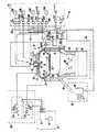
図1Aは本発明による誘電層を堆積させることができる高密度プラズマ化学気相堆積(HDV−CVD)システム10の1つの実施の形態を示している。システム10はチャンバ13、真空システム70、ソース・プラズマ・システム80A、バイアス・プラズマ・システム80B、ガス伝送システム33、そしてリモート・プラズマ・クリーニング・システム50を含んでいる。
【0022】
チャンバ13の上部部分はドーム14を含んでおり、これは酸化アルミニウムや窒化アルミニウムなどのセラミック性誘電材料でつくられている。ドーム14はプラズマ処理領域16の上側境界を形成している。プラズマ処理領域16は基板17の上面と基板支持部材18によって下側で境界を形成している。
【0023】
ヒーター・プレート23とコールド・プレート24はドーム14の上に置かれ、熱的にそれに結合されている。ヒーター・プレート23とコールド・プレート24は約100℃から200℃の温度で約+10℃でドーム温度を制御できるようにしている。これによって、種々のプロセスのためにドーム温度を最適化できる。例えば、クリーニング及びエッチング・プロセスのためには堆積プロセスの場合よりドームを高めの温度にしておく方が望ましい場合がある。ドーム温度を正確に制御することはさらにチャンバー内でのフレークや粒子の数を減少させ、堆積された層と基板との間の接着を強化してくれる。
【0024】
チャンバ13の下側部分はチャンバを真空システムに結合する部材22を含んでいる。基板支持部材18のベース部分21は部材22と共に連続的な内部表面を形成している。基板はチャンバー13内の挿入/取り出し開口部(図示せず)を通じてロボット・ブレートによってチャンバ13に出し入れされる。リフト・ペン(図示せず)はモーター(これも図示せず)の制御下で上げ下げされ、低取り付け位置57のロボット・ブレードから上記基板が基板支持部材18の基板受け取り位置19上に基板が載置されるより低い取り付け位置に移動される。基板受け取り部分19は基板処理中に基板を基板支持部材19に固定させる静電チャック20を含んでいる。1つの好ましい実施の形態においては、基板支持部材18は酸化アルミニウムまたは窒化アルミニウムによってできている。基板支持部材18は通常基板17の温度を調節するための加熱及び冷却要素を備えている。例えば、基板支持部材18は抵抗性ヒーターなどの加熱要素を含んでいる。また、基板17はチャンバ13内でプラズマからのイオンを用いてエネルギー照射を行うことで加熱することができる。多くの場合、基板支持部材18は冷却液用の導管など熱交換要素を含んでいる。基板受け取り部分19はバックサイド・ガス(例えばヘリウムな)などの熱伝達媒体を流通させるための溝または通路を含んでいる場合もある。この熱伝達媒体は真空よりも高い熱伝導性を有しており、それによって基板18部材と基板17との間の熱伝達を容易に行うことができる。
【0025】
真空システム70はスロットル体25を含んでおり、これはツイン・ブレード・スロットル弁26を収容しておりガス弁27及びターボ分子ポンプ28を開閉するために取り付けられている。なお、スロットル弁25はガス流に対しては最小限の障害にしかならず、参照によって本明細書に組み入れられている1995年12月12日出願の同様に譲渡された米国特許出願第08/574,839に述べられているようなシンメトリックなポンピングを可能にしてくれる。ゲート弁27はスロットル弁25からポンプ28を切り離すことができ、同時に、スロットル弁26が十分に開かれた場合排気流要領を制限することもできる。スロットル弁、ゲート弁、及びターボ分子ポンプの構成は約1ミリトール−2トールとの間の範囲内でチャンバ圧力の正確で安定した制御を可能にしてくれる。
【0026】
ソース・プラズマ・システム80Aはドーム14上に取り付けられたトップ・コイル29とサイド・コイル30を含んでいる。左右対称のグランド・シールド(図示せず)は上記コイル間の電気的結合を減少してくれる。このトップ・コイル29はトップ・ソースRF(SRF)発生装置31Aによって駆動され、一方、サイド・コイル30はサイドSRF発生装置によって駆動されるので、各コイルの作動の電力レベルと頻度をそれぞれ独立に制御することができる。この二重コイル・システムはチャンバ13内のラジアル・イオン密度を制御できるようにしてくれ、それによってプラズマの均一性を改善してくれる。サイド・コイル30とトップ・コイル29は通常誘導的に駆動され、これによって補足的な電極は必要とされない。1つの具体的な実施の形態で、上記トップ・ソースRF発生装置31Aは規格2MHzで最大5,000ワットのRF電力を提供する。トップ及びサイドRF発生装置の作動周波数はプラズマ発生効率を改良するために規格作動周波数(例えば、それぞれ1.7−1.9MHzと1.9−2.1MHz)からずれていてもよい。
【0027】
バイアス・プラズマ・システム80BはバイアスRF(BRF)発生装置31Cとバイアス・マッチング・ネットワーク32Cを含んでいる。バイアス・プラズマ・システム80Bは相補的電極として機能する基板部分17を部材22に容量的に結合されている。一般的に、BRF発生装置32Cは基板支持部材18、あるいは基板受け取り部材19または静電チャック20内のバイアス電極によって結合されている。
このバイアス・プラズマ・システム80Bは上記ソース・プラズマ・システム80Aによってつくられたプラズマ種(例えばイオン)の上記基板表面への移送の促進に寄与する。特殊な実施の形態では、バイアスRF発生装置は13.56MHzで最大5,000ワットのRF電力を提供する。
【0028】
RF発生装置31A及び31Bはデジタル的に制御されるシンセサイザを含んでおり、約1.8−約2.1MHzの範囲の周波数範囲で作動する。各発生装置は上記チャンバとコイルからの反射電力を測定し、当業者であれば理解できるような最低反射電力を得るように作動頻度を調節するRF制御回路(図示せず)を含んでいる。RF発生装置は通常50オームの特性インピーダンスで作動するように設定されている。RF電力は上記発生装置とはことなった特性インピーダンスを有する負荷から反射される場合もある。これはその負荷に伝達される電力を低下させる場合もある。さらに、その負荷から発生装置へ反射される負荷は過負荷を引き起こしてその発生装置を破損してしまう場合もある。プラズマのインピーダンスは種々の要因の中でもとりわけイオン密度によって5オーム以下から900オーム以上の範囲にわたっており、そして、反射電力は周波数の関数であるので、反射電力に応じて発生装置周波数を調製するとRF発生装置からプラズマに伝達される電力が増大させ、その発生装置を保護する。反射電力を減少させ、効率を向上させる別の方法はマッチング・ネットワークを用いる方法である。
【0029】
マッチング・ネットワーク32Aと32Bは発生装置31A及び31Bの出力インピーダンスをそのそれぞれのコイル29及び30と合わせる。RF制御回路は負荷が変わると発生装置をその負荷に合わせるためにマッチング・ネットワーク内のコンデンサの値を変えることで両方のマッチング・ネットワークを調整することができる。RF制御回路は負荷から発生装置へ反射される電力が一定の限界を超えた場合にマッチング・ネットワークを調整することができる。定常的なマッチングを実現してRF制御回路が有効にマッチング・ネットワークを調整できなくする1つの方法は反射電力のいずれかの予想値より上の反射電力限度を設定することである。これはほとんどの状況でマッチング・ネットワークを一定にすることでプラズマを一定の常態に安定化させるのに役立つ。
【0030】
他の手段もプラズマを安定させるのに役立つ。例えば、RF制御回路を用いて負荷(プラズマ)に与えられる電力を判定することができるし、1つの層の堆積中に伝達される電力をほぼ一定化するために発生装置の出力電源を増減することもできる。
【0031】
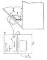
ガス伝達システム33はいくつかの供給源34A−34Fからのガスをガス伝送ライン38(その一部だけを図示)経由で基板を処理するためのチャンバに伝送する。当業者であれば容易に理解できるであろうが、供給源34A−34fのために用いられる実際の供給源とチャンバ13への伝送ライン38の実際の接続は一部にはそのチャンバ13内で行われるプロセスにも依存している。ガスはガス・リング37とトップ・ノズル45を通じてチャンバ13に導入される。図1Bはチャンバ13の簡略化された部分的断面図で、ガス・リング37のさらなる詳細を示している。
【0032】
1つの実施の形態で、第1及び第2のガス供給源34Aと34B、及び第1と第2のガスフローコントローラ35A'と35B'はガス伝送ライン38(部分的にしか図示せず)を経由してガス・リング37内のリング・プレナム36にガスを提供する。ガス・リング37は基板上に均一のガス流を提供する複数のソース・ガス・ノズル39(部分的にのみ図示)を有している。ノズルの長さとノズルの角度は1つのチャンバ内での特定のプロセスのために均一性特性とガス利用効率を調整できるようにするために変えることができる。1つの好ましい実施の形態で、ガス・リング37は酸化アルミニウム・セラミックスでできた12のソース・ガス・ノズルを有している。
【0033】
ガス・リング37も複数の酸化剤ガス・ノズル40(部分的にのみ図示)を有しており、これは1つの好ましい実施の形態で、ソース・ガス・ノズル39と共平面上にあり、その長さはソース・ガス・ノズル39より短く、そして1つの実施の形態でプレナム41からガスを受け取る。いくつかの実施の形態で、ガスをチャンバ13に注入する前に、ソース・ガスと酸化剤ガスを混合しない方が好ましい。他の実施の形態で、プレナム41とガス・リング・プレナム36との間に開口部(図示せず)を設けることによってソース・ガスと酸化剤ガスをチャンバ13内に注入する前に混合した方がよい場合もある。1つの実施の形態で、第3及び第4のガス供給源34C及び34D及び第3及び第4のガスフローコントローラ35C及び35D'はガス伝送ライン38を介してプレナムにガスを提供する。窒素源34Fは窒素プラズマを利用したプロセス・ステップのためにガスフローコントローラ35Fを介してガス・リングの酸化剤ノズル40に、そしてさらにチャンバへと窒素ガス(N2)を供給する。また、窒素ガスはガスフローコントローラ35F'を介してトップ・ノズル45など他の、あるいは追加的な取入口を通じてチャンバに供給することもできるであろう。43Bなどの追加的な弁で流れコントローラからチャンバへのガスを遮断するようにすることもできる。
【0034】
引火性、毒性、あるいは腐食性ガスが用いられるような実施の形態においては、堆積後、ガス伝送ライン内に残留しているガスを除去するのが望ましい。これはチャンバ13を伝送ライン38Aから切り離して、伝送ライン38Aを真空フォアライン44に排気するための、例えば弁43Bなどの3方向弁を用いて達成することができる。図1Aに示されているように、43A及び43Bなど他の同様の弁を他の35A及び35Cなどのガス伝送ライン上に組み込むこともできる。こうした3方向弁は(3方向弁とチャンバの間の)ガス伝送ラインから排気されないガスの体積を減少させるためにチャンバ13にできるだけ近づけて配置することができる。さらに、2方向(ON/OFF)弁(図示せず)をMFCとチャンバの間、あるいはガス供給源とMFCとの間に配置することもできる。
【0035】
図1Aで、チャンバ13はまたトップ・ノズル45とトップ・ベント46も有している。トップ・ノズル45とトップ・ベント46はガスのトップ及びサイド・フローをそれぞれ独立に制御することを可能にしてくれ、それによって膜の均一性が向上されると同時に、その膜堆積およびドーピングに関するパラメータを微調整できるようにしてくれる。トップ・ベント46はトップ・ノズル45の周りの環状開口部である。1つの実施の形態で、第1のガス供給源34Aはソース・ガス・ノズル39とトップ・ノズル45にガスを供給する。ソース・ノズル質量フローコントローラ(MFC)35A'はソース・ガス・ノズル39に提供されるシランの量を制御し、トップ・ノズルMFC35Aはトップ・ガス・ノズル45に提供されるシランの量を制御する。同様に、2つのMFC35B及び35B'を用いてソース34Bなど1つの酸素源からトップ・ベント46及び酸化剤ガス・ノズル40の両方への酸素の流れを制御することも可能である。トップ・ノズル45及びトップ・ベント46に供給されるガスはガスをチャンバ13内に流し込む前には別々にしておくことができるし、あるいはそれらがチャンバ13内に流れ込む前にトップ・プレナム48内で混合してもよい。チャンバのいろいろな場所に供給するために同じガスの別の供給源を用いても差し支えない。
【0036】
チャンバ成分から発生する堆積残留物を定期的に洗浄するためにリモート超短波発生プラズマ・クリーニング・システム50が設けられている。このクリーニング・システムはリアクタキャビティー53内の、フッ素分子、フッ化窒素、その他の炭素フッ化物やその相当物など洗浄ガス源34Eからプラズマをつくりだすリモート超短波発生装置51を含んでいる。このプラズマからもたらされる反応性種がアプリケータ・チューブ55を介し、洗浄ガス・フィード・ポート54を通じてチャンバ13に送られる。クリーニング・プラズマを入れるために用いられる(例えばキャビティー53とアプリケータ・チューブ55などの)素材はプラズマによる攻撃に対して抵抗性のあるものでなければならない。反応キャビティー53とフィード・ポート54は反応キャビティー53からの距離が長くなるにつれて望ましいプラズマ種の濃度が低下するので、できるだけ短くするべきである。リモート・キャビティー内でクリーニング・プラズマを発生させると効率的な超短波発生装置の使用が可能になり、チャンバ構成要素がin situプラズマの場合に存在するようなグロー放電の熱、放射、あるいは照射にさらされなくてすむ。結果として、静電チャック20などのような比較的影響を受け易い構成要素を、in situプラズマ洗浄プロセスで必要とされるようにダミー・ウエハで覆ったり、あるいはその他の手段で保護しなくてもよい。
【0037】
システムコントローラ60はシステム10の作動を制御する。1つの好ましい実施の形態においては、コントローラ60はハード・ディスク・ドライブ、フロッピー・ディスク・ドライブ(図示せず)、及びカード・ラック(図示せず)などの記憶装置62を含んでいる。カード・ラックは単一ボード・コンピュータ(SBC)(図示せず)、アナログ及びデジタル入力/出力ボード(図示せず)、インターフェース・ボード(図示せず)、及びステッパー・モーターコントローラボード(図示せず)などを含んでいる場合がある。システムコントローラはボード、カード・ケージ、及びコネクタ寸法及びタイプを規定するVersa Modular European(VME)標準に準拠している。VME標準は16ビット・データ・バス及び24−ビット・アドレス・バスを有するバス構造も定義している。システムコントローラ60はハード・ディスク・ドライブ上に保存されるコンピュータ・プログラムやフロッピー・ディスク上に保存されるプログラムなど他のコンピュータ・プログラムの制御下で作動する。コンピュータ・プログラムは、例えば、タイミング、ガスの混合、RF電力レベル、及び特定のプロセスのその他のパラメータを指令する。ユーザーとシステムコントローラとの間のインターフェースは図1Cに示されているように陰極線チューブ(CRT)65などのモニターとライト・ペン66を介している。
【0038】
図1Cは図1Aに例として示すCVD処理チャンバと結合して用いられる具体的なシステム・ユーザー・インターフェースの一部を示している。システムコントローラ60は記憶装置62に結合されたプロセッサ61を含んでいる。好ましくは、メモリー62はハード・ディスク・ドライブであるが、もちろん記憶装置62はROM、PROM、EPROM、CD−ROM、テープ・ドライブ、フロッピー・ディスク・ドライブなどの別のタイプの記憶装置であってもよい。
【0039】
システムコントローラ60はコンピュータ・プログラムの制御下で作動する。コンピュータ・プログラムはタイミング、温度、ガス・フロー、RF電力レベル、及び特定のプロセスのその他のパラメータを指令する。。ユーザーとシステムコントローラとの間のインターフェースは図1Cに示されているように陰極線チューブ(CRT)65とライト・ペン66を介している。1つの好ましい実施の形態においては、2つのモニター65と65Aが用いられ、1つはオペレータのためにクリーン・ルーム壁面(65)上に取り付けられ、他方は保守技術者のために壁面(65A)に取り付けられている。両方のモニターとも同じ情報を同時に示すことができるが、ライト・ペン(例えば66)は1つだけしか使えない。特定のスクリーンや画面を選択するために、オペレータはペンで表示画面の1つのエリアを触れ、ボタン(図示せず)を押す。触れられたエリアはライト・ペンの色が変わったり、あるいは例えば新しいメニューを表示するなどして、選択されたことを確認する。
【0040】
コンピュータ・プログラム・コードは68000アセンブリ言語、C、C++、Pascalなど従来のいずれのコンピュータ読み取り可能言語ででも書くことができる。
適切なプログラム・コードは通常のテキスト・エディターを用いて1つのファイル、あるいは複数のファイルに入れられ、そのコンピュータのメモリー・システムなどコンピュータで使用可能な媒体で保存される。入れられたコード・テキストが高レベルの言語で書かれている場合は、そのコードはコンパイルされ、得られたコンピュータ・コードはその後予めコンパイルされたウィンドウ・ライブラリ・ルーチンのオブジェクト・コードと結合される。結合されたコンパイルされたオブジェクト・コードを実行するためには、システム・ユーザーがオブジェクト・コードを起動させると、コンピュータ・システムがそのコードを記憶装置内にロードし、そこから、CPUはそのプログラム内に識別されているタスクを実行するためにコードを読み出して実行する。
【0041】
図1Dコンピュータ・プログラム70の階層的制御構造を示す構成図である。ユーザーはライト・ペン・インターフェースを用いてCRTモニター上に表示されたメニューや画面に対応してプロセス・セット番号とプロセス・チャンバ番号を入力する。プロセス・セットは特定のプロセスを実行するのに必要なプロセス・パラメータの予め決めたセットであり、予め決められたセット番号で識別される。
プロセス・セレクタ・サブルーチン73は(i)多重チャンバ・システム内の望ましいプロセス・チャンバと、(ii)望ましいプロセスを実行するためにそのプロセス・チャンバを作動させるのに必要なプロセス・パラメータの望ましいセットを表示する。特定のプロセスを実行するためのプロセス・パラメータは、例えば、プロセス・ガス組成及び流量、温度、圧力、RF電力レベルなどのプラズマ条件、そしてチャンバ・ドーム温度などのプロセス条件と関連しており、レシピの形状でユーザーに提供される。レシピで指定されたパラメータはライト・ペン/CRTモニター・インターフェースを用いて入力される。
【0042】
そのプロセスをモニタリングするための信号はシステムコントローラのアナログ入力及びデジタル入力ボードによって提供され、そのプロセスを制御するための信号はシステムコントローラ60のアナログ出力及びデジタル出力ボード上で出力される。
【0043】
プロセス・シーケンサー・サブルーチン75は表示されたプロセス番号とプロセス・パラメータのセットをプロセス・セレクタ・サブルーチン73から受け取り、種々のプロセス・チャンバの作動を制御するためのプログラム・コードで構成されている。複数のユーザーがプロセス・セット番号とプロセス・チャンバ番号を入力することができ、あるいは、ひとりのユーザーが複数のプロセス・セット番号とプロセス・チャンバ番号を入力することができるので、シーケンサー・サブルーチン75は選択されたプロセスを望ましい順番で実行するように作動する。好ましくは、シーケンサー・サブルーチン75は(i)チャンバが使用中かどうかを判定するためにそのプロセス・チャンバをモニタリングするステップと、(ii)使用中のチャンバでどのプロセスが実行されているかを判定するステップと、(iii)プロセス・チャンバの利用可能性と実行されるべきプロセスのタイプに基づいて望ましいプロセスを実行するステップ、を実行するためのプログラム・コードを含んでいる。ポーリングなど、プロセス・チャンバをモニタリングするための従来の方法を使用することができる。どのプロセスを実行すべきかスケジュールを決める場合、シーケンサー・サブルーチン75は使用中のプロセス・チャンバの現在の条件を選択されたプロセスにとって望ましいプロセス条件との比較したり、各ユーザー入力リクエストの『エイジ(年齢)』あるいはシステム・プログラマがスケジュール上の優先順位を判定するために含めたいと思う他の適切なファクターを考慮するように設定することができる。
【0044】
シーケンサー・サブルーチン75がどのプロセス・チャンバとプロセス・セット番号の組み合わせを次に実行すべきかについて判定したら、シーケンサー・サブルーチン75はシーケンサー・サブルーチン75によって決められたプロセス・セットに従って種々のプロセス・チャンバ(図示せず)内の複数の処理タスクを制御するチャンバ・マネジャー・サブルーチン77a−77cに特定のプロセス・セット・パラメータを送ることによって、そのプロセス・セットを実行させる。特にチャンバ・マネジャー・サブルーチン77aは図1AのHDP−CVDチャンバなどCVDチャンバを制御する。
【0045】
チャンバ構成要素サブルーチンの実例としては基板位置決めサブルーチン80、プロセス・ガス制御サブルーチン83、圧力制御サブルーチン85、ヒーター制御サブルーチン87、そしてプラズマ制御サブルーチン90である。当業者であれば、チャンバ13内でどのようなプロセスの実行を望むかに応じて、他のチャンバ制御サブルーチンを含めることができることは容易に理解できるであろう。作動中、チャンバ・マネジャー・サブルーチン77aは実行されている特定のプロセス・セットに従って、プロセス構成要素サブルーチンをスケジュールしたりコールしたりすることができる。チャンバ・マネジャー・サブルーチン77aによるスケジューリングはシーケンサー・サブルーチン75がどのプロセス・チャンバとプロセス・セットを実行すべきかを決める際に用いるのと同様の方法で行われる。通常、チャンバ・マネジャー・サブルーチン77aは種々のチャンバ構成要素をモニタリングしたり、実行すべきプロセス・セットのためのプロセス・パラメータに基づいてどの構成要素を作動させるべきかを判定し、そして、モニタリング及び判定ステップに対応するチャンバ構成要素サブルーチンを実行させたりするステップを含んでいる。
【0046】
特定のチャンバ構成要素サブルーチンの動作について図1Dを参照して以下に説明する。基板位置決めサブルーチン80は基板を基板支持部材18上に載せるために用いられるチャンバ構成要素を制御するためのプログラム・コードを含んでいる。基板位置決めサブルーチン80は、他の処理が完了した後、多重チャンバ・システム内のPECVDまたは他のリアクタからチャンバ13への基板の移送も制御する。
【0047】
プロセス・ガス・サブルーチン83はプロセス・ガス組成と流量を制御するためのプログラム・コードを有している。サブルーチン83は安全遮断弁の開放/閉鎖位置を制御し、望ましいガス流量を得るために質量フローコントローラをランプ・アップ/ダウンすることができる。プロセス・ガス制御サブルーチン83を含めすべてのチャンバ構成要素サブルーチンはチャンバ・マネジャー・サブルーチン77aによって起動される。サブルーチン83はチャンバ・マネジャー・サブルーチン77aから望ましいガス流量に関連したプロセス・パラメータを受け取る。
【0048】
典型的に、プロセス・ガス制御サブルーチン83は、ガス供給ラインを開き、(i)必要な質量フローコントローラを読み取り、(ii)チャンバ・マネジャー・サブルーチン77aから受け取った望ましい流量の読み取り値を比較し、そして(iii)必要に応じてガス供給ラインの流量を調整するステップを繰り返すことで作動する。さらに、プロセス・ガス制御サブルーチン83はガス流量が安全かどうかをモニターして、安全でない状態が検出されたら安全遮断弁を作動させるステップを含んでいる場合もある。
【0049】
いくつかのプロセスで、反応性のプロセス・ガスがチャンバに導入される前に、そのチャンバ内の圧力を安定化させるためにアルゴンなどの不活性ガスがチャンバに導入される。これらのプロセスのために、プロセス・ガス制御サブルーチン83はそのチャンバ内の圧力を安定化させるために必要な時間チャンバ13内に不活性ガスを流入させるステップを含むようにプログラムされる。その後、上に述べたステップを実行することができる。
【0050】
さらに、プロセス・ガスを例えばテトラエチルオキシシラン(TEOS)などの液体前駆体から蒸発させることが必要な場合は、プロセス・ガス制御サブルーチン83はバブラー・アセンブリ内でその液体前駆体を通じてヘリウムなどのデリバリ・ガスを泡立てたり、あるいはヘリウムを液体注入弁に導入したりするためのステップを含んでいてもよい。このタイプのプロセスの場合、プロセス・ガス制御サブルーチン83は望ましいプロセス・ガス流量を得るためにデリバリ・ガスのフロー、バブラー内の圧力、バブラー温度を調節する。上に述べたように、望ましいプロセス・ガス流量は圧力パラメータとしてプロセス・ガス制御サブルーチン83に送られる。
【0051】
さらに、プロセス・ガス制御サブルーチン83は一定のプロセス・ガス流量のために必要な値を含む保存されたテーブルにアクセスして、望ましいプロセス・ガス流量のために必要なデリバリ・ガス流量、バブラー圧力、及びバブラー温度を得るステップを含んでいる。必要な値が得られたら、デリバリ・ガス流量、バブラー圧力、及びバブラー温度がモニターされて、必要な値と比較され、必要に応じて調節される。
【0052】
プロセス・ガス制御サブルーチン83はさらにウエハ・チャック内の内側及び外側通路を通じてのヘリウム(He)などの熱伝達ガスのフローを独立のヘリウム制御(HC)サブルーチン(図示せず)で制御することもできる。このガス流はその基板をチャックに熱的に接合させる。一般的なプロセスにおいては、そのプラズマとその層を形成する化学反応はウエハを加熱し、そして、Heはチャックを通じて基板を冷却するが、これは水で冷却されてもよい。これは基板をその基板上の予め存在しているフィーチャーを損傷する可能性のある温度以下に保持する。
【0053】
圧力制御サブルーチン85はそのチャンバの排気部分のスロットル弁の開口部のサイズを調整することでチャンバ13内の圧力を制御するためのプログラム・コードを含んでいる。スロットル弁でチャンバを制御するためには少なくとも2つの基本的な方法が存在する。第1の方法は、チャンバ圧力がとりわけ総プロセス・ガス・フロー、プロセス・チャンバのサイズ、及びポンピング容量と関連しているので、そのチャンバ圧力の特徴づけに依存している。第1の方法は弁26を固定位置に設定する。スロットル弁26を固定位置に設定することは安定した圧力につながる。
【0054】
また、チャンバ圧力は、例えばマノメータで測定することができ、スロットル弁26の位置は制御ポイントがガス流及び排気容量で設定される境界内にあれば圧力制御サブルーチン85に従って調整することができる。前の方法は後者の方法に関連しているような測定、比較、計算などの作業を必要としないので、より迅速にチャンバ圧力を変化させることができる。チャンバ圧力の正確な制御が必要ではない場合は前者の方法が望ましく、層の堆積中などのように正確で、反復可能で、そして安定した圧力が必要な場合は後者の方法が望ましい。
【0055】
圧力制御サブルーチン85が起動されると、望ましい、あるいは目標とする圧力レベルがチャンバ・マネジャー・サブルーチン77aからのパラメータとして受け取られる。圧力制御サブルーチン85はそのチャンバに接続された1つまたは複数の通常の圧力マノメータで読み取ることでチャンバ13内の圧力を測定し、その測定値を目標圧力と比較し、目標圧力に対応して保存された圧力テーブルから比例的、積分、及び微分(PID)値を得て、圧力テーブルから得られたPID値に従ってスロットル弁26を調節するように作動する。また、圧力制御サブルーチン85はチャンバ13内の圧力を望ましい圧力あるいは圧力範囲に調節するために特定の開口部サイズに合わせてスロットル弁26を開閉することができる。
【0056】
ヒーター制御サブルーチン87は基板の温度及び/またはチャンバ13内の温度を制御するためのプログラム・コードを含んでいる。チャンバ温度を制御するためには少なくとも2つの基本的な方法がある。第1の方法は基板温度に依存しているが、それは基板温度がとりわけプラズマによって与えられる力全体に関係しているからである。第1の方法はソースRF電力及び/またはバイアスRF電力のレベルを調節する。電力レベルを増大させると、一般的には基板温度も上昇する。電力レベルを低下すると、通常は基板温度も低下する。第1の方法はチャンバ13の温度を制御するためにも用いることができる。
【0057】
また、チャンバまたは基板温度を熱伝対またはパイロメータで測定することができ、温度は別の温度コントローラで制御される。そうした温度コントローラはヒーター要素、冷却要素、あるいはその両方を含んでいる。そうした加熱/冷却要素は基板支持部材18、チャンバ13または両方に結合することができる。一部チャンバはドーム14のための別の温度コントローラを含んでいる。
【0058】
温度制御サブルーチン87が起動されると、望ましい、あるいは目標とする圧力レベルはチャンバ・マネジャー・サブルーチン77aからパラメータとして受け受け取られる。温度制御サブルーチン87はチャンバ及び/または基板に接続された1つまたは複数の通常の温度センサーを読み取ることでチャンバ13または基板17の温度を測定し、測定値を目標温度と比較し、保存された圧力テーブルから上記目標圧力と対応した比例的、積分、及び微分(PID)を得、圧力テーブルから得られたPID値に従ってソースRF発生装置31A、バイアスRF発生装置31B、そしてチャンバ/基板加熱/冷却要素の一定の組み合わせを調節するように作動する。また、温度制御サブルーチン87はソースRF発生装置31A及び/またはバイアスRF発生装置31Bを特定の電力レベルに設定して基板17の温度を望ましい温度または温度範囲に調節することができる。
【0059】
プラズマ制御サブルーチン90はRF発生装置31A及び31Bの周波数及び電力出力設定を制御するため、及びマッチング・ネットワーク32A及び32Bを調整するためのプログラム・コードを含んでいる。プラズマ制御サブルーチン90は前に述べたチャンバ構成要素サブルーチンの場合と同様、チャンバ・マネジャー・サブルーチン77aによって起動される。当業者であれば、プラズマの制御によって基板温度を調節する場合、温度制御サブルーチン87をプラズマ制御サブルーチン90内に全体的、あるいは部分的に組み込むことができることは理解できるであろう。
【0060】
上に述べたサブシステム及びルーチンの一部あるいは全てを組み込んだシステムの例は本発明を実行するように構成されたApplied Materials社によって製造されたUltima Systemであろう。こうしたシステムの詳細は共同発明者として、Fred C. Redeker, Farhad Moghadam, HIrogi Hanakawa , Tetsuya Ishikawa , Dan Maydan, Shijian Li, Brian Lue, Robert Steger, Yaxin Wang, Manus Wong, and Ashok Sinhaが共同発明者としてリストアップされ、1996年7月15日に提出された『左右対称的に調節可能な誘導的に結合されたHDP−CVDリアクタ』と題する米国特許出願第08/679,927に開示されており、その開示は参照によって本明細書に組み込まれる。
【0061】
III. 例示的構造
図2は本発明による集積回路200の簡略化さえた断面図を示す。図2に示されているように、集積回路200はNMOS及びPMOSトランジスタ203及び206を含んでおり、これらはフィールド酸化物領域220によって相互に分離され、電気的に切り離されている。トランジスタ203及び206のそれぞれはソース領域212、ドレイン領域215、及びゲート領域118を含んでいる。
【0062】
プレメタル誘電層221はトランジスタ203及び206を金属層240から切り離しており、金属層230とトランジスタ203、206間の接続は接触子224によって行われる。
金属層240は、例えば、集積回路200内に含まれている4つの金属層240、242、244、及び246のうちの1つである。各金属層はバリア層227a、228a、ギャップ・フィル層227b、228b、229b、及びキャップ層227c、228c、229cを含む金属間誘電(IMD)層227、228、及び229によって隣接する金属層から分離されている。隣接金属層はヴィアス226によって選択された開口部で接続されている。堆積されたオーバー金属層246は、例えば、バリア層230a、ギャップ・フィル層230b、及びキャップ層230cを含む平面化された不動体化層230である。
【0063】
好ましくは、ギャップ−フィル層227b、228b、229b、及び230bの少なくとも1つは本発明の第1の実施の形態に従って酸素で処理されたFSGを含んでいる。
キャップ層227c、228c、229c及び230cの少なくとも1つが本発明の第2の実施の形態による低圧ストライクを用いて堆積されるのがより好ましい。上記第1の実施の形態に従って酸素で処理されたギャップ−フィル層上に第2の実施の形態によるキャップ層を堆積させるのが最も好ましい。
【0064】
本発明による層は集積回路200内に示されている誘電層のそれぞれで利用することができるであろう。本発明による層はダマシン層でも使うことができる。ダマシン層では、ブランケット沿うが基板上に堆積され、基板に至るまで選択的にエッチングされ、そして、金属を充填させ、エッチ・バックあるいは研磨されて224などの金属接触子を形成する。金属層が堆積された後、第2のブランケット堆積が行われ、選択的にエッチングされる。エッチングされた領域はその後金属を充填され、エッチ・バックまたは磨かれて226などのヴァイアスを形成する。
【0065】
なお、簡略化された集積回路100は説明目的のためだけである。当業者であればマイクロプロセッサ、アプリケーション固有集積回路(ASIC)、記憶装置など他の集積回路の製造に本発明を適用することができるであろう。
【0066】
IV.例示的低誘電率膜
本発明の実施の形態に従って堆積された誘電膜は一般的には低い誘電率を持っている。誘電率が低いということはここではドーピングされていない酸化ケイ素膜の誘電率より低いことを意味している。一般的に、酸化ケイ素(SixOy)の誘電率kは約4である。kが4以上の膜は高k膜と呼ばれる。低誘電率はフルオロケイ酸塩ガラス(FSG)の層を形成するためにその膜の酸化ケイ素層に組み込まれるフッ素原子によってもたらされる。こうした誘電膜は金属間誘電体(IMD)膜あるいはその他のタイプの誘電体層として用いることができる。以下の具体的例は銅トレース上に形成されたIMD層を示しており、これらは合わせても0.25ミクロンの厚さで、アスペクト比は4:1である。この膜は薄い窒化ケイ素層を有しており、これはFSGに強力に接着している。窒化ケイ素層は銅とFSG層との間の分散バリアとして機能する。従って、この層は誘電率が低くなっているばかりでなく、優れたギャップ充填性も有しており、半導体基板上で予め存在している銅構造との共存性においても優れている。
【0067】
図3は2層酸化ケイ素膜300を有する本発明の1つの実施の形態の簡略断面図である。窒化ケイ素、例えばSi3N4などのHDP−CVD層302が伝導性トレース304、305及び基板306上に堆積されている。基板306は、例えば、シリコン・ウエハあるいは既存の構造あるいは層を有するシリコン・ウエハなどである。この窒化ケイ素層は拡散バリアとして機能し、同時に圧縮性の層で、特に金属クラッキング及び電子移行などの不具合に関してその下側にある金属トレースの信頼咳を高める役割を果たしている。窒化ケイ素層302は本発明の第2の実施の形態に従って堆積させることができる。FSGによるHDP−CVD層308は窒化ケイ素層302の表面310上に堆積される。FSG308は通常のHDP−CVDによって堆積された後、酸素312によって処理される。オプションとしてのキャップ層314を堆積させて、FSG層を密封し、その後で行われる一般的な半導体プロセスに耐えられるような表面をもたらすこともできる。好ましくはキャップ層314は本発明の第2の実施の形態に従って堆積された窒化ケイ素層である。
【0068】
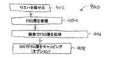
V.低誘電率膜の堆積
図4は酸素処理がFSG層の安定性を強化している本発明による堆積方法の1つの実施の形態のフロー・チャートである。この実施の形態で、この処理は1つの処理チャンバ内で行われるが、このプロセスは多重チャンバ・システムに対しても適用することができ、あるいは一連の異なったチャンバやシステムで行うこともできる。同様に、以下に述べるプロセス・パラメータは8インチ・プロセス・ウエハのためのものであるが、このプロセスは10インチ・ウエハなど他のウエハに対応できるように修正することもできる。
【0069】
ウエハは真空ロック・ドアあるいはスリット弁を通じて処理チャンバ内の基板支持部材上に載置され(ステップ402)、望ましい処理位置まで移動される。ケイ素源、フッ素源、及び酸素源を含むプロセス・ガスがそのチャンバに導入され、ウエハ上にFSG(ステップ404)の層を堆積させるために高密度プラズマが形成される。好ましい実施の形態において、ケイ素源はモノシラン(SiH4)であり、フッ素源はケイ素源とも考えられるテトラフルオロシラン(SiF4)であり、そして酸素源は二原子酸素(O2)である。また、TEOSあるいはジシラン(Si2H6)、トリシラン(Si3H8)、テトラシラン(Si4H10)などの他のシラン類もケイ素源として用いることもできる。同様に、F2などの他のガスもフッ素源として用いることができる。オゾン(O3)を別の酸素源として用いることも可能である。プラズマはオプションとしてヘリウムやアルゴンなどの不活性ガスを含むこともできる。一般的にはヘリウムよりアルゴン内での方がプラズマを発生させやすい。ネオン、クリプトン、あるいはキセノンなどの他の不活性ガスも用いることができるが、クリプトン及びキセノンはヘリウム及びアルゴンより高価になる傾向が強い。
【0070】
これらのガスは、SiF4の場合、1分間あたり90及び94標準立法センチメートル(Sccm)の範囲の流量で、SiH4の場合は50−54sccm、そしてO2の場合、155−165sccmの範囲の流量で提供される。ガス流量はより好ましくはSiF4の場合1分間あたり約94標準立法センチメートル(sccm)、SiH4の場合は50sccm、そしてO2の場合は160sccmである。チャンバ内の圧力は通常は約3.5−6ミリトールの範囲、好ましくは約4ミリトールに設定、保持される。プラズマは単一、あるいは混合周波数RF電力の適用によって形成することができる。一般的に、SRF発生装置31Aは約1.7−1.9Hzの範囲の周波数、好ましくは約1.8Hzの周波数、及び約800及び1000W、好ましくは約800Wの電力レベルで作動するRF電力トップ・コイル29を提供する。SRF発生装置31Bはサイド・コイル30に対して2.0MHz−2.1MHzの範囲の周波数、及び約2500−3500W、好ましくは約3000Wの範囲でRF電力を与える。バイアスRF電力は約13.56MHzの周波数と約800W−2000W、好ましくは1800Wの電力で基板17に提供される。ウエハ温度は通常380℃から400℃の範囲に保持される。チャンバ温度は通常約70−75℃の範囲、好ましくは約75℃に保持される。
【0071】
上記のプロセス条件は厚みが約6,000オングストロームから12,000オングストローム、好ましくは約8,000−10,000オングストロームのFSG層を形成するのに十分な時間維持される。実際の堆積時間が用いられるチャンバに依存する。例として、図1aから1dに示す例としてのチャンバの場合は、上のパラメータを用いて厚さ8000オングストロームのFSG層を約90秒で堆積させることができる。この段階で、上の条件で堆積されたFSG膜は比較的高い酸素に対するフッ素原子比を有している。好ましい実施の形態においては、FSG層は%PHRで測定してFSG層を酸素で処理する前の段階で約7.8%から約8.0%の範囲のフッ素濃度を有している。一般的に、O2/Si比率は約1.0−1.2の範囲であり、好ましくは1.1程度である。このO2/Si比率は以下に示すように、O2、SiF4、及びSiH4の流量に依存している。
O2/Si = O2(SiF4 + SiH4)
通常、SiF4/SiH4流量比率は約1.7−約1.8の範囲であり、好ましくは約1.75である。実際の流量は使用されるチャンバに依存している。
【0072】
FSG層の誘電率k及び屈折率nはFSG膜におけるフッ素の原子比率(パーセント)に依存している。通常、スッ素含有量が大きくなればなる程、k及びnの値は小さくなる。フッ素含有量が0at%程度のFSG膜、ドーピングされていないケイ酸塩ガラス(USG)は通常k値が約4、屈折率が約1.46である。FSG膜をフッ素で10at%程度までドーピングすると、屈折率は3.4−3.7の範囲となり、そして屈折率は1.40−1.43の範囲となる。膜の誘電率は通常は堆積された膜のキャパシタンス及び電圧(C−V)測定とk値が分かっている基準膜によって判定される。
【0073】
FSGを堆積させるための上に述べた方法に加えて、フッ素化シリコン・ガラス(FSG)を形成するためのいくつかの異なったプロセスが知られている。そうした別のプロセスの1つはPECVD堆積プロセスでトリエトキシフルオロシラン(TEFS)をテトラエチルオキシシラン(TEOS)と共に用いる。FSG膜を形成するさらに別のプロセスはPECVDプロセスにおいてフッ素源としてC2F6を用いる。そうしたFSG堆積プロセスはApplied Materialsに譲渡された米国特許出願第09/075,592に述べられている。
【0074】
FSG層を形成した後、FSG層の表面は酸素に対するフッ素の比率を低くするために酸素で処理される(ステップ406)。酸素処理は、例えば、酸素やオゾンへの露出中にFSG層を加熱したり、活発な酸素イオンまたは活発な中性酸素原子で照射することによって達成できる。1つの好ましい実施の形態においては、FSG層はその内部でFSGが堆積されたのと同じチャンバ内でプラズマからの酸素イオンによって照射される。通常、SiF4とSiH4フローはFSG堆積の終了時に停止され、一方、酸素流量はステップ404の場合のようにほぼ同様の水準に維持される。プラズマは堆積の際に用いられたのとほぼ同じソースRFに対する電力と周波数設定を用いて保持される。バイアスRF周波数は通常FSG堆積中と同様、酸素処理中同じ値を保持するが、BRF電力は堆積中に用いられた値より3分の1程度増大される。より好ましい実施の形態では、BRF電力は酸素処理中1500W−1800Wの範囲に保持される。
【0075】
酸素処理中、ウエハ温度は約420℃に維持される。チャンバ圧力は、約10秒から1分間、好ましくは20秒間程度、約1.8−2.5ミリトール、好ましくは約2ミリトールに保持される。処理システムを通じての高いウエハ処理量が望ましく、従って、十分な酸素処理を行いつつ、同時に処理時間はできるだけ短くする必要がある。必要となる正確な時間はその前のHDP−CVDがどのように行われたかも含めて多くのファクターに依存している。酸素はFSG層内に入り込み、そこでフッ素と反応して得られる膜をより安定なものとする。FSG層は%PHRで測定して、酸素による処理後、約7.5%から約7.8%程度の範囲のフッ素濃度を有している。
【0076】
オプションとして、窒化ケイ素キャップ層をFSG層上に堆積させてもよい(ステップ408)。このキャップ層は下側の層の低誘電率を達成するために必要ではないが、FSG層をその後で行われる集積回路処理ステップとより折り合いをよくしてくれる。FSG層はキャップ層形成の前に平面化、あるいは高密度化することができる。キャップ層は上に述べたプロセスと同様のHDP−CVDプロセスを用いて形成することができる。しかしながら、非常に薄い、例えば厚みが1000オングストローム以下の膜の堆積を制御するためには、プラズマを開始するために特別の低圧ストライクが必要である。
【0077】
VI.低圧ストライクを用いたキャップ層の堆積
FSG膜上に窒化ケイ素の薄いキャップ層を堆積させるのが好適である。ダマシンアプリケーションにおいては、銅上に堆積された窒化ケイ素は上側あるいは下側層内への銅の拡散に対するバリアとしての役割を果たす。また、FSGなどの誘電層上に堆積された窒化ケイ素はエッチング・ステップとしての役割も果たす。窒化ケイ素は約10%の原子%を含んだFSGの場合が3.4であるのに対してk値が約7程度であるので、窒化ケイ素の薄い層が望ましい。複合誘電層の有効な誘電率はその膜を構成する各層の厚さ及び誘電率に依存する。
一般的に、誘電率がそれぞれK1とK2、そして厚さがそれぞれd1とd2である2つの層で構成される膜の場合、その膜の有効誘電率Keffは各層の誘電率及び厚みに依存している。通常、より薄い層はその膜の有効誘電率により大きな影響を及ぼす。従って、窒化ケイ素はFSGよりずっと大きな誘電率を有しているが、窒化ケイ素層が全体的な膜厚と比較して十分に薄ければ、その膜の有効誘電率はFSGの誘電率に近づけることができる。
【0078】
薄いことに加えて、窒化ケイ素は通常均一でなければならない。FSG堆積後に均一な薄い窒化ケイ素層を堆積させるためには、しばしば堆積ガスを流動させながらプラズマを発火させることが望ましい。図5は低圧ストライクを用いて本発明によるキャップ層を堆積させる方法の1つの実施の形態のフロー図である。低圧ストライク法は本願と同時に出願され、参照によって本明細書に組み入れられ、共譲渡された、『HDP−CVDチャンバにおける低圧ストライク』と題する米国特許出願、弁理士整理番号AMAT/3272/PDD/KPU3/JWに十分に述べられている。図5に示されている方法の実施の形態は図4のステップ408の好ましい実施の形態である。この方法500は上に述べたようなFSG層の酸素処理後に開始される。別の方法として、ステップ404の後でキャップ層を方法500に従って堆積させてもよい。この方法はステップ502後に、フッ素、ケイ素、及び酸素源を遮断して開始される。しかしながら、いずれかの不活性ガス流はそのまま流動させておいてよい。前のステップで不活性ガスが用いられない場合は、不活性ガスの流れが他のガスを遮断する前に確立される。従って、不活性ガスのプラズマがチャンバ内で確立される。好ましい実施の形態においては、不活性ガスはアルゴンであり、180−200sccmの範囲の流量で提供される。ソースRFは通常トップ及びサイド・コイルのそれぞれに対して1.8Hzから2.07Hzの範囲の周波数に維持される。ソースRF電力は約4000W−5000Wの範囲、そして好ましくは約4500Wに維持される。バイアスRFはステップ504で不活性プラズマからのイオンが膜を照射する運動エネルギーを減らすためにOFFされる。
【0079】
基板温度はステップ506で確立される。窒化ケイ素(SixNy)のキャップ層の場合、通常、堆積を行う前に約430℃程度の基板温度が確立される。例えば、基板をプラズマに露出させるなど、基板を確立するために不活性プラズマだけを基板を加熱するために用いてもよい。露出時間はその基板のために必要な温度上昇幅に依存する。通常、基板が熱ければ熱い程、それを加熱する時間は短くて済む。処理量を増大させるためには、一般的に下側の層が堆積された後で、つまり、ウエハがすでに熱くなっている場合、できるだけ早くキャップ層を堆積させるのが好適である。例えば、FSG堆積後すぐにキャップ層を堆積させねばならない場合は、基板はすでにかなり熱くなっている。こうした状況においては、基板を不活性プラズマに約10秒間程度露出させれば、通常はキャップ層堆積のために基板を望ましい温度まで加熱するのに十分である。また、基板支持における加熱要素を単独あるいはプラズマと組み合わせて基板を加熱するために用いることができる。堆積のための望ましい温度が確立されたら、不活性ガスが依然として流れている状況でステップ508でソースRFをOFFする。ソースRFばなければ、チャンバ内にプラズマは存在しない。ソースRFがOFFされた瞬間に、堆積ガスがそのチャンバに導入されて、不活性ガスと混合される。SixNyキャップ層の場合、堆積ガスは通常はケイ素源と窒素源を含んでいる。1つの好ましい実施の形態で、ケイ素源はSiH4であり、窒素源は二原子窒素(N2)である。また、Si2H6などの他の有機シランをケイ素源として用いることができ、アンモニア(NH3)などの他の窒素含有ガスを窒素源として用いることができる。
【0080】
ステップ510で、堆積ガスの流量が確立される。SixNy堆積の好ましい実施の形態においては、SiH4流量は16から20sccmの範囲であり、N2流量は230から270sccmの範囲である。通常、ガス伝送システム内の質量フローコントローラがそれぞれの設定された流量を確率するために3から6秒間待機する必要がある。正確な待機時間はそのガス伝送システム内の個別質量フローコントローラに依存する。チャンバ圧力もこの時点で確立される。低圧ストライクの場合、チャンバ圧力は通常1から100ミリトールの範囲である。好ましくはチャンバ圧力は約40ミリトール未満である。窒化ケイ素堆積の場合、チャンバ内の圧力は通常この段階で4から7ミリトールの範囲である。
【0081】
なおステップ502から508まではオプション可能である。これらのステップは同じチャンバで下側の層の堆積が終了した直後にインサイチュ(in situ)でキャップ層を堆積させるために低圧ストライクが用いられるような特別の場合に用いられる。また、低圧ストライク法はステップ510におけるようにガス流量及びチャンバ圧力の安定化と同時に開始することができる。
【0082】
流量とチャンバ圧力が確立されると、ステップ512でチャンバ内で弱いプラズマが確立される。通常、約40ミリトール未満の圧力の場合、誘導的に結合されたプラズマより容量的に結合されたプラズマを確立する方がより簡単である。
弱いプラズマが確立されると、ソースRFがONされてステップ514で堆積プラズマが確立される。弱いプラズマという表現はそのプラズマ電力が基板上に形成される装置に対する損傷を回避するのに十分な低さであることを意味している。そうした弱い、容量的に結合されたプラズマは基板支持部材18に対して直流(DC)あるいはRFバイアスを負荷して電場を発生させることで確立することができる。1つの実施の形態において、容量的に結合された弱いプラズマは300W−1000Wの範囲の電力を最大0.1秒間のバイアス期間基板バイアス(例えば、BRF発生装置31C)をONすることで確立される。実際の電力はある程度処理される基板のサイズに依存する。例えば、200mm基板の場合、バイアス電力は好ましくは1500−2000ワットの範囲、好ましくは約1800Wである。対応する電力密度は好ましくは約4.8W/cm2−6.4W/cm2、より好ましくは約5.7W/cm2である。より大きな、あるいはより小さな基板の場合は、バイアス電力密度はほぼ同じ範囲であり、バイアス電力はウエハの表面積とほぼ比例している。
【0083】
一旦弱いプラズマが確立されると、ソースRFがONされてステップ514で堆積プラズマが確立され、そしてソースRFがONされるとすぐ基板バイアスがOFFされる。ソースRFがONされる前に基板バイアスがOFFされると、プラズマは通常消失してしまい、これは望ましくない。従って、通常ソースRFとバイアスRFの両方がONされる期間に多少のオーバーラップがある。通常このオーバーラップ期間はバイアス期間のほぼ後半に相当する。例えば、基板バイアスが0.5−1.0秒間のバイアス期間ONされると、ソースRFは基板バイアスがONされる最後の0.25−0.5秒にオーバーラップする期間ONされる。通常、バイアス期間とオーバーラップ期間はできるだけ短くするのが望ましい。バイアス期間とオーバーラップ期間の下限は通常発生装置の応答速度と基板バイアス及びソースRF信号の電子的特性に依存する。
【0084】
キャップ層は堆積プラズマを用いてステップ516で堆積される。通常、基板バイアスは窒化ケイ素堆積中はONされる。バイアスRFは酸化ケイ素など他の堆積プロセス中に用いられることも時々ある。ガスの流量とRF設定、及びチャンバ圧力が決まると、堆積されるキャップ層の厚さは堆積時間に大きく依存する。 一般的に、堆積時間が長くなると、膜はより薄くなる。堆積ガスの流量はプラス間発生の前に確立されているので、最初の堆積は先行技術におけるより均一性が高まる。結果的に1000オングストローム以下の非常に均一な膜を堆積させることができる。最も好ましい実施の形態においては、流量はArの場合200sccm、SiH4の場合18sccm、そしてN2の場合250sccmであり、ソースRFは約4500Wの総電力、そしてチャンバ圧力は約7−8ミリトールである。これらの条件の下で、堆積時間を50秒から60秒とすると、厚さが800−1000オングストロームのSixNy膜が形成される。ここで述べられているような低圧ストライクを用いて堆積された窒化ケイ素膜はその不均一性が2.25%と非常に低い。この均一性は先行技術と比較してかなり高い。さらに、低圧ストライクで堆積された膜の非不均一性は堆積が開始されてから最大で少なくとも65秒間程度保持される。従って、低圧ストライクを用いて堆積された非常に薄い膜(例えば、約300オングストローム)でも非常に均一である。
【0085】
本発明による方法の1つの実施の形態をFSG層上に窒化ケイ素キャップ層を堆積させる例を参照して上に説明したが、その基本的範囲を逸脱せずに他の、そしてさらに別の本発明の実施の形態を考案することは可能である。例えば、FSG堆積ステップと窒化ケイ素堆積ステップを逆にすることができる。つまり、薄い(<1000オングストローム)窒化ケイ素層を上に図5を参照して説明したように低圧ストライクを用いて基板上に堆積させ、そしてFSG、あるいはその他の素材の層を、例えばHDP−CVDを用いて窒化ケイ素上に堆積させることは可能であろう。窒化ケイ素はFSGとその下側の層の間のバリア層として機能する。さらに第2の低圧ストライクを用いて別の薄い窒化ケイ素層をキャップ層としてFSG層状に堆積させることも可能であろう。従って、2つの窒化ケイ素の薄い層間にFSGを『サンドイッチ』させて、FSGを下側の基板から剥離するのを防ぐと同時に、FSG上の他の層の剥離も防ぐことができる。そうした『サンドイッチ』構造は、例えば、ダマシンアプリケーションには望ましい。
【0086】
VII.例示的ダマシンプロセス
上に述べたような誘電膜を用いる銅ダマシンプロセス統合方式の1例を図6(a)−6(b)に示す。デュアルダマシンプロセスは図6(a)に示されているようにシリコン基板600上に酸化物層602を堆積させることで開始される。エッチング停止層は、例えば低圧ストライクを用いるHDP−CVDによって上に述べたような窒化ケイ素堆積プロセスを用いて酸化物層602上に堆積される。第1のFSG層606が堆積され、図6(b)に示されているように第1の写真平板実行中にパターンを付けられたフォトレジスト層608で覆われる。第1のFSG層606はプロセスの統合化を進めるためにエッチング停止層604と同じチャンバ内で堆積することができる。図6(c)で、最初のエッチングが行われて第1のFSG層からエッチング停止層604まで第1の組のギャップ610が形成される。この最初のエッチングの後、フォトレジスト608が、例えば、酸化性環境中でアッシングを行うことで剥がされる。次にギャップ610と第1のFSG層606がアルミニウムあるいは銅などの金属層で覆われる。銅の場合、シード層612(図6c)がギャップ610と第1のFSG層606上に堆積される。いくつかの実施の形態で、拡散バリア層(図示せず)がギャップ610及び銅シード層612の堆積より前に第1のFSG層が堆積される。図6(d)に示されるように、ギャップ610を埋めるために銅シード層612上に第1のバルク銅層614が堆積される。銅層614は例えばCMPによって平面化される。ギャップ610を充填する銅層614の部分は、例えば、接続構造において第1の組の金属ライン615を形成する。
【0087】
銅層614の平面化後、バリア層616、例えば窒化ケイ素、第2のFSG層618、第2のエッチング停止層、そして第3のFSG層622が図6(e)に示されているように堆積される。好ましくは、バリア層618とエッチング停止層620が上に述べた低圧ストライクを用いて堆積される。この場合も、層618、620、及び622は、プロセスの統合性を進めるために、例えば図4及び5を参照して上に述べたようなHDP−CVDによって同じチャンバで堆積させることができる。第2の写真平板とエッチングを行うことで図6(f)に示されるように層616、618、620及び622を通じて銅層614に至るまでヴァイアス624が形成される。図6gで、第3の写真平板とエッチングが行われて第2の組のギャップ626が形成される。そしてヴァイアス624とギャップ626を第2のバルク銅層で充填し、得られた構造をアニールし、図6(h)に示すように平板化される。ギャップ626は第2の組の金属ライン628を形成し、ヴァイアス624は金属ライン628の第2の組と金属ライン615の第1の組の間の1組の接続部分を形成する。
【0088】
ダマシンプロセスは銅相互配線を用いる装置で使われるが、それは銅をエッチングするための受け入れ可能な方法が現段階ではないからである。ダマシンプロセスで構成される構造はギャップ充填用の誘電体を必要とせず、通常、アルミニウム金属ラインを用いて形成される同様の構造と比較してより低いRC崩壊を示すからである。さらにギャップ充填が問題とはならないので、ダマシンプロセスではより早い堆積速度を用いることができる。上記エッチング停止層とバリア層を窒化ケイ素として述べられているが、上に図3−5を参照して述べたように低圧ストライク堆積を用いて他の物質を堆積させてもよい。
【0089】
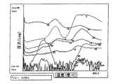
VIII.テスト結果及び測定
実験で、FSG層を有する低k膜を酸素処理を行ったシリコン・ウエハとそれを行わないシリコン・ウエハ上に堆積させた。一部の膜には窒化ケイ素キャップ層を堆積させ、さらに別の膜にはそれを堆積させないで、窒化ケイ素キャップ層の接着特性に対する低圧ストライクの影響を判定した。実験で用いられた膜はCariforinia、Santa ClaraのApplied Materials社によって製造されたUltima(商標名)HDP−CVDチャンバ内で堆積された。チャンバは200mmウエハ用のもので、これもApplied Materials社によって製造されたCentura(登録商標)マルチチャンバ基板処理システム内に配置された。FSG層の平均的なフッ素含有量はWinconsin、MadisonのNicolet Instrument Corporation製造のECO RSシリーズ分光測定装置を用いて%PHRで測定された。それとは別に、Connecticut、NorwalkのPerkin−Elmer Corporationによって製造されたSpectrum 2000 FIR分光測定装置を用いることもできる。SiOピークは通常約1090cm-1と約2005cm-1との間、好ましくは約1097cm-1の波数で起きる。SiFピークは通常約930cm-1と約940cm-1との間、好ましくは約935cm-1の波数で起きる。
【0090】
堆積された膜の安定性は熱堆積分光測定(TDS)によって判定された。サンプルを各ウエハから切り取って、サンプル・チューブ内に入れた。サンプルを含むチューブをTDS器に入れて、真空で加熱して徐々に高温に加熱し、サンプルから放出される種々のガスの濃度を測定した。窒化ケイ素キャップ層を有する膜の安定性をヘイズや泡形成を調べて確認した。膜の接着特性はStudd引っ張りテストで判定した。膜は化学機械的研磨(CMP)の方法でもその安定性と接着力について調べた。TDS測定を行う前の2週間から約2ヶ月間、ウエハを大気条件下で保存した。
【0091】
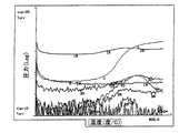
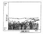
第1及び第2の実験で、FSG層を酸素処理あるいは窒化ケイ素によるキャッピングなしで堆積させた。第1の実験のFSG層は約3.6%PHRのフッ素濃度で堆積された。第1の実験のTDSスペクトルを図7(a)に示す。第2の実験はFSG層は約7.1%PHRのフッ素濃度で堆積された。第2の実験のTDSスペクトルを図7(b)に示す。フッ素濃度は通常のフーリエ変換赤外線(FTIR)測定で判定された。第3の実験のFSG層は上に述べたように酸素処理を伴なう2ステップ・プロセスで堆積された。しかしながら、窒化ケイ素キャップ層をFSG上に堆積させた。第3の実験のTDSスペクトルを図7(c)に示す。第4の実験で、FSG層は上に述べたような酸素処理を伴なう2ステップ・プロセスで堆積され、その後、低圧ストライクを用いて窒化ケイ素でキャップした。第4の実験のTDSスペクトルを図7(d)に示す。
【0092】
次の2つの実験で低圧ストライクを用いて窒化ケイ素でキャップされたFSG膜に対する酸素処理の効果について企画された。これら2つの実験のそれぞれで、TDSサンプルをウエハ・サンプルなしで1000℃に加熱して、サンプル・チューブから脱着されたガスからのバックグランド信号を判定した。第5及び第6の実験で、FSD層が堆積され、上に述べた方法で窒化ケイ素でキャップされた。%PHRで測定したFSG層内のフッ素濃度は第5及び第6の実験で8.0%程度であった。第5の実験の膜は酸素処理なしで堆積された。第5の実験の背景TDSスペクトルを図7(e)に示す。第5の実験のサンプルTDSスペクトルを図7(f)に示す。第6の実験は、第6の実験のFSG膜が窒化ケイ素のキャップ層が上に述べた低圧ストライク法によるFSG層の上部に堆積される前に酸素によって処理された点が第5の実験と異なっていた。第6の実験の背景TDSスペクトルを第7(g)に示す。第5の実験のサンプルTDSスペクトルを図7(h)に示す。
【0093】
図7(a)−(h)に示すグラフ内に示されるTDSスペクトルはウエハ温度の関数としての種々のガスの分圧を示している。図7(a)−(h)で、各ガスを以下の表Iに示すようにその原子質量数で示した。
表I
質量数 ガス
2 水素(H2)
18 水蒸気(H2O)
19 フッ素(F)
20 フッ化水素(HF)
38 フッ素(F2)
40 アルゴン(Ar)
85 トリフルオロシラン(SiF3)
104 テトラフルオロシラン(SiF4)
実験1−6で、ウエハのサンプルを含むサンプル・チューブを約800℃にゆっくり加熱して、脱着されたガスの分圧を質量分光測定を用いて判定した。なお、窒化ケイ素キャップ層がないと、特に質量数20及び19でかなりの量のガス放出が認められる。図7(a)と7(b)に示されている種々のガスのTDSプロットはFSG膜内のフッ素の含有量が大きくなるとガス放出がより激しくなることを示唆している。さらに、ガス放出は温度に非常に強く依存している。なお、ガス放出量と温度依存性の両方が図7(b)にはっきりと示されている。これは第5の実験で堆積されたFSG層内のフッ素含有量がより高いことに依存していると考えられる。図7(c)は酸素処理した膜ではガス放出量がある程度低下していることを示しており、これはFSG膜が窒化ケイ素キャップ層なしでも比較的安定していることを示唆している。なお、図7(c)で、図7(a)及び7(b)と比較して、質量数19、20、38、85及び104のプロットで示されるようにフッ素の放出量がほとんどないことを示唆している。より重要なことは、図7(c)で示されている多少のガス放出が温度に対して非常に弱くしか依存していないことである。図7(d)のTDSプロットは窒化ケイ素層を有している場合はそれがない場合と比較してより安定していることを示唆している。図7(d)に示されているフッ素の放出量は図7(c)の場合と比較してさらに少なくなっている。さらに、多少なりとも行われるガス放出が温度との依存性をほとんど示していない。
【0094】
図7(e)と7(f)は、酸素処理を行わない場合でも、キャップされたFSG膜は500℃の温度までほとんど、あるいはまったくガス放出を行わないことを示唆している。図7(f)は、図7(e)のバックグランド・スペクトルに存在している水蒸気(質量18)は別にして、種々のガスに関する信号はノイズ・レベルとはほとんど区別つかないことを示している。図7(f)の約800℃程度での質量104でのシャープなスパイクは実験の影響を示していると考えられる。同様に、図7(g)と7(h)はガス放出のレベルが酸素で処理された膜と酸素で処理されなかった膜でほとんど同じであることを示している。さらに、図7(g)と7(h)で多少なりともガス放出が起きていても、それは対応するFSG膜上に堆積されている窒化ケイ素キャップの剥離を起こさせるのには不充分であった。
【0095】
これらの膜の接着を熱サイクリングでテストした。各サイクルで、ウエハを窒素雰囲気内で400℃に加熱した。6サイクル後に、ウエハの膜からの剥離について調べた。剥離が観察されない場合、ウエハは合格とされた。何らかの剥離が認められた場合は接着テストで不合格とされた。図7(a)−7(d)の膜に対する接着テストの結果を以下の表IIに要約して示す。
【0096】
これらの結果は、本発明による方法は%PHRで測定して7%以上のフッ素濃度を有する安定した、強力な接着力を示すFSG膜を接着させることができることを示している。さらに、本統合方式では、FSG膜と窒化ケイ素キャップ層の両方を堆積チャンバから基板を取り出さなくてもin situで堆積させることができ、それによって処理量を望むように増大させることが可能になる。そうした膜はプレメタル誘電性(PMD)及び金属間(IMD)アプリケーションにおいても使用することができる。なお、低圧ストライクはHDP−CVDを用いて約1000オングストローム以下の層の堆積に関連した1つの重要な問題も解決してくれる。低圧ストライクによって堆積された薄い層はギャップ充填プロセスにも適用することができる。
【0097】
好ましい実施の形態及び具体例を参照して本発明を上に説明した。当業者であれば別の方式や置き換えも想起できるであろう。従って、添付請求項に示されることを除いて、本発明の限定は意図していない。
【図面の簡単な説明】
【図1A】本発明による高密度プラズマ化学気相堆積システムの1つの実施例を示す簡略図である。
【図1B】図1Aの例示的なCVDプロセスチャンバとともに用いられることができるガス・リングの簡略断面図である。
【図1C】図1Aの例示的なCVDプロセスチャンバとともに用いることができるモニター及びライト・ペンの簡略図である。
【図1D】図1Aの例示的なCVDプロセスチャンバを制御するために用いられる例示的なプロセス制御コンピュータ・プログラム製品のフロー・チャートである。
【図2】本発明による誘電層の実施例を含む例示的な構造を示す断面図である。
【図3】本発明による例示的な低誘電率膜の断面図である。
【図4】本発明による低誘電率膜を堆積させる方法の1つの実施例を示す流れ図である。
【図5】本発明によるキャップ層を堆積させる方法の1つの実施例を示す流れ図である。
【図6】 (a)から(h)は、本発明の1つの実施例による統合されたデュアルダマシンプロセスによって部分的に形成された集積回路の断面図である。
【図7A】低誘電率膜の熱吸収分光図である。
【図7B】低誘電率膜の熱吸収分光図である。
【図7C】低誘電率膜の熱吸収分光図である。
【図7D】低誘電率膜の熱吸収分光図である。
【図7E】低誘電率膜の熱吸収分光図である。
【図7F】低誘電率膜の熱吸収分光図である。
【図7G】低誘電率膜の熱吸収分光図である。
【図7H】低誘電率膜の熱吸収分光図である。[0001]
(Related application)
This application is listed as co-inventors Kasra Khazeni, Michael Cox, Michael Barnes, Huong and Thann Nguyen. Related to patent application entitled Attorney No. AMAT3272). This patent is incorporated herein by reference.
[0002]
(Background of the Invention)
The present invention relates to a method and apparatus for depositing a dielectric layer during a semiconductor substrate manufacturing process. More specifically, the present invention relates to a method for depositing and integrating layers of fluorosilicate glass and silicon nitride in a high density plasma chemical vapor deposition reactor.
[0003]
The size of semiconductor devices tends to decrease consistently, providing more devices and faster devices per manufactured wafer. Since the introduction of semiconductor integrated circuits decades ago, integrated circuits have generally shown a tendency to place a larger number of transistors in a smaller space as device generations change. Currently, a plurality of devices are manufactured with the space between each function kept to 0.25 μm or less. In some examples, the spacing between device functions is 0.18 μm or less. An example of such a feature is a conductive line or trace provided as a pattern on the metal layer. Such traces typically use aluminum. Recently, techniques for depositing traces made of copper have also been developed. Because copper is a more conductive material than aluminum, it is desirable to use copper in these traces.
[0004]
A dielectric non-conductive layer, such as silicon oxide, is often deposited between and above the patterned metal layer. This dielectric layer can provide purposes including insulating conductive features in the layer from each other and protecting the metal layer and / or features from physical or chemical damage. As the spaces or gaps between the conductive features are becoming smaller and smaller, the resulting device capacitance is becoming larger. Increasing capacitance can reduce the processing speed of the integrated circuit. One way to reduce the capacitance is to use a low dielectric constant material. Such materials are often referred to as low-K dielectrics.
[0005]
One way to deposit a dielectric to fill the gap is to incorporate halogen atoms in the silicon dioxide layer. Examples of halogen incorporation are U.S. patent application Ser. Nos. 08 / 548,391, filed Oct. 25, 1995, entitled “Method and Apparatus for Improving Film Stability of Halogen-Doped Silicon Oxide Films”, and 1995. Filed on October 2, 'SiF for depositing more stable F-doped filmsFourUS patent application Ser. No. 08 / 538,696, entitled “Use of”, which is incorporated herein by reference. It is believed that the halogen dopant such as fluorine reduces the dielectric constant of the silicon oxide film because it is an electronegative atom that reduces the polarizability of the overall SiOF network. A silicon oxide film doped with fluorine is sometimes referred to as a fluorosilicate glass (FSG) film.
[0006]
The fluorine content generally determines the properties of the FSG layer, such as the dielectric constant. The fluorine content of FSG is measured as the ratio between two absorption peaks using Fourier Transform Infrared Spectroscopy (FTIR). The height of the first (SiF) peak usually indicates the presence of Si-F bonds. The height of the second (SiO) peak usually indicates the presence of Si-O bonds. The average fluorine concentration in FSG is calculated as follows by percentage peak height ratio (% PHR).
% PHR = SiF / SiO x 100%
Direct measurement of the fluorine content of FSG indicates that the% of PHR is roughly proportional to the% of fluorine atoms in the FSG layer (at.% F). at. % F is
at. % F = (% PHR) x K
Where K is a constant determined empirically. The fluorine concentration (at.% F) can be determined by a method such as secondary ion mass spectrometry (SIMS), attenuated total reflection (ATR), or elemental analysis.
[0007]
One method for depositing the dielectric layer is by gas chemistry. Such a deposition process is called chemical vapor deposition (CVD). The thermal CVD process supplies a reactive gas to the substrate surface where a thermally induced chemical reaction occurs to produce the desired film. The high temperatures at which some thermal CVD processes are performed can damage the metal layers on the device structure. Plasma enhanced CVD (PECVD) processes, on the other hand, excite reactive gases by capacitively coupling radio frequency (RF) energy into a reaction zone near the substrate surface, thereby creating a highly reactive species of plasma. And / or promote dissociation. The high reactivity of the released species reduces the energy required for the chemical reaction to take place, and thus the temperature required for such a CVD process. Unfortunately, some PECVD processes can cause deposition rate variations due to the geometry of the underlying features. These phenomena can create voids in the bottom of the gap.
[0008]
By using a high density plasma CVD (HDP-CVD) system, gap filling can be performed better. In HDP-CVD, the RF coil generates a dielectrically coupled plasma under low pressure conditions. The density of such plasma is about 100 times or more than that of capacitively coupled PECVD plasma. It is believed that the low chamber pressure used in HDP-CVD systems provides a long average migration path for active species. The combination of this long average migration path and high density will allow a significant number of plasma antibiotics to reach the deepest part of the tight gap, resulting in excellent gap filling capability for the membrane. When high density is combined with HDP-CVD, sputtering during deposition is also promoted. This sputtering slows the deposition rate above the gap so that it is not closed too early.
[0009]
Unfortunately, there are several problems associated with the FSG layer isolating copper conductive traces. One problem is that copper exhibits high dispersibility in dielectric materials such as FSG. In addition, poorly formed FSG layers can absorb moisture from reaction products associated with the atmosphere and deposition processes. Copper diffusion and moisture absorption are performed on the FSG or between the FSG layer and the copper layer.ThreeNFour) To deposit a thin layer. Silicon nitride functions as a diffusion barrier. Copper has a diffusion length in the range of 150 to 200 angstroms in silicon nitride. Therefore, Si with a thickness of 200 angstroms or moreThreeNFourIf SiThreeNFourIt is sufficient to prevent copper from diffusing into a dielectric layer extending above or below. Unfortunately, fluorine tends to be released as a gas from FSG at temperatures around 350 ° C. The outgassing fluorine is overlying SiThreeNFourForm “bubbles” in the layer. This bubble is SiThreeNFourMay lead to peeling.
[0010]
One typical approach that has been used to deposit thin films using HDP-CV is to flow argon into the chamber and generate an argon plasma at a pressure of about 40 millitorr. Met. Once the plasma is generated, the pressure in the chamber is reduced to about 5 millitorr (eg, by opening the throttle valve), and deposition gas is introduced into the chamber to deposit the film. Unfortunately, during the first few seconds of this method, for example, the deposition gas does not flow evenly because each gas nozzle is under a different pressure. Deposition begins as soon as the plasma is already on when the deposition gas begins to flow. Therefore, a non-uniform layer with a thickness of several hundreds of angstroms is formed by the first gas explosion caused by the already generated plasma. Film non-uniformity is usually determined by measuring the film thickness at a number of equidistant points (eg 49) and taking the resulting thickness distribution width at half the maximum value. A thin film as described above usually exhibits a non-uniformity on the order of 4.75% within about 10 seconds of plasma generation. This non-uniformity decreases to about 3.5% after about 30 seconds and increases again to about 4% after about 60 seconds.
[0011]
This is generally not a problem for thick films because the initial thickness of the non-uniform layer is usually only a few percent of the total film thickness. For example, for a 10,000 Å thick film, the non-uniform initial layer thickness is 300 Å. This non-uniform initial layer is only 3 percent of the total film thickness. However, in the case of a film having a thickness of 1000 angstroms or less, the same 300 angstrom non-uniform layer occupies 30% or more of the total film thickness. Such non-uniformities are often undesirable in the cap layer.
[0012]
Accordingly, there is a need in the art for a stable low dielectric constant FSG film having a silicon nitride cap layer that is highly adherent at high temperatures and a method for depositing it.
[0013]
(Summary of Invention)
The method according to the invention is based on the prior art by depositing a silicon oxide layer (for example FSG) on a substrate and treating the dielectric layer with oxygen before forming a silicon nitride cap on the layer. Overcoming the deficiencies in Oxygen treatment stabilizes FSG. In one embodiment of the present invention, an FSG layer with a fluorine content of greater than about 7% as measured by peak height ratio is deposited by HDP-CVD and processed by oxygen plasma. A thin (<1000 angstrom) layer of silicon nitride is deposited on the layer of FSG using a low pressure strike as described in sufficient detail below.
[0014]
The first dielectric is a silicon-containing gas, a fluorine-containing gas, and an oxygen-containing gas that is flowed into the deposition chamber to generate a first plasma and use the first plasma to deposit a first dielectric layer. Can be deposited. The second dielectric layer may be deposited by flowing one or more process gases into the deposition chamber, performing a low pressure strike, and starting deposition of the second dielectric in the second strike. it can. Low pressure strikes can be achieved by establishing the process gas flow so that the pressure in the chamber is between 5 and 10 mTorr and turning on the bias voltage for a time sufficient to establish a weak plasma. Weak plasma can be capacitively coupled. When the weak plasma is coupled, the source voltage is turned on and then the bias voltage is turned off.
[0015]
Alternatively, the low dielectric constant film deposits fluorosilicate glass (FSG) having a first atomic ratio of fluorine to oxygen and treats the FSG to reduce the ratio of fluorine to oxygen before the FSG layer. It can be formed by depositing silicon nitride thereon. Preferably, FSG deposition, oxygen treatment, and silicon nitride deposition are all performed in the same chamber without removing the substrate from the chamber.
[0016]
In another embodiment, the low dielectric constant film is formed with a FSG layer between two layers of silicon nitride. Each silicon nitride layer is formed using a low pressure strike, and the FSG layer is treated with oxygen to enhance the stability of the film.
[0017]
Various versions of the present invention can be implemented as program code for controlling a semiconductor wafer processing system. The program code can be stored in a suitable computer readable storage medium. The program code comprises a deposition chamber, a gas panel coupled to the chamber, a plasma generator coupled to the chamber, and a controller coupled to the gas panel, a source power source and a bias power source. It can be configured to control the deposition apparatus. The controller typically includes a computer readable medium having the program code.
[0018]
Films deposited according to various embodiments according to the present invention have a low dielectric constant, good thermal stability, and strong adhesion. Furthermore, the integrity of the process can be enhanced by depositing both films by in situ HDP-CVD. These embodiments of the present invention are particularly useful in copper damascene applications.
[0019]
(Description of Examples)
I. Introduction
An embodiment of the method according to the invention is to deposit a stable multilayer dielectric film having a low dielectric constant. This film is stabilized by oxygen and covered with a uniform layer of silicon nitride having a thickness of less than 1000 angstroms. In a special embodiment of the method according to the invention, the fluorine content of the fluorosilicate glass (FSG) is measured in% PHR by Fourier transform infrared spectroscopy (FTIR). SiF peak is usually about 890cm-1The SiO peak is usually about 1040-1100 cm.-1Is the wave number. The fluorine concentration in the FSG is measured as a percentage peak height ratio (% PHR) as described above. In certain embodiments, the FSG layer has a fluorine content of about 7% or more as measured by% PHR.
[0020]
Low pressure strikes provide high uniformity in the thin layer by stabilizing the desired gas flow before generating the plasma. Both layers are deposited in situ using HDP-CVD, which allows process integration.
[0021]
II. Exemplary substrate processing system
FIG. 1A illustrates one embodiment of a high density plasma chemical vapor deposition (HDV-CVD)
[0022]
The upper portion of the
[0023]
A
[0024]
The lower portion of the
[0025]
The
[0026]
Source plasma system 80A includes a
[0027]
The bias plasma system 80B includes a bias RF (BRF) generator 31C and a bias matching network 32C. The bias plasma system 80B is capacitively coupled to
This bias plasma system 80B contributes to the enhanced transfer of plasma species (eg, ions) produced by the source plasma system 80A to the substrate surface. In a special embodiment, the bias RF generator provides up to 5,000 watts of RF power at 13.56 MHz.
[0028]
[0029]
[0030]
Other means also help stabilize the plasma. For example, the RF control circuit can be used to determine the power applied to the load (plasma), and the generator output power supply can be increased or decreased to substantially constant the power transmitted during the deposition of one layer. You can also.
[0031]
The
[0032]
In one embodiment, the first and
[0033]
The
[0034]
In embodiments where flammable, toxic, or corrosive gases are used, it is desirable to remove the gas remaining in the gas transmission line after deposition. This can be accomplished using a three-way valve, such as valve 43B, to disconnect
[0035]
In FIG. 1A, the
[0036]
A remote ultra high frequency
[0037]
[0038]
FIG. 1C shows a portion of a specific system user interface used in conjunction with the CVD processing chamber shown as an example in FIG. 1A.
[0039]
The
[0040]
The computer program code can be written in any conventional computer readable language such as 68000 assembly language, C, C ++, Pascal.
Appropriate program code is placed in a file or files using a conventional text editor and stored on a computer-usable medium such as the computer's memory system. If the entered code text is written in a high-level language, the code is compiled and the resulting computer code is then combined with the precompiled window library routine object code . To execute the combined compiled object code, when the system user invokes the object code, the computer system loads the code into storage, from which the CPU is in the program. Read and execute the code to perform the tasks identified in.
[0041]
1D is a configuration diagram showing a hierarchical control structure of a
The
[0042]
Signals for monitoring the process are provided by the analog input and digital input board of the system controller, and signals for controlling the process are output on the analog output and digital output board of the
[0043]
The
[0044]
Once the
[0045]
Examples of chamber component subroutines are
[0046]
The operation of a particular chamber component subroutine is described below with reference to FIG. 1D.
[0047]
The
[0048]
Typically, the process
[0049]
In some processes, before a reactive process gas is introduced into the chamber, an inert gas such as argon is introduced into the chamber to stabilize the pressure in the chamber. For these processes, the process
[0050]
In addition, if it is necessary to evaporate the process gas from a liquid precursor, such as tetraethyloxysilane (TEOS), the process
[0051]
In addition, the process
[0052]
The process
[0053]
The
[0054]
The chamber pressure can be measured by, for example, a manometer, and the position of the throttle valve 26 can be adjusted according to the
[0055]
When the
[0056]
The
[0057]
The chamber or substrate temperature can also be measured with a thermocouple or pyrometer, and the temperature is controlled by a separate temperature controller. Such temperature controllers include heater elements, cooling elements, or both. Such heating / cooling elements can be coupled to the
[0058]
When the
[0059]
The
[0060]
An example of a system that incorporates some or all of the subsystems and routines described above would be an Ultima System manufactured by Applied Materials that is configured to implement the present invention. Details of these systems are co-inventors, Fred C. Redeker, Farhad Moghadam, HIrogi Hanakawa, Tetsuya Ishikawa, Dan Maydan, Shijian Li, Brian Lue, Robert Steger, Yaxin Wang, Manus Wong, and Ashok Sinha as co-inventors. Listed and disclosed in US patent application Ser. No. 08 / 679,927 entitled “Symmetrically Adjustable Inductively Coupled HDP-CVD Reactor” filed July 15, 1996, the disclosure of which Are incorporated herein by reference.
[0061]
III. Example structure
FIG. 2 shows a simplified cross-sectional view of an
[0062]
The premetal dielectric layer 221 separates the
The
[0063]
Preferably, at least one of the gap-fill layers 227b, 228b, 229b, and 230b includes FSG treated with oxygen in accordance with the first embodiment of the present invention.
More preferably, at least one of the cap layers 227c, 228c, 229c and 230c is deposited using a low pressure strike according to the second embodiment of the present invention. Most preferably, the cap layer according to the second embodiment is deposited on the gap-fill layer treated with oxygen according to the first embodiment.
[0064]
The layers according to the present invention could be utilized in each of the dielectric layers shown in
[0065]
Note that the simplified integrated circuit 100 is for illustrative purposes only. Those skilled in the art will be able to apply the invention to the manufacture of other integrated circuits such as microprocessors, application specific integrated circuits (ASICs), storage devices and the like.
[0066]
IV. Exemplary low dielectric constant film
Dielectric films deposited in accordance with embodiments of the present invention generally have a low dielectric constant. The low dielectric constant means here that it is lower than the dielectric constant of the undoped silicon oxide film. In general, silicon oxide (SixOy) Has a dielectric constant k of about 4. A film whose k is 4 or more is called a high-k film. The low dielectric constant is provided by fluorine atoms incorporated into the silicon oxide layer of the film to form a layer of fluorosilicate glass (FSG). Such a dielectric film can be used as an intermetal dielectric (IMD) film or other type of dielectric layer. The following specific example shows an IMD layer formed on a copper trace, which together has a thickness of 0.25 microns and an aspect ratio of 4: 1. This film has a thin silicon nitride layer, which adheres strongly to the FSG. The silicon nitride layer functions as a dispersion barrier between the copper and the FSG layer. Therefore, this layer not only has a low dielectric constant, but also has an excellent gap filling property, and is excellent in coexistence with a copper structure preliminarily existing on a semiconductor substrate.
[0067]
FIG. 3 is a simplified cross-sectional view of one embodiment of the present invention having a two-layer
[0068]
V. Low dielectric constant film deposition
FIG. 4 is a flow chart of one embodiment of a deposition method according to the present invention in which oxygen treatment enhances the stability of the FSG layer. In this embodiment, the process is performed in a single process chamber, but the process can be applied to a multi-chamber system or can be performed in a series of different chambers and systems. Similarly, the process parameters described below are for an 8-inch process wafer, but the process can be modified to accommodate other wafers, such as a 10-inch wafer.
[0069]
The wafer is placed on a substrate support member in the processing chamber through a vacuum lock door or slit valve (step 402) and moved to a desired processing position. A process gas comprising a silicon source, a fluorine source, and an oxygen source is introduced into the chamber and a high density plasma is formed to deposit a layer of FSG (step 404) on the wafer. In a preferred embodiment, the silicon source is monosilane (SiHFourTetrafluorosilane (SiF), which is considered to be a silicon source.Four) And the oxygen source is diatomic oxygen (O2). TEOS or disilane (Si2H6), Trisilane (SiThreeH8), Tetrasilane (SiFourHTenOther silanes such as) can also be used as a silicon source. Similarly, F2Other gases such as can also be used as the fluorine source. Ozone (OThree) Can be used as another oxygen source. The plasma can optionally contain an inert gas such as helium or argon. Generally, it is easier to generate plasma in argon than helium. Other inert gases such as neon, krypton, or xenon can be used, but krypton and xenon tend to be more expensive than helium and argon.
[0070]
These gases are SiFFourFor SiH, with flow rates in the range of 90 and 94 standard cubic centimeters (Sccm) per minuteFourIn the case of 50-54sccm, and O2Is provided at a flow rate in the range of 155-165 sccm. The gas flow rate is more preferably SiFFourAbout 94 standard cubic centimeters per minute (sccm), SiHFourIn the case of 50sccm, then O2In this case, it is 160 sccm. The pressure in the chamber is usually set and maintained in the range of about 3.5-6 mTorr, preferably about 4 mTorr. The plasma can be formed by the application of single or mixed frequency RF power. Generally, the
[0071]
The above process conditions are maintained for a time sufficient to form an FSG layer having a thickness of about 6,000 angstroms to 12,000 angstroms, preferably about 8,000-10,000 angstroms. The actual deposition time depends on the chamber used. As an example, for the example chamber shown in FIGS. 1a through 1d, an FSG layer 8000 angstroms thick can be deposited in about 90 seconds using the above parameters. At this stage, the FSG film deposited under the above conditions has a relatively high fluorine to oxygen atomic ratio. In a preferred embodiment, the FSG layer has a fluorine concentration in the range of about 7.8% to about 8.0% as measured by% PHR prior to treating the FSG layer with oxygen. In general, O2The / Si ratio is in the range of about 1.0-1.2, preferably about 1.1. This O2/ Si ratio is O, as shown below2, SiFFourAnd SiHFourDepends on the flow rate.
O2/ Si = O2(SiFFour + SiHFour)
Usually SiFFour/ SiHFourThe flow rate ratio ranges from about 1.7 to about 1.8, preferably about 1.75. The actual flow rate depends on the chamber used.
[0072]
The dielectric constant k and refractive index n of the FSG layer depend on the atomic ratio (percent) of fluorine in the FSG film. Usually, the larger the sulfur content, the smaller the values of k and n. An FSG film having a fluorine content of about 0 at% and an undoped silicate glass (USG) usually have a k value of about 4 and a refractive index of about 1.46. If the FSG film is doped to about 10at% with fluorine, the refractive index will be in the range of 3.4-3.7, andRefractive indexThe range is 1.40–1.43. The dielectric constant of the film is usually determined by a reference film with a known capacitance and voltage (C-V) measurement and k value of the deposited film.
[0073]
In addition to the methods described above for depositing FSG, several different processes are known for forming fluorinated silicon glass (FSG). One such process uses triethoxyfluorosilane (TEFS) with tetraethyloxysilane (TEOS) in a PECVD deposition process. Yet another process for forming FSG films is C as the fluorine source in the PECVD process.2F6Is used. Such an FSG deposition process is described in US patent application Ser. No. 09 / 075,592, assigned to Applied Materials.
[0074]
After forming the FSG layer, the surface of the FSG layer is treated with oxygen to reduce the fluorine to oxygen ratio (step 406). Oxygen treatment can be achieved, for example, by heating the FSG layer during exposure to oxygen or ozone, or irradiating with active oxygen ions or active neutral oxygen atoms. In one preferred embodiment, the FSG layer is irradiated with oxygen ions from the plasma in the same chamber in which the FSG is deposited. Usually SiFFourAnd SiHFourThe flow is stopped at the end of the FSG deposition, while the oxygen flow rate is maintained at approximately the same level as in step 404. The plasma is maintained using approximately the same power and frequency settings for the source RF that was used during deposition. The bias RF frequency usually remains the same during oxygen treatment, as during FSG deposition, but the BRF power is increased by a third from the value used during deposition. In a more preferred embodiment, the BRF power is maintained in the 1500 W-1800 W range during oxygen treatment.
[0075]
During the oxygen process, the wafer temperature is maintained at about 420 ° C. The chamber pressure is maintained at about 1.8-2.5 mTorr, preferably about 2 mTorr, for about 10 seconds to 1 minute, preferably about 20 seconds. A high wafer throughput through the processing system is desirable, and therefore the processing time should be as short as possible while performing sufficient oxygen processing. The exact time required depends on many factors, including how the previous HDP-CVD was performed. Oxygen enters the FSG layer where it reacts with fluorine to make the resulting film more stable. The FSG layer has a fluorine concentration in the range of about 7.5% to about 7.8% after treatment with oxygen, as measured by% PHR.
[0076]
Optionally, a silicon nitride cap layer may be deposited on the FSG layer (step 408). This capping layer is not necessary to achieve the lower dielectric constant of the underlying layer, but makes the FSG layer more compatible with the subsequent integrated circuit processing steps. The FSG layer can be planarized or densified before the cap layer is formed. The cap layer can be formed using an HDP-CVD process similar to the process described above. However, in order to control the deposition of a very thin film, for example, a thickness of 1000 Angstroms or less, a special low pressure strike is required to initiate the plasma.
[0077]
VI. Cap layer deposition using low pressure strikes.
It is preferred to deposit a thin cap layer of silicon nitride on the FSG film. In damascene applications, silicon nitride deposited on copper serves as a barrier to copper diffusion into the upper or lower layer. Silicon nitride deposited on a dielectric layer such as FSG also serves as an etching step. Since silicon nitride is 3.4 for FSG containing about 10% atomic%, the k value is about 7, so a thin layer of silicon nitride is desirable. The effective dielectric constant of the composite dielectric layer depends on the thickness and dielectric constant of each layer constituting the film.
Generally, the dielectric constant is K1And K2, And each thickness is d1And d2In the case of a film composed of two layers, the effective dielectric constant K of the filmeffDepends on the dielectric constant and thickness of each layer. Usually, the thinner layer has a greater effect on the effective dielectric constant of the film. Thus, silicon nitride has a much higher dielectric constant than FSG, but if the silicon nitride layer is sufficiently thin compared to the overall film thickness, the effective dielectric constant of the film will approach that of FSG. be able to.
[0078]
In addition to being thin, silicon nitride usually must be uniform. In order to deposit a uniform thin silicon nitride layer after FSG deposition, it is often desirable to ignite the plasma while flowing the deposition gas. FIG. 5 is a flow diagram of one embodiment of a method for depositing a cap layer according to the present invention using a low pressure strike. US Patent Application entitled “Low Pressure Strike in HDP-CVD Chamber”, patent application number AMAT / 3272 / PDD / KPU3, filed concurrently with the present application, incorporated herein by reference and co-assigned. / Fully described by JW. The method embodiment shown in FIG. 5 is the preferred embodiment of
[0079]
The substrate temperature is established at step 506. Silicon nitride (SixNyIn general, a substrate temperature of about 430 ° C. is established before deposition. For example, only an inert plasma may be used to heat the substrate to establish the substrate, such as exposing the substrate to plasma. The exposure time depends on the temperature rise required for the substrate. Usually, the hotter the substrate, the shorter the time for heating it. In order to increase throughput, it is generally preferred to deposit the cap layer as soon as possible after the lower layer has been deposited, that is, if the wafer is already hot. For example, if the cap layer must be deposited immediately after FSG deposition, the substrate is already quite hot. In such situations, exposing the substrate to an inert plasma for about 10 seconds is usually sufficient to heat the substrate to the desired temperature for cap layer deposition. Also, the heating elements in the substrate support can be used to heat the substrate alone or in combination with plasma. Once the desired temperature for deposition has been established, the source RF is turned off at step 508 with the inert gas still flowing. Without the source RF, there is no plasma in the chamber. At the moment when the source RF is turned off, the deposition gas is introduced into the chamber and mixed with the inert gas. SixNyIn the case of a cap layer, the deposition gas typically includes a silicon source and a nitrogen source. In one preferred embodiment, the silicon source is SiHFourAnd the nitrogen source is diatomic nitrogen (N2). Si2H6Other organosilanes can be used as silicon source, such as ammonia (NHThreeOther nitrogen-containing gases such as) can be used as the nitrogen source.
[0080]
At
[0081]
Steps 502 to 508 are optional. These steps are used in special cases where a low pressure strike is used to deposit the cap layer in situ immediately after the deposition of the lower layer in the same chamber. Also, the low pressure strike method can be started simultaneously with stabilization of gas flow rate and chamber pressure as in
[0082]
Once the flow rate and chamber pressure are established, a weak plasma is established in the chamber at step 512. Typically, for pressures less than about 40 millitorr, it is easier to establish a capacitively coupled plasma than an inductively coupled plasma.
When a weak plasma is established, the source RF is turned on and a deposition plasma is established at step 514. The expression weak plasma means that the plasma power is low enough to avoid damage to the device formed on the substrate. Such a weak, capacitively coupled plasma can be established by applying a direct current (DC) or RF bias to the
[0083]
Once a weak plasma is established, the source RF is turned on, a deposition plasma is established at step 514, and the substrate bias is turned off as soon as the source RF is turned on. If the substrate bias is turned off before the source RF is turned on, the plasma usually disappears, which is undesirable. Therefore, there is some overlap in the period when both the source RF and the bias RF are normally turned on. Usually, this overlap period corresponds to almost the second half of the bias period. For example, when the substrate bias is turned on for a bias period of 0.5 to 1.0 seconds, the source RF is turned on for a period that overlaps the last 0.25 to 0.5 seconds when the substrate bias is turned on. Usually, it is desirable to make the bias period and the overlap period as short as possible. The lower limit of the bias period and overlap period usually depends on the response speed of the generator and the electronic characteristics of the substrate bias and source RF signal.
[0084]
The cap layer is deposited at
[0085]
While one embodiment of the method according to the present invention has been described above with reference to an example of depositing a silicon nitride cap layer on an FSG layer, other and further books may be used without departing from the basic scope thereof. It is possible to devise embodiments of the invention. For example, the FSG deposition step and the silicon nitride deposition step can be reversed. That is, a thin (<1000 Å) silicon nitride layer is deposited on the substrate using a low pressure strike as described above with reference to FIG. 5 and a layer of FSG or other material is deposited, eg, HDP-CVD. It would be possible to deposit on silicon nitride using Silicon nitride functions as a barrier layer between the FSG and the underlying layer. It would also be possible to deposit another thin silicon nitride layer in the FSG layer as a cap layer using a second low pressure strike. Thus, FSG can be “sandwiched” between two thin layers of silicon nitride to prevent the FSG from peeling from the underlying substrate, while preventing other layers on the FSG from peeling. Such a “sandwich” structure is desirable, for example, for damascene applications.
[0086]
VII. Exemplary damascene process
An example of the copper damascene process integration method using the dielectric film as described above is shown in FIGS. 6 (a) -6 (b). The dual damascene process is initiated by depositing an
[0087]
After planarization of the copper layer 614, a barrier layer 616, such as silicon nitride, a second FSG layer 618, a second etch stop layer, and a
[0088]
The damascene process is used in equipment that uses copper interconnects because an acceptable method for etching copper is not currently available. This is because structures composed of damascene processes do not require gap-filling dielectrics and typically exhibit lower RC collapse compared to similar structures formed using aluminum metal lines. Furthermore, faster deposition rates can be used in the damascene process since gap filling is not a problem. Although the etch stop and barrier layers are described as silicon nitride, other materials may be deposited using low pressure strike deposition as described above with reference to FIGS. 3-5.
[0089]
VIII. Test results and measurements
In experiments, low-k films with FSG layers were deposited on silicon wafers with and without oxygen treatment. The silicon nitride cap layer was deposited on some films and not on other films to determine the impact of low pressure strikes on the adhesion properties of the silicon nitride cap layer. The films used in the experiments were deposited in an Ultima ™ HDP-CVD chamber manufactured by Applied Materials, Califorinia, Santa Clara. The chamber was for a 200 mm wafer and was also placed in a Centura® multi-chamber substrate processing system manufactured by Applied Materials. The average fluorine content of the FSG layer was measured at% PHR using an ECO RS series spectrometer manufactured by Nicolet Instrument Corporation of Winconsin, Madison. Alternatively, a Spectrum 2000 FIR spectrometer manufactured by Perkin-Elmer Corporation of Connecticut, Norwalk can be used. SiO peak is usually about 1090cm-1And about 2005cm-1Between, preferably about 1097cm-1It happens at the wave number of. SiF peak is usually about 930cm-1And about 940cm-1Between, preferably about 935cm-1It happens at the wave number of.
[0090]
The stability of the deposited film was determined by thermal deposition spectroscopy (TDS). Samples were cut from each wafer and placed in sample tubes. The tube containing the sample was placed in a TDS apparatus, heated in vacuum and gradually heated to a high temperature, and the concentrations of various gases released from the sample were measured. The stability of the film having the silicon nitride cap layer was confirmed by examining haze and bubble formation. The adhesive properties of the film were determined by the Studd tensile test. The film was also investigated for its stability and adhesion by chemical mechanical polishing (CMP). The wafers were stored under atmospheric conditions for about 2 months from 2 weeks before TDS measurement.
[0091]
In the first and second experiments, the FSG layer was deposited without oxygen treatment or capping with silicon nitride. The first experimental FSG layer was deposited at a fluorine concentration of about 3.6% PHR. The TDS spectrum of the first experiment is shown in FIG. In the second experiment, the FSG layer was deposited at a fluorine concentration of about 7.1% PHR. The TDS spectrum of the second experiment is shown in FIG. The fluorine concentration was determined by ordinary Fourier transform infrared (FTIR) measurement. The FSG layer of the third experiment was deposited in a two-step process with oxygen treatment as described above. However, a silicon nitride cap layer was deposited on the FSG. The TDS spectrum of the third experiment is shown in FIG. In a fourth experiment, the FSG layer was deposited in a two-step process with oxygen treatment as described above and then capped with silicon nitride using a low pressure strike. The TDS spectrum of the fourth experiment is shown in FIG.
[0092]
In the next two experiments, the effect of oxygen treatment on the FSG film capped with silicon nitride using a low pressure strike was planned. In each of these two experiments, a TDS sample was heated to 1000 ° C. without a wafer sample and the background signal from the gas desorbed from the sample tube was determined. In the fifth and sixth experiments, an FSD layer was deposited and capped with silicon nitride in the manner described above. The fluorine concentration in the FSG layer measured by% PHR was about 8.0% in the fifth and sixth experiments. The film of the fifth experiment was deposited without oxygen treatment. The background TDS spectrum of the fifth experiment is shown in FIG. A sample TDS spectrum of the fifth experiment is shown in FIG. The sixth experiment differs from the fifth experiment in that the FSG film of the sixth experiment was treated with oxygen before the silicon nitride cap layer was deposited on top of the FSG layer by the low pressure strike method described above. It was different. The background TDS spectrum of the sixth experiment is shown in FIG. 7 (g). A sample TDS spectrum of the fifth experiment is shown in FIG.
[0093]
The TDS spectra shown in the graphs shown in FIGS. 7 (a)-(h) show the partial pressures of various gases as a function of wafer temperature. 7A to 7H, each gas is shown by its atomic mass number as shown in Table I below.
Table I
Mass number Gas
2 Hydrogen (H2)
18 Water vapor (H2O)
19 Fluorine (F)
20 Hydrogen fluoride (HF)
38 Fluorine (F2)
40 Argon (Ar)
85 Trifluorosilane (SiFThree)
104 Tetrafluorosilane (SiFFour)
In Experiment 1-6, the sample tube containing the wafer sample was slowly heated to about 800 ° C., and the partial pressure of the desorbed gas was determined using mass spectrometry. In the absence of a silicon nitride cap layer, a significant amount of outgassing is observed, especially at mass numbers of 20 and 19. The TDS plots for various gases shown in FIGS. 7 (a) and 7 (b) suggest that the outgassing becomes more intense as the fluorine content in the FSG film increases. Furthermore, outgassing is very strongly dependent on temperature. Note that both the gas release amount and the temperature dependence are clearly shown in FIG. This is believed to depend on the higher fluorine content in the FSG layer deposited in the fifth experiment. FIG. 7 (c) shows that the amount of outgassing is reduced to some extent in the oxygen-treated film, which suggests that the FSG film is relatively stable without the silicon nitride cap layer. In FIG. 7 (c), compared with FIGS. 7 (a) and 7 (b), there is almost no release of fluorine as shown by plots of
[0094]
FIGS. 7 (e) and 7 (f) suggest that the capped FSG film emits little or no gas up to a temperature of 500 ° C. even without oxygen treatment. FIG. 7 (f) shows that apart from water vapor (mass 18) present in the background spectrum of FIG. 7 (e), signals for various gases are almost indistinguishable from noise levels. ing. The sharp spike at
[0095]
The adhesion of these membranes was tested by thermal cycling. In each cycle, the wafer was heated to 400 ° C. in a nitrogen atmosphere. After 6 cycles, peeling of the wafer from the film was examined. If no delamination was observed, the wafer was accepted. If any peeling was observed, the adhesion test was rejected. The results of adhesion tests on the films of FIGS. 7 (a) -7 (d) are summarized in Table II below.
[0096]
These results show that the method according to the present invention can adhere a stable and strong FSG film with a fluorine concentration of 7% or more as measured by% PHR. In addition, the integrated scheme allows both FSG films and silicon nitride cap layers to be deposited in situ without removing the substrate from the deposition chamber, thereby allowing throughput to be increased as desired. . Such films can also be used in premetal dielectric (PMD) and intermetal (IMD) applications. Low pressure strikes also solve one important problem associated with the deposition of layers below about 1000 angstroms using HDP-CVD. Thin layers deposited by low pressure strike can also be applied to the gap filling process.
[0097]
The invention has been described above with reference to preferred embodiments and specific examples. Those skilled in the art will be able to recall other schemes and substitutions. Accordingly, no limitation on the invention is intended except as indicated in the appended claims.
[Brief description of the drawings]
FIG. 1A is a simplified diagram illustrating one embodiment of a high density plasma chemical vapor deposition system in accordance with the present invention.
FIG. 1B is a simplified cross-sectional view of a gas ring that can be used with the exemplary CVD process chamber of FIG. 1A.
1C is a simplified diagram of a monitor and light pen that can be used with the exemplary CVD process chamber of FIG. 1A.
1D is a flow chart of an exemplary process control computer program product used to control the exemplary CVD process chamber of FIG. 1A.
FIG. 2 is a cross-sectional view illustrating an exemplary structure including an embodiment of a dielectric layer according to the present invention.
FIG. 3 is a cross-sectional view of an exemplary low dielectric constant film according to the present invention.
FIG. 4 is a flow diagram illustrating one embodiment of a method for depositing a low dielectric constant film according to the present invention.
FIG. 5 is a flow diagram illustrating one embodiment of a method for depositing a cap layer according to the present invention.
6 (a) to (h) are cross-sectional views of an integrated circuit partially formed by an integrated dual damascene process according to one embodiment of the present invention.
FIG. 7A is a heat absorption spectroscopic diagram of a low dielectric constant film.
FIG. 7B is a heat absorption spectroscopic diagram of a low dielectric constant film.
FIG. 7C is a heat absorption spectroscopic diagram of a low dielectric constant film.
FIG. 7D is a heat absorption spectroscopic diagram of a low dielectric constant film.
FIG. 7E is a heat absorption spectroscopic diagram of a low dielectric constant film.
FIG. 7F is a heat absorption spectroscopic diagram of a low dielectric constant film.
FIG. 7G is a heat absorption spectroscopic diagram of a low dielectric constant film.
FIG. 7H is a heat absorption spectroscopic diagram of a low dielectric constant film.
Claims (14)
Translated fromJapanese上記基板上にフルオロケイ酸塩ガラス(FSG)層を堆積させるステップと、
前記FSG層を堆積した後に、酸素をフッ素と反応させて前記FSG層における酸素原子に対するフッ素原子の比率を低下させることにより前記FSG層を安定化させるように前記FSG層を酸素に露出させるステップと、
その後、前記FSG層上に窒化ケイ素層を堆積させるステップと
を含む、方法。A method of depositing a multilayer dielectric film on a substrate, comprising:
Depositing a fluorosilicate glass (FSG) layer on the substrate;
After depositing the FSG layer, exposing the FSG layer to oxygen to stabilize the FSG layer by reacting oxygen with fluorine to reduce the ratio of fluorine atoms to oxygen atoms in the FSG layer; ,
And thereafter depositing a silicon nitride layer on the FSG layer.
上記基板上に、フッ素原子:酸素原子の第1の原子比率でフルオロケイ酸塩ガラス(FSG)を堆積させるステップと、
前記FSG層を堆積した後に、酸素をフッ素と反応させて前記FSG層における酸素原子に対するフッ素原子の比率を低下させることにより前記FSG層を安定化させるように前記FSG層を酸素に露出させるステップと、
その後、前記FSG層の上部に窒化ケイ素層を堆積させるステップと
を含み、
前記FSG堆積、酸素への露出、及び窒化ケイ素堆積がすべて1つのチャンバ内で行われ、基板が前記チャンバから取り出されない、方法。A method of depositing a dielectric film on a substrate, comprising:
Depositing fluorosilicate glass (FSG) on the substrate at a first atomic ratio of fluorine atoms: oxygen atoms;
After depositing the FSG layer, exposing the FSG layer to oxygen to stabilize the FSG layer by reacting oxygen with fluorine to reduce the ratio of fluorine atoms to oxygen atoms in the FSG layer; ,
Then depositing a silicon nitride layer on top of the FSG layer;
The method, wherein the FSG deposition, exposure to oxygen, and silicon nitride deposition are all performed in one chamber and the substrate is not removed from the chamber.
Applications Claiming Priority (2)
| Application Number | Priority Date | Filing Date | Title |
|---|---|---|---|
| US09/470,561US6372291B1 (en) | 1999-12-23 | 1999-12-23 | In situ deposition and integration of silicon nitride in a high density plasma reactor |
| US09/470561 | 1999-12-23 |
Publications (2)
| Publication Number | Publication Date |
|---|---|
| JP2001267315A JP2001267315A (en) | 2001-09-28 |
| JP4721510B2true JP4721510B2 (en) | 2011-07-13 |
Family
ID=23868100
Family Applications (1)
| Application Number | Title | Priority Date | Filing Date |
|---|---|---|---|
| JP2000392852AExpired - Fee RelatedJP4721510B2 (en) | 1999-12-23 | 2000-12-25 | Method for depositing a multilayer dielectric film on a substrate |
Country Status (6)
| Country | Link |
|---|---|
| US (1) | US6372291B1 (en) |
| EP (1) | EP1111664A3 (en) |
| JP (1) | JP4721510B2 (en) |
| KR (1) | KR100726517B1 (en) |
| SG (1) | SG93911A1 (en) |
| TW (1) | TW518693B (en) |
Families Citing this family (78)
| Publication number | Priority date | Publication date | Assignee | Title |
|---|---|---|---|---|
| US6200911B1 (en)* | 1998-04-21 | 2001-03-13 | Applied Materials, Inc. | Method and apparatus for modifying the profile of narrow, high-aspect-ratio gaps using differential plasma power |
| US6255233B1 (en)* | 1998-12-30 | 2001-07-03 | Intel Corporation | In-situ silicon nitride and silicon based oxide deposition with graded interface for damascene application |
| FR2795746B1 (en)* | 1999-07-01 | 2001-07-27 | Commissariat Energie Atomique | METHOD FOR DEPOSITING SILICON-BASED DIELECTRIC MATERIAL ON COPPER |
| US6468927B1 (en)* | 2000-05-19 | 2002-10-22 | Applied Materials, Inc. | Method of depositing a nitrogen-doped FSG layer |
| TW584902B (en)* | 2000-06-19 | 2004-04-21 | Applied Materials Inc | Method of plasma processing silicon nitride using argon, nitrogen and silane gases |
| US6846737B1 (en)* | 2000-08-15 | 2005-01-25 | Intel Corporation | Plasma induced depletion of fluorine from surfaces of fluorinated low-k dielectric materials |
| US6534357B1 (en)* | 2000-11-09 | 2003-03-18 | Micron Technology, Inc. | Methods for forming conductive structures and structures regarding same |
| US6740601B2 (en)* | 2001-05-11 | 2004-05-25 | Applied Materials Inc. | HDP-CVD deposition process for filling high aspect ratio gaps |
| US6596653B2 (en)* | 2001-05-11 | 2003-07-22 | Applied Materials, Inc. | Hydrogen assisted undoped silicon oxide deposition process for HDP-CVD |
| US6879046B2 (en)* | 2001-06-28 | 2005-04-12 | Agere Systems Inc. | Split barrier layer including nitrogen-containing portion and oxygen-containing portion |
| US6531412B2 (en)* | 2001-08-10 | 2003-03-11 | International Business Machines Corporation | Method for low temperature chemical vapor deposition of low-k films using selected cyclosiloxane and ozone gases for semiconductor applications |
| JP4090766B2 (en)* | 2002-03-19 | 2008-05-28 | 富士通株式会社 | Manufacturing method of semiconductor device |
| WO2003098678A1 (en)* | 2002-05-16 | 2003-11-27 | Tokyo Electron Limited | Method of treating substrate |
| JP3504940B2 (en)* | 2002-05-17 | 2004-03-08 | 沖電気工業株式会社 | Method for manufacturing semiconductor device |
| DE10229463B4 (en)* | 2002-07-01 | 2008-12-11 | Qimonda Ag | Semiconductor device and method for its production |
| US6934032B1 (en)* | 2002-09-30 | 2005-08-23 | Advanced Micro Devices, Inc. | Copper oxide monitoring by scatterometry/ellipsometry during nitride or BLOK removal in damascene process |
| EP1408140A1 (en)* | 2002-10-11 | 2004-04-14 | STMicroelectronics S.r.l. | A high-density plasma process for depositing a layer of Silicon Nitride |
| US6833322B2 (en)* | 2002-10-17 | 2004-12-21 | Applied Materials, Inc. | Apparatuses and methods for depositing an oxide film |
| US20040121146A1 (en)* | 2002-12-20 | 2004-06-24 | Xiao-Ming He | Composite barrier films and method |
| US6808748B2 (en)* | 2003-01-23 | 2004-10-26 | Applied Materials, Inc. | Hydrogen assisted HDP-CVD deposition process for aggressive gap-fill technology |
| DE10311312B4 (en)* | 2003-03-14 | 2007-08-16 | Infineon Technologies Ag | An insulator structure and method for producing insulator structures in a semiconductor substrate |
| US6958112B2 (en)* | 2003-05-27 | 2005-10-25 | Applied Materials, Inc. | Methods and systems for high-aspect-ratio gapfill using atomic-oxygen generation |
| US6903031B2 (en)* | 2003-09-03 | 2005-06-07 | Applied Materials, Inc. | In-situ-etch-assisted HDP deposition using SiF4 and hydrogen |
| US20050260356A1 (en)* | 2004-05-18 | 2005-11-24 | Applied Materials, Inc. | Microcontamination abatement in semiconductor processing |
| US7229931B2 (en)* | 2004-06-16 | 2007-06-12 | Applied Materials, Inc. | Oxygen plasma treatment for enhanced HDP-CVD gapfill |
| US7183227B1 (en)* | 2004-07-01 | 2007-02-27 | Applied Materials, Inc. | Use of enhanced turbomolecular pump for gapfill deposition using high flows of low-mass fluent gas |
| KR100694982B1 (en)* | 2004-07-22 | 2007-03-14 | 에스티마이크로일렉트로닉스 엔.브이. | Method for forming passivation layer of semiconductor device |
| US7087536B2 (en)* | 2004-09-01 | 2006-08-08 | Applied Materials | Silicon oxide gapfill deposition using liquid precursors |
| US20060075968A1 (en)* | 2004-10-12 | 2006-04-13 | Applied Materials, Inc. | Leak detector and process gas monitor |
| US20060105106A1 (en)* | 2004-11-16 | 2006-05-18 | Applied Materials, Inc. | Tensile and compressive stressed materials for semiconductors |
| US7722737B2 (en)* | 2004-11-29 | 2010-05-25 | Applied Materials, Inc. | Gas distribution system for improved transient phase deposition |
| US7226875B2 (en)* | 2004-11-30 | 2007-06-05 | Taiwan Semiconductor Manufacturing Co., Ltd. | Method for enhancing FSG film stability |
| US7247582B2 (en)* | 2005-05-23 | 2007-07-24 | Applied Materials, Inc. | Deposition of tensile and compressive stressed materials |
| US7179760B2 (en)* | 2005-05-27 | 2007-02-20 | International Buisness Machines Corporation | Bilayer cap structure including HDP/bHDP films for conductive metallization and method of making same |
| US7557043B2 (en)* | 2005-06-15 | 2009-07-07 | United Microelectronics Corp. | Method of fabricating the stacked structure and damascene process |
| US7785950B2 (en)* | 2005-11-10 | 2010-08-31 | International Business Machines Corporation | Dual stress memory technique method and related structure |
| KR100769128B1 (en)* | 2005-12-29 | 2007-10-22 | 동부일렉트로닉스 주식회사 | EC Cell and EC Cell Layout and Routing Method |
| US7514370B2 (en)* | 2006-05-19 | 2009-04-07 | International Business Machines Corporation | Compressive nitride film and method of manufacturing thereof |
| CN100446195C (en)* | 2006-08-23 | 2008-12-24 | 上海华虹Nec电子有限公司 | Method for improving FSG caulking property |
| US9218944B2 (en) | 2006-10-30 | 2015-12-22 | Applied Materials, Inc. | Mask etch plasma reactor having an array of optical sensors viewing the workpiece backside and a tunable element controlled in response to the optical sensors |
| US7976671B2 (en)* | 2006-10-30 | 2011-07-12 | Applied Materials, Inc. | Mask etch plasma reactor with variable process gas distribution |
| CA2672315A1 (en) | 2006-12-14 | 2008-06-26 | Ion Torrent Systems Incorporated | Methods and apparatus for measuring analytes using large scale fet arrays |
| US8349167B2 (en) | 2006-12-14 | 2013-01-08 | Life Technologies Corporation | Methods and apparatus for detecting molecular interactions using FET arrays |
| US8262900B2 (en)* | 2006-12-14 | 2012-09-11 | Life Technologies Corporation | Methods and apparatus for measuring analytes using large scale FET arrays |
| US11339430B2 (en) | 2007-07-10 | 2022-05-24 | Life Technologies Corporation | Methods and apparatus for measuring analytes using large scale FET arrays |
| JP2009049085A (en)* | 2007-08-15 | 2009-03-05 | Oki Electric Ind Co Ltd | Method for manufacturing silicon nitride film |
| US7678715B2 (en)* | 2007-12-21 | 2010-03-16 | Applied Materials, Inc. | Low wet etch rate silicon nitride film |
| KR100933854B1 (en)* | 2008-01-14 | 2009-12-24 | 주식회사 하이닉스반도체 | Pattern formation method of semiconductor device |
| US20100137143A1 (en) | 2008-10-22 | 2010-06-03 | Ion Torrent Systems Incorporated | Methods and apparatus for measuring analytes |
| US20100301398A1 (en) | 2009-05-29 | 2010-12-02 | Ion Torrent Systems Incorporated | Methods and apparatus for measuring analytes |
| US8776573B2 (en) | 2009-05-29 | 2014-07-15 | Life Technologies Corporation | Methods and apparatus for measuring analytes |
| US20120261274A1 (en) | 2009-05-29 | 2012-10-18 | Life Technologies Corporation | Methods and apparatus for measuring analytes |
| TWI400534B (en)* | 2009-07-15 | 2013-07-01 | Chunghwa Picture Tubes Ltd | Thin film transistor photosensor and method for fabricating a fluorocarbon hydrocarbon dielectric layer |
| US8563095B2 (en)* | 2010-03-15 | 2013-10-22 | Applied Materials, Inc. | Silicon nitride passivation layer for covering high aspect ratio features |
| JP2013540259A (en) | 2010-06-30 | 2013-10-31 | ライフ テクノロジーズ コーポレーション | Array column integrator |
| TWI539172B (en) | 2010-06-30 | 2016-06-21 | 生命技術公司 | Methods and apparatus for testing isfet arrays |
| WO2012003363A1 (en) | 2010-06-30 | 2012-01-05 | Life Technologies Corporation | Ion-sensing charge-accumulation circuits and methods |
| US11307166B2 (en) | 2010-07-01 | 2022-04-19 | Life Technologies Corporation | Column ADC |
| EP2589065B1 (en) | 2010-07-03 | 2015-08-19 | Life Technologies Corporation | Chemically sensitive sensor with lightly doped drains |
| WO2012036679A1 (en) | 2010-09-15 | 2012-03-22 | Life Technologies Corporation | Methods and apparatus for measuring analytes |
| US9970984B2 (en) | 2011-12-01 | 2018-05-15 | Life Technologies Corporation | Method and apparatus for identifying defects in a chemical sensor array |
| US8786331B2 (en) | 2012-05-29 | 2014-07-22 | Life Technologies Corporation | System for reducing noise in a chemical sensor array |
| US9080968B2 (en) | 2013-01-04 | 2015-07-14 | Life Technologies Corporation | Methods and systems for point of use removal of sacrificial material |
| US9841398B2 (en) | 2013-01-08 | 2017-12-12 | Life Technologies Corporation | Methods for manufacturing well structures for low-noise chemical sensors |
| US9018108B2 (en) | 2013-01-25 | 2015-04-28 | Applied Materials, Inc. | Low shrinkage dielectric films |
| CN106304597B (en)* | 2013-03-12 | 2019-05-10 | 应用材料公司 | Multi-zone gas injection assembly with azimuthal and radial distribution control |
| US8963216B2 (en) | 2013-03-13 | 2015-02-24 | Life Technologies Corporation | Chemical sensor with sidewall spacer sensor surface |
| JP6671274B2 (en) | 2013-03-15 | 2020-03-25 | ライフ テクノロジーズ コーポレーション | Chemical device with thin conductive element |
| US9835585B2 (en) | 2013-03-15 | 2017-12-05 | Life Technologies Corporation | Chemical sensor with protruded sensor surface |
| EP2972280B1 (en) | 2013-03-15 | 2021-09-29 | Life Technologies Corporation | Chemical sensor with consistent sensor surface areas |
| US20140336063A1 (en) | 2013-05-09 | 2014-11-13 | Life Technologies Corporation | Windowed Sequencing |
| US10458942B2 (en) | 2013-06-10 | 2019-10-29 | Life Technologies Corporation | Chemical sensor array having multiple sensors per well |
| KR102593647B1 (en) | 2014-12-18 | 2023-10-26 | 라이프 테크놀로지스 코포레이션 | High data rate integrated circuit with transmitter configuration |
| US10077472B2 (en) | 2014-12-18 | 2018-09-18 | Life Technologies Corporation | High data rate integrated circuit with power management |
| CN107407656B (en) | 2014-12-18 | 2020-04-07 | 生命科技公司 | Method and apparatus for measuring analytes using large scale FET arrays |
| US10858727B2 (en) | 2016-08-19 | 2020-12-08 | Applied Materials, Inc. | High density, low stress amorphous carbon film, and process and equipment for its deposition |
| US11430656B2 (en) | 2016-11-29 | 2022-08-30 | Asm Ip Holding B.V. | Deposition of oxide thin films |
| CN113056807B (en)* | 2018-11-30 | 2024-03-22 | 应用材料公司 | Film stack coverage improvement for three-dimensional NAND (3D NAND) applications |
Family Cites Families (23)
| Publication number | Priority date | Publication date | Assignee | Title |
|---|---|---|---|---|
| US4436584A (en)* | 1983-03-21 | 1984-03-13 | Sperry Corporation | Anisotropic plasma etching of semiconductors |
| JP2737478B2 (en)* | 1991-09-30 | 1998-04-08 | 日本電気株式会社 | Method for forming surface protection film of semiconductor device |
| US5865896A (en) | 1993-08-27 | 1999-02-02 | Applied Materials, Inc. | High density plasma CVD reactor with combined inductive and capacitive coupling |
| US5449432A (en)* | 1993-10-25 | 1995-09-12 | Applied Materials, Inc. | Method of treating a workpiece with a plasma and processing reactor having plasma igniter and inductive coupler for semiconductor fabrication |
| US5468296A (en)* | 1993-12-17 | 1995-11-21 | Lsi Logic Corporation | Apparatus for igniting low pressure inductively coupled plasma |
| US5753975A (en)* | 1994-09-01 | 1998-05-19 | Kabushiki Kaisha Toshiba | Semiconductor device with improved adhesion between titanium-based metal wiring layer and insulation film |
| JP3348263B2 (en)* | 1995-02-08 | 2002-11-20 | 富士通株式会社 | Method for manufacturing semiconductor device |
| US6170428B1 (en)* | 1996-07-15 | 2001-01-09 | Applied Materials, Inc. | Symmetric tunable inductively coupled HDP-CVD reactor |
| JPH1050687A (en)* | 1996-08-01 | 1998-02-20 | Toshiba Corp | Thin film forming apparatus and thin film forming method |
| US5661093A (en)* | 1996-09-12 | 1997-08-26 | Applied Materials, Inc. | Method for the stabilization of halogen-doped films through the use of multiple sealing layers |
| US6310300B1 (en)* | 1996-11-08 | 2001-10-30 | International Business Machines Corporation | Fluorine-free barrier layer between conductor and insulator for degradation prevention |
| US5858869A (en)* | 1997-06-03 | 1999-01-12 | Industrial Technology Research Institute | Method for fabricating intermetal dielectric insulation using anisotropic plasma oxides and low dielectric constant polymers |
| JPH10340898A (en)* | 1997-06-05 | 1998-12-22 | Sumitomo Metal Ind Ltd | Semiconductor device and its manufacture |
| JPH11111712A (en)* | 1997-10-01 | 1999-04-23 | Fujitsu Ltd | Low dielectric constant insulating film, method of forming the same, and semiconductor device using this film |
| JPH11111845A (en)* | 1997-10-03 | 1999-04-23 | Toshiba Corp | Semiconductor device and manufacturing method thereof |
| US5876798A (en)* | 1997-12-29 | 1999-03-02 | Chartered Semiconductor Manufacturing, Ltd. | Method of fluorinated silicon oxide film deposition |
| JPH11330070A (en)* | 1998-05-14 | 1999-11-30 | Matsushita Electric Ind Co Ltd | Method of forming insulating film |
| JP3104750B2 (en)* | 1998-06-17 | 2000-10-30 | 日本電気株式会社 | Method for manufacturing semiconductor device |
| JP3148183B2 (en)* | 1998-08-31 | 2001-03-19 | 日本電気株式会社 | Method for manufacturing semiconductor device |
| US6165915A (en)* | 1999-08-11 | 2000-12-26 | Taiwan Semiconductor Manufacturing Company | Forming halogen doped glass dielectric layer with enhanced stability |
| US6410457B1 (en)* | 1999-09-01 | 2002-06-25 | Applied Materials, Inc. | Method for improving barrier layer adhesion to HDP-FSG thin films |
| US6335288B1 (en)* | 2000-08-24 | 2002-01-01 | Applied Materials, Inc. | Gas chemistry cycling to achieve high aspect ratio gapfill with HDP-CVD |
| US7722737B2 (en)* | 2004-11-29 | 2010-05-25 | Applied Materials, Inc. | Gas distribution system for improved transient phase deposition |
- 1999
- 1999-12-23USUS09/470,561patent/US6372291B1/ennot_activeExpired - Fee Related
- 2000
- 2000-11-17SGSG200006696Apatent/SG93911A1/enunknown
- 2000-11-22TWTW089124839Apatent/TW518693B/ennot_activeIP Right Cessation
- 2000-11-29EPEP00126110Apatent/EP1111664A3/ennot_activeWithdrawn
- 2000-12-23KRKR1020000081114Apatent/KR100726517B1/ennot_activeExpired - Fee Related
- 2000-12-25JPJP2000392852Apatent/JP4721510B2/ennot_activeExpired - Fee Related
Also Published As
| Publication number | Publication date |
|---|---|
| US6372291B1 (en) | 2002-04-16 |
| EP1111664A3 (en) | 2004-06-09 |
| SG93911A1 (en) | 2003-01-21 |
| JP2001267315A (en) | 2001-09-28 |
| EP1111664A2 (en) | 2001-06-27 |
| KR20010062663A (en) | 2001-07-07 |
| KR100726517B1 (en) | 2007-06-11 |
| TW518693B (en) | 2003-01-21 |
Similar Documents
| Publication | Publication Date | Title |
|---|---|---|
| JP4721510B2 (en) | Method for depositing a multilayer dielectric film on a substrate | |
| US6713390B2 (en) | Barrier layer deposition using HDP-CVD | |
| US5908672A (en) | Method and apparatus for depositing a planarized passivation layer | |
| EP1077477B1 (en) | Surface treatment of C-doped SiO2 film to enhance film stability during O2 ashing | |
| US6511922B2 (en) | Methods and apparatus for producing stable low k FSG film for HDP-CVD | |
| US8143174B2 (en) | Post-deposition treatment to enhance properties of Si-O-C low K films | |
| EP1077480B1 (en) | Method and apparatus to enhance properties of Si-O-C low K films | |
| US6602806B1 (en) | Thermal CVD process for depositing a low dielectric constant carbon-doped silicon oxide film | |
| US6899763B2 (en) | Lid cooling mechanism and method for optimized deposition of low-K dielectric using TR methylsilane-ozone based processes | |
| US6803325B2 (en) | Apparatus for improving barrier layer adhesion to HDP-FSG thin films | |
| EP0874391A2 (en) | Process for depositing a Halogen-doped SiO2 layer | |
| US6468927B1 (en) | Method of depositing a nitrogen-doped FSG layer | |
| JP2001148382A (en) | Formation of Liquid Silica Layer by Reaction of Organosilicon Compound and Hydroxyl-Forming Compound | |
| EP1050601A1 (en) | Thermal CVD process for depositing a low dielectric constant carbon-doped silicon oxide film | |
| US6667248B2 (en) | Low-bias-deposited high-density-plasma chemical-vapor-deposition silicate glass layers | |
| EP1146142A2 (en) | Process for forming fluorosilicate glass layers using high density plasma, for copper damascene integrated circuits |
Legal Events
| Date | Code | Title | Description |
|---|---|---|---|
| A621 | Written request for application examination | Free format text:JAPANESE INTERMEDIATE CODE: A621 Effective date:20071203 | |
| A977 | Report on retrieval | Free format text:JAPANESE INTERMEDIATE CODE: A971007 Effective date:20100707 | |
| A131 | Notification of reasons for refusal | Free format text:JAPANESE INTERMEDIATE CODE: A131 Effective date:20100720 | |
| A521 | Request for written amendment filed | Free format text:JAPANESE INTERMEDIATE CODE: A523 Effective date:20100921 | |
| A131 | Notification of reasons for refusal | Free format text:JAPANESE INTERMEDIATE CODE: A131 Effective date:20101012 | |
| A601 | Written request for extension of time | Free format text:JAPANESE INTERMEDIATE CODE: A601 Effective date:20101022 | |
| A602 | Written permission of extension of time | Free format text:JAPANESE INTERMEDIATE CODE: A602 Effective date:20101027 | |
| RD03 | Notification of appointment of power of attorney | Free format text:JAPANESE INTERMEDIATE CODE: A7423 Effective date:20101130 | |
| RD04 | Notification of resignation of power of attorney | Free format text:JAPANESE INTERMEDIATE CODE: A7424 Effective date:20101210 | |
| A521 | Request for written amendment filed | Free format text:JAPANESE INTERMEDIATE CODE: A523 Effective date:20110203 | |
| A01 | Written decision to grant a patent or to grant a registration (utility model) | Free format text:JAPANESE INTERMEDIATE CODE: A01 Effective date:20110315 | |
| A01 | Written decision to grant a patent or to grant a registration (utility model) | Free format text:JAPANESE INTERMEDIATE CODE: A01 | |
| A61 | First payment of annual fees (during grant procedure) | Free format text:JAPANESE INTERMEDIATE CODE: A61 Effective date:20110405 | |
| FPAY | Renewal fee payment (event date is renewal date of database) | Free format text:PAYMENT UNTIL: 20140415 Year of fee payment:3 | |
| R150 | Certificate of patent or registration of utility model | Free format text:JAPANESE INTERMEDIATE CODE: R150 | |
| LAPS | Cancellation because of no payment of annual fees |