JP4718894B2 - Manufacturing method of semiconductor device - Google Patents
Manufacturing method of semiconductor deviceDownload PDFInfo
- Publication number
- JP4718894B2 JP4718894B2JP2005146822AJP2005146822AJP4718894B2JP 4718894 B2JP4718894 B2JP 4718894B2JP 2005146822 AJP2005146822 AJP 2005146822AJP 2005146822 AJP2005146822 AJP 2005146822AJP 4718894 B2JP4718894 B2JP 4718894B2
- Authority
- JP
- Japan
- Prior art keywords
- insulating film
- gate insulating
- transistor
- film
- region
- Prior art date
- Legal status (The legal status is an assumption and is not a legal conclusion. Google has not performed a legal analysis and makes no representation as to the accuracy of the status listed.)
- Expired - Fee Related
Links
Images


Classifications
- H—ELECTRICITY
- H10—SEMICONDUCTOR DEVICES; ELECTRIC SOLID-STATE DEVICES NOT OTHERWISE PROVIDED FOR
- H10B—ELECTRONIC MEMORY DEVICES
- H10B41/00—Electrically erasable-and-programmable ROM [EEPROM] devices comprising floating gates
- H10B41/40—Electrically erasable-and-programmable ROM [EEPROM] devices comprising floating gates characterised by the peripheral circuit region
- H10B41/42—Simultaneous manufacture of periphery and memory cells
- H10B41/49—Simultaneous manufacture of periphery and memory cells comprising different types of peripheral transistor
- H—ELECTRICITY
- H10—SEMICONDUCTOR DEVICES; ELECTRIC SOLID-STATE DEVICES NOT OTHERWISE PROVIDED FOR
- H10B—ELECTRONIC MEMORY DEVICES
- H10B69/00—Erasable-and-programmable ROM [EPROM] devices not provided for in groups H10B41/00 - H10B63/00, e.g. ultraviolet erasable-and-programmable ROM [UVEPROM] devices
- H—ELECTRICITY
- H10—SEMICONDUCTOR DEVICES; ELECTRIC SOLID-STATE DEVICES NOT OTHERWISE PROVIDED FOR
- H10D—INORGANIC ELECTRIC SEMICONDUCTOR DEVICES
- H10D84/00—Integrated devices formed in or on semiconductor substrates that comprise only semiconducting layers, e.g. on Si wafers or on GaAs-on-Si wafers
- H10D84/01—Manufacture or treatment
- H10D84/0123—Integrating together multiple components covered by H10D12/00 or H10D30/00, e.g. integrating multiple IGBTs
- H10D84/0126—Integrating together multiple components covered by H10D12/00 or H10D30/00, e.g. integrating multiple IGBTs the components including insulated gates, e.g. IGFETs
- H10D84/0165—Integrating together multiple components covered by H10D12/00 or H10D30/00, e.g. integrating multiple IGBTs the components including insulated gates, e.g. IGFETs the components including complementary IGFETs, e.g. CMOS devices
- H10D84/0181—Manufacturing their gate insulating layers
- H—ELECTRICITY
- H10—SEMICONDUCTOR DEVICES; ELECTRIC SOLID-STATE DEVICES NOT OTHERWISE PROVIDED FOR
- H10D—INORGANIC ELECTRIC SEMICONDUCTOR DEVICES
- H10D84/00—Integrated devices formed in or on semiconductor substrates that comprise only semiconducting layers, e.g. on Si wafers or on GaAs-on-Si wafers
- H10D84/01—Manufacture or treatment
- H10D84/0123—Integrating together multiple components covered by H10D12/00 or H10D30/00, e.g. integrating multiple IGBTs
- H10D84/0126—Integrating together multiple components covered by H10D12/00 or H10D30/00, e.g. integrating multiple IGBTs the components including insulated gates, e.g. IGFETs
- H10D84/0165—Integrating together multiple components covered by H10D12/00 or H10D30/00, e.g. integrating multiple IGBTs the components including insulated gates, e.g. IGFETs the components including complementary IGFETs, e.g. CMOS devices
- H10D84/0191—Manufacturing their doped wells
- H—ELECTRICITY
- H10—SEMICONDUCTOR DEVICES; ELECTRIC SOLID-STATE DEVICES NOT OTHERWISE PROVIDED FOR
- H10D—INORGANIC ELECTRIC SEMICONDUCTOR DEVICES
- H10D84/00—Integrated devices formed in or on semiconductor substrates that comprise only semiconducting layers, e.g. on Si wafers or on GaAs-on-Si wafers
- H10D84/01—Manufacture or treatment
- H10D84/02—Manufacture or treatment characterised by using material-based technologies
- H10D84/03—Manufacture or treatment characterised by using material-based technologies using Group IV technology, e.g. silicon technology or silicon-carbide [SiC] technology
- H10D84/038—Manufacture or treatment characterised by using material-based technologies using Group IV technology, e.g. silicon technology or silicon-carbide [SiC] technology using silicon technology, e.g. SiGe
- H—ELECTRICITY
- H10—SEMICONDUCTOR DEVICES; ELECTRIC SOLID-STATE DEVICES NOT OTHERWISE PROVIDED FOR
- H10D—INORGANIC ELECTRIC SEMICONDUCTOR DEVICES
- H10D84/00—Integrated devices formed in or on semiconductor substrates that comprise only semiconducting layers, e.g. on Si wafers or on GaAs-on-Si wafers
- H10D84/80—Integrated devices formed in or on semiconductor substrates that comprise only semiconducting layers, e.g. on Si wafers or on GaAs-on-Si wafers characterised by the integration of at least one component covered by groups H10D12/00 or H10D30/00, e.g. integration of IGFETs
- H10D84/82—Integrated devices formed in or on semiconductor substrates that comprise only semiconducting layers, e.g. on Si wafers or on GaAs-on-Si wafers characterised by the integration of at least one component covered by groups H10D12/00 or H10D30/00, e.g. integration of IGFETs of only field-effect components
- H10D84/83—Integrated devices formed in or on semiconductor substrates that comprise only semiconducting layers, e.g. on Si wafers or on GaAs-on-Si wafers characterised by the integration of at least one component covered by groups H10D12/00 or H10D30/00, e.g. integration of IGFETs of only field-effect components of only insulated-gate FETs [IGFET]
- H—ELECTRICITY
- H10—SEMICONDUCTOR DEVICES; ELECTRIC SOLID-STATE DEVICES NOT OTHERWISE PROVIDED FOR
- H10D—INORGANIC ELECTRIC SEMICONDUCTOR DEVICES
- H10D89/00—Aspects of integrated devices not covered by groups H10D84/00 - H10D88/00
- H10D89/10—Integrated device layouts
Landscapes
- Engineering & Computer Science (AREA)
- Manufacturing & Machinery (AREA)
- Semiconductor Memories (AREA)
- Metal-Oxide And Bipolar Metal-Oxide Semiconductor Integrated Circuits (AREA)
- Non-Volatile Memory (AREA)
- Electrodes Of Semiconductors (AREA)
- Element Separation (AREA)
- Internal Circuitry In Semiconductor Integrated Circuit Devices (AREA)
Description
Translated fromJapanese本発明は、メモリセル領域および周辺回路領域を備え、周辺回路領域に高電圧駆動、低電圧駆動の各トランジスタを備えた構成の半導体装置の製造方法に関する。 The present invention relates to a method of manufacturing a semiconductor device that includes a memory cell region and a peripheral circuit region, and each of the peripheral circuit region includes transistors for high-voltage driving and low-voltage driving.
NANDフラッシュメモリなどの不揮発性メモリに代表される半導体装置においては、メモリセル領域のトランジスタは低電圧駆動のものが用いられるのに対して、メモリセルを駆動させるための周辺回路領域のトランジスタは、高電圧駆動および低電圧駆動の両タイプのトランジスタが設けられ、それぞれについてP型およびN型のものが一般的に形成される。 In a semiconductor device typified by a non-volatile memory such as a NAND flash memory, a transistor in a memory cell region is a low voltage drive transistor, whereas a transistor in a peripheral circuit region for driving a memory cell is Both high-voltage drive and low-voltage drive transistors are provided, and P-type and N-type transistors are generally formed for each.
各トランジスタにはソース・ドレイン領域を形成するのに、半導体基板にイオン注入により不純物を導入する。このとき、ゲート絶縁膜が厚く形成された高電圧駆動のトランジスタにおいては、イオン注入の際に半導体基板表面のゲート絶縁膜を剥離する必要がある。そこで、リソグラフィ処理によりレジストをパターニングして不純物拡散領域の表面のゲート絶縁膜を剥離する。 In order to form source / drain regions in each transistor, impurities are introduced into the semiconductor substrate by ion implantation. At this time, in the high voltage driving transistor in which the gate insulating film is formed thick, it is necessary to peel off the gate insulating film on the surface of the semiconductor substrate at the time of ion implantation. Therefore, the resist is patterned by lithography to remove the gate insulating film on the surface of the impurity diffusion region.
一方、低電圧駆動トランジスタについては、ゲート絶縁膜の膜厚が薄いのでソース・ドレイン領域を形成するためのイオン注入工程では、半導体基板の表面に形成されたゲート絶縁膜を剥離する必要はなく、そのままイオン注入を行って所定の拡散領域を形成する。このような工程を用いる技術としてCMOSICを対象としたもので特許文献1に示すようなものがある。
上記した従来の製造方法では、高電圧駆動トランジスタについてゲート絶縁膜の剥離工程と、低電圧駆動トランジスタのゲート絶縁膜の剥離工程とは別々に実施している。これは、両者のゲート絶縁膜の膜厚の違いに起因するもので、これらを同時に実施すると、低電圧駆動トランジスタのゲート絶縁膜の膜厚が薄いことから、エッチングが先に終了し、シリコン基板の表面が露出することになる。 In the conventional manufacturing method described above, the step of peeling the gate insulating film and the step of peeling the gate insulating film of the low voltage driving transistor are performed separately for the high voltage driving transistor. This is due to the difference in film thickness between the two gate insulating films. When these are performed simultaneously, the gate insulating film of the low-voltage drive transistor is thin, so the etching is finished first, and the silicon substrate The surface of will be exposed.
この場合、RIE(Reactive Ion Etching)などの異方性エッチングでは、完全にゲート絶縁膜だけを選択的にエッチングすることは不可能で、選択比が高くなる条件で実施した場合でも、シリコン基板の表面がエッチングされることになり、このことがトランジスタの電気的特性としてショートチャンネル効果などの悪影響をきたす場合がある。このような理由から、上記した膜厚の異なるゲート絶縁膜を剥離する工程は、別途に設ける必要があり、そのためのリソグラフィ処理の回数を少なくすることができないという実情であった。 In this case, in anisotropic etching such as RIE (Reactive Ion Etching), it is impossible to selectively etch only the gate insulating film completely. The surface will be etched, and this may adversely affect the electrical characteristics of the transistor, such as a short channel effect. For these reasons, it is necessary to separately provide a step of peeling the gate insulating films having different thicknesses as described above, and the actual number of times of the lithography process cannot be reduced.
本発明は、上記の事情を考慮してなされたもので、その目的は、膜厚の異なるゲート絶縁膜を備えたゲート電極を用いるトランジスタを有する構成の半導体装置で、半導体基板に不純物拡散領域を形成するに際して、工程短縮を図りながら優れた特性を有する半導体装置の製造方法を提供することにある。 The present invention has been made in view of the above circumstances, and an object of the present invention is a semiconductor device having a transistor using a gate electrode having gate insulating films having different film thicknesses, and an impurity diffusion region is formed in a semiconductor substrate. An object of the present invention is to provide a method of manufacturing a semiconductor device having excellent characteristics while reducing the number of steps when forming the semiconductor device.
本発明の半導体装置の製造方法は、半導体基板に少なくとも厚い膜厚および薄い膜厚を含む膜厚の異なるゲート絶縁膜を形成する工程と、ゲート電極を構成する膜を積層形成する工程と、積層形成した膜をエッチングにより分離してゲート電極を形成する工程と、これらのゲート電極を構成要素として含むトランジスタの所定の不純物拡散領域形成部分についてその表面の前記膜厚の異なるゲート絶縁膜を開口するためのマスクパターンを形成する工程と、形成された前記マスクパターンを用いて前記膜厚の異なるゲート絶縁膜を剥離すると共に、前記マスクパターンを用いて前記薄い膜厚のゲート絶縁膜を構成要素として含むPチャンネルトランジスタと、前記厚い膜厚のゲート絶縁膜を構成要素として含むNおよびPチャンネルトランジスタに対し、N−拡散層を形成するためにそのゲート絶縁膜を剥離した開口部に不純物を導入する工程と、を備え、前記マスクパターンを形成する工程は、リソグラフィ工程を含み、前記リソグラフィ工程は、前記薄い膜厚のゲート絶縁膜を構成要素として含むNチャンネルトランジスタの前記ゲート絶縁膜部分にレジストを残すところに特徴を有する。A method of manufacturing a semiconductor device according to the present invention includes a step of forming gate insulating films having different thicknesses including at least a thick film thickness and a thin film thickness on a semiconductor substrate, a step of forming a film forming a gate electrode, A step of forming a gate electrode by separating the formed film by etching, and opening a gate insulating film having a different thickness on the surface of a predetermined impurity diffusion region forming portion of a transistor including these gate electrodes as constituent elements Forming a mask pattern for removing the gate insulating film having a different thickness using the formedmask pattern, and using the thin gate insulating film as a constituent element using the mask pattern A P-channel transistor including the N- and P-channel transistors including the thick gate insulating film as a constituent element Data to, comprising a step of introducing an impurity into the opening peeling off the gate insulating filmto form the N- diffusion layer, a step of forming the mask pattern includes a lithographic process, the lithographic process Is characterized in that a resist is left in the gate insulating film portion of the N-channel transistor including the thin gate insulating film as a constituent element.
また、本発明の半導体装置の製造方法は、上記請求項1の発明において、前記半導体基板の前記トランジスタ形成領域に溝を形成して絶縁膜を埋め込んだ構成の素子分離領域を有する場合に、前記マスクパターンを形成する工程では、前記半導体基板の表面の前記素子分離領域との境界部分よりも内側領域を開口するようにパターニングするところに特徴を有する。 In addition, the method for manufacturing a semiconductor device according to the present invention may include the element isolation region having a configuration in which a trench is formed in the transistor formation region of the semiconductor substrate and an insulating film is embedded in the invention of
本発明の半導体装置の製造方法によれば、ゲート電極を形成した後に、所定領域を開口するマスクパターンを形成し、これを用いて膜厚の異なるゲート絶縁膜をともに剥離して不純物を導入する工程を採用しているので、別々に実施していた従来に比べて工程を統合して工数の短縮およびコスト低減を図ることができるようになる。また、絶縁膜を埋め込んだ素子分離領域を形成する場合でも、悪影響を与えることなく実施することができるようになる。 According to the method for manufacturing a semiconductor device of the present invention, after forming a gate electrode, a mask pattern that opens a predetermined region is formed, and the gate insulating films having different thicknesses are peeled together to introduce impurities. Since the process is adopted, the processes can be integrated and the man-hours and costs can be reduced as compared with the case where the processes are performed separately. In addition, even when an element isolation region in which an insulating film is embedded is formed, it can be carried out without adverse effects.
(第1の実施形態)
以下、本発明をフラッシュメモリに適用した場合の第1の実施形態について、図1ないし図15を参照しながら説明する。
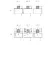
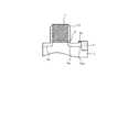
図1および図2は、フラッシュメモリの周辺回路部に形成したトランジスタの構成についてその断面と平面を示している。図2に示した平面図では、半導体基板としてのp型のシリコン基板1の一部を示しており、図示の左上に高電圧駆動PチャンネルトランジスタHV−P、右上に高電圧駆動NチャンネルトランジスタHV−N、左下に低電圧駆動PチャンネルトランジスタLV−Pを配置したものを代表的に示し、右下にはトランジスタを設けていない状態を示している。なお、周辺回路領域には実際には低電圧駆動Nチャンネルトランジスタも設けられるが、この実施形態においては特徴となる工程には関係していないので省略している。(First embodiment)
A first embodiment when the present invention is applied to a flash memory will be described below with reference to FIGS.
1 and 2 show a cross section and a plan view of the structure of the transistor formed in the peripheral circuit portion of the flash memory. In the plan view shown in FIG. 2, a part of a p-
図1(a)、(b)の各断面は、図2中A−A線およびB−B線で示す部分の縦断側面を示している。すなわち、図1(a)は、高電圧駆動PチャンネルトランジスタHV−Pおよび低電圧駆動PチャンネルトランジスタLV−Pのゲート電極を横切る方向の縦断面図であり、図1(b)は、高電圧駆動PチャンネルトランジスタHV−Pおよび高電圧駆動NチャンネルトランジスタHV−Nのゲート電極に沿う方向で不純物拡散領域部分の縦断面図である。 Each cross section of Drawing 1 (a) and (b) has shown the vertical section side of the portion shown by the AA line and BB line in FIG. That is, FIG. 1A is a longitudinal sectional view in a direction crossing the gate electrodes of the high voltage drive P-channel transistor HV-P and the low voltage drive P-channel transistor LV-P, and FIG. It is a longitudinal cross-sectional view of the impurity diffusion region in the direction along the gate electrodes of the driving P channel transistor HV-P and the high voltage driving N channel transistor HV-N.
図1(a)、(b)において、P型のシリコン基板1には、高電圧駆動PチャンネルトランジスタHV−Pおよび低電圧駆動PチャンネルトランジスタLV−Pのnウェル2、3が形成されている。また、高電圧駆動NチャンネルトランジスタHV−Nに対してはウェルを形成せず、p型のシリコン基板1を直接使用して形成する構成である。 1A and 1B, a P-
各ウェル2、3を形成した領域を素子形成領域とし、その周辺部分のシリコン基板1には、STI(Shallow Trench Isolation)4が形成されている。STI4は、後述するように、浅いトレンチを形成してこの内部にシリコン酸化膜などの絶縁膜を埋め込むことで形成している。 A region where the
STI4で囲まれたシリコン基板1の素子形成領域には、不純物をイオン注入により導入して拡散したソース・ドレインとなる不純物拡散領域5a、5bが形成されている。この場合、PチャンネルトランジスタHV−PおよびLV−Pにはp型の不純物拡散領域5aが形成され、NチャンネルトランジスタHV−Nにはn型の不純物拡散領域5bが形成されている。STI4の外周部には、シリコン基板1の表面が露出する領域としてガードリング1aが形成されている。この部分には、後述するように不純物が導入されるとともに、コンタクトをとることでガードリングとしての機能を達成している。
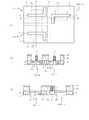
なお、低電圧駆動PチャンネルトランジスタLV−Pのシリコン基板1の表面は、後述するように、異なる膜厚のゲート絶縁膜6、8を同時にエッチングして剥離する関係から、少しエッチングにより掘り下がった状態(シリコンガウジング)となっており、高電圧駆動PチャンネルトランジスタHV−Pや高電圧駆動NチャンネルトランジスタHV−Nのシリコン基板1の表面高さに比べて低い位置となっている。 Note that the surface of the
上記のようにシリコンガウジングが発生するのは、ゲート絶縁膜6、8のエッチング条件として、シリコンに対する選択比を無限大に取ることができないからであり、低電圧駆動PチャンネルトランジスタLV−Pのゲート絶縁膜8がエッチングされてシリコン基板1の表面が先に露出し、高電圧駆動トランジスタHV−P、HV−Nのゲート絶縁膜6がエッチングされるまでの間、シリコン基板1の表面がエッチングされるからである。 The reason why the silicon gouging occurs as described above is that the etching condition of the
高電圧駆動トランジスタHV−P、HV−Nのシリコン基板1の表面には、不純物拡散領域5aあるいは5bのソース・ドレイン領域をはさむようにして膜厚が厚く形成されたゲート絶縁膜6およびゲート電極7が形成されている。ゲート絶縁膜6はシリコン酸化膜で形成されており、高電圧駆動用として膜厚がたとえば40nmである。 On the surface of the
また、ゲート電極7はゲート絶縁膜6の上に非晶質シリコン膜、ONO膜、多結晶シリコン膜、タングステンシリコン膜(WSi)などを積層して形成したもので、図示しないメモリセルトランジスタのゲート電極を形成する際に積層する膜構成となっている。この場合、ONO膜はメモリセルトランジスタのフローティングゲートを形成するためのものであり、周辺回路領域の各トランジスタのフローティングゲートは不要であるので、ONO膜に部分的に開口部を形成して上下の層間を電気的にショートさせるように形成している。 The
図1(b)では、高電圧駆動NチャンネルトランジスタHV−Nのゲート電極7がSTI4上に形成された状態に示されているが、これは、ゲートコンタクトを取るためのSTI4へのパターンが図示されたものである。
低電圧駆動PチャンネルトランジスタLV−Pのシリコン基板1の表面には、不純物拡散領域5aのソース・ドレイン領域をはさむようにして膜厚が薄く形成されたゲート絶縁膜8およびゲート電極7が形成されている。ゲート絶縁膜8はシリコン酸化膜で形成されており、低電圧駆動用として膜厚がたとえば8nmである。FIG. 1B shows a state in which the
On the surface of the
ゲート電極7を含んだシリコン基板1の表面にはバリア絶縁膜9が形成されている。バリア絶縁膜9は、たとえばシリコン窒化膜、シリコン酸窒化膜、酸化アルミニウム膜などからなり、エッチング処理のストッパとして機能させるものである。このバリア絶縁膜9の上には層間絶縁膜10が形成されている。層間絶縁膜10は、たとえば、シリコン酸化膜やシリコン窒化膜、あるいはBPSG、PSGなどのシリケートガラス、HSQやMSQ、SiLK(登録商標)などのlow−k材料からなるものである。 A
層間絶縁膜10には、各トランジスタHV−P、HV−N、LV−Pのソース・ドレインとコンタクトをとるために複数個のコンタクトホールが形成されており、その内周面には薄い膜厚のバリアメタル11が形成され、内部にはコンタクトプラグ12が埋め込み形成されている。この場合、バリアメタル11としては、たとえば、Ti、Ta、TaN、TiNなどが用いられる。また、コンタクトプラグ12は、タングステン、アルミニウムあるいは銅などの金属材料が用いられている。 A plurality of contact holes are formed in the
この上部には、上記した層間絶縁膜10と同様の材料からなる層間絶縁膜13が形成されており、その一部に第1のViaコンタクトホールが形成され、バリアメタル14を介して第1のViaコンタクトプラグ15が埋め込み形成されている。この第1のViaコンタクトプラグ15は、下地のコンタクトプラグ12と電気的に導通するように配置形成される。 An interlayer insulating
この層間絶縁膜13の上には、たとえばAlやAlCuなどの金属膜をパターニングして形成した第1の配線層16が形成されている。この第1の配線層16は、ビット線などの配線として形成されるものである。さらに、この上にはさらに前述と同様の材料からなる層間絶縁膜17が形成されている。この層間絶縁膜17には第2のViaコンタクトホールが形成され、バリアメタルを介してViaコンタクトプラグを兼ねた第2の配線層18がパターニング形成されている。第2の配線層18は、たとえば、タングステン、アルミニウムあるいは銅などからなる。この第2の配線層18は、層間絶縁膜19により埋め込まれた状態に形成されている。 On the
次に、上記構成についてその製造工程について図3〜図15も参照して説明する。
まず、図3(a)に示すように、p型シリコン基板1を洗浄後、基板汚染やリソグラフィの際のレジスト倒れ防止を目的に、犠牲酸化膜20を形成する。次いで、高電圧駆動PチャンネルトランジスタHV−Pおよび低電圧駆動PチャンネルトランジスタLV−Pの形成を目的とするリソグラフィ処理を行い、各トランジスタ領域のレジスト21を開口するパターニングをする。続いて、このレジスト21を利用して不純物としてP(リン)またAs(砒素)のイオンを1.0E+12〜14cm−2程度の条件で、シリコン基板1の表面に注入し、nウェル2、3を形成する。Next, the manufacturing process of the above configuration will be described with reference to FIGS.
First, as shown in FIG. 3A, after the p-
この後、注入した不純物イオンを活性化する必要があるため、不純物イオン注入後、通常800℃〜1200℃程度でアニールする工程が必要となるが、先ほど形成したNウェル2、3の他、pウェルを形成した後、まとめて活性化することもできる。不純物イオン注入後、マスクとして使用したレジストのパターン21は不要となるため、O2ドライアッシャや薬液処理により剥離し次工程へ進める。 After this, since it is necessary to activate the implanted impurity ions, a step of annealing at about 800 ° C. to 1200 ° C. is usually required after the impurity ions are implanted. In addition to the
次に、これまで使用していた犠牲酸化膜20をフッ酸等で剥離し、この後、ゲート絶縁膜6、8を形成する。この場合、これらのゲート絶縁膜6、8の膜厚は、低電圧駆動系トランジスタ領域についてはメモリセルアレイ領域のトランジスタと同等にすることが多いが、トランジスタ性能を高くするため、メモリセル領域のトランジスタとは異なる膜厚のゲート絶縁膜として形成することもある。 Next, the
高電圧駆動トランジスタHV−PおよびHV−Nのゲート絶縁膜6の形成後、低電圧駆動PチャンネルトランジスタLV−Pのゲート絶縁膜8を形成するために、一旦目的の領域に形成された上記ゲート絶縁膜6を除去する。このとき、高電圧駆動トランジスタHV−PおよびHV−Nのゲート絶縁膜6はそのまま残す必要があるので、図3(b)に示すように、リソグラフィ処理によりレジスト22をパターニングして、低電圧駆動PチャンネルトランジスタLV−Pの領域のみ開口し、フッ酸等でウェットエッチングして薄い膜厚のゲート絶縁膜6を除去する。この後、図3(c)に示すように、低電圧駆動トランジスタLV−Pの表面にゲート絶縁膜8を形成することで、膜厚の異なる2種類のゲート絶縁膜6、8がそれぞれに形成されることになる。 After the formation of the
次に、図4(d)に示すように、メモリセル領域のセルトランジスタ(図示せず)に形成するフローティングゲート電極の構成として、ノンドープの非晶質シリコン膜23をLP−CVD(Low Pressure-Chemical Vapor Deposition)法により膜厚40nm程度で堆積させる。
続いて、低電圧駆動PチャンネルトランジスタLV−PのNウェル3にトランジスタの閾値を所定のレベルとなるように設定するために、不純物を導入する。このため、リソグラフィ処理によりレジスト24をパターニングして低電圧駆動PチャンネルトランジスタLV−Pのnウェル3の表面部分を開口させる。Next, as shown in FIG. 4D, as a structure of a floating gate electrode formed in a cell transistor (not shown) in the memory cell region, a non-doped
Subsequently, impurities are introduced into the N well 3 of the low voltage drive P-channel transistor LV-P in order to set the threshold value of the transistor to a predetermined level. Therefore, the resist 24 is patterned by lithography to open the surface portion of the n-well 3 of the low voltage drive P-channel transistor LV-P.
このレジスト24をマスクとして、目的の箇所にB(ボロン:ホウ素)等の不純物イオンを1.0E+12〜14cm−2程度の条件で、堆積したフローティングゲート電極となる非晶質シリコン膜23越しにシリコン基板1に注入する(図4(d)参照)。フローティングゲート電極越しに不純物イオンを注入する場合、ゲート絶縁膜8の形成前に不純物イオンを注入する場合と比べて、注入した不純物イオンのシリコン基板1内での不純物濃度を高くすることができるというメリットがある。 Using this resist 24 as a mask, impurity ions such as B (boron: boron) are deposited at a target location under the condition of about 1.0E + 12 to 14 cm −2 through the
また、ゲート絶縁膜8の形成前に不純物イオンを注入する方法では、ゲート絶縁膜8の形成時の熱工程により、不純物イオンがシリコン基板1中を拡散するため、実効的な濃度が低下し所望の閾値電圧を得るのが困難となる。不純物イオン注入の後、マスクとして使用したレジスト24は不要となるため、O2ドライアッシャあるいは薬液処理により剥離する。 Further, in the method of implanting impurity ions before the formation of the
次に、p型シリコン基板1上に形成する高電圧駆動NチャンネルトランジスタHV−Nの閾値を設定するためのリソグラフィ処理を実施し、レジスト26をパターニングしてイオン注入対象領域である高電圧駆動NチャンネルトランジスタHV−Nの部分を開口させる。この処理では、図4(e)に示すように、目的の箇所にB(ボロン)等の不純物イオンを1.0E+11〜14cm−2程度の注入条件で、堆積したフローティングゲート電極23越しにシリコン基板1に注入する。フローティングゲート電極23越しに不純物イオンを注入する場合のメリットは、先に説明した通りである。不純物イオン注入後、マスクとして使用したレジスト26は不要となるため、O2ドライアッシャや薬液処理により剥離し次工程へ進める。 Next, a lithography process for setting the threshold value of the high-voltage drive N-channel transistor HV-N formed on the p-
次に、シリコン基板1の非晶質シリコン膜23を積層した構成の上に、シリコン窒化膜、シリコン酸化膜などを積層形成し、この後、リソグラフィ処理によりレジストをパターニングしてSTI4の形成領域の部分を開口する。レジスト26をマスクとして、RIE法によりシリコン酸化膜をエッチングし、さらに、シリコン酸化膜をマスクとしてシリコン窒化膜、非晶質シリコン膜23、ゲート絶縁膜6、8およびシリコン基板1を順次エッチングし、シリコン基板1に深さが0.1μmから0.4μm程度のトレンチを形成し、その内部にシリコン酸化膜あるいはシリコン窒化膜からなる絶縁膜を埋め込み形成し、STI4を形成する。この場合のSTI4による素子分離の深さは、STI4を介して隣接するnウェル2、3などが互いに分離される程度としている。 Next, a silicon nitride film, a silicon oxide film, and the like are laminated and formed on the laminated structure of the
次に、ウェル分離をしていない、p型シリコン基板1上に直接形成されたNチャンネルトランジスタ間のパンチスルー電圧駆動を向上すべく、層間絶縁膜越しに、高濃度フィールドスルーストッパとしてリン等の不純物イオンを注入する。 Next, in order to improve the punch-through voltage drive between the N-channel transistors directly formed on the p-
続いてリン等の不純物を高濃度でドープした多結晶シリコン膜若しくはタングステンシリサイド膜等の導電体膜を500nmから1000nm程度堆積させた後、リソグラフィ処理によりレジストをデータ転送線となる形状にパターニングを行い、異方性エッチングを行ってゲート電極7を形成し、図5(a)に示すような状態とする。この際、エッチング条件はレジストおよびマスク材、ゲート絶縁膜6、8に対して選択比を持つように設定している。 Subsequently, after depositing a conductor film such as a polycrystalline silicon film or tungsten silicide film doped with impurities such as phosphorus at a high concentration of about 500 nm to 1000 nm, the resist is patterned into a shape to be a data transfer line by lithography processing. Then, anisotropic etching is performed to form the
次に、図5(b)に示すように、高電圧駆動トランジスタHV−P、HV−Nおよび低電圧駆動PチャンネルトランジスタLV−Pの各ゲート絶縁膜6、8を除去する。ここでは、高電圧駆動トランジスタHV−P、HV−Nのゲート絶縁膜6を除去時に、同時に低電圧駆動PチャンネルトランジスタLV−Pのゲート絶縁膜8も除去する。この際、リソグラフィ処理でレジストをパターニングする場合には、目的箇所以外のセル部、セルコンタクト部および低電圧駆動Nチャンネルトランジスタのゲート絶縁膜部分はレジストを残した状態として開口しないようにしている。 Next, as shown in FIG. 5B, the
なお、高電圧駆動トランジスタHV−P、HV−Nのゲート絶縁膜6は、先にも述べたように低電圧駆動PチャンネルトランジスタLV−Pのゲート絶縁膜8に対して5倍程度も厚く形成しているため、高電圧駆動トランジスタHV−P、HV−Nのゲート絶縁膜6をRIE等で完全に除去する場合に、低電圧駆動PチャンネルトランジスタLV−Pのゲート絶縁膜8はかなりオーバーエッチングされてしまう。 The
そのため、エッチング条件はシリコン基板1との高い選択比を有することが必要であるが、選択比については高くても30程度であるため、低電圧駆動トランジスタのシリコン基板1の表面は図5(b)に示しているように、多少掘られてしまう現象が発生する(本現象を以下シリコンガウジングと称する)。したがって、本実施形態の製造方法を採用する場合には、低電圧駆動PチャンネルトランジスタLV−Pがシリコンガウジングを有することが大きな特徴となる。 Therefore, the etching condition needs to have a high selection ratio with respect to the
低電圧駆動PチャンネルトランジスタLV−Pは、ゲート絶縁膜8を除去することで、除去しない場合と比べて、不純物注入を同条件とした場合に、不純物イオンの基板濃度ピークが深く形成されるようになる。それを考慮すれば、ゲート絶縁膜8の除去時に不純物注入の電圧加速を低下させると、これによって不純物イオン注入時の投影飛程Rpが低下し、同時に揺らぎ(標準偏差)ΔRpも低減できるようになる。この結果、S/D(ソース/ドレイン)間の実効チャンネル長を抑えることが可能になり、結果トランジスタの閾値変動を抑制することが可能となる。 In the low-voltage drive P-channel transistor LV-P, by removing the
また、低電圧駆動PチャンネルトランジスタLV−Pの拡散層に、高電圧駆動トランジスタの不純物領域と同程度の不純物注入を行う場合、ゲート絶縁膜の膜厚依存性がなくなるため、高電圧駆動トランジスタと低電圧駆動トランジスタの拡散層不純物イオン注入条件を共通化できるメリットもある。さらにゲート絶縁膜8の除去時にリソグラフィ処理によりレジストのパターニングを行うが、高電圧駆動トランジスタHV−P、HV−Nの領域と目的の低電圧PチャンネルトランジスタLV−Pを同時に開口した場合、ゲート絶縁膜6、8の除去後に、形成したレジストパターンをそのまま使用し、拡散層不純物注入を行うこともでき、結果として工程簡略化が可能となる。 In addition, when the impurity implantation of the same degree as the impurity region of the high voltage driving transistor is performed in the diffusion layer of the low voltage driving P channel transistor LV-P, the film thickness dependency of the gate insulating film is eliminated. There is also a merit that the diffusion layer impurity ion implantation conditions of the low voltage driving transistor can be made common. Further, resist patterning is performed by lithography processing when the
図6は上記のようにして形成された状態の平面図および断面図を示すもので、図6(a)は図2に示した平面図に対応し、図6(b)、(c)は、図1に示した断面図に対応している。この状態では、シリコン基板1の上面に形成した層間絶縁膜10にレジストパターン27により開口部が形成され、ゲート絶縁膜6、8を剥離して不純物拡散層5a、5bを形成したところである。低電圧駆動PチャンネルトランジスタLV−Pの不純物拡散層5aの表面はシリコン基板1が少し掘り下がった状態つまりシリコンガウジングが発生していることがわかる。 FIG. 6 shows a plan view and a cross-sectional view of the state formed as described above. FIG. 6 (a) corresponds to the plan view shown in FIG. 2, and FIGS. 6 (b) and 6 (c) 1 corresponds to the cross-sectional view shown in FIG. In this state, an opening is formed by the resist
次に、図7に示すように、シリコン基板1およびゲート電極7を覆うように、シリコン窒化膜やシリコン酸窒化膜、または、酸化アルミニウム膜からなるバリア絶縁膜9を10nmから1000nmの範囲で堆積する。このバリア絶縁膜9は、次の目的で形成されたものである。
すなわち、層間絶縁膜10へのコンタクトホールの形成時にエッチング制御性が不足し、エッチングが過剰に行われると、コンタクトホールがSTI4(素子分離領域)に落ち込みシリコン基板1とコンタクトとの電圧駆動が確保できない問題が生ずる。一方、コンタクト形成時にエッチングが不足すると、n型領域とデータ転送線コンタクトとの間のコンタクト抵抗が上昇する問題が生じる。Next, as shown in FIG. 7, a
That is, when the contact hole is formed in the
そこで、このコンタクトを形成時に、層間絶縁膜10に対してバリア絶縁膜9を設けることでエッチングスピードが遅く選択比が取れる条件でエッチングし、さらに、バリア絶縁膜9をその後でエッチングすることにより、コンタクトエッチングする時の層間絶縁膜10の膜厚変動の影響を低減することができる。 Therefore, when this contact is formed, the
また、このバリア絶縁膜9を堆積する前に、シリコン基板1の表面に酸化または堆積法により1nmから50nmの範囲のシリコン酸化膜を作成しても良い。さらに、その上にシリコン酸化膜、シリコン窒化膜やBPSG,PSGなどのシリケードガラス、HSQ(Hydrogen Silsequioxanes)やMSQ(Methyl Silsequioxanes)、SiLKなどの層間膜からなる層間絶縁膜10を10〜1000nm程度堆積する。
バリア絶縁膜9の材料は層間絶縁膜10に対するエッチング選択比を持つことが必要である。バリア絶縁膜1の厚さは10〜1000nm程度で、層間絶縁膜10の厚さとエッチング選択比によって十分な加工マージンを有する厚さを必要とする。Further, before depositing the
The material of the
次に、リソグラフィ処理によって、レジスト28のパターニングを行い、図8に示すように、データ選択線(ゲート電極7)上コンタクトおよび基板ソース・ドレインコンタクトの開口10aを形成する。このレジスト28をマスクとして、層間絶縁膜10を異方性エッチングによってパターニングする。この際、エッチング条件はレジスト28およびバリア絶縁膜9に対して選択比を持つ条件であることが必要である。 Next, the resist 28 is patterned by a lithography process to form
ついで、レジスト28の除去後に、図9に示すように、コンタクトホール10aの底面部に露出しているバリア絶縁膜9を異方性エッチングする。この際、シリコン基板1、層間絶縁膜10に対して選択比を有する条件で実施することが、後工程において、バリア絶縁膜9を剥離するウェット工程を必要とせず、また層間絶縁膜10に対する後退がなく、順テーパ形状を維持し、コンタクト径を小さく保てるため望ましい。 Next, after removing the resist 28, as shown in FIG. 9, the
この後、例えば、リンや砒素不純物を、例えば1×1013cm-2以上1×1016cm-2以下のドーズでイオン注入して、コンタクトホール10a部分のn型領域の抵抗率を低下させてもよい。一方、B(ホウ素)、BF2(2フッ化ホウ素)不純物を例えば1×1013cm-2以上1×1016cm-2以下のドーズ量でイオン注入して、コンタクトホール10a部分のp型領域の抵抗率を同様に低下させてもよい。Thereafter, for example, phosphorus or arsenic impurities are ion-implanted with a dose of 1 × 1013 cm−2 or more and 1 × 1016 cm−2 or less, for example, to reduce the resistivity of the n-type region in the
続いて、ソース・ドレインコンタクトおよび、データ選択線のコンタクトホール10aに接続される引き出し配線のリソグラフィ処理で、レジスト29のパターニングを行い、図10に示すように、層間絶縁膜10を異方性エッチングによってパターニングし配線用開口部10bを形成する。 Subsequently, the resist 29 is patterned by lithography processing of the source / drain contact and the lead wiring connected to the
その後、レジスト29を除去し、Ti、Ta、TaN、TiN等のバリアメタル11を,1nmから100nmの範囲で、例えばスパッタやCVD法によってコンタクトホール10a及び配線用開口部10b内に堆積した後に、タングステン、アルミ、銅等の金属材料を10nmから1000nmの厚さで堆積し、コンタクトホール10a及び配線用開口部10b内に埋め込む。その後、CMP(Chemical Mechanical Polishing)等で平坦化し、図11に示すような構成を得る。この場合、バリアメタル11としては、CVD法の方が、よりアスペクトが高いコンタクトホール10aに均一に堆積できるため望ましい。 Thereafter, the resist 29 is removed, and a
その後、シリコン酸化膜やBPSG,PSGなどのシリケードガラスや、HSQ、MSQやSiLKなどの層間膜からなる層間絶縁膜13を10〜1000nm程度堆積する。次に、リソグラフィ処理によってレジスト30について、第1のViaコンタクトホール13aのパターニングを行う。続いて、図12に示すように、レジスト30をマスクとして、層間絶縁膜13を異方性エッチングによって第1のViaコンタクトホール13aを形成する。エッチング条件はレジストおよび下層コンタクトに埋め込まれた金属またはバリアメタルに対して選択比を持つ条件であることが必要である。 Thereafter, an
ついで、レジスト30の除去後Ti、Ta、TaN、TiN等のバリアメタルを1nmから100nmの範囲で、例えばスパッタやCVD法によって第1のViaコンタクトホール13a内に堆積した後に、タングステン、アルミニウム、銅等の金属材料を10nmから1000nmの厚さで堆積し、第1のViaコンタクトホール13aを埋め込むようにする。その後、CMP等でエッチバックし平坦化し、図13に示すような形状のものを確保する。
Next, after removing the resist 30, a barrier metal such as Ti, Ta, TaN, TiN or the like is deposited in the first via
その後は、図14に示すように、例えば、AlあるいはAlCuを10〜1000nm程度堆積する。さらに、異方性エッチングにより、前記AlまたはAlCuをA−A方向に短冊状に加工し、データ転送線となる配線層16を形成する。この後、シリコン酸化膜、シリコン窒化膜やBPSG,PSGなどのシリケードガラスや、HSQやMSQ、SiLKなどの層間膜からなる層間絶縁膜17を10〜1000nm程度堆積する。 Thereafter, as shown in FIG. 14, for example, Al or AlCu is deposited to a thickness of about 10 to 1000 nm. Further, the Al or AlCu is processed into a strip shape in the AA direction by anisotropic etching to form a
次に、リソグラフィ処理によってレジスト31を塗布して第2のViaコンタクトホール17aのパターニングを行い、図15に示すように、層間絶縁膜17を異方性エッチングによってパターニングする。エッチング条件はレジスト31および下層コンタクトに埋め込まれた金属またはバリアメタルに対して選択比を持つ条件であることが必要である。 Next, a resist 31 is applied by lithography to pattern the second via
ついで、レジスト31の除去後Ti、Ta、TaN、TiN等のバリアメタルを1nmから100nmの範囲で、例えばスパッタやCVD法によって第2のViaコンタクトホール17a内および層間絶縁膜上に堆積した後に、タングステン、アルミニウム、銅等の金属材料を10nmから1000nmの厚さで堆積し、第2のViaコンタクトホール17a内を埋め込むと同時にソース線18の配線材料としても同時に堆積する。 Next, after removing the resist 31, after depositing a barrier metal such as Ti, Ta, TaN, TiN in the range of 1 nm to 100 nm, for example, in the second via
もちろん第1のViaコンタクトホール13aおよびデータ転送線の製造法で示したように、コンタクトホール17aの内部をTi、Ta、TaN、TiN等のバリアメタルで1nmから100nmの範囲で例えばスパッタやCVD法によって堆積した後に、タングステン、アルミニウム、銅等の金属材料を10nmから1000nmの厚さで堆積し、第2のViaコンタクトホールを埋め込みCMP等で平坦化した後に配線材として、Al、AlCuを10〜1000nm程度堆積する方法もあるが、本実施例では、Viaコンタクト2とソース線2の導電性材料を同時に堆積することでプロセス工程の簡略化が可能であることを示している。 Of course, as shown in the manufacturing method of the first via
最後にリソグラフィによって、堆積したAl、AlCu等10〜1000nm程度を、異方性エッチングにより加工することにより、本実施例の形状が得られる。
このような本実施形態によれば、ゲート電極7の形成後に高電圧駆動トランジスタHV−P、HV−Nのゲート絶縁膜6をRIE等で除去する際、低電圧駆動PチャンネルトランジスタLV−Pのゲート絶縁膜8も同時に除去することにより、その後に行われるN−拡散層形成向けのチャンネル不純物イオン注入を、加工時に用いたレジストをそのままマスクとして同時に形成することができ、これによってリソグラフィ処理を簡略化でき、リソグラフィ処理の回数を削減して工程短縮およびコスト低減を図ることができるようになる。Finally, the shape of this embodiment can be obtained by processing about 10 to 1000 nm of deposited Al, AlCu, etc. by anisotropic etching by lithography.
According to the present embodiment, when the
上述の場合に、低電圧駆動PチャンネルトランジスタLV−Pのゲート絶縁膜8の膜厚が薄いことから、同時にRIEを実施したときにシリコンガウジングが発生するが、このことによるショートチャンネル効果の影響については、例えば不純物イオンをHaloインプランテーションすることで解消することができるようになる。 In the above case, since the
また、このように、高電圧駆動トランジスタHV−P、HV−Nの拡散層5aと、低電圧駆動PチャンネルトランジスタLV−Pの拡散層5bを形成するのに、不純物イオン注入を同時に実施するので、これによって、両者の不純物プロファイルを揃えることができるとともに、ひとつの不純物プロファイルを設定することで特性を調整するための制御性を高めることができるようになる。 In addition, since the
また、メモリセル領域のトランジスタおよび低電圧駆動Nチャンネルトランジスタについては、高電圧駆動トランジスタ用N−拡散層で使用したチャンネル不純物イオン注入を行わないので、個別に拡散層エンジニアリングが可能になり、ショートチャンネル効果を抑制することも可能となる。 In addition, for the transistor in the memory cell region and the low-voltage drive N-channel transistor, the channel impurity ion implantation used in the N-diffusion layer for the high-voltage drive transistor is not performed. It is also possible to suppress the effect.
(第2の実施形態)
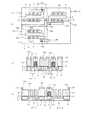
図16および図17は本発明の第2の実施形態を示すもので、第1の実施形態と異なるところは、ゲート電極形成後に、残ったゲート絶縁膜を除去する工程で、第1の実施形態では、高電圧駆動トランジスタHV−P、HV−Nのゲート絶縁膜6を除去時に、同時に低電圧駆動PチャンネルトランジスタLV−Pのゲート絶縁膜8も除去したが、この実施形態では、メモリセルトランジスタのセルコンタクト部についても、同時にゲート絶縁膜を除去するところである。(Second Embodiment)
FIGS. 16 and 17 show a second embodiment of the present invention. The difference from the first embodiment is that the remaining gate insulating film is removed after the formation of the gate electrode in the first embodiment. Then, when removing the
つまり、高電圧駆動トランジスタHV−P、HV−N、低電圧駆動PチャンネルトランジスタLV−Pに加えて、メモリセル領域40のセレクトゲートに形成するセルコンタクト部41についてもゲート絶縁膜42が同時に除去されるようにレジスト43を開口形成したものである(図17で斜線領域がレジスト43の形成領域)。この場合、メモリセル部40のセルトランジスタの形成領域および図示しない周辺回路領域の低電圧駆動Nチャンネルトランジスタ部のゲート絶縁膜はリソグラフィ処理によりレジスト43が選択的に残される。 That is, in addition to the high voltage drive transistors HV-P and HV-N and the low voltage drive P channel transistor LV-P, the
高電圧駆動トランジスタHV−P、HV−Nのゲート絶縁膜6は先にも述べたように、低電圧駆動トランジスタのゲート絶縁膜8の5倍程度厚いため、高電圧駆動トランジスタ領域のゲート絶縁膜6をRIE等で完全に除去する場合、セルコンタクト部および低電圧Pチャンネルトランジスタ部はかなりオーバーエッチングされてしまう。そのため、エッチング条件はシリコン基板1との高い選択比を有する事が必要であるが、選択比は高くても30程度であるため、セルコンタクト部41および低電圧駆動トランジスタ部のシリコン面は多少掘られてしまう現象が発生する。 As described above, the
よって本実施例では、セルコンタクト部および低電圧駆動Pチャンネルトランジスタがシリコンガウジングを有する構造となるが、このことはセルコンタクト部に対して大きな影響を与えることはなく、むしろ、これによって接触抵抗の低減を図ることができるという利点がある。 Therefore, in this embodiment, the cell contact portion and the low voltage drive P-channel transistor have a structure having silicon gouging. However, this does not have a great influence on the cell contact portion, but rather, the contact resistance is reduced. There is an advantage that reduction can be achieved.
このような第2の実施形態によれば、第1の実施形態のものと異なり、セルコンタクト部41のゲート絶縁膜42も除去することで、コンタクト抵抗を低減できるという効果を得ることができる。 According to the second embodiment, unlike the first embodiment, it is possible to obtain an effect that the contact resistance can be reduced by removing the
(第3の実施形態)
図18ないし図24は本発明の第3の実施形態を示すもので、第1の実施形態と異なるところは、ゲート電極7の形成後に残ったゲート絶縁膜を除去する工程である。第1の実施形態では、高電圧駆動トランジスタHV−P、HV−Nのゲート絶縁膜6および低電圧駆動PチャンネルトランジスタLV−Pのゲート絶縁膜8を除去する場合に、シリコン基板1の素子形成領域が露出している領域、つまりSTI4の形成領域との境界部分までを対象としていたが、この実施形態では、高電圧駆動トランジスタHV−P、HV−Nについて、STI4の形成領域よりも少し内側の領域を除去するようにしたところが異なる特徴である。(Third embodiment)
18 to 24 show a third embodiment of the present invention. The difference from the first embodiment is a step of removing the gate insulating film remaining after the
このことは、高電圧駆動トランジスタHV−P、HV−Nの形成領域について、ゲート絶縁膜6の除去の際に、STI4の形成領域を含んでレジストを開口してエッチング処理を行うことの弊害を防止することに効果がある。すなわち、厚いゲート絶縁膜6のエッチングに際してSTI4が露出するマスクパターンを用いると、ゲート絶縁膜6のエッチングを確実に行うためにオーバーエッチングを実施したときに、STI4も同時に掘り下げられてしまうことになる。 This has the adverse effect of performing etching by opening the resist including the
STI4の上面高さは、シリコン基板1の表面とほぼ同じ高さまで落とし込まれているので、さらにSTI4がエッチングで掘り下げられると、後の不純物導入工程で隣接するシリコン基板1への不純物導入が掘り下げられている部分だけ部分的に深く不純物が注入されてしまい、このことがSTI4を挟んで隣接するトランジスタとの間で絶縁距離を短くしてしまうことになり、電気的特性の低下を招くことになっていたのである。 Since the upper surface height of the
そこで、この実施形態では、ゲート電極7の加工後、不純物イオン注入等のために、厚いゲート酸化膜6を持つ高電圧用トランジスタHV−P、HV−Nの形成領域において、シリコン基板1上に存在するゲート酸化膜6を除去する際、被エッチング領域をトランジスタ素子領域内に限定し、STI4に充填されているシリコン酸化膜の基板表面からの落ち込みを防ぐことで、STI4近傍において不純物拡散層が深く形成されてしまうことを防止し、トランジスタ素子の電圧駆動劣化を抑制することが可能としたものである。 Therefore, in this embodiment, after processing the
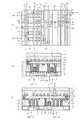
以下、図18に示すような高電圧駆動PチャンネルトランジスタHV−Pの一部の構成を例としてこの実施形態の特徴について説明をする。図18は、第1の実施形態における図11の構成に対応するもので、層間絶縁膜10、10A(層間絶縁膜10は、実際には複数の層を積層したものであるから、ここでは上部のものを層間絶縁膜10Aとして示している)にコンタクトプラグ12を形成した状態を示している。 Hereinafter, the characteristics of this embodiment will be described by taking as an example a configuration of a part of the high-voltage drive P-channel transistor HV-P as shown in FIG. FIG. 18 corresponds to the configuration of FIG. 11 in the first embodiment. The
図中、シリコン基板1のSTI4との境界部分の表面には、ゲート絶縁膜6の一部として絶縁膜6aが残った状態で示されている。これは、加工前の状態ではゲート絶縁膜6と同じ膜厚になっていたものが、後述するように加工工程を経ることでエッチングが進行して膜厚が薄くなったものである。 In the drawing, the insulating
また、この実施形態では、不純物拡散領域5aの部分のシリコン基板1の表面に僅かながら2段にシリコンガウジングが発生した状態となっている。具体的には、シリコン基板1の表面の高さが、ゲート絶縁膜6が形成された部分に比べて、スペーサ51の形成部分では少し下がっており、コンタクト形成領域ではさらに下がった位置となっている。 In this embodiment, the silicon gouging is slightly generated in two steps on the surface of the
このようにシリコンガウジングが発生するのは、シリコン基板1の上面に形成されている膜をRIE法などでエッチングする際に、選択比が無限大とならないことに起因したもので、工程ばらつきを考慮して膜が除去された後シリコン基板1の表面が露出した状態でエッチング処理が継続されるからである。なお、図ではシリコンガウジングが発生している状態を誇張して示している。 Such silicon gouging is caused by the fact that the selection ratio does not become infinite when the film formed on the upper surface of the
図19は、高電圧駆動PチャンネルトランジスタHV−Pの平面図を示しており、A−A線が図18に示す切断線であり、図中、破線Sで示す線はその内側のゲート絶縁膜6を除去するレジストパターンを示すもので、ゲート絶縁膜6のパターン残りとして絶縁膜6aが残った状態を示している。 FIG. 19 shows a plan view of the high-voltage drive P-channel transistor HV-P, wherein the AA line is a cut line shown in FIG. 18, and the line indicated by a broken line S in FIG. 6 shows a resist pattern for removing 6, and shows a state in which the insulating
次に、上記構成の製造工程について説明する。
図20は高電圧駆動PチャンネルトランジスタHV−Pのゲート電極7を加工形成した状態を示している。これは、第1の実施形態における図5(a)の状態に対応している。
この状態から、図21に示すように、高電圧駆動用PチャンネルトランジスタHV−Pのシリコン基板1上(ソース/ドレイン領域)に存在する35nm程度の厚いゲート絶縁膜6をエッチングし除去する。この時、本実施例では図19中破線Sで示すようにエッチングを行なう領域を高電圧駆動PチャンネルトランジスタHV−P内に限定する。具体的には、STI4の内側になるように領域を限定することで、図示のようにSTI4がシリコン基板1から落ち込むのを防ぐことが出来るが、STI4の脇にゲート絶縁膜6がエッチングされずに6aとして残る。Next, the manufacturing process of the said structure is demonstrated.
FIG. 20 shows a state in which the
From this state, as shown in FIG. 21, the thick
次に、後酸化を行なった後、拡散層形成のためイオン注入を行なう。ここでは、低電圧駆動NチャンネルトランジスタはLDD(Lightly Doped Drain)構造とし例えばAs(砒素)を20keVで3.0E13[atoms/cm2]の条件で不純物注入を行いN−層を形成する。この時、同時にメモリセル領域のセルアレイ部のN−拡散層を形成する。また、高電圧駆動PチャンネルトランジスタHV−Pについては、図22に示すように、HaloインプラとしてP(リン)を30keVで4.5E12[atoms/cm2]の条件でイオン注入を行なう。この時、STI4の脇には厚いゲート絶縁膜6aが残っているため、STI4の隣接部分では不純物の平均射影飛程が短くなることに注意が必要である。 Next, after post-oxidation, ion implantation is performed to form a diffusion layer. Here, the low-voltage drive N-channel transistor has an LDD (Lightly Doped Drain) structure and, for example, As (arsenic) is implanted at 20 keV under the condition of 3.0E13 [atoms / cm 2] to form an N− layer. At the same time, an N− diffusion layer of the cell array portion in the memory cell region is formed. As for the high-voltage drive P-channel transistor HV-P, as shown in FIG. 22, ion implantation is performed under the condition of 4.5E12 [atoms / cm 2] at 30 keV as P (phosphorus) as a Halo implant. At this time, since the thick
次に、図23に示すように、WL間の埋め込み及び、周辺トランジスタ部の側壁スペーサ51の形成のため、従来と同様にTEOS膜を80nm成膜しエッチバックを行なう。この際のオーバーエッチングによりSTI4の脇に存在するゲート絶縁膜6aは膜厚が薄くなる。具体的には、TEOS膜の膜厚が80nmであるのに対し30%程度のオーバーエッチングを行なうため、図示のように、STI4の脇に残るゲート絶縁膜6は膜厚が10nm以下程度となる。この時、STI4についても同様にエッチングされ、その高さがシリコン基板1の表面近傍の位置となるように調整される。 Next, as shown in FIG. 23, a TEOS film is formed to a thickness of 80 nm and etched back in the same manner as in the prior art in order to fill the WL and to form the
次に、トランジスタのソース/ドレイン領域に拡散層形成のため、NチャンネルトランジスタHV−NにはAs(砒素)を、PチャンネルトランジスタHV−PにはB(ホウ素)を3.0×E15[atoms/cm2]程度の条件でイオン注入行い、図示の場合ではP+拡散層5aを形成する。この時、STI4の脇には若干ゲート絶縁膜6aが残っており、高電圧駆動トランジスタHV−P、HV−NではSTI4の脇における拡散層5aaのようには若干浅く形成される。 Next, in order to form a diffusion layer in the source / drain region of the transistor, As (arsenic) is used for the N channel transistor HV-N, and B (boron) is used for the P channel transistor HV-P by 3.0 × E15 [atoms. / Cm <2>], ion implantation is performed to form a P +
この後、従来と同様にして、シリコン窒化膜をバリア絶縁膜9として膜厚20nmで堆積した後、ゲート電極間をBPSG膜で埋め込み、CMP法により平坦化を行ない層間絶縁膜10を形成する。次に、層間絶縁膜10AとしてプラズマTEOS膜を250nm成膜した後、ビット線コンタクト及び周辺回路部にコンタクトホールを開口する。続いて、配線層となる溝を形成した後、ビット線コンタクトとコンタクトホール及び配線溝を、バリアメタル11としてTi/TiNを積層でスパッタ法により成膜した後、CVD法にてコンタクトプラグ12を充填する。次に、CMP法により平坦化を行い、図18の構成を得る。以後、バックエンド工程へと進めて行く。 Thereafter, in the same manner as in the prior art, a silicon nitride film is deposited as a
上記方法を用いることにより、周辺回路、特に高電圧駆動トランジスタHV−P、HV−NにおいてSTI4がシリコン基板1より落ち込むことを防ぎ、隣接トランジスタ間のパンチスルー電圧駆動劣化を改善することで、STI4の形成幅を縮小し、チップ面積を低減することが可能となる半導体装置を提供することが出来る。 By using the above method, it is possible to prevent the
なお、本実施形態では、STI4の脇にゲート絶縁膜6aが残り、この部分がゲート電極近傍にイオン注入される不純物プロファイルとは異なるため、イオン注入条件を最適化する際は、ゲートエッジ部でのショートチャンネル特性悪化によるオフリーク不良等が生じないように条件を決定する必要がある。 In this embodiment, the
図面中、1はシリコン基板(半導体基板)、2、3はNウェル、4はSTI(素子分離領域)、6、8はゲート絶縁膜、9はバリア絶縁膜、10、13、17、19は層間絶縁膜、11、14はバリアメタル、12は第1のViaコンタクトプラグ、15は第2のViaコンタクトプラグ、16は第1の配線層、18は第2の配線層である。 In the drawings, 1 is a silicon substrate (semiconductor substrate), 2 and 3 are N wells, 4 is an STI (element isolation region), 6 and 8 are gate insulating films, 9 is a barrier insulating film, 10, 13, 17, and 19 are Interlayer insulating films, 11 and 14 are barrier metals, 12 is a first via contact plug, 15 is a second via contact plug, 16 is a first wiring layer, and 18 is a second wiring layer.
Claims (5)
Translated fromJapaneseゲート電極を構成する膜を積層形成する工程と、
積層形成した膜をエッチングにより分離してゲート電極を形成する工程と、
これらのゲート電極を構成要素として含むトランジスタの所定の不純物拡散領域形成部分についてその表面の前記膜厚の異なるゲート絶縁膜を開口するためのマスクパターンを形成する工程と、
形成された前記マスクパターンを用いて前記膜厚の異なるゲート絶縁膜を剥離すると共に、前記マスクパターンを用いて前記薄い膜厚のゲート絶縁膜を構成要素として含むPチャンネルトランジスタと、前記厚い膜厚のゲート絶縁膜を構成要素として含むNおよびPチャンネルトランジスタに対し、N−拡散層を形成するためにそのゲート絶縁膜を剥離した開口部に不純物を導入する工程と、
を備え、
前記マスクパターンを形成する工程は、リソグラフィ工程を含み、
前記リソグラフィ工程は、前記薄い膜厚のゲート絶縁膜を構成要素として含むNチャンネルトランジスタの前記ゲート絶縁膜部分にレジストを残すことを特徴とする半導体装置の製造方法。Forming a gate insulating film having a different film thickness including at least a thick film thickness and a thin film thickness on a semiconductor substrate;
A step of laminating a film constituting the gate electrode;
Separating the stacked films by etching to form a gate electrode;
Forming a mask pattern for opening a gate insulating film having a different thickness on the surface of a predetermined impurity diffusion region forming portion of a transistor including these gate electrodes as components; and
Using the formed mask pattern, the gate insulating film having a different thickness is peeled off,and using the mask pattern, the P channel transistor including the thin gate insulating film as a constituent element, and the thick film thickness Introducing an impurity into an opening fromwhich the gate insulating film has been peeled toform an N- diffusion layer for N and P channel transistors including the gate insulating film as a component ;
With
The step of forming the mask pattern includes a lithography step,
In the lithography process, a resist is left in the gate insulating film portion of the N-channel transistor including the thin gate insulating film as a constituent element.
前記半導体基板の前記トランジスタ形成領域に溝を形成して絶縁膜を埋め込んだ構成の素子分離領域を有する場合に、
前記マスクパターンを形成する工程では、前記半導体基板の表面の前記素子分離領域との境界部分よりも内側領域を開口するようにパターニングすることを特徴とする半導体装置の製造方法。In the manufacturing method of the semiconductor device according to claim 1,
When having an element isolation region having a structure in which a trench is formed in the transistor formation region of the semiconductor substrate and an insulating film is embedded,
In the step of forming the mask pattern, patterning is performed so that an inner region is opened from a boundary portion between the surface of the semiconductor substrate and the element isolation region.
前記半導体装置は、メモリセル領域および周辺回路領域を含んで構成され、
前記トランジスタは、前記周辺回路領域のトランジスタを対象として形成されることを特徴とする半導体装置の製造方法。In the manufacturing method of the semiconductor device according to claim 1 or 2,
The semiconductor device includes a memory cell region and a peripheral circuit region,
The method of manufacturing a semiconductor device, wherein the transistor is formed for a transistor in the peripheral circuit region.
前記トランジスタは、前記ゲート絶縁膜が厚く形成されている高電圧駆動トランジスタおよび前記ゲート絶縁膜が薄く形成されている低電圧駆動トランジスタを共に含んだ構成のものであることを特徴とする半導体装置の製造方法。In the manufacturing method of the semiconductor device according to claim 3,
The transistor includes a high voltage driving transistor in which the gate insulating film is formed thick and a low voltage driving transistor in which the gate insulating film is formed thin. Production method.
前記ゲート絶縁膜を剥離する工程では、前記高電圧駆動トランジスタおよびPチャンネル型トランジスタとして形成される前記低電圧駆動トランジスタについて実施することを特徴とする半導体装置の製造方法。In the manufacturing method of the semiconductor device according to claim 4,
The method of manufacturing a semiconductor device, wherein the step of peeling the gate insulating film is performed for the low voltage driving transistor formed as the high voltage driving transistor and the P channel transistor.
Priority Applications (4)
| Application Number | Priority Date | Filing Date | Title |
|---|---|---|---|
| JP2005146822AJP4718894B2 (en) | 2005-05-19 | 2005-05-19 | Manufacturing method of semiconductor device |
| KR1020060044532AKR100788074B1 (en) | 2005-05-19 | 2006-05-18 | Method of manufacturing semiconductor device |
| US11/419,079US8377720B2 (en) | 2005-05-19 | 2006-05-18 | Method of manufacturing a semiconductor device including an insulating film beside an element isolation film |
| US13/743,995US8878306B2 (en) | 2005-05-19 | 2013-01-17 | Semiconductor device |
Applications Claiming Priority (1)
| Application Number | Priority Date | Filing Date | Title |
|---|---|---|---|
| JP2005146822AJP4718894B2 (en) | 2005-05-19 | 2005-05-19 | Manufacturing method of semiconductor device |
Publications (2)
| Publication Number | Publication Date |
|---|---|
| JP2006324503A JP2006324503A (en) | 2006-11-30 |
| JP4718894B2true JP4718894B2 (en) | 2011-07-06 |
Family
ID=37448821
Family Applications (1)
| Application Number | Title | Priority Date | Filing Date |
|---|---|---|---|
| JP2005146822AExpired - Fee RelatedJP4718894B2 (en) | 2005-05-19 | 2005-05-19 | Manufacturing method of semiconductor device |
Country Status (3)
| Country | Link |
|---|---|
| US (2) | US8377720B2 (en) |
| JP (1) | JP4718894B2 (en) |
| KR (1) | KR100788074B1 (en) |
Families Citing this family (11)
| Publication number | Priority date | Publication date | Assignee | Title |
|---|---|---|---|---|
| US8455350B2 (en)* | 2006-08-18 | 2013-06-04 | Globalfoundries Singapore Pte. Ltd. | Integrated circuit system employing gate shield and/or ground shield |
| JP2008071787A (en)* | 2006-09-12 | 2008-03-27 | Ushio Inc | Light irradiation type heating apparatus and light irradiation type heating method |
| JP2008098567A (en)* | 2006-10-16 | 2008-04-24 | Toshiba Corp | Nonvolatile semiconductor memory device and manufacturing method thereof |
| JPWO2009051163A1 (en)* | 2007-10-17 | 2011-03-03 | 日本電気株式会社 | Semiconductor device and manufacturing method thereof |
| US8062953B2 (en)* | 2008-07-30 | 2011-11-22 | Freescale Semiconductor, Inc. | Semiconductor devices with extended active regions |
| US8138587B2 (en)* | 2008-09-30 | 2012-03-20 | Infineon Technologies Ag | Device including two mounting surfaces |
| JP5317742B2 (en) | 2009-02-06 | 2013-10-16 | 株式会社東芝 | Semiconductor device |
| JP2011060989A (en)* | 2009-09-10 | 2011-03-24 | Toshiba Corp | Method of manufacturing semiconductor device |
| JP5921475B2 (en)* | 2013-03-22 | 2016-05-24 | 株式会社東芝 | Semiconductor device and manufacturing method thereof |
| KR102199851B1 (en)* | 2014-10-21 | 2021-01-08 | 삼성전자주식회사 | Semiconductor device and method for fabricating the same |
| US9673207B2 (en) | 2015-08-20 | 2017-06-06 | Sandisk Technologies Llc | Shallow trench isolation trenches and methods for NAND memory |
Family Cites Families (39)
| Publication number | Priority date | Publication date | Assignee | Title |
|---|---|---|---|---|
| US3897282A (en)* | 1972-10-17 | 1975-07-29 | Northern Electric Co | Method of forming silicon gate device structures with two or more gate levels |
| US3899363A (en)* | 1974-06-28 | 1975-08-12 | Ibm | Method and device for reducing sidewall conduction in recessed oxide pet arrays |
| US4075045A (en)* | 1976-02-09 | 1978-02-21 | International Business Machines Corporation | Method for fabricating FET one-device memory cells with two layers of polycrystalline silicon and fabrication of integrated circuits containing arrays of the memory cells charge storage capacitors utilizing five basic pattern deliberating steps |
| US4183040A (en)* | 1976-02-09 | 1980-01-08 | International Business Machines Corporation | MOS RAM with implant forming peripheral depletion MOSFET channels and capacitor bottom electrodes |
| US4205330A (en)* | 1977-04-01 | 1980-05-27 | National Semiconductor Corporation | Method of manufacturing a low voltage n-channel MOSFET device |
| JP2635809B2 (en)* | 1990-09-12 | 1997-07-30 | 株式会社東芝 | Semiconductor device and manufacturing method thereof |
| KR960012303B1 (en)* | 1992-08-18 | 1996-09-18 | 삼성전자 주식회사 | Nonvolatile semiconductor memory device and manufacturing method thereof |
| JP3264110B2 (en)* | 1994-10-28 | 2002-03-11 | ソニー株式会社 | Method for manufacturing semiconductor device |
| JP3257317B2 (en)* | 1995-01-13 | 2002-02-18 | 富士電機株式会社 | Method for manufacturing semiconductor device |
| JP3143366B2 (en)* | 1995-07-31 | 2001-03-07 | 三洋電機株式会社 | Method for manufacturing CMOS semiconductor device |
| JPH1167927A (en)* | 1997-06-09 | 1999-03-09 | Mitsubishi Electric Corp | Semiconductor device and manufacturing method thereof |
| US5861347A (en)* | 1997-07-03 | 1999-01-19 | Motorola Inc. | Method for forming a high voltage gate dielectric for use in integrated circuit |
| JPH1140538A (en)* | 1997-07-15 | 1999-02-12 | Sony Corp | Manufacture of semiconductor device |
| JP3967440B2 (en)* | 1997-12-09 | 2007-08-29 | 株式会社ルネサステクノロジ | Manufacturing method of semiconductor integrated circuit device |
| TW367577B (en)* | 1997-12-30 | 1999-08-21 | United Microelectronics Corp | Manufacturing method for mixed components |
| US5963803A (en)* | 1998-02-02 | 1999-10-05 | Advanced Micro Devices, Inc. | Method of making N-channel and P-channel IGFETs with different gate thicknesses and spacer widths |
| JP4237344B2 (en)* | 1998-09-29 | 2009-03-11 | 株式会社東芝 | Semiconductor device and manufacturing method thereof |
| US6110782A (en)* | 1998-11-19 | 2000-08-29 | Taiwan Semiconductor Manufacturing Company | Method to combine high voltage device and salicide process |
| KR100277873B1 (en)* | 1998-12-01 | 2001-01-15 | 김영환 | Manufacturing Method of Semiconductor Device |
| AU3073800A (en) | 1999-02-01 | 2000-08-25 | Hitachi Limited | Semiconductor integrated circuit and nonvolatile memory element |
| JP2001060630A (en)* | 1999-08-23 | 2001-03-06 | Nec Corp | Method for manufacturing semiconductor device |
| JP2001176964A (en)* | 1999-12-16 | 2001-06-29 | Mitsubishi Electric Corp | Semiconductor device and semiconductor device manufacturing method |
| JP4860022B2 (en)* | 2000-01-25 | 2012-01-25 | エルピーダメモリ株式会社 | Manufacturing method of semiconductor integrated circuit device |
| JP2002009173A (en) | 2000-06-26 | 2002-01-11 | Toshiba Corp | Method for manufacturing semiconductor device |
| JP2002252222A (en)* | 2001-02-22 | 2002-09-06 | Nec Corp | Method of manufacturing semiconductor device and semiconductor device |
| JP2002270795A (en)* | 2001-03-06 | 2002-09-20 | Sony Corp | Semiconductor device and method of manufacturing the same |
| JP2002299475A (en) | 2001-03-30 | 2002-10-11 | Toshiba Corp | Semiconductor device and manufacturing method thereof |
| JP5000057B2 (en)* | 2001-07-17 | 2012-08-15 | ルネサスエレクトロニクス株式会社 | Semiconductor device and manufacturing method thereof |
| JP4439766B2 (en)* | 2001-08-02 | 2010-03-24 | シャープ株式会社 | Thin film transistor device and manufacturing method thereof |
| JP4053263B2 (en)* | 2001-08-17 | 2008-02-27 | 株式会社ルネサステクノロジ | Manufacturing method of semiconductor device |
| JP2003092362A (en)* | 2001-09-17 | 2003-03-28 | Sanyo Electric Co Ltd | Method of manufacturing semiconductor device |
| KR100400323B1 (en)* | 2001-11-01 | 2003-10-01 | 주식회사 하이닉스반도체 | CMOS of semiconductor device and method for manufacturing the same |
| JP4225728B2 (en)* | 2002-01-08 | 2009-02-18 | 株式会社ルネサステクノロジ | Method for manufacturing nonvolatile semiconductor memory device |
| JP2004111917A (en)* | 2002-07-23 | 2004-04-08 | Toshiba Corp | Semiconductor device and its manufacturing method, nonvolatile semiconductor memory device and its manufacturing method, and electronic device including nonvolatile semiconductor memory device |
| US6670682B1 (en)* | 2002-08-29 | 2003-12-30 | Micron Technology, Inc. | Multilayered doped conductor |
| JP2004241755A (en)* | 2003-01-15 | 2004-08-26 | Renesas Technology Corp | Semiconductor device |
| US7122435B2 (en)* | 2004-08-02 | 2006-10-17 | Texas Instruments Incorporated | Methods, systems and structures for forming improved transistors |
| JP4081071B2 (en)* | 2004-11-26 | 2008-04-23 | 株式会社東芝 | Semiconductor memory device and manufacturing method thereof |
| US7423283B1 (en)* | 2005-06-07 | 2008-09-09 | Xilinx, Inc. | Strain-silicon CMOS using etch-stop layer and method of manufacture |
- 2005
- 2005-05-19JPJP2005146822Apatent/JP4718894B2/ennot_activeExpired - Fee Related
- 2006
- 2006-05-18KRKR1020060044532Apatent/KR100788074B1/ennot_activeExpired - Fee Related
- 2006-05-18USUS11/419,079patent/US8377720B2/ennot_activeExpired - Fee Related
- 2013
- 2013-01-17USUS13/743,995patent/US8878306B2/ennot_activeExpired - Fee Related
Also Published As
| Publication number | Publication date |
|---|---|
| US8878306B2 (en) | 2014-11-04 |
| US20060263958A1 (en) | 2006-11-23 |
| US20130140644A1 (en) | 2013-06-06 |
| JP2006324503A (en) | 2006-11-30 |
| KR20060120444A (en) | 2006-11-27 |
| US8377720B2 (en) | 2013-02-19 |
| KR100788074B1 (en) | 2007-12-21 |
Similar Documents
| Publication | Publication Date | Title |
|---|---|---|
| KR100788074B1 (en) | Method of manufacturing semiconductor device | |
| JP3793190B2 (en) | Manufacturing method of semiconductor device | |
| US7511331B2 (en) | Semiconductor device having side wall spacers | |
| KR100414220B1 (en) | Semiconductor device having shared contact and fabrication method thereof | |
| US7858490B2 (en) | Semiconductor device having dual-STI and manufacturing method thereof | |
| KR100936585B1 (en) | Semiconductor device and manufacturing method thereof | |
| CN101471379A (en) | Semiconductor device and process for manufacturing same | |
| JP2006128390A (en) | Semiconductor device and manufacturing method thereof | |
| KR100823395B1 (en) | Semiconductor device and manufacturing method thereof | |
| US20070145491A1 (en) | Semiconductor device and method of manufacture | |
| JP2006303009A (en) | Semiconductor device and manufacturing method thereof | |
| KR100951981B1 (en) | Semiconductor device and manufacturing method thereof | |
| JP3963629B2 (en) | Semiconductor device and manufacturing method thereof | |
| JP4108253B2 (en) | CMOS transistor manufacturing method | |
| KR20010051026A (en) | Semiconductor device and its manufacturing method | |
| JP2006080310A (en) | Semiconductor device and manufacturing method thereof | |
| JP2010067683A (en) | Semiconductor device and its manufacturing method | |
| JP2005203455A (en) | Semiconductor device and its manufacturing method | |
| JP2005294739A (en) | Manufacturing method of semiconductor memory device | |
| CN114188408A (en) | Semiconductor device with a plurality of semiconductor chips | |
| JP2009231318A (en) | Semiconductor device and method of manufacturing the same | |
| JP2007324489A (en) | Semiconductor device and its manufacturing method | |
| JP2000031474A (en) | Method for manufacturing semiconductor device | |
| JP2001060563A (en) | Semiconductor device and method of manufacturing the same | |
| JP2009105214A (en) | Manufacturing method of NAND type nonvolatile semiconductor memory device and NAND type nonvolatile semiconductor memory device |
Legal Events
| Date | Code | Title | Description |
|---|---|---|---|
| A621 | Written request for application examination | Free format text:JAPANESE INTERMEDIATE CODE: A621 Effective date:20080411 | |
| A977 | Report on retrieval | Free format text:JAPANESE INTERMEDIATE CODE: A971007 Effective date:20100729 | |
| A131 | Notification of reasons for refusal | Free format text:JAPANESE INTERMEDIATE CODE: A131 Effective date:20100803 | |
| A521 | Request for written amendment filed | Free format text:JAPANESE INTERMEDIATE CODE: A523 Effective date:20101001 | |
| A02 | Decision of refusal | Free format text:JAPANESE INTERMEDIATE CODE: A02 Effective date:20101109 | |
| A521 | Request for written amendment filed | Free format text:JAPANESE INTERMEDIATE CODE: A523 Effective date:20110207 | |
| A911 | Transfer to examiner for re-examination before appeal (zenchi) | Free format text:JAPANESE INTERMEDIATE CODE: A911 Effective date:20110215 | |
| A01 | Written decision to grant a patent or to grant a registration (utility model) | Free format text:JAPANESE INTERMEDIATE CODE: A01 Effective date:20110308 | |
| A61 | First payment of annual fees (during grant procedure) | Free format text:JAPANESE INTERMEDIATE CODE: A61 Effective date:20110401 | |
| FPAY | Renewal fee payment (event date is renewal date of database) | Free format text:PAYMENT UNTIL: 20140408 Year of fee payment:3 | |
| LAPS | Cancellation because of no payment of annual fees |