JP4717295B2 - Dry etching apparatus and etching method - Google Patents
Dry etching apparatus and etching methodDownload PDFInfo
- Publication number
- JP4717295B2 JP4717295B2JP2001289534AJP2001289534AJP4717295B2JP 4717295 B2JP4717295 B2JP 4717295B2JP 2001289534 AJP2001289534 AJP 2001289534AJP 2001289534 AJP2001289534 AJP 2001289534AJP 4717295 B2JP4717295 B2JP 4717295B2
- Authority
- JP
- Japan
- Prior art keywords
- electrode
- substrate
- frequency power
- electrodes
- etching
- Prior art date
- Legal status (The legal status is an assumption and is not a legal conclusion. Google has not performed a legal analysis and makes no representation as to the accuracy of the status listed.)
- Expired - Fee Related
Links
Images


Classifications
- H—ELECTRICITY
- H10—SEMICONDUCTOR DEVICES; ELECTRIC SOLID-STATE DEVICES NOT OTHERWISE PROVIDED FOR
- H10D—INORGANIC ELECTRIC SEMICONDUCTOR DEVICES
- H10D86/00—Integrated devices formed in or on insulating or conducting substrates, e.g. formed in silicon-on-insulator [SOI] substrates or on stainless steel or glass substrates
- H10D86/01—Manufacture or treatment
- H10D86/021—Manufacture or treatment of multiple TFTs
- C—CHEMISTRY; METALLURGY
- C03—GLASS; MINERAL OR SLAG WOOL
- C03C—CHEMICAL COMPOSITION OF GLASSES, GLAZES OR VITREOUS ENAMELS; SURFACE TREATMENT OF GLASS; SURFACE TREATMENT OF FIBRES OR FILAMENTS MADE FROM GLASS, MINERALS OR SLAGS; JOINING GLASS TO GLASS OR OTHER MATERIALS
- C03C15/00—Surface treatment of glass, not in the form of fibres or filaments, by etching
- H—ELECTRICITY
- H01—ELECTRIC ELEMENTS
- H01J—ELECTRIC DISCHARGE TUBES OR DISCHARGE LAMPS
- H01J37/00—Discharge tubes with provision for introducing objects or material to be exposed to the discharge, e.g. for the purpose of examination or processing thereof
- H01J37/32—Gas-filled discharge tubes
- H01J37/32009—Arrangements for generation of plasma specially adapted for examination or treatment of objects, e.g. plasma sources
- H01J37/32082—Radio frequency generated discharge
- H—ELECTRICITY
- H01—ELECTRIC ELEMENTS
- H01J—ELECTRIC DISCHARGE TUBES OR DISCHARGE LAMPS
- H01J37/00—Discharge tubes with provision for introducing objects or material to be exposed to the discharge, e.g. for the purpose of examination or processing thereof
- H01J37/32—Gas-filled discharge tubes
- H01J37/32431—Constructional details of the reactor
- H01J37/32532—Electrodes
- H—ELECTRICITY
- H01—ELECTRIC ELEMENTS
- H01L—SEMICONDUCTOR DEVICES NOT COVERED BY CLASS H10
- H01L21/00—Processes or apparatus adapted for the manufacture or treatment of semiconductor or solid state devices or of parts thereof
- H01L21/02—Manufacture or treatment of semiconductor devices or of parts thereof
- H01L21/04—Manufacture or treatment of semiconductor devices or of parts thereof the devices having potential barriers, e.g. a PN junction, depletion layer or carrier concentration layer
- H01L21/18—Manufacture or treatment of semiconductor devices or of parts thereof the devices having potential barriers, e.g. a PN junction, depletion layer or carrier concentration layer the devices having semiconductor bodies comprising elements of Group IV of the Periodic Table or AIIIBV compounds with or without impurities, e.g. doping materials
- H01L21/30—Treatment of semiconductor bodies using processes or apparatus not provided for in groups H01L21/20 - H01L21/26
- H01L21/31—Treatment of semiconductor bodies using processes or apparatus not provided for in groups H01L21/20 - H01L21/26 to form insulating layers thereon, e.g. for masking or by using photolithographic techniques; After treatment of these layers; Selection of materials for these layers
- H01L21/3105—After-treatment
- H01L21/311—Etching the insulating layers by chemical or physical means
- H01L21/31105—Etching inorganic layers
- H01L21/31111—Etching inorganic layers by chemical means
- H01L21/31116—Etching inorganic layers by chemical means by dry-etching
- H—ELECTRICITY
- H10—SEMICONDUCTOR DEVICES; ELECTRIC SOLID-STATE DEVICES NOT OTHERWISE PROVIDED FOR
- H10D—INORGANIC ELECTRIC SEMICONDUCTOR DEVICES
- H10D30/00—Field-effect transistors [FET]
- H10D30/01—Manufacture or treatment
- H10D30/021—Manufacture or treatment of FETs having insulated gates [IGFET]
- H10D30/031—Manufacture or treatment of FETs having insulated gates [IGFET] of thin-film transistors [TFT]
- H10D30/0312—Manufacture or treatment of FETs having insulated gates [IGFET] of thin-film transistors [TFT] characterised by the gate electrodes
- H10D30/0314—Manufacture or treatment of FETs having insulated gates [IGFET] of thin-film transistors [TFT] characterised by the gate electrodes of lateral top-gate TFTs comprising only a single gate
- H—ELECTRICITY
- H10—SEMICONDUCTOR DEVICES; ELECTRIC SOLID-STATE DEVICES NOT OTHERWISE PROVIDED FOR
- H10D—INORGANIC ELECTRIC SEMICONDUCTOR DEVICES
- H10D30/00—Field-effect transistors [FET]
- H10D30/01—Manufacture or treatment
- H10D30/021—Manufacture or treatment of FETs having insulated gates [IGFET]
- H10D30/031—Manufacture or treatment of FETs having insulated gates [IGFET] of thin-film transistors [TFT]
- H10D30/0312—Manufacture or treatment of FETs having insulated gates [IGFET] of thin-film transistors [TFT] characterised by the gate electrodes
- H10D30/0316—Manufacture or treatment of FETs having insulated gates [IGFET] of thin-film transistors [TFT] characterised by the gate electrodes of lateral bottom-gate TFTs comprising only a single gate
- H—ELECTRICITY
- H10—SEMICONDUCTOR DEVICES; ELECTRIC SOLID-STATE DEVICES NOT OTHERWISE PROVIDED FOR
- H10D—INORGANIC ELECTRIC SEMICONDUCTOR DEVICES
- H10D30/00—Field-effect transistors [FET]
- H10D30/01—Manufacture or treatment
- H10D30/021—Manufacture or treatment of FETs having insulated gates [IGFET]
- H10D30/031—Manufacture or treatment of FETs having insulated gates [IGFET] of thin-film transistors [TFT]
- H10D30/0321—Manufacture or treatment of FETs having insulated gates [IGFET] of thin-film transistors [TFT] comprising silicon, e.g. amorphous silicon or polysilicon
- H—ELECTRICITY
- H10—SEMICONDUCTOR DEVICES; ELECTRIC SOLID-STATE DEVICES NOT OTHERWISE PROVIDED FOR
- H10D—INORGANIC ELECTRIC SEMICONDUCTOR DEVICES
- H10D30/00—Field-effect transistors [FET]
- H10D30/60—Insulated-gate field-effect transistors [IGFET]
- H10D30/67—Thin-film transistors [TFT]
- H10D30/6704—Thin-film transistors [TFT] having supplementary regions or layers in the thin films or in the insulated bulk substrates for controlling properties of the device
- H10D30/6713—Thin-film transistors [TFT] having supplementary regions or layers in the thin films or in the insulated bulk substrates for controlling properties of the device characterised by the properties of the source or drain regions, e.g. compositions or sectional shapes
- H10D30/6715—Thin-film transistors [TFT] having supplementary regions or layers in the thin films or in the insulated bulk substrates for controlling properties of the device characterised by the properties of the source or drain regions, e.g. compositions or sectional shapes characterised by the doping profiles, e.g. having lightly-doped source or drain extensions
- H10D30/6717—Thin-film transistors [TFT] having supplementary regions or layers in the thin films or in the insulated bulk substrates for controlling properties of the device characterised by the properties of the source or drain regions, e.g. compositions or sectional shapes characterised by the doping profiles, e.g. having lightly-doped source or drain extensions the source and the drain regions being asymmetrical
- H—ELECTRICITY
- H10—SEMICONDUCTOR DEVICES; ELECTRIC SOLID-STATE DEVICES NOT OTHERWISE PROVIDED FOR
- H10D—INORGANIC ELECTRIC SEMICONDUCTOR DEVICES
- H10D30/00—Field-effect transistors [FET]
- H10D30/60—Insulated-gate field-effect transistors [IGFET]
- H10D30/67—Thin-film transistors [TFT]
- H10D30/6704—Thin-film transistors [TFT] having supplementary regions or layers in the thin films or in the insulated bulk substrates for controlling properties of the device
- H10D30/6723—Thin-film transistors [TFT] having supplementary regions or layers in the thin films or in the insulated bulk substrates for controlling properties of the device having light shields
- H—ELECTRICITY
- H10—SEMICONDUCTOR DEVICES; ELECTRIC SOLID-STATE DEVICES NOT OTHERWISE PROVIDED FOR
- H10D—INORGANIC ELECTRIC SEMICONDUCTOR DEVICES
- H10D30/00—Field-effect transistors [FET]
- H10D30/60—Insulated-gate field-effect transistors [IGFET]
- H10D30/67—Thin-film transistors [TFT]
- H10D30/6729—Thin-film transistors [TFT] characterised by the electrodes
- H10D30/673—Thin-film transistors [TFT] characterised by the electrodes characterised by the shapes, relative sizes or dispositions of the gate electrodes
- H—ELECTRICITY
- H10—SEMICONDUCTOR DEVICES; ELECTRIC SOLID-STATE DEVICES NOT OTHERWISE PROVIDED FOR
- H10D—INORGANIC ELECTRIC SEMICONDUCTOR DEVICES
- H10D30/00—Field-effect transistors [FET]
- H10D30/60—Insulated-gate field-effect transistors [IGFET]
- H10D30/67—Thin-film transistors [TFT]
- H10D30/6729—Thin-film transistors [TFT] characterised by the electrodes
- H10D30/6737—Thin-film transistors [TFT] characterised by the electrodes characterised by the electrode materials
- H10D30/6739—Conductor-insulator-semiconductor electrodes
- H—ELECTRICITY
- H10—SEMICONDUCTOR DEVICES; ELECTRIC SOLID-STATE DEVICES NOT OTHERWISE PROVIDED FOR
- H10D—INORGANIC ELECTRIC SEMICONDUCTOR DEVICES
- H10D86/00—Integrated devices formed in or on insulating or conducting substrates, e.g. formed in silicon-on-insulator [SOI] substrates or on stainless steel or glass substrates
- H10D86/40—Integrated devices formed in or on insulating or conducting substrates, e.g. formed in silicon-on-insulator [SOI] substrates or on stainless steel or glass substrates characterised by multiple TFTs
- H10D86/60—Integrated devices formed in or on insulating or conducting substrates, e.g. formed in silicon-on-insulator [SOI] substrates or on stainless steel or glass substrates characterised by multiple TFTs wherein the TFTs are in active matrices
Landscapes
- Chemical & Material Sciences (AREA)
- Engineering & Computer Science (AREA)
- Physics & Mathematics (AREA)
- Plasma & Fusion (AREA)
- Analytical Chemistry (AREA)
- General Chemical & Material Sciences (AREA)
- Chemical Kinetics & Catalysis (AREA)
- Organic Chemistry (AREA)
- Manufacturing & Machinery (AREA)
- Materials Engineering (AREA)
- Life Sciences & Earth Sciences (AREA)
- Inorganic Chemistry (AREA)
- Condensed Matter Physics & Semiconductors (AREA)
- General Physics & Mathematics (AREA)
- Geochemistry & Mineralogy (AREA)
- Computer Hardware Design (AREA)
- Microelectronics & Electronic Packaging (AREA)
- Power Engineering (AREA)
- Drying Of Semiconductors (AREA)
- Electrodes Of Semiconductors (AREA)
- Devices For Indicating Variable Information By Combining Individual Elements (AREA)
- Internal Circuitry In Semiconductor Integrated Circuit Devices (AREA)
- Thin Film Transistor (AREA)
Description
Translated fromJapanese【0001】
【発明の属する技術分野】
本発明はドライエッチング装置、特に減圧チャンバー内に導入した反応ガスに磁界または電界を印加することにより発生するプラズマを用いたエッチング装置、およびエッチング方法に関する。
【0002】
【従来の技術】
従来では、ドライエッチング装置の処理能力に限界があり、生産性の向上という点で問題があった。
【0003】
生産効率を向上させるため、マザーガラスサイズは年々大きくなっており、現状で使用されている大きな基板としては、550mm×650mmのサイズや650mm×830mmのサイズが用いられている。将来的には850mm×950mmのサイズや950mm×1000mmのサイズが用いられるようになると予想される。
【0004】
従来では、被処理基板のサイズが大きくなるにつれてエッチングの面内均一性が低下してしまうという傾向が生じていた。
【0005】
また、被処理基板の表面全体を均一にエッチング処理する技術として特開平10−326772号公報がある。同公報は平行平板型エッチング装置であって、下部電極をリング状に分割するとともに上部電極との間に印加する交流電界の周波数を変化させている。従って、分割された下部電極には低周波電源または高周波電源が接続されている。
【0006】
【発明が解決しようとする課題】
本発明者らは、四角形の基板(正方形、長方形など)を用いてドライエッチングを行った場合、四角形の基板特有のバラツキが基板面内で生じることを見出した。
【0007】
ここで、従来の平行平板型のドライエッチング装置を使用したエッチング方法を例にあげて説明する。
【0008】
表1にRIE法による平行平板型のドライエッチング装置(電極サイズ50cm×50cm)を用いた基板内でのエッチングのバラツキを測定した実験結果を示す。
【0009】
【表1】
表1に示したのは、図21(A)に示す位置(A〜I)における酸化シリコン膜と非晶質シリコン膜との選択比を示したものである。4枚のサンプルを図21(B)に示すように電極上に配置してエッチングを行った。エッチングガスとしてはCHF3を用い、流量を35sccm、800W(電力パワー密度0.32W/cm2)、400秒でのエッチングを行って4枚のサンプルの各ポイントでの比較を行った。
【0011】
表1より電極の中央部に位置する測定ポイントの選択比が最も均一な値(30.4〜59)を示している。一方、電極の中央部から離れるに従って、電極の角部に位置する測定ポイントの選択比は非常に低くなっている。即ち、図21(B)に示す配置された4枚のうち、1枚の基板での基板内では、選択比のバラツキが生じる結果となる。例にとると、サンプル1の基板において、電極の中央部に最も近いポイントGは、選択比が71.8であるのに対し、電極の中央部から最も離れたポイントIは選択比が7.4となっており、約十倍近く差が生じてしまっている。
【0012】
本発明者らの経験上、エッチングの選択比は電極中心が最も大きく、電極中央部から離れるに従って、同心円状に選択比が低下している。このように、均一な電力パワー密度で表面全面がエッチングされているはずであるのに、エッチングのバラツキが生じる結果となっている。即ち、四角形の基板を用いた場合、基板全面に印加される実質的な電力パワーが不均一となり、電極の中央部における電力パワー密度と、電極の角部における電力パワー密度とが異なる。
【0013】
そのため、従来のエッチング装置を用いた場合、電極の角部における選択比が最も低く、エッチング不良が生じる。このエッチング不良が原因で歩留まりが低下するというおそれがあった。また、今後、さらに基板が大型化した場合、この問題はさらに顕著に表れてくると考えられる。電極と同じサイズの大きな基板を用いた場合、基板の中央部と、基板の角部とでバラツキが生じることとなる。ここでは1つの電極上に4枚の基板を配置した実験例を示したが、電極と同じサイズの大きな基板を用いても、2枚以上の基板を用いても同様のバラツキが生じる。
【0014】
このように、電極の角部に生じるエッチング不良に関する問題は、上記公報(特開平10−326772号公報)のように円形の基板1枚を用いた場合には生じることはなかった。即ち、四角形の基板内においてエッチング不良が生じる問題は、本発明者らによってはじめて見出されたものである。
【0015】
本発明はこのような問題点を解決する手段を提供することを目的とし、大型の基板を処理しうるドライエッチング装置を提供することを目的とする。また、四角形の被処理基板の面内均一性を高めるエッチング方法も提供する。
【0016】
【課題を解決するための手段】
上記課題を解決するために、本発明は、基板を配置する電極を複数の電極で構成し、それらの電極の数と同数の高周波電源を備え、各々を独立に接続させたエッチング装置を用いる。また、本発明は、これらの複数の電極のうち、基板の中心部の下方に配置された電極に印加される高周波電力と、基板の角部の下方に配置された電極に印加される高周波電力を制御することによってエッチングの面内均一性を高める。
【0017】
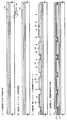
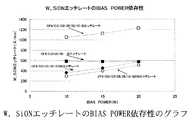
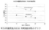
上記複数の電極に印加される高周波電力を制御する際、高周波電力における様々なパラメータ(バイアスパワー、ICPパワー、基板温度など)をそれぞれ調節することが可能であるが、ある一つのパラメータのみを調節することが望ましい。代表的には、上記複数の電極に印加される単位面積当りの高周波電力のバイアスパワー(電力パワー密度)のみをそれぞれ調節すれば、エッチング処理により得られるテーパ−角やエッチング処理のエッチングレート及び選択比の均一性を向上させることができる。なお、コイル電極(石英板の面積(直径25cmの円板))と、電極面積(12.5cm×12.5cm)とを備えたICPエッチング装置において、バイアスパワーは、図11〜図13に示すようにエッチング処理をコントロールすることができる。なお、図11にはテーパ−角のバイアスパワー依存性、図12にはW膜及びSiON膜のエッチングレートのバイアスパワー依存性、図13にはW膜とSiON膜との選択比のバイアスパワー依存性を示した。
【0018】
本明細書で開示する発明の構成(1)は、
減圧されたチャンバー内に反応ガスを供給し、第1の電極と第2の電極との間に発生するプラズマによって、前記第2の電極上に配置された基板上の被エッチング材料膜をエッチングするドライエッチング装置であって、
前記第2の電極は、各々独立した複数の電極からなり、該電極の各々に高周波電源が独立して接続されていることを特徴とするドライエッチング装置である。
【0019】
また、発明の他の構成(2)は、
減圧されたチャンバー内に反応ガスを供給し、第1の電極と第2の電極との間に交流電界を印加して発生するプラズマによって、前記第2の電極上に配置された基板上の被エッチング材料膜をエッチングするドライエッチング装置であって、前記第1の電極は平面状のコイルからなり、第1の高周波電源が接続され、
前記第2の電極は、各々独立した複数の電極からなり、該電極の各々に第2の高周波電源が独立して接続されていることを特徴とするドライエッチング装置である。
【0020】
上記構成(1)または構成(2)において、前記第2の電極を構成する複数の電極は、基板の中心部の下方に配置された電極と、基板の角部の下方に配置された電極とを有することを特徴としている。
【0021】
また、図1にその一例を示したが、前記基板の中心部の下方に配置された電極の面積は、前記基板の角部の下方に配置された電極の面積より大きいことを特徴としている。
【0022】
また、上記構成(1)または構成(2)において、図2にその一例を示したが、前記第2の電極を構成する複数の電極は、互いに同形同寸であることを特徴としている。
【0023】
また、上記各構成において、前記第2の電極を構成する複数の電極のうち、基板の中心部の下方に配置された電極に印加される高周波電力と、基板の角部の下方に配置された電極に印加される高周波電力は異なることを特徴としている。
【0024】
また、上記各構成において、前記第2の電極を構成する複数の電極のうち、基板の中心部の下方に配置された電極に印加される高周波電力の周波数と、基板の角部の下方に配置された電極に印加される高周波電力の周波数は同一であることを特徴としている。
【0025】
また、上記各構成において、前記基板は0.3m2以上の面積を有することを特徴としている。
【0026】
また、発明の他の構成(3)は、
対向する第1の電極と第2の電極とを備えたドライエッチング装置を使用するエッチング方法において、
チャンバー内に設けられた複数の電極からなる第2の電極上に基板を配置し、
減圧されたチャンバー内に反応ガスを供給し、
前記第2の電極を構成する複数の電極のうち、基板の中心部の下方に配置された電極に第1の高周波電力を印加し、基板の角部の下方に配置された電極に第2の高周波電力を印加して、前記第1の電極と前記第2の電極との間に交流電界を印加することによりプラズマを発生させて、前記複数の電極上に配置された基板上の被エッチング材料膜をエッチングすることを特徴とするエッチング方法である。
【0027】
また、上記構成(3)において、前記第1の高周波電力の周波数と前記第2の高周波電力の周波数は同一であることを特徴としている。
【0028】
また、上記構成(3)において、前記ドライエッチング装置は、平行平板型エッチング装置あるいはICP型エッチング装置である。
【0029】
また、発明の他の構成(4)は、
ドライエッチング装置を使用するエッチング方法において、
チャンバー内に設けられた複数の電極上に基板を配置し、
減圧されたチャンバー内に反応ガスを供給し、
前記複数の電極のうち、基板の中心部の下方に配置された電極に第1の高周波電力を印加し、基板の角部の下方に配置された電極に第2の高周波電力を印加し、
磁界または電界によりプラズマを発生させて、前記複数の電極上に配置された基板上の被エッチング材料膜をエッチングすることを特徴とするエッチング方法である。
【0030】
また、上記構成(4)において、前記ドライエッチング装置は、マグネトロン型エッチング装置、ECR型エッチング装置、ヘリコン型エッチング装置のいずれか一である。
【0031】
また、発明の他の構成(5)は、
基板上に導電膜を形成し、
前記導電膜上にマスクを選択的に形成し、
対向する第1の電極と第2の電極とを備えたドライエッチング装置のチャンバー内に設けられた複数の電極からなる第2の電極上に、前記基板を配置し、
減圧されたチャンバー内に反応ガスを供給し、
前記第2の電極を構成する複数の電極のうち、基板の中心部の下方に配置された電極に第1の高周波電力を印加し、基板の角部の下方に配置された電極に第2の高周波電力を印加して、前記第1の電極と前記第2の電極との間に交流電界を印加することによりプラズマを発生させて、前記複数の電極上に配置された基板上の導電膜を選択的にエッチングすることを特徴とする配線の形成方法である。
【0032】
また、上記構成(5)において、前記配線は、TFTのゲート電極またはゲート配線であることを特徴としている。なお、このゲート電極またはゲート配線の形状はテーパー形状である。
【0033】
【発明の実施の形態】
本発明の実施形態について、以下に説明する。
【0034】
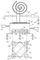
(実施の形態1)
ここではICP型エッチング装置に本発明を適用した例について説明する。なお、ICP型エッチング装置は、誘導結合プラズマを用いたエッチング装置である。
【0035】
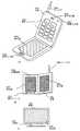
図1は、ICP型エッチング装置の断面図および上面図である。図1(B)において、エッチング装置のチャンバー101の上面は、石英ガラスなどの絶縁物100からなっており、該絶縁物100の外側に第1の電極105が配置されている。なお、図1(A)は、平面状のコイルである第1の電極105の上から見た図である。本発明において、このコイル状の第1の電極は図1に示す形状に限定されず、どのような形状のものであっても構わない。この第1の電極にはマッチング回路106を介して第1の高周波電源104が接続されている。この第1の電極105に高周波電流を流してチャンバー内に電磁波を形成し、この電磁場内に流れる電子を反応ガスの中性粒子に衝突させてプラズマを生成する。なお、反応ガスは、ガス供給系102から所定の反応ガスをチャンバー101内に導入し、ガス排気系103により排気を行う。
【0036】
被処理基板107は、複数の電極108a〜108d、109からなる第2の電極上にクランプ(図示しない)で押さえられて配置される。また、被処理基板107のサイズは、0.3m2以上の面積、例えば60cm×72cmとした場合、絶縁物100は、直径98cmの円板とすればよい。なお、図1(B)の断面図は、図1(C)に示した上面図の鎖線A−A’で切断した図に相当する。109は、被処理基板の中央部に接する第2の電極であり、108a〜108dは、被処理基板の角部に接する第2の電極である。また、各電極の間は、空隙または絶縁物でそれぞれ電気的に絶縁する。なお、電極108aには第2の高周波電源110が接続されており、電極109には第2の高周波電源111が接続されており、電極108cには第2の高周波電源112が接続されており、ここでは図示しないが電極108bや電極108dにもそれぞれ第2の高周波電源が独立に接続されている。本発明は、これらの高周波電源の高周波電力を変化させて均一なエッチングを実現するものである。また、第2の電極に印加される電力を測定する測定装置や、各高周波電源の高周波電力を制御するためのコントロール部を設けてもよい。また、第2の電極にDCパワー、ACパワー、または高周波エネルギー(マイクロ波等)を適宜、印加してエッチングを調節してもよい。
【0037】
また、図14にコントロール部601を備えたドライエッチング装置の例を示した。なお、コントロール部及び測定装置以外は図1で示したドライエッチング装置と同一であるので、同一である部分は図1の符号を用いた。図14では、プローブ600a〜600cで測定し、その値をもとにCPU等を備えたコントロール部601によって適切なバイアスパワーを算出し、各高周波電源110〜112に指示を出す。これはエッチング処理前に行って各高周波電源の出力調整を行ってもよいし、エッチング処理中に各高周波電源の出力調整を随時行ってもよい。
【0038】
次に、図1に示すエッチング装置を用いてエッチングする工程を順に説明する。
【0039】
まず、減圧されたチャンバー101内にガス供給系102から所定の反応ガスを導入しながら、ガス排気系103により排気を行い、チャンバー101内を所定の圧力に保つ。次いで、チャンバー内の圧力を保ちながら第1の高周波電源104によって高周波電力(代表的には13.56MHz)を平面状のコイルからなる第1の電極105に供給すると、チャンバー内にプラズマが発生し、第2の電極108a〜108d、109上に配置された被処理基板107に設けられた被エッチング材料膜に対してエッチングすることができる。この時、第2の電極108a〜108d、109にも第2の高周波電源110〜112によって高周波電力を供給する。ただし、各高周波電源の周波数は同一であることが好ましい。
【0040】
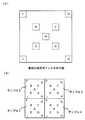
また、第2の電極の構成は、図1の構造に限定されず、少なくとも基板の角部に接する複数の電極と、基板の中央部に接する電極とを備え、それぞれに独立した高周波電源を備えていればよい。図2には、その一例を示した。第2の電極及び高周波電源以外の構造は図1に示した構造と同一であるので図1と同じ符号を用いる。図2では、第2の電極としてマトリクス状に複数の電極201が配置されており、各々の電極には独立して高周波電源202が接続されている。なお、図2(B)の断面図は、図2(C)に示した上面図の鎖線B−B’で切断した図に相当する。
【0041】
本発明により、基板全面に印加される実質的な電力パワーが均一となるように第2の電極を配置することで、基板面内のエッチングのバラツキを低減することができ、特に基板の角部におけるエッチング不良を低減することができる。また、本発明の構成であれば、大型の基板であっても面内均一性が非常に高いエッチングを実現することができる。
【0042】
また、本発明は、コイルのインダクタンスを低下させるためにコイルを分割したマルチスパイラル方式のICPエッチング装置や、くし形コイルを円状の平板に配置したスポーク形のICPエッチング装置に適用することが可能である。
【0043】
また、本発明は、ICP型エッチング装置に限定されず、RIEエッチング装置、例えば、平行平板型エッチング装置、ECRエッチング装置、マグネトロン型エッチング装置にも適用できる。
【0044】
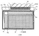
(実施の形態2)
図3には本発明を平行平板型エッチング装置に適用した一例を示した。平行平板型エッチング装置は、コンデンサを通して電極に高周波を印加することによって生成される容量結合プラズマを用いたエッチング装置である。
【0045】
305はアースに接続された第1の電極(上部電極)であり、この第1の電極305と第2の電極との間に高周波電界を印加してチャンバー301内の反応ガスをイオン化させ、反応ガス中のイオンにより被処理基板307上に設けられた被エッチング材料膜をエッチングする。なお、反応ガスは、ガス供給系302から所定の反応ガスをチャンバー301内に導入し、ガス排気系303により排気を行う。
【0046】
また、被処理基板307は複数の電極308a〜308d、309からなる第2の電極(下部電極)上に石英等からなる絶縁物300を介して配置する。なお、被処理基板の角部の下方に配置された電極308aには第2の高周波電源310が接続されており、被処理基板の中央部の下方に配置された電極309には第2の高周波電源311が接続されており、電極308cには第2の高周波電源312が接続されており、ここでは図示しないが電極308bや電極308dにもそれぞれ第2の高周波電源が独立に接続されている。なお、図3(A)の断面図は、図3(B)に示した上面図の鎖線A−A’で切断した図に相当する。このように、図3に示す平行平板型エッチング装置においても、第2の電極を構成する複数の電極の各々に独立して高周波電源310〜312を接続している。
【0047】
上記構成により、基板全面に印加される実質的な電力パワーが均一となるように第2の電極を配置することで、基板面内のエッチングのバラツキを低減することができ、特に基板の角部におけるエッチング不良を低減することができる。また、上記構成の構成であれば、大型の基板であっても面内均一性が非常に高いエッチングを実現することができる。
【0048】
また、第2の電極と第2の高周波電源の間に測定装置(プロ−バー、電圧測定機器、オシロスコープ等)313が設けられている。さらに、この測定装置313から得られた情報をもとにして、各高周波電源の高周波電力を制御するためのコントロール部を設けてもよい。
【0049】
なお、図3では第2の電極上に石英等からなる絶縁物を介して被処理基板を配置した例を示したが、第2の電極と接して被処理基板を配置してもよい。
【0050】
以上の構成でなる本発明について、以下に示す実施例でもってさらに詳細な説明を行うこととする。
【0051】
【実施例】
[実施例1]
本実施例は、同一基板上に画素部と駆動回路とを備えた液晶表示装置の作製方法の一例を図4〜図8を用いて示す。
【0052】
まず、本実施例ではコーニング社の#7059ガラスや#1737ガラスなどに代表されるバリウムホウケイ酸ガラス、またはアルミノホウケイ酸ガラスなどのガラスからなる基板401を用いる。なお、基板401としては、透光性を有する基板であれば限定されず、石英基板を用いても良い。また、本実施例の処理温度に耐えうる耐熱性が有するプラスチック基板を用いてもよい。
【0053】
次いで、基板401上に酸化シリコン膜、窒化シリコン膜または酸化窒化シリコン膜などの絶縁膜から成る下地膜402を形成する。
【0054】
下地絶縁膜402としては、酸化シリコン膜、窒化シリコン膜、窒化酸化シリコン膜(SiOx Ny )、またはこれらの積層膜等を100〜500nmの膜厚範囲で用いることができ、形成手段としては公知の成膜方法(熱CVD法、プラズマCVD法、蒸着法、スパッタ法、減圧熱CVD法等)を用いる。ここでは、膜組成において酸素元素より窒素元素を多く含む酸化窒化シリコン膜402aと、膜組成において窒素元素より酸素元素を多く含む酸化窒化シリコン膜402bを積層形成した。
【0055】
次いで、下地絶縁膜上に非晶質半導体膜403を形成する。(図4(A))非晶質半導体膜の材料に限定はないが、好ましくはシリコンまたはシリコンゲルマニウム(SiXGe1-X(0<X<1))合金などで形成すると良い。形成手段としては公知の成膜方法(熱CVD法、プラズマCVD法、蒸着法、スパッタ法、減圧熱CVD法等)を用いることができる。
【0056】
次いで、非晶質半導体膜403を結晶化させて結晶質半導体膜404を形成する。(図4(B))結晶化方法は公知の方法(固相成長法、レーザー結晶化法、結晶化を助長する金属元素を用いた固相成長法等)を用いることができる。本実施例では、レーザー結晶化法により結晶質シリコン膜を形成した。レーザー結晶化法で結晶質半導体膜を作製する場合には、パルス発振型または連続発振型のエキシマレーザーや、パルス発振型または連続発振型のYAGレーザーや、YVO4レーザーを用いることができる。
【0057】
次いで、フォトリソグラフィ法によりレジストマスクを形成し、エッチングを行って所望の形状の半導体層405〜409を形成する。ここで、実施の形態1または実施の形態2に記載のドライエッチング装置を用いれば、面内均一性の優れたエッチングを行うことができる。
【0058】
次いで、保護膜410を介してp型を付与する不純物元素(以下、p型不純物元素という)を添加する。(図4(C))p型不純物元素としては、代表的には13族に属する元素、典型的にはボロンまたはガリウムを用いることができる。この工程(チャネルドープ工程という)はTFTのしきい値電圧を制御するための工程である。なお、ここではジボラン(B2H6)を質量分離しないでプラズマ励起したイオンドープ法でボロンを添加する。勿論、質量分離を行うイオンインプランテーション法を用いても良い。
【0059】
なお、本実施例ではチャネルドープ工程を行ったが、特に必要でない場合には行わなくても構わない。
【0060】
次いで、保護膜410を除去した後、ゲート絶縁膜となる絶縁膜411(ここでは酸化窒化シリコン膜)を半導体層上に成膜し、さらにその上に第1導電膜412及び第2導電膜413を積層形成する。(図4(D))
【0061】
次に図5(A)に示すように、フォトリソグラフィ法によりレジストによるマスク414を形成し、ゲート電極を形成するための第1のエッチング処理を行う。エッチング方法に限定はないが、好適には本発明のICP(Inductively Coupled Plasma:誘導結合型プラズマ)エッチング法を用いる。エッチング用ガスにCF4とCl2を混合し、0.5〜2Pa、好ましくは1Paの圧力でコイル型の電極に500W(電力パワー密度1.02W/cm2)のRF(13.56MHz)電力を投入してプラズマを生成して行う。なお、基板側の電極面積サイズは、12.5cm×12.5cmであり、コイル型の電極面積サイズ(ここではコイルの設けられた石英円板)は、直径25cmの円板である。基板側(試料ステージ)にも100W(電力パワー密度0.64W/cm2)のRF(13.56MHz)電力を投入し、実質的に負の自己バイアス電圧を印加する。CF4とCl2を混合した場合にはタングステン膜、窒化タンタル膜及びチタン膜の場合でも、それぞれ同程度の速度でエッチングすることができる。
【0062】
上記エッチング条件では、レジストによるマスクの形状と、基板側に印加するバイアス電圧の効果により端部をテーパー形状とすることができる。テーパー部の角度は15〜45°となるようにする。なお、図11に上記エッチング条件(圧力1Pa、500WのRF電力、ガス流量CF4/Cl2=30sccm/30sccm)でのバイアスパワーの依存性のグラフを示した。また、ゲート絶縁膜上に残渣を残すことなくエッチングするためには、10〜20%程度の割合でエッチング時間を増加させると良い。W膜に対する酸化窒化シリコン膜の選択比は2〜4(代表的には3)であるので、オーバーエッチング処理により、酸化窒化シリコン膜が露出した面は20〜50nm程度エッチングされる。また、図12はW膜及び酸化窒化シリコン膜のエッチングレートのバイアスパワー依存性を示すグラフ、図13は、W膜に対する酸化窒化シリコン膜の選択比のバイアスパワー依存性を示すグラフである。
【0063】
本実施例では、この第1のエッチング処理を実施の形態1に示した本発明のドライエッチング装置(図1または図2)及びエッチング方法を用いて行う。本発明のドライエッチング装置を用いることによってテーパ−部の角度(テーパー角)が均一化できる。ここでは、第2の電極の電極サイズを考慮し、図11を元にして第2の電極に印加されるバイアスパワーをそれぞれ調節して電力パワー密度を均一化させ、基板面内のテーパー角を均一化した。後の工程でこのテーパ−部を通過させて低濃度不純物領域を形成するため、このテーパ−部を均一にすることは、結果的に基板面内に形成される全てのTFTの電気的特性を均一化することにつながる。従って、本発明のエッチング装置を用いることは、基板面内のバラツキ低減に極めて有用である。
【0064】
こうして、第1のエッチング処理により第1導電膜と第2導電膜から成る第1形状の導電層415〜420(第1の導電層415a、416a、417a、418a、419a、420aと第2導電層415b、416b、417b、418b、419b、420b)を形成する。なお、図示しないが、絶縁膜413において、第1の形状の導電層で覆われない領域は20〜50nm程度エッチングされ薄くなる。
【0065】
次いで、レジストマスクをそのままの状態としたまま、第1の形状の導電層をマスクとして第1のドーピング処理を行いn型の不純物(ドナー)をドーピングする。(図5(B))例えば、加速電圧を20〜60keVとし、1×10¹³〜5×10¹⁴/cm2のドーズ量で行い、不純物領域(n+領域)421a〜421eを形成する。例えば、不純物領域(n+領域)におけるリン(P)濃度は1×1020〜1×1021/cm3の範囲となるようにする。
【0066】
次いで、レジストマスクをそのままの状態としたまま、図5(C)に示すように第2のエッチング処理を行う。エッチングはICPエッチング法を用い、エッチングガスにCF4とCl2とO2を混合して、1Paの圧力でコイル型の電極に500W(電力パワー密度1.02W/cm2)のRF電力(13.56MHz)を供給してプラズマを生成する。基板側(試料ステージ)には50W(電力パワー密度0.32W/cm2)のRF(13.56MHz)電力を投入し、第1のエッチング処理に比べ低い自己バイアス電圧を印加する。このような条件によりタングステン膜を異方性エッチングし、第1の導電層である窒化タンタル膜またはチタン膜を残存させるようにする。ここでも本発明のICP型エッチング装置を用いて面内均一性を向上させることが望ましい。こうして、第2形状の導電層423〜428(第1の導電膜423a、424a、425a、426a、427a、428aと第2の導電膜423b、424b、425b、426b、427b、428b)を形成する。422はゲート絶縁膜であり、第2の形状の導電層で覆われない領域はさらに薄くなった。
【0067】
次いで、レジストマスクをそのままの状態としたまま、第2のドーピング処理を行いn型の不純物(ドナー)をドーピングする。(図5(D))この場合、第2形状の導電層のうち、第2の導電膜はドーピングする元素に対してマスクとなり、加速電圧を適宣調節(例えば、70〜120keV)して、ゲート絶縁膜及び第1の導電膜のテーパ部を通過した不純物元素により不純物領域(n−領域)429a〜429eを形成する。例えば、不純物領域(n−領域)におけるリン(P)濃度は1×10¹⁷〜1×10¹⁹/cm3の範囲となるようにする。
【0068】
本実施例では、本発明のICP型エッチング装置を用いたことによって、テーパ部が均一化されたため、テーパ部を通過させて形成される不純物領域(n−領域)を基板面内において均一化することができた。
【0069】
次いで、レジストマスクを除去した後、フォトリソグラフィ法により、駆動回路のnチャネルTFTのうち、所定のTFTを覆うレジストマスク430を形成した後、エッチングを行い、第3形状の導電層(第1の導電膜423c、425c、426c、427c、428cと第2の導電膜423d、425d、426d、427d、428d)と絶縁膜431〜436を形成する。(図6(A))こうすることによって、レジストマスク430で覆われたTFT以外のTFTは、第1の導電膜と不純物領域(n−領域)とが重ならないTFTとすることができる。なお、図6(A)中では絶縁膜431、433〜436が不純物領域(n−領域)と重なっていないが、実際は、一部かさなった構造となる。
【0070】
次いで、レジストマスク430を除去した後、図6(B)に示すように、レジストによるマスク437を形成し、pチャネル型TFTを形成する島状半導体層にp型の不純物(アクセプタ)をドーピングする。典型的にはボロン(B)を用いる。不純物領域(p+領域)438、439の不純物濃度は2×10²⁰〜2×10²¹/cm3となるようにし、含有するリン濃度の1.5〜3倍のボロンを添加して導電型を反転させる。
【0071】
以上までの工程でそれぞれの半導体層に不純物領域が形成される。その後、図6(C)に示すように、窒化シリコン膜または酸化窒化シリコン膜から成る保護絶縁膜440をプラズマCVD法で形成する。そして導電型の制御を目的としてそれぞれの半導体層に添加された不純物元素を活性化する工程を行う。
【0072】
さらに、水素化処理を行う。本実施例では比較的低温で行うことが可能な水素プラズマを用いて水素化処理を行った。
【0073】
次いで、保護絶縁膜440を覆って層間絶縁膜441を形成する。層間絶縁膜441は、ポリイミド、アクリルなどの有機絶縁物材料で形成する。勿論、プラズマCVD法でTEOS(Tetraethyl Ortho silicate)を用いて形成される酸化シリコン膜を適用しても良いが、平坦性を高める観点からは前記有機物材料を用いることが望ましい。
【0074】
次いで、コンタクトホールを形成し、アルミニウム(Al)またはAgを主成分とする膜、チタン(Ti)、またはそれらの積層膜等の反射性の優れた材料を用いて、ソース配線またはドレイン配線442〜450、及び画素電極451を形成する。また、画素電極451を形成した後、公知のサンドブラスト法やエッチング法等の工程を追加して表面を凹凸化させて、鏡面反射を防ぎ、反射光を散乱させることによって白色度を増加させることが好ましい。
【0075】
以上の工程で、nチャネル型TFTとpチャネル型TFTと含む駆動回路453と、画素TFT及び保持容量を含む画素部454を同一基板上に得ることができる。
【0076】
駆動回路453において、ロジック回路部やサンプリング回路部を構成するpチャネル型TFTにはチャネル形成領域、ソース領域またはドレイン領域として機能する不純物領域を有している。
【0077】
駆動回路453において、ロジック回路部を構成するnチャネル型TFTには高速動作を重視したTFT構造とすることが好ましく、チャネル形成領域、ゲート電極と重なる不純物領域(Gate Overlapped Drain:GOLD領域)、ゲート電極の外側に形成される不純物領域(LDD領域)とソース領域またはドレイン領域として機能する不純物領域を有している。
【0078】
また、駆動回路453において、サンプリング回路部を構成するnチャネル型TFTには低オフ電流動作を重視したTFT構造とすることが好ましく、チャネル形成領域、ゲート電極の外側に形成される不純物領域(LDD領域)とソース領域またはドレイン領域として機能する不純物領域を有している。
【0079】
また、画素部454の画素TFTを構成するnチャネル型TFTには低オフ電流動作を重視したTFT構造とすることが好ましく、チャネル形成領域、ゲート電極の外側に形成される不純物領域(LDD領域)とソース領域またはドレイン領域として機能する不純物領域を有している。
【0080】
また、画素部454の保持容量460の一方の電極として機能する半導体層には、それぞれp型を付与する不純物元素が添加されている。保持容量460は、絶縁膜436を誘電体として、電極428d、428cと、半導体層とで形成している。
【0081】
なお、ここでは、画素電極として、反射電極を用いた例を示したが、透光性を有する導電性材料を用いて画素電極を形成すれば、透過型の表示装置を作製することができる。その場合、ソース配線またはドレイン配線を作製する工程の前後で画素電極を形成し、その画素電極の材料としては、酸化インジウム酸化亜鉛合金(In2O3―ZnO)、酸化亜鉛(ZnO)、またはガリウム(Ga)を添加した酸化亜鉛(ZnO:Ga)等を用いることが望ましい。
【0082】
図7の状態を得た後、画素電極451上に配向膜を形成しラビング処理を行う。なお、本実施例では配向膜を形成する前に、アクリル樹脂膜等の有機樹脂膜をパターニングすることによって基板間隔を保持するための柱状のスペーサ(図示しない)を所望の位置に形成した。また、柱状のスペーサに代えて、球状のスペーサを基板全面に散布してもよい。
【0083】
次いで、対向基板を用意する。次いで、対向基板上に着色層、遮光層を形成した後、平坦化膜を形成する。次いで、平坦化膜上に透明導電膜からなる対向電極を少なくとも画素部に形成し、対向基板の全面に配向膜を形成し、ラビング処理を施した。
【0084】
次いで、画素部と駆動回路が形成された基板と対向基板とを接着層(本実施例ではシール材)で貼り合わせる。接着層にはフィラーが混入されていて、このフィラーと柱状スペーサによって均一な間隔を持って2枚の基板が貼り合わせられる。そして、一枚の基板に複数の画素部を形成、いわゆる多面取りとした場合、基板を各々分断して、一つの画素部を有する基板を複数得る。その後、両基板の間に液晶材料を注入し、封止剤(図示せず)によって完全に封止する。液晶材料には公知の液晶材料を用いれば良い。
【0085】
次いで、外部入力端子にFPC(フレキシブルプリント配線板:Flexible Printed Circuit)を貼り付ける。さらに対向基板のみに偏光板(図示しない)を貼りつける。また、カラー化させる場合にはカラーフィルタを基板に設ける。
【0086】
以上のようにして作製される液晶表示装置は各種電子機器の表示部として用いることができる。この液晶表示装置の状態について図8を用いて説明する。
【0087】
図8に示す上面図は、画素部、駆動回路、FPC89(フレキシブルプリント配線板:Flexible Printed Circuit)を貼り付ける外部入力端子80、外部入力端子と各回路の入力部までを接続する配線81などが形成された基板82aと、カラーフィルタなどが設けられた対向基板82bとがシール材83を介して貼り合わされている。
【0088】
ゲート側駆動回路84と重なるように固定基板側に遮光層86aが設けられ、ソース側駆動回路85と重なるように固定基板側に遮光層86bが形成されている。また、画素部87上の固定基板側に設けられたカラーフィルタ88は遮光層と、赤色(R)、緑色(G)、青色(B)の各色の着色層とが各画素に対応して設けられている。実際に表示する際には、赤色(R)の着色層、緑色(G)の着色層、青色(B)の着色層の3色でカラー表示を形成するが、これら各色の着色層の配列は任意なものとする。
【0089】
ここでは、カラー化を図るためにカラーフィルタ88を対向基板に設けているが特に限定されず、基板上に素子を作製する際、基板上にカラーフィルタを形成してもよい。
【0090】
また、カラーフィルタにおいて隣り合う画素の間には遮光層が設けられており、表示領域以外の箇所を遮光している。また、ここでは、駆動回路を覆う領域にも遮光層86a、86bを設けているが、駆動回路を覆う領域は、後に液晶表示装置を電子機器の表示部として組み込む際、カバーで覆うため、特に遮光層を設けない構成としてもよい。また、基板上に必要な素子を作製する際、基板上に遮光層を形成してもよい。
【0091】
また、上記遮光層を設けずに、第2固定基板と対向電極の間に、カラーフィルタを構成する着色層を複数層重ねた積層で遮光するように適宜配置し、表示領域以外の箇所(各画素電極の間隙)や、駆動回路を遮光してもよい。
【0092】
また、外部入力端子にはベースフィルムと配線から成るFPC89が異方性導電性樹脂で貼り合わされている。さらに補強板で機械的強度を高めている。
【0093】
[実施例2]
本実施例では、画素部または駆動回路に使用するTFTを逆スタガ型TFTで構成した液晶表示装置の例を図9に示す。図9(A)は、画素部の画素の一つを拡大した上面図であり、図9(A)において、点線A−A'で切断した部分が、図9(B)の画素部の断面構造に相当する。
【0094】
画素部において、画素TFT部はNチャネル型TFTで形成されている。なお、TFTの活性層は、非晶質構造を有する半導体膜(代表的にはアモルファスシリコン膜)や結晶構造を有する半導体膜(代表的にはポリシリコン膜)のいずれでもよいが、駆動回路と画素部とを同一基板上に形成する場合には、結晶構造を有する半導体膜を用いることが望ましい。基板上51にゲート電極52が形成され、その上に窒化珪素からなる第1絶縁膜53a、酸化珪素からなる第2絶縁膜53bが設けられている。なお、53a、53bはゲート絶縁膜としての機能を有する。また、第2絶縁膜53b上には、活性層としてn+ 領域54〜56と、チャネル形成領域57、58と、前記n+ 型領域とチャネル形成領域の間にn- 型領域59、60が形成される。また、チャネル形成領域57、58は絶縁層61、62で保護される。絶縁層61、62及び活性層を覆う第1の層間絶縁膜63にコンタクトホールを形成した後、n+ 領域54に接続する配線64が形成され、n+ 領域56にAlあるいはAg等からなる画素電極65が接続され、さらにその上にパッシベーション膜66が形成される。また、70は画素電極65と隣接する画素電極である。
【0095】
なお、本実施例では、画素部の画素TFTのゲート配線をダブルゲート構造としているが、オフ電流のバラツキを低減するために、トリプルゲート構造等のマルチゲート構造としても構わない。また、開口率を向上させるためにシングルゲート構造としてもよい。
【0096】
また、画素部の容量部は、第1絶縁膜及び第2絶縁膜を誘電体として、容量配線71と、n+ 領域56とで形成されている。
【0097】
なお、図9で示した画素部はあくまで一例に過ぎず、特に上記構成に限定されないことはいうまでもない。
【0098】
また、本実施例は、実施の形態1、実施の形態2、実施例1のいずれとも自由に組み合わせることが可能である。
【0099】
実施の形態1や実施の形態2にその一例を示した本発明のエッチング装置は、各パターニング工程でのエッチング処理に適用することができるが、特にゲート電極52のパターニングにおけるエッチング処理に用いて、ゲート電極52のテーパ部を均一とし、そのゲート電極52を覆うゲート絶縁膜のカバレッジを良好なものとすることができる。本発明により、被処理基板が大型化しても被処理基板の角部におけるエッチング不良を引き起こすことなく、面内均一性に優れ、且つ、精度の高いエッチング処理を行うことができる。
【0100】
[実施例3]
本実施例では、EL(Electro Luminescence)素子を備えた自発光表示装置を作製する例を図10に示す。
【0101】
図10(A)は、ELモジュールをを示す上面図、図10(B)は図1(A)をA−A’で切断した断面図である。絶縁表面を有する基板500(例えば、ガラス基板、結晶化ガラス基板、もしくはプラスチック基板等)に、画素部502、ソース側駆動回路501、及びゲート側駆動回路503を形成する。また、518はシール材、519はDLC膜であり、画素部および駆動回路部はシール材518で覆われ、そのシール材は保護膜519で覆われている。さらに、接着材を用いてカバー材で封止されている。
【0102】
なお、508はソース側駆動回路501及びゲート側駆動回路503に入力される信号を伝送するための配線であり、外部入力端子となるFPC(フレキシブルプリントサーキット)509からビデオ信号やクロック信号を受け取る。なお、ここではFPCしか図示されていないが、このFPCにはプリント配線基盤(PWB)が取り付けられていても良い。本明細書における自発光装置には、自発光装置本体だけでなく、それにFPCもしくはPWBが取り付けられた状態をも含むものとする。
【0103】
次に、断面構造について図10(B)を用いて説明する。基板500上に絶縁膜510が設けられ、絶縁膜510の上方には画素部502、ゲート側駆動回路503が形成されており、画素部502は電流制御用TFT511とそのドレインに電気的に接続された画素電極512を含む複数の画素により形成される。また、ゲート側駆動回路503はnチャネル型TFT513とpチャネル型TFT514とを組み合わせたCMOS回路を用いて形成される。
【0104】
これらのTFT(511、513、514を含む)を作製する際のパターニングにおいて、本発明のエッチング装置を用いれば、面内均一性の高い半導体層の形状、配線幅、またはコンタクトホール形状を実現することができる。
【0105】
画素電極512はEL素子の陽極として機能する。また、画素電極512の両端にはバンク515が形成され、画素電極512上にはEL層516およびEL素子の陰極517が形成される。
【0106】
EL層516としては、発光層、電荷輸送層または電荷注入層を自由に組み合わせてEL層(発光及びそのためのキャリアの移動を行わせるための層)を形成すれば良い。例えば、低分子系有機EL材料や高分子系有機EL材料を用いればよい。また、EL層として一重項励起により発光(蛍光)する発光材料(シングレット化合物)からなる薄膜、または三重項励起により発光(リン光)する発光材料(トリプレット化合物)からなる薄膜を用いることができる。また、電荷輸送層や電荷注入層として炭化珪素等の無機材料を用いることも可能である。これらの有機EL材料や無機材料は公知の材料を用いることができる。
【0107】
陰極517は全画素に共通の配線としても機能し、接続配線508を経由してFPC509に電気的に接続されている。さらに、画素部502及びゲート側駆動回路503に含まれる素子は全て陰極517、シール材518、及び保護膜519で覆われている。
【0108】
なお、シール材518としては、できるだけ可視光に対して透明もしくは半透明な材料を用いるのが好ましい。また、シール材518はできるだけ水分や酸素を透過しない材料であることが望ましい。
【0109】
また、シール材518を用いて発光素子を完全に覆った後、すくなくとも図10に示すようにDLC膜等からなる保護膜519をシール材518の表面(露呈面)に設けることが好ましい。また、基板の裏面を含む全面に保護膜を設けてもよい。ここで、外部入力端子(FPC)が設けられる部分に保護膜が成膜されないように注意することが必要である。マスクを用いて保護膜が成膜されないようにしてもよいし、CVD装置でマスキングテープとして用いるテフロン(登録商標)等のテープで外部入力端子部分を覆うことで保護膜が成膜されないようにしてもよい。
【0110】
以上のような構造でEL素子をシール材518及び保護膜で封入することにより、EL素子を外部から完全に遮断することができ、外部から水分や酸素等のEL層の酸化による劣化を促す物質が侵入することを防ぐことができる。従って、信頼性の高い自発光装置を得ることができる。
【0111】
また、本実施例は、実施の形態1、実施の形態2、実施例1、実施例2のいずれとも自由に組み合わせることが可能である。
【0112】
実施の形態1や実施の形態2にその一例を示した本発明は、図10に示す画素部のTFTあるいは駆動回路のTFTを作製する際に使用するエッチング処理(電極形成、コンタクトホールの形成など)に適用することができる。本発明により、被処理基板が大型化しても被処理基板の角部におけるエッチング不良を引き起こすことなく、面内均一性に優れ、且つ、精度の高いエッチング処理を行うことができる。
【0113】
また、画素電極を陰極とし、EL層と陽極を積層して図10とは逆方向に発光する構成としてもよい。
【0114】
[実施例4]
本実施例は、本発明を適用し、ラジアルラインスロットアンテナ(RLSA)をマイクロ波供給手段として用いたエッチング装置の一例を図15に示す。
【0115】
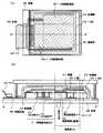
図15中、700はラジアルラインスロットアンテナ(RLSA)であり、704はマイクロ波透過性の誘電体であり、このアンテナ700からマイクロ波を供給してアンテナ700と電極708、709との間にプラズマを発生させ、被処理基板707上に設けられた被エッチング材料膜をエッチングする。なお、反応ガスは、ガス供給系702から所定の反応ガスをチャンバー701内に導入し、ガス排気系703により排気を行う。
【0116】
また、被処理基板707は複数の電極708a〜708d、709からなる第2の電極(下部電極)上に配置する。なお、被処理基板の角部の下方に配置された電極708aには高周波電源710が接続されており、被処理基板の中央部の下方に配置された電極709には高周波電源711が接続されており、電極708cには高周波電源712が接続されており、ここでは図示しないが電極708bや電極708dにもそれぞれ高周波電源が独立に接続されている。なお、図15(A)の断面図は、図15(B)に示した上面図の鎖線A−A’で切断した図に相当する。このように、図15に示すエッチング装置においても、電極を構成する複数の電極の各々に独立して高周波電源710〜712を接続している。
【0117】
上記構成により、基板面内のエッチングのバラツキを低減することができ、特に基板の角部におけるエッチング不良を低減することができる。また、上記構成の構成であれば、大型の基板であっても面内均一性が非常に高いエッチングを実現することができる。
【0118】
また、電極と高周波電源の間に測定装置(プロ−バー、電圧測定機器、オシロスコープ等)を設けてもよい。さらに、この測定装置から得られた情報をもとにして、各高周波電源の高周波電力を制御するためのコントロール部を設けてもよい。
【0119】
また、本実施例は、実施の形態1、実施の形態2、実施例1、実施例2、実施例3のいずれとも自由に組み合わせることが可能である。
【0120】
[実施例5]
本実施例では、画素部に使用するnチャネル型TFTの下方に遮光膜を兼ねるゲート配線を設けた液晶表示装置の例を図16に示す。図16(B)は、画素部の画素の一つを拡大した上面図であり、図16(B)において、点線E−E'で切断した部分が、図16(A)の画素部の断面構造に相当する。
【0121】
図16において、801は基板、802はゲート配線、803a、803bはゲート配線を覆う絶縁膜、808はゲート絶縁膜、810はゲート電極、811は容量配線である。なお、このゲート配線802は活性層を光から保護する遮光層としても機能する。また、活性層は、812〜815で示す領域からなり、そのうち812は、LDD領域となる低濃度不純物領域、813は、高濃度にリンが添加されたソース領域またはドレイン領域となる高濃度不純物領域、814、815はチャネル形成領域である。なお、低濃度不純物領域812は、セルフアラインでドーピングされており、ゲート電極810とは重なっていない。
【0122】
また、図16(A)において、816は、パッシベーション膜、817は有機樹脂材料からなる層間絶縁膜、818は画素電極と高濃度不純物領域を接続する電極、819はソース配線、820はアクリルからなる層間絶縁膜、821は遮光層、822は層間絶縁膜、823、824は透明導電膜からなる画素電極である。
【0123】
本発明は、図16に示す画素TFTを作製する際に使用するエッチング処理に適用することができる。
【0124】
また、図17に、図16とはゲート電極と活性層の構成が異なる例を示した。なお、図17は図16とはゲート電極と活性層の構成が異なるだけで、それら以外の構成は図16と同一であるので説明を省略する。
【0125】
図17中、活性層は、高濃度不純物領域913、低濃度不純物領域912、チャネル形成領域914、915からなる。 図17ではゲート電極910及び容量配線911の形状がテーパ−形状となっており、ドーピングの際、このテーパ−部を通過させてリンをドーピングし、低濃度不純物領域912を形成した。従って、低濃度不純物領域912は、ゲート電極910とは一部重なっている。
【0126】
また、本実施例は、実施の形態1、実施の形態2、実施例1、実施例2、実施例3のいずれとも自由に組み合わせることが可能である。
【0127】
実施の形態1や実施の形態2にその一例を示した本発明は、図16に示す画素TFTを作製する際、例えばテーパ−形状のゲート電極の形成に使用するエッチング処理、コンタクトホール形成に使用するエッチング処理に適用することができる。本発明により、被処理基板が大型化しても被処理基板の角部におけるエッチング不良を引き起こすことなく、面内均一性に優れ、且つ、精度の高いエッチング処理を行うことができる。
【0128】
[実施例6]
本発明を実施して形成された駆動回路や画素部は様々な装置(アクティブマトリクス型液晶ディスプレイ、アクティブマトリクス型ELモジュール、アクティブマトリクス型ECディスプレイなど)に用いることができる。本発明は、駆動回路や画素部に設けるTFTを作製する際、例えばテーパ−形状のゲート電極の形成に使用するエッチング処理、コンタクトホール形成に使用するエッチング処理に適用することができる。即ち、それらの装置を含む電子機器全てに本発明を実施できる。
【0129】
その様な電子機器としては、ビデオカメラ、デジタルカメラ、ヘッドマウントディスプレイ(ゴーグル型ディスプレイ)、カーナビゲーション、プロジェクタ、カーステレオ、パーソナルコンピュータ、携帯情報端末(モバイルコンピュータ、携帯電話または電子書籍等)などが挙げられる。それらの一例を図18〜図20に示す。
【0130】
図18(A)はパーソナルコンピュータであり、本体2001、画像入力部2002、表示部2003、キーボード2004等を含む。
【0131】
図18(B)はビデオカメラであり、本体2101、表示部2102、音声入力部2103、操作スイッチ2104、バッテリー2105、受像部2106等を含む。
【0132】
図18(C)はモバイルコンピュータ(モービルコンピュータ)であり、本体2201、カメラ部2202、受像部2203、操作スイッチ2204、表示部2205等を含む。
【0133】
図18(D)はゴーグル型ディスプレイであり、本体2301、表示部2302、アーム部2303等を含む。
【0134】
図18(E)はプログラムを記録した記録媒体(以下、記録媒体と呼ぶ)を用いるプレーヤーであり、本体2401、表示部2402、スピーカ部2403、記録媒体2404、操作スイッチ2405等を含む。なお、このプレーヤーは記録媒体としてDVD(Digtial Versatile Disc)、CD等を用い、音楽鑑賞や映画鑑賞やゲームやインターネットを行うことができる。
【0135】
図18(F)はデジタルカメラであり、本体2501、表示部2502、接眼部2503、操作スイッチ2504、受像部(図示しない)等を含む。
【0136】
図19(A)はフロント型プロジェクターであり、投射装置2601、スクリーン2602等を含む。
【0137】
図19(B)はリア型プロジェクターであり、本体2701、投射装置2702、ミラー2703、スクリーン2704等を含む。
【0138】
なお、図19(C)は、図19(A)及び図19(B)中における投射装置2601、2702の構造の一例を示した図である。投射装置2601、2702は、光源光学系2801、ミラー2802、2804〜2806、ダイクロイックミラー2803、プリズム2807、液晶表示装置2808、位相差板2809、投射光学系2810で構成される。投射光学系2810は、投射レンズを含む光学系で構成される。本実施例は三板式の例を示したが、特に限定されず、例えば単板式であってもよい。また、図19(C)中において矢印で示した光路に実施者が適宜、光学レンズや、偏光機能を有するフィルムや、位相差を調節するためのフィルム、IRフィルム等の光学系を設けてもよい。
【0139】
また、図19(D)は、図19(C)中における光源光学系2801の構造の一例を示した図である。本実施例では、光源光学系2801は、リフレクター2811、光源2812、レンズアレイ2813、2814、偏光変換素子2815、集光レンズ2816で構成される。なお、図19(D)に示した光源光学系は一例であって特に限定されない。例えば、光源光学系に実施者が適宜、光学レンズや、偏光機能を有するフィルムや、位相差を調節するフィルム、IRフィルム等の光学系を設けてもよい。
【0140】
ただし、図19に示したプロジェクターにおいては、透過型の電気光学装置を用いた場合を示しており、反射型の電気光学装置及びELモジュールでの適用例は図示していない。
【0141】
図20(A)は携帯電話であり、本体2901、音声出力部2902、音声入力部2903、表示部2904、操作スイッチ2905、アンテナ2906、画像入力部(CCD、イメージセンサ等)2907等を含む。
【0142】
図20(B)は携帯書籍(電子書籍)であり、本体3001、表示部3002、3003、記憶媒体3004、操作スイッチ3005、アンテナ3006等を含む。
【0143】
図20(C)はディスプレイであり、本体3101、支持台3102、表示部3103等を含む。本発明は特に大画面化した場合において有利であり、対角10インチ以上(特に30インチ以上)のディスプレイには有利である。
【0144】
以上の様に、本発明の適用範囲は極めて広く、あらゆる分野の電子機器の作製方法に適用することが可能である。また、本実施例の電子機器は実施例1〜5のどのような組み合わせからなる構成を用いても実現することができる。
【0145】
【発明の効果】
本発明により、被処理基板が大型化しても被処理基板内におけるエッチング不良を引き起こすことなく、面内均一性に優れ、且つ、精度の高いエッチング処理を行うことができる。従って、本発明のドライエッチング装置は、大型の量産装置に適している。
【0146】
また、本発明により、膜厚が薄い被処理膜をエッチングする場合や、選択比が低いエッチング処理を行う場合において、従来生じていた部分的なオーバーエッチングを抑えることができ、有効である。
【0147】
また、本発明により、被処理基板が大型化しても基板全面に渡って、半導体層の形状やコンタクトホールの形状を均一化することができる。
【0148】
また、エッチングによって配線のテーパ部のテーパ−角を制御する場合において、本発明により基板全体に均一なテーパ−角を得ることができ、特に有効である。
【図面の簡単な説明】
【図1】 本発明のドライエッチング装置の構成を示す図である。
【図2】 本発明のドライエッチング装置の構成を示す図である。
【図3】 本発明のドライエッチング装置の構成を示す図である。
【図4】 AM−LCDの作製工程を示す図である。
【図5】 AM−LCDの作製工程を示す図である。
【図6】 AM−LCDの作製工程を示す図である。
【図7】 アクティブマトリクス型液晶表示装置の断面構造図を示す図である。
【図8】 AM−LCDの外観を示す図である。
【図9】 アクティブマトリクス型液晶表示装置の画素上面図および画素断面図を示す図である。
【図10】 アクティブマトリクス型EL表示装置の外観図および断面図を示す図である。
【図11】 テーパ−角αのバイアスパワー依存性を示す図である。
【図12】 エッチングレートのバイアスパワー依存性を示す図である。
【図13】 選択比のバイアスパワー依存性を示す図である。
【図14】 コントロール部を備えたドライエッチング装置を示す図である。
【図15】 本発明のドライエッチング装置の構成を示す図である。
【図16】 アクティブマトリクス型液晶表示装置の画素上面図及び断面図を示す図である。
【図17】 アクティブマトリクス型液晶表示装置の画素断面図を示す図である。
【図18】 電子機器の一例を示す図。
【図19】 電子機器の一例を示す図。
【図20】 電子機器の一例を示す図。
【図21】 基板の測定ポイントを示す図。[0001]
BACKGROUND OF THE INVENTION
The present invention relates to a dry etching apparatus, and more particularly to an etching apparatus and an etching method using plasma generated by applying a magnetic field or an electric field to a reaction gas introduced into a reduced pressure chamber.
[0002]
[Prior art]
Conventionally, the processing capacity of the dry etching apparatus is limited, and there is a problem in terms of improving productivity.
[0003]
In order to improve the production efficiency, the size of the mother glass is increasing year by year. As a large substrate used at present, a size of 550 mm × 650 mm or a size of 650 mm × 830 mm is used. In the future, it is expected that a size of 850 mm × 950 mm or a size of 950 mm × 1000 mm will be used.
[0004]
Conventionally, there has been a tendency that the in-plane uniformity of etching decreases as the size of the substrate to be processed increases.
[0005]
Japanese Patent Laid-Open No. 10-326772 discloses a technique for uniformly etching the entire surface of a substrate to be processed. This publication is a parallel plate etching apparatus that divides a lower electrode into a ring shape and changes the frequency of an alternating electric field applied between the upper electrode and the lower electrode. Therefore, a low frequency power source or a high frequency power source is connected to the divided lower electrode.
[0006]
[Problems to be solved by the invention]
The present inventors have found that, when dry etching is performed using a quadrangular substrate (square, rectangular, etc.), a variation peculiar to the quadrangular substrate occurs within the substrate surface.
[0007]
Here, an etching method using a conventional parallel plate type dry etching apparatus will be described as an example.
[0008]
Table 1 shows the experimental results of measuring the variation in etching in the substrate using a parallel plate type dry etching apparatus (electrode size 50 cm × 50 cm) by the RIE method.
[0009]
[Table 1]
Table 1 shows the selection ratio between the silicon oxide film and the amorphous silicon film at the positions (A to I) shown in FIG. Etching was performed by arranging four samples on the electrode as shown in FIG. Etching gas is CHFThree The flow rate is 35 sccm, 800 W (power power density 0.32 W / cm2 ), Etching was performed in 400 seconds, and comparison was made at each point of four samples.
[0011]
Table 1 shows the most uniform value (30.4 to 59) of the selection ratio of the measurement points located at the center of the electrode. On the other hand, as the distance from the center of the electrode increases, the selectivity of the measurement points located at the corners of the electrode becomes very low. That is, the variation in the selection ratio is caused in one substrate among the four substrates shown in FIG. 21B. For example, in the substrate of
[0012]
According to the experience of the present inventors, the etching selectivity is the largest at the center of the electrode, and the selectivity decreases concentrically as the distance from the center of the electrode increases. As described above, although the entire surface should be etched with a uniform power density, etching variation occurs. That is, when a square substrate is used, the substantial power applied to the entire surface of the substrate becomes non-uniform, and the power power density at the center of the electrode is different from the power power density at the corner of the electrode.
[0013]
Therefore, when a conventional etching apparatus is used, the selectivity at the corners of the electrode is the lowest, and etching failure occurs. There was a risk that the yield would decrease due to this etching failure. Further, in the future, when the substrate is further increased in size, this problem is expected to appear more remarkably. When a large substrate having the same size as the electrode is used, variations occur between the central portion of the substrate and the corner portions of the substrate. Although an experimental example in which four substrates are arranged on one electrode is shown here, the same variation occurs regardless of whether a large substrate having the same size as the electrode is used or two or more substrates are used.
[0014]
As described above, the problem relating to the etching failure occurring at the corner of the electrode did not occur when one circular substrate was used as in the above publication (Japanese Patent Laid-Open No. 10-326772). That is, the problem that etching failure occurs in a rectangular substrate was first discovered by the present inventors.
[0015]
An object of the present invention is to provide a means for solving such problems, and to provide a dry etching apparatus capable of processing a large substrate. In addition, an etching method for improving in-plane uniformity of a rectangular substrate to be processed is also provided.
[0016]
[Means for Solving the Problems]
In order to solve the above-described problems, the present invention uses an etching apparatus in which an electrode on which a substrate is arranged is composed of a plurality of electrodes, the same number of high-frequency power supplies as the number of these electrodes are provided, and each is independently connected. Further, the present invention provides a high frequency power applied to an electrode disposed below the central portion of the substrate, and a high frequency power applied to an electrode disposed below the corner portion of the substrate. By controlling the above, the in-plane uniformity of etching is improved.
[0017]
When controlling the high-frequency power applied to the plurality of electrodes, various parameters (bias power, ICP power, substrate temperature, etc.) in the high-frequency power can be adjusted, but only one parameter is adjusted. It is desirable to do. Typically, if only the bias power (power power density) of the high-frequency power per unit area applied to the plurality of electrodes is adjusted, the taper angle obtained by the etching process, the etching rate of the etching process, and the selection are selected. The uniformity of the ratio can be improved. Note that in an ICP etching apparatus provided with a coil electrode (a quartz plate area (a disk having a diameter of 25 cm)) and an electrode area (12.5 cm × 12.5 cm), the bias power is shown in FIGS. Thus, the etching process can be controlled. 11 shows the bias power dependence of the taper angle, FIG. 12 shows the bias power dependence of the etching rate of the W film and the SiON film, and FIG. 13 shows the bias power dependence of the selection ratio of the W film and the SiON film. Showed sex.
[0018]
The configuration (1) of the invention disclosed in this specification is:
A reactive gas is supplied into the decompressed chamber, and a material film to be etched on the substrate disposed on the second electrode is etched by plasma generated between the first electrode and the second electrode. A dry etching apparatus,
The second electrode includes a plurality of independent electrodes, and a high-frequency power source is independently connected to each of the electrodes.
[0019]
The other configuration (2) of the invention is as follows:
A reaction gas is supplied into the decompressed chamber and an alternating electric field is applied between the first electrode and the second electrode to generate plasma on a substrate disposed on the second electrode. A dry etching apparatus for etching an etching material film, wherein the first electrode is formed of a planar coil, and a first high-frequency power source is connected thereto,
The second electrode comprises a plurality of independent electrodes, and a second high-frequency power source is independently connected to each of the electrodes.
[0020]
In the configuration (1) or the configuration (2), the plurality of electrodes constituting the second electrode include an electrode disposed below a center portion of the substrate, an electrode disposed below a corner portion of the substrate, It is characterized by having.
[0021]
An example thereof is shown in FIG. 1, but the area of the electrode disposed below the central portion of the substrate is larger than the area of the electrode disposed below the corner portion of the substrate.
[0022]
In the above configuration (1) or (2), an example is shown in FIG. 2, but the plurality of electrodes constituting the second electrode have the same shape and the same size.
[0023]
Further, in each of the above-described configurations, among the plurality of electrodes constituting the second electrode, the high-frequency power applied to the electrode disposed below the central portion of the substrate, and the lower electrode is disposed below the corner portion of the substrate. The high-frequency power applied to the electrodes is different.
[0024]
Further, in each of the above-described configurations, among the plurality of electrodes constituting the second electrode, the frequency of the high-frequency power applied to the electrode disposed below the center portion of the substrate and the position below the corner portion of the substrate The frequency of the high frequency power applied to the formed electrodes is the same.
[0025]
In each of the above configurations, the substrate is 0.3 m.2 It has the above-mentioned area.
[0026]
The other configuration (3) of the invention is
In an etching method using a dry etching apparatus provided with a first electrode and a second electrode facing each other,
A substrate is disposed on a second electrode comprising a plurality of electrodes provided in the chamber;
Supply the reaction gas into the decompressed chamber,
Of the plurality of electrodes constituting the second electrode, the first high-frequency power is applied to the electrode disposed below the center portion of the substrate, and the second electrode is disposed on the electrode disposed below the corner portion of the substrate. A material to be etched on the substrate disposed on the plurality of electrodes by applying high frequency power and generating an plasma by applying an alternating electric field between the first electrode and the second electrode An etching method is characterized by etching a film.
[0027]
In the configuration (3), the frequency of the first high-frequency power and the frequency of the second high-frequency power are the same.
[0028]
In the configuration (3), the dry etching apparatus is a parallel plate etching apparatus or an ICP etching apparatus.
[0029]
The other configuration (4) of the invention is:
In an etching method using a dry etching apparatus,
A substrate is placed on a plurality of electrodes provided in the chamber,
Supply the reaction gas into the decompressed chamber,
Applying a first high-frequency power to an electrode disposed below the central portion of the substrate among the plurality of electrodes, applying a second high-frequency power to an electrode disposed below the corner of the substrate;
In this etching method, plasma is generated by a magnetic field or an electric field to etch a material film to be etched on a substrate disposed on the plurality of electrodes.
[0030]
In the configuration (4), the dry etching apparatus is any one of a magnetron etching apparatus, an ECR etching apparatus, and a helicon etching apparatus.
[0031]
In addition, another configuration (5) of the invention is:
Forming a conductive film on the substrate;
Selectively forming a mask on the conductive film;
Disposing the substrate on a second electrode composed of a plurality of electrodes provided in a chamber of a dry etching apparatus having a first electrode and a second electrode facing each other;
Supply the reaction gas into the decompressed chamber,
Of the plurality of electrodes constituting the second electrode, the first high-frequency power is applied to the electrode disposed below the center portion of the substrate, and the second electrode is disposed on the electrode disposed below the corner portion of the substrate. A plasma is generated by applying a high frequency power and applying an alternating electric field between the first electrode and the second electrode, and a conductive film on the substrate disposed on the plurality of electrodes is formed. A wiring formation method is characterized by performing selective etching.
[0032]
In the configuration (5), the wiring is a gate electrode or a gate wiring of a TFT. Note that the gate electrode or the gate wiring has a tapered shape.
[0033]
DETAILED DESCRIPTION OF THE INVENTION
Embodiments of the present invention will be described below.
[0034]
(Embodiment 1)
Here, an example in which the present invention is applied to an ICP type etching apparatus will be described. The ICP etching apparatus is an etching apparatus using inductively coupled plasma.
[0035]
FIG. 1 is a cross-sectional view and a top view of an ICP type etching apparatus. In FIG. 1B, the upper surface of the
[0036]
The
[0037]
FIG. 14 shows an example of a dry etching apparatus provided with a
[0038]
Next, steps of etching using the etching apparatus shown in FIG. 1 will be described in order.
[0039]
First, while introducing a predetermined reaction gas from the
[0040]
The configuration of the second electrode is not limited to the structure shown in FIG. 1, and includes at least a plurality of electrodes that are in contact with the corners of the substrate and electrodes that are in contact with the center of the substrate. It only has to be. An example is shown in FIG. Since the structure other than the second electrode and the high frequency power supply is the same as that shown in FIG. 1, the same reference numerals as those in FIG. 1 are used. In FIG. 2, a plurality of
[0041]
According to the present invention, by disposing the second electrode so that the substantial power applied to the entire surface of the substrate is uniform, the variation in etching in the substrate surface can be reduced, and in particular, the corner portion of the substrate. Etching defects in can be reduced. Further, according to the configuration of the present invention, etching with very high in-plane uniformity can be realized even with a large substrate.
[0042]
Further, the present invention can be applied to a multi-spiral ICP etching apparatus in which a coil is divided in order to reduce the inductance of the coil, and a spoke-type ICP etching apparatus in which comb coils are arranged on a circular flat plate. It is.
[0043]
Further, the present invention is not limited to an ICP type etching apparatus, but can also be applied to an RIE etching apparatus, for example, a parallel plate type etching apparatus, an ECR etching apparatus, or a magnetron type etching apparatus.
[0044]
(Embodiment 2)
FIG. 3 shows an example in which the present invention is applied to a parallel plate etching apparatus. The parallel plate etching apparatus is an etching apparatus using capacitively coupled plasma generated by applying a high frequency to an electrode through a capacitor.
[0045]
[0046]
Further, the substrate to be processed 307 is disposed on a second electrode (lower electrode) including a plurality of
[0047]
With the above configuration, by arranging the second electrode so that the substantial power applied to the entire surface of the substrate is uniform, variation in etching within the substrate surface can be reduced. Etching defects in can be reduced. Further, with the configuration described above, etching with very high in-plane uniformity can be realized even with a large substrate.
[0048]
Further, a measuring device (a prober, a voltage measuring device, an oscilloscope, etc.) 313 is provided between the second electrode and the second high-frequency power source. Furthermore, a control unit for controlling the high-frequency power of each high-frequency power source may be provided based on the information obtained from the
[0049]
Note that although FIG. 3 illustrates an example in which the substrate to be processed is disposed on the second electrode via an insulator made of quartz or the like, the substrate to be processed may be disposed in contact with the second electrode.
[0050]
The present invention having the above-described configuration will be described in more detail with the following examples.
[0051]
【Example】
[Example 1]
In this embodiment, an example of a method for manufacturing a liquid crystal display device including a pixel portion and a driver circuit over the same substrate will be described with reference to FIGS.
[0052]
First, in this embodiment, a
[0053]
Next, a base film 402 made of an insulating film such as a silicon oxide film, a silicon nitride film, or a silicon oxynitride film is formed over the
[0054]
As the base insulating film 402, a silicon oxide film, a silicon nitride film, a silicon nitride oxide film (SiOx Ny), or a laminated film of these can be used in a film thickness range of 100 to 500 nm. A film formation method (thermal CVD method, plasma CVD method, vapor deposition method, sputtering method, reduced pressure thermal CVD method, or the like) is used. Here, a silicon oxynitride film 402a containing more nitrogen element than oxygen element in the film composition and a silicon oxynitride film 402b containing oxygen element more than nitrogen element in the film composition are stacked.
[0055]
Next, an
[0056]
Next, the
[0057]
Next, a resist mask is formed by photolithography, and etching is performed to form semiconductor layers 405 to 409 having desired shapes. Here, if the dry etching apparatus described in
[0058]
Next, an impurity element imparting p-type conductivity (hereinafter referred to as a p-type impurity element) is added through the
[0059]
Although the channel doping process is performed in this embodiment, it may not be performed unless particularly necessary.
[0060]
Next, after the
[0061]
Next, as shown in FIG. 5A, a resist
[0062]
Under the above etching conditions, the end portion can be tapered by the shape of the resist mask and the effect of the bias voltage applied to the substrate side. The angle of the tapered portion is set to 15 to 45 °. FIG. 11 shows the etching conditions (
[0063]
In this example, the first etching process is performed using the dry etching apparatus (FIG. 1 or 2) and the etching method of the present invention described in the first embodiment. By using the dry etching apparatus of the present invention, the angle of the tapered portion (taper angle) can be made uniform. Here, in consideration of the electrode size of the second electrode, the bias power applied to the second electrode is adjusted based on FIG. 11 to equalize the power power density, and the taper angle in the substrate surface is set to be uniform. Homogenized. Since this low-concentration impurity region is formed by passing through this tapered portion in a later process, making this tapered portion uniform results in the electrical characteristics of all TFTs formed in the substrate surface. It leads to equalization. Therefore, using the etching apparatus of the present invention is extremely useful for reducing variations in the substrate surface.
[0064]
Thus, the first shape
[0065]
Next, the n-type impurity (donor) is doped by performing a first doping process using the first shape conductive layer as a mask while keeping the resist mask as it is. (FIG. 5B) For example, the acceleration voltage is set to 20 to 60 keV, and 1 × 10¹³ ~ 5x10¹⁴ / Cm2 Impurity regions (n + regions) 421a to 421e are formed. For example, the phosphorus (P) concentration in the impurity region (n + region) is 1 × 10²⁰ ~ 1x10twenty one / CmThree To be in the range.
[0066]
Next, a second etching process is performed as shown in FIG. 5C while the resist mask is left as it is. The ICP etching method is used for etching, and CF is used as an etching gas.Four And Cl2 And O2 And 500 W (power power density 1.02 W / cm) at a coil-type electrode at a pressure of 1 Pa.2 ) RF power (13.56 MHz) is supplied to generate plasma. 50 W (power power density 0.32 W / cm) on the substrate side (sample stage)2 ) RF (13.56 MHz) power is applied, and a lower self-bias voltage is applied than in the first etching process. Under such conditions, the tungsten film is anisotropically etched to leave the tantalum nitride film or titanium film as the first conductive layer. Again, it is desirable to improve the in-plane uniformity using the ICP etching apparatus of the present invention. Thus, second shape
[0067]
Next, a second doping process is performed while the resist mask is left as it is, and an n-type impurity (donor) is doped. (FIG. 5D) In this case, of the second shape conductive layers, the second conductive film serves as a mask for the element to be doped, and the acceleration voltage is appropriately adjusted (for example, 70 to 120 keV). Impurity regions (n−regions) 429a to 429e are formed by the impurity element that has passed through the tapered portion of the gate insulating film and the first conductive film. For example, the phosphorus (P) concentration in the impurity region (n− region) is 1 × 10.17 ~ 1x10¹⁹ / CmThree To be in the range.
[0068]
In this embodiment, since the tapered portion is made uniform by using the ICP type etching apparatus of the present invention, the impurity region (n− region) formed through the tapered portion is made uniform in the substrate surface. I was able to.
[0069]
Next, after removing the resist mask, a resist
[0070]
Next, after removing the resist
[0071]
Through the above steps, impurity regions are formed in the respective semiconductor layers. After that, as shown in FIG. 6C, a protective
[0072]
Further, hydrogenation treatment is performed. In this embodiment, the hydrogenation treatment was performed using hydrogen plasma that can be performed at a relatively low temperature.
[0073]
Next, an
[0074]
Next, a contact hole is formed, and a source wiring or a
[0075]
Through the above steps, a driver circuit 453 including an n-channel TFT and a p-channel TFT and a pixel portion 454 including a pixel TFT and a storage capacitor can be obtained over the same substrate.
[0076]
In the driver circuit 453, a p-channel TFT constituting a logic circuit portion or a sampling circuit portion has an impurity region that functions as a channel formation region, a source region, or a drain region.
[0077]
In the driver circuit 453, the n-channel TFT constituting the logic circuit portion preferably has a TFT structure in which high-speed operation is important. A channel formation region, an impurity region overlapping with a gate electrode (Gate Overlapped Drain: GOLD region), a gate An impurity region (LDD region) formed outside the electrode and an impurity region functioning as a source region or a drain region are included.
[0078]
In the driver circuit 453, the n-channel TFT constituting the sampling circuit portion preferably has a TFT structure in which low off-current operation is important, and an impurity region (LDD) formed outside the channel formation region and the gate electrode. Region) and an impurity region functioning as a source region or a drain region.
[0079]
In addition, it is preferable that the n-channel TFT constituting the pixel TFT of the pixel portion 454 has a TFT structure in which low off-current operation is important, and an impurity region (LDD region) formed outside the channel formation region and the gate electrode. And an impurity region functioning as a source region or a drain region.
[0080]
In addition, an impurity element imparting p-type conductivity is added to each semiconductor layer functioning as one electrode of the storage capacitor 460 of the pixel portion 454. The storage capacitor 460 is formed of
[0081]
Note that although an example in which a reflective electrode is used as a pixel electrode is described here, a transmissive display device can be manufactured if a pixel electrode is formed using a light-transmitting conductive material. In that case, a pixel electrode is formed before and after the step of manufacturing the source wiring or the drain wiring, and the material of the pixel electrode is an indium zinc oxide alloy (In2 OThree It is desirable to use —ZnO), zinc oxide (ZnO), zinc oxide to which gallium (Ga) is added (ZnO: Ga), or the like.
[0082]
After obtaining the state of FIG. 7, an alignment film is formed on the
[0083]
Next, a counter substrate is prepared. Next, after forming a colored layer and a light-shielding layer on the counter substrate, a planarization film is formed. Next, a counter electrode made of a transparent conductive film was formed on the planarization film at least in the pixel portion, an alignment film was formed on the entire surface of the counter substrate, and a rubbing process was performed.
[0084]
Next, the substrate on which the pixel portion and the drive circuit are formed and the counter substrate are bonded to each other with an adhesive layer (a sealing material in this embodiment). A filler is mixed in the adhesive layer, and two substrates are bonded to each other with a uniform interval by the filler and the columnar spacer. When a plurality of pixel portions are formed on a single substrate, that is, so-called multi-chamfering, each substrate is divided to obtain a plurality of substrates having one pixel portion. Thereafter, a liquid crystal material is injected between both substrates and completely sealed with a sealant (not shown). A known liquid crystal material may be used as the liquid crystal material.
[0085]
Next, an FPC (Flexible Printed Circuit) is attached to the external input terminal. Further, a polarizing plate (not shown) is attached only to the counter substrate. In the case of colorization, a color filter is provided on the substrate.
[0086]
The liquid crystal display device manufactured as described above can be used as a display portion of various electronic devices. The state of the liquid crystal display device will be described with reference to FIG.
[0087]
The top view shown in FIG. 8 includes a pixel portion, a driving circuit, an
[0088]
A
[0089]
Here, the
[0090]
In addition, a light-shielding layer is provided between adjacent pixels in the color filter to shield light other than the display area. Here, the light shielding layers 86a and 86b are also provided in the region covering the drive circuit. However, the region covering the drive circuit is covered with a cover when the liquid crystal display device is incorporated later as a display portion of an electronic device. It is good also as a structure which does not provide a light shielding layer. Further, when a necessary element is manufactured over the substrate, a light shielding layer may be formed over the substrate.
[0091]
Further, without providing the light-shielding layer, between the second fixed substrate and the counter electrode, the colored layers constituting the color filter are appropriately disposed so as to be shielded from light by laminating a plurality of layers. The gap between the pixel electrodes) and the drive circuit may be shielded from light.
[0092]
An FPC 89 made of a base film and wiring is bonded to the external input terminal with an anisotropic conductive resin. Furthermore, the mechanical strength is increased by the reinforcing plate.
[0093]
[Example 2]
In this embodiment, an example of a liquid crystal display device in which TFTs used for a pixel portion or a drive circuit are formed of inverted staggered TFTs is shown in FIG. FIG. 9A is an enlarged top view of one of the pixels in the pixel portion. In FIG. 9A, a portion cut along a dotted line AA ′ is a cross section of the pixel portion in FIG. 9B. Corresponds to the structure.
[0094]
In the pixel portion, the pixel TFT portion is formed of an N-channel TFT. The active layer of the TFT may be either a semiconductor film having an amorphous structure (typically an amorphous silicon film) or a semiconductor film having a crystal structure (typically a polysilicon film). In the case where the pixel portion is formed over the same substrate, it is desirable to use a semiconductor film having a crystal structure. A
[0095]
In this embodiment, the gate wiring of the pixel TFT in the pixel portion has a double gate structure. However, a multi-gate structure such as a triple gate structure may be used in order to reduce variation in off current. Further, a single gate structure may be used in order to improve the aperture ratio.
[0096]
The capacitor portion of the pixel portion is formed by the
[0097]
Note that the pixel portion illustrated in FIG. 9 is merely an example, and it is needless to say that the pixel portion is not particularly limited to the above configuration.
[0098]
In addition, this embodiment can be freely combined with any of
[0099]
The etching apparatus of the present invention whose example is shown in the first embodiment or the second embodiment can be applied to the etching process in each patterning step, but is used particularly in the etching process in the patterning of the
[0100]
[Example 3]
In this embodiment, an example of manufacturing a self-luminous display device including an EL (Electro Luminescence) element is shown in FIG.
[0101]
10A is a top view showing the EL module, and FIG. 10B is a cross-sectional view taken along line AA ′ of FIG. 1A. A pixel portion 502, a source side driver circuit 501, and a gate side driver circuit 503 are formed over a substrate 500 (eg, a glass substrate, a crystallized glass substrate, or a plastic substrate) having an insulating surface.
[0102]
Reference numeral 508 denotes wiring for transmitting signals input to the source side driver circuit 501 and the gate side driver circuit 503, and receives a video signal and a clock signal from an FPC (flexible printed circuit) 509 serving as an external input terminal. Although only the FPC is shown here, a printed wiring board (PWB) may be attached to the FPC. The self-light-emitting device in this specification includes not only the self-light-emitting device main body but also a state in which an FPC or PWB is attached thereto.
[0103]
Next, a cross-sectional structure is described with reference to FIG. An insulating film 510 is provided over the substrate 500, and a pixel portion 502 and a gate side driver circuit 503 are formed above the insulating film 510. The pixel portion 502 is electrically connected to the
[0104]
In patterning when manufacturing these TFTs (including 511, 513, and 514), the shape of the semiconductor layer, the wiring width, or the contact hole shape with high in-plane uniformity can be realized by using the etching apparatus of the present invention. be able to.
[0105]
The
[0106]
As the EL layer 516, an EL layer (a layer for emitting light and moving carriers therefor) may be formed by freely combining a light-emitting layer, a charge transport layer, or a charge injection layer. For example, a low molecular organic EL material or a high molecular organic EL material may be used. As the EL layer, a thin film made of a light emitting material (singlet compound) that emits light (fluorescence) by singlet excitation, or a thin film made of a light emitting material (phosphorescence) that emits light (phosphorescence) by triplet excitation can be used. It is also possible to use an inorganic material such as silicon carbide for the charge transport layer or the charge injection layer. As these organic EL materials and inorganic materials, known materials can be used.
[0107]
The cathode 517 also functions as a wiring common to all pixels, and is electrically connected to the
[0108]
Note that as the
[0109]
In addition, after completely covering the light emitting element with the
[0110]
By encapsulating the EL element with the sealing
[0111]
In addition, this embodiment can be freely combined with any of
[0112]
The present invention, an example of which is shown in
[0113]
Alternatively, the pixel electrode may be a cathode, and an EL layer and an anode may be stacked to emit light in the direction opposite to that in FIG.
[0114]
[Example 4]
In this embodiment, an example of an etching apparatus to which the present invention is applied and a radial line slot antenna (RLSA) is used as a microwave supply means is shown in FIG.
[0115]
In FIG. 15,
[0116]
Further, the substrate to be processed 707 is disposed on a second electrode (lower electrode) including a plurality of
[0117]
With the above configuration, the variation in etching in the substrate surface can be reduced, and in particular, etching defects at the corners of the substrate can be reduced. Further, with the configuration described above, etching with very high in-plane uniformity can be realized even with a large substrate.
[0118]
Further, a measuring device (a prober, a voltage measuring device, an oscilloscope, etc.) may be provided between the electrode and the high frequency power source. Furthermore, a control unit for controlling the high-frequency power of each high-frequency power source may be provided based on the information obtained from this measuring apparatus.
[0119]
In addition, this embodiment can be freely combined with any of
[0120]
[Example 5]
In this embodiment, an example of a liquid crystal display device in which a gate wiring also serving as a light shielding film is provided below an n-channel TFT used in a pixel portion is shown in FIG. FIG. 16B is an enlarged top view of one of the pixels in the pixel portion. In FIG. 16B, a portion cut by a dotted line EE ′ is a cross section of the pixel portion in FIG. Corresponds to the structure.
[0121]
In FIG. 16, 801 is a substrate, 802 is a gate wiring, 803a and 803b are insulating films covering the gate wiring, 808 is a gate insulating film, 810 is a gate electrode, and 811 is a capacitor wiring. The
[0122]
In FIG. 16A, 816 is a passivation film, 817 is an interlayer insulating film made of an organic resin material, 818 is an electrode connecting the pixel electrode and the high-concentration impurity region, 819 is a source wiring, and 820 is acrylic. An interlayer insulating film, 821 is a light shielding layer, 822 is an interlayer insulating film, and 823 and 824 are pixel electrodes made of a transparent conductive film.
[0123]
The present invention can be applied to an etching process used when manufacturing the pixel TFT shown in FIG.
[0124]
FIG. 17 shows an example in which the structure of the gate electrode and the active layer is different from that in FIG. Note that FIG. 17 is different from FIG. 16 only in the configuration of the gate electrode and the active layer, and the other configurations are the same as those in FIG.
[0125]
In FIG. 17, the active layer includes a high
[0126]
In addition, this embodiment can be freely combined with any of
[0127]
The present invention, an example of which is shown in
[0128]
[Example 6]
A driver circuit and a pixel portion formed by implementing the present invention can be used for various devices (such as an active matrix liquid crystal display, an active matrix EL module, and an active matrix EC display). The present invention can be applied to, for example, an etching process used for forming a tapered gate electrode and an etching process used for forming a contact hole when a TFT provided in a driver circuit or a pixel portion is manufactured. In other words, the present invention can be implemented in all electronic devices including those devices.
[0129]
Such electronic devices include video cameras, digital cameras, head mounted displays (goggles type displays), car navigation systems, projectors, car stereos, personal computers, personal digital assistants (mobile computers, mobile phones, electronic books, etc.), etc. Can be mentioned. Examples of these are shown in FIGS.
[0130]
FIG. 18A illustrates a personal computer, which includes a main body 2001, an image input portion 2002, a display portion 2003, a
[0131]
FIG. 18B shows a video camera, which includes a main body 2101, a display portion 2102, an
[0132]
FIG. 18C illustrates a mobile computer, which includes a main body 2201, a camera unit 2202, an
[0133]
FIG. 18D shows a goggle type display, which includes a
[0134]
FIG. 18E shows a player using a recording medium (hereinafter referred to as a recording medium) on which a program is recorded, and includes a main body 2401, a
[0135]
FIG. 18F illustrates a digital camera, which includes a main body 2501, a
[0136]
FIG. 19A illustrates a front projector, which includes a
[0137]
FIG. 19B shows a rear projector, which includes a main body 2701, a
[0138]
Note that FIG. 19C illustrates an example of the structure of the
[0139]
FIG. 19D shows an example of the structure of the light source
[0140]
However, the projector shown in FIG. 19 shows a case where a transmissive electro-optical device is used, and an application example in a reflective electro-optical device and an EL module is not shown.
[0141]
FIG. 20A shows a mobile phone, which includes a
[0142]
FIG. 20B illustrates a portable book (electronic book) which includes a
[0143]
FIG. 20C illustrates a display, which includes a
[0144]
As described above, the applicable range of the present invention is so wide that the present invention can be applied to methods for manufacturing electronic devices in various fields. Moreover, the electronic apparatus of a present Example is realizable even if it uses the structure which consists of what combination of Examples 1-5.
[0145]
【The invention's effect】
According to the present invention, an etching process with excellent in-plane uniformity and high accuracy can be performed without causing an etching failure in the substrate to be processed even if the substrate to be processed is enlarged. Therefore, the dry etching apparatus of the present invention is suitable for a large-scale mass production apparatus.
[0146]
In addition, according to the present invention, when a thin film to be processed is etched or an etching process with a low selectivity is performed, partial over-etching that has conventionally occurred can be suppressed, which is effective.
[0147]
Further, according to the present invention, even when the substrate to be processed is enlarged, the shape of the semiconductor layer and the shape of the contact hole can be made uniform over the entire surface of the substrate.
[0148]
Further, when the taper angle of the taper portion of the wiring is controlled by etching, a uniform taper angle can be obtained over the entire substrate by the present invention, which is particularly effective.
[Brief description of the drawings]
FIG. 1 is a diagram showing a configuration of a dry etching apparatus of the present invention.
FIG. 2 is a diagram showing a configuration of a dry etching apparatus of the present invention.
FIG. 3 is a diagram showing a configuration of a dry etching apparatus according to the present invention.
FIG. 4 is a diagram illustrating a manufacturing process of an AM-LCD.
FIG. 5 is a diagram illustrating a manufacturing process of an AM-LCD.
FIG. 6 is a diagram illustrating a manufacturing process of an AM-LCD.
FIG. 7 is a cross-sectional view of an active matrix liquid crystal display device.
FIG. 8 is a diagram showing an external appearance of an AM-LCD.
FIGS. 9A and 9B are a top view and cross-sectional view of a pixel of an active matrix liquid crystal display device. FIGS.
10A and 10B are an external view and a cross-sectional view of an active matrix EL display device.
FIG. 11 is a diagram showing the bias power dependence of the taper angle α.
FIG. 12 is a diagram showing the bias power dependence of the etching rate.
FIG. 13 is a diagram showing the bias power dependence of the selection ratio.
FIG. 14 is a diagram showing a dry etching apparatus including a control unit.
FIG. 15 is a diagram showing a configuration of a dry etching apparatus of the present invention.
FIGS. 16A and 16B are a top view and a cross-sectional view of a pixel of an active matrix liquid crystal display device. FIGS.
FIG. 17 is a diagram showing a cross-sectional view of a pixel of an active matrix liquid crystal display device.
FIG 18 illustrates an example of an electronic device.
FIG. 19 illustrates an example of an electronic device.
FIG. 20 illustrates an example of an electronic device.
FIG. 21 is a diagram showing measurement points on a substrate.
Claims (12)
Translated fromJapanese前記下部電極は、前記基板の中心部の下方に配置された第1の電極と、前記基板の角部の下方に各々独立して配置された複数の第2の電極からなり、
前記第1の電極の面積は、前記複数の第2の電極のそれぞれの面積より大きく、
前記第1の電極に第1の高周波電源が電気的に接続され、前記複数の第2の電極の各々に互いに異なる第2の高周波電源が電気的に接続されていることを特徴とするドライエッチング装置。A dry etching apparatus that supplies a reactive gas into a decompressed chamber and etches a material film to be etched on a substrate disposed on the lower electrode by plasma generated between the upper electrode and the lower electrode. ,
The lower electrode is composed of a first electrode disposed below the central portion of the substrate and a plurality of second electrodes disposed independently below the corner portions of the substrate,
Area of the first electrode ismuch larger than the area of each of the plurality of secondelectrodes,
Dry etching, wherein a first high-frequency power source is electrically connected to the first electrode, and different second high-frequency power sources are electrically connected to each of the plurality of second electrodes. apparatus.
前記第1の電極の面積を、前記複数の第2の電極のそれぞれの面積より大きくし、
チャンバー内に設けられた前記下部電極のうち、前記第1の電極が基板の中心部と重なるように、かつ、各々独立して配置された前記複数の第2の電極が前記基板の角部にそれぞれ重なるように前記下部電極上に前記基板を配置し、
減圧されたチャンバー内に反応ガスを供給し、
前記第1の電極に第1の高周波電力を印加し、かつ、前記複数の第2の電極に第2の高周波電力を印加して、前記上部電極と前記下部電極との間に交流電界を印加することによりプラズマを発生させて、前記基板上の被エッチング材料膜をエッチングすることを特徴とするエッチング方法。An upper electrode opposed toa etching method using a dry etching apparatus provided with a first electrode and a plurality of second Ru electrodeTona lower electrode,
An area of the first electrode is larger than an area of each of the plurality of second electrodes;
One of the lower electrode provided in the chamber, such that the first electrode overlaps a center portion of the substrate, and each separate said plurality of second electrodes disposed on a corner portion ofthe substratethe substrate placed on the lower electrode to overlap each
Supply the reaction gas into the decompressed chamber,
An AC electric field is applied between the upper electrode and the lower electrode by applying a first high-frequency power to the first electrode and applying a second high-frequency power to the plurality of second electrodes. An etching method characterized in that plasma is generated to etch the material film to be etched on the substrate.
前記第1の電極の面積を、前記複数の第2の電極のそれぞれの面積より大きくし、
チャンバー内に設けられた前記下部電極のうち、前記第1の電極が基板の中心部と重なるように、かつ、各々独立して配置された前記複数の第2の電極が前記基板の角部にそれぞれ重なるように前記下部電極上に前記基板を配置し、
減圧されたチャンバー内に反応ガスを供給し、
前記第1の電極に第1の高周波電力を印加し、前記複数の第2の電極に第2の高周波電力を印加し、
前記アンテナからマイクロ波を供給して前記アンテナと前記下部電極との間にプラズマを発生させて、前記基板上の被エッチング材料膜をエッチングすることを特徴とするエッチング方法。And the radial line slot antenna which faces, a etching method using a dry etching apparatus provided with a first electrode and a plurality of second Ru electrodeTona lower electrode,
An area of the first electrode is larger than an area of each of the plurality of second electrodes;
One of the lower electrode provided in the chamber, such that the first electrode overlaps a center portion of the substrate, and each separate said plurality of second electrodes disposed on a corner portion ofthe substratethe substrate placed on the lower electrode to overlap each
Supply the reaction gas into the decompressed chamber,
Applying a first high-frequency power to the first electrode, applying a second high-frequency power to the plurality of second electrodes,
An etching method comprising: etching a material film to be etched on the substrate by supplying a microwave from the antenna to generate plasma between the antenna and the lower electrode.
Priority Applications (3)
| Application Number | Priority Date | Filing Date | Title |
|---|---|---|---|
| JP2001289534AJP4717295B2 (en) | 2000-10-04 | 2001-09-21 | Dry etching apparatus and etching method |
| US09/966,689US6930047B2 (en) | 2000-10-04 | 2001-09-27 | Dry etching apparatus, etching method, and method of forming a wiring |
| US11/203,281US20060048894A1 (en) | 2000-10-04 | 2005-08-15 | Dry etching apparatus, etching method, and method of forming a wiring |
Applications Claiming Priority (4)
| Application Number | Priority Date | Filing Date | Title |
|---|---|---|---|
| JP2000305564 | 2000-10-04 | ||
| JP2000-305564 | 2000-10-04 | ||
| JP2000305564 | 2000-10-04 | ||
| JP2001289534AJP4717295B2 (en) | 2000-10-04 | 2001-09-21 | Dry etching apparatus and etching method |
Publications (3)
| Publication Number | Publication Date |
|---|---|
| JP2002190472A JP2002190472A (en) | 2002-07-05 |
| JP2002190472A5 JP2002190472A5 (en) | 2008-10-16 |
| JP4717295B2true JP4717295B2 (en) | 2011-07-06 |
Family
ID=26601571
Family Applications (1)
| Application Number | Title | Priority Date | Filing Date |
|---|---|---|---|
| JP2001289534AExpired - Fee RelatedJP4717295B2 (en) | 2000-10-04 | 2001-09-21 | Dry etching apparatus and etching method |
Country Status (2)
| Country | Link |
|---|---|
| US (2) | US6930047B2 (en) |
| JP (1) | JP4717295B2 (en) |
Families Citing this family (178)
| Publication number | Priority date | Publication date | Assignee | Title |
|---|---|---|---|---|
| US6850080B2 (en)* | 2001-03-19 | 2005-02-01 | Semiconductor Energy Laboratory Co., Ltd. | Inspection method and inspection apparatus |
| SG117406A1 (en)* | 2001-03-19 | 2005-12-29 | Miconductor Energy Lab Co Ltd | Method of manufacturing a semiconductor device |
| JP2003045874A (en)* | 2001-07-27 | 2003-02-14 | Semiconductor Energy Lab Co Ltd | Metal wiring and its manufacturing method, and metal wiring substrate and its manufacturing method |
| KR20030038837A (en)* | 2001-11-06 | 2003-05-17 | 피티플러스(주) | A Crystalline Silicon Thin Film Transistor Panel for LCD and Fabrication Method Thereof |
| TWI241868B (en)* | 2002-02-06 | 2005-10-11 | Matsushita Electric Industrial Co Ltd | Plasma processing method and apparatus |
| KR100447891B1 (en)* | 2002-03-04 | 2004-09-08 | 강효상 | Dry Etching Method For Wafer |
| CN100418187C (en) | 2003-02-07 | 2008-09-10 | 东京毅力科创株式会社 | Plasma processing apparatus, annular component and plasma processing method |
| KR100585089B1 (en)* | 2003-05-27 | 2006-05-30 | 삼성전자주식회사 | Plasma processing apparatus for processing wafer edges, insulating plate for plasma processing apparatus, lower electrode for plasma processing apparatus, plasma processing method for wafer edge and manufacturing method of semiconductor device |
| JP4519512B2 (en)* | 2004-04-28 | 2010-08-04 | 株式会社半導体エネルギー研究所 | Manufacturing method and removal method of semiconductor device |
| US20050241762A1 (en)* | 2004-04-30 | 2005-11-03 | Applied Materials, Inc. | Alternating asymmetrical plasma generation in a process chamber |
| US7615164B2 (en)* | 2004-06-23 | 2009-11-10 | Micron Technology, Inc. | Plasma etching methods and contact opening forming methods |
| US7453258B2 (en)* | 2004-09-09 | 2008-11-18 | Formfactor, Inc. | Method and apparatus for remotely buffering test channels |
| US7547627B2 (en)* | 2004-11-29 | 2009-06-16 | Semiconductor Energy Laboratory Co., Ltd. | Method for manufacturing semiconductor device |
| JP4701691B2 (en)* | 2004-11-29 | 2011-06-15 | 東京エレクトロン株式会社 | Etching method |
| US7488689B2 (en)* | 2004-12-07 | 2009-02-10 | Tokyo Electron Limited | Plasma etching method |
| JP2006165246A (en)* | 2004-12-07 | 2006-06-22 | Tokyo Electron Ltd | Plasma etching method |
| US7670298B2 (en) | 2005-06-01 | 2010-03-02 | Cardiac Pacemakers, Inc. | Sensing rate of change of pressure in the left ventricle with an implanted device |
| US8972002B2 (en) | 2005-06-01 | 2015-03-03 | Cardiac Pacemakers, Inc. | Remote closed-loop titration of decongestive therapy for the treatment of advanced heart failure |
| US20070029193A1 (en)* | 2005-08-03 | 2007-02-08 | Tokyo Electron Limited | Segmented biased peripheral electrode in plasma processing method and apparatus |
| JP5048346B2 (en)* | 2007-01-16 | 2012-10-17 | 株式会社アルバック | Vacuum processing equipment |
| US20100098881A1 (en)* | 2007-02-15 | 2010-04-22 | Stowell Michael W | System and Method for Chemical Vapor Deposition Process Control |
| JP5162284B2 (en)* | 2008-03-12 | 2013-03-13 | 日本碍子株式会社 | Plasma generator |
| JP2010080846A (en)* | 2008-09-29 | 2010-04-08 | Tokyo Electron Ltd | Dry etching method |
| US8742665B2 (en)* | 2009-11-18 | 2014-06-03 | Applied Materials, Inc. | Plasma source design |
| US8771538B2 (en)* | 2009-11-18 | 2014-07-08 | Applied Materials, Inc. | Plasma source design |
| US8395156B2 (en) | 2009-11-24 | 2013-03-12 | Semiconductor Energy Laboratory Co., Ltd. | Display device |
| DE202010001497U1 (en)* | 2010-01-29 | 2010-04-22 | Hauzer Techno-Coating B.V. | Coating device with a HIPIMS power source |
| JP2010166092A (en)* | 2010-04-15 | 2010-07-29 | Tokyo Electron Ltd | Method for plasma etching |
| US9324576B2 (en) | 2010-05-27 | 2016-04-26 | Applied Materials, Inc. | Selective etch for silicon films |
| JP5709505B2 (en)* | 2010-12-15 | 2015-04-30 | 東京エレクトロン株式会社 | Plasma processing apparatus, plasma processing method, and storage medium |
| US10283321B2 (en) | 2011-01-18 | 2019-05-07 | Applied Materials, Inc. | Semiconductor processing system and methods using capacitively coupled plasma |
| US9064815B2 (en) | 2011-03-14 | 2015-06-23 | Applied Materials, Inc. | Methods for etch of metal and metal-oxide films |
| US8999856B2 (en) | 2011-03-14 | 2015-04-07 | Applied Materials, Inc. | Methods for etch of sin films |
| JP5819154B2 (en) | 2011-10-06 | 2015-11-18 | 株式会社日立ハイテクノロジーズ | Plasma etching equipment |
| US8808563B2 (en) | 2011-10-07 | 2014-08-19 | Applied Materials, Inc. | Selective etch of silicon by way of metastable hydrogen termination |
| US20130153415A1 (en)* | 2011-12-14 | 2013-06-20 | Intermolecular, Inc. | Combinatorial RF Biasing for Selectable Spot-Site Isolation |
| US9267739B2 (en) | 2012-07-18 | 2016-02-23 | Applied Materials, Inc. | Pedestal with multi-zone temperature control and multiple purge capabilities |
| US9373517B2 (en) | 2012-08-02 | 2016-06-21 | Applied Materials, Inc. | Semiconductor processing with DC assisted RF power for improved control |
| US9034770B2 (en) | 2012-09-17 | 2015-05-19 | Applied Materials, Inc. | Differential silicon oxide etch |
| US9023734B2 (en) | 2012-09-18 | 2015-05-05 | Applied Materials, Inc. | Radical-component oxide etch |
| US9390937B2 (en) | 2012-09-20 | 2016-07-12 | Applied Materials, Inc. | Silicon-carbon-nitride selective etch |
| US9132436B2 (en) | 2012-09-21 | 2015-09-15 | Applied Materials, Inc. | Chemical control features in wafer process equipment |
| US8969212B2 (en) | 2012-11-20 | 2015-03-03 | Applied Materials, Inc. | Dry-etch selectivity |
| US8980763B2 (en) | 2012-11-30 | 2015-03-17 | Applied Materials, Inc. | Dry-etch for selective tungsten removal |
| US9111877B2 (en) | 2012-12-18 | 2015-08-18 | Applied Materials, Inc. | Non-local plasma oxide etch |
| US8921234B2 (en) | 2012-12-21 | 2014-12-30 | Applied Materials, Inc. | Selective titanium nitride etching |
| US10256079B2 (en) | 2013-02-08 | 2019-04-09 | Applied Materials, Inc. | Semiconductor processing systems having multiple plasma configurations |
| US9362130B2 (en) | 2013-03-01 | 2016-06-07 | Applied Materials, Inc. | Enhanced etching processes using remote plasma sources |
| US9040422B2 (en) | 2013-03-05 | 2015-05-26 | Applied Materials, Inc. | Selective titanium nitride removal |
| US20140271097A1 (en) | 2013-03-15 | 2014-09-18 | Applied Materials, Inc. | Processing systems and methods for halide scavenging |
| US9493879B2 (en) | 2013-07-12 | 2016-11-15 | Applied Materials, Inc. | Selective sputtering for pattern transfer |
| US9773648B2 (en) | 2013-08-30 | 2017-09-26 | Applied Materials, Inc. | Dual discharge modes operation for remote plasma |
| US9576809B2 (en) | 2013-11-04 | 2017-02-21 | Applied Materials, Inc. | Etch suppression with germanium |
| US9520303B2 (en) | 2013-11-12 | 2016-12-13 | Applied Materials, Inc. | Aluminum selective etch |
| US10892140B2 (en) | 2018-07-27 | 2021-01-12 | Eagle Harbor Technologies, Inc. | Nanosecond pulser bias compensation |
| US10062493B2 (en)* | 2013-11-26 | 2018-08-28 | Samsung Electro-Mechanics Co., Ltd. | Electronic component and circuit board having the same mounted thereon |
| US9245762B2 (en) | 2013-12-02 | 2016-01-26 | Applied Materials, Inc. | Procedure for etch rate consistency |
| US9287095B2 (en) | 2013-12-17 | 2016-03-15 | Applied Materials, Inc. | Semiconductor system assemblies and methods of operation |
| WO2015094596A1 (en)* | 2013-12-17 | 2015-06-25 | Applied Materials, Inc. | Semiconductor system assemblies and methods of operation |
| US9287134B2 (en) | 2014-01-17 | 2016-03-15 | Applied Materials, Inc. | Titanium oxide etch |
| US9293568B2 (en) | 2014-01-27 | 2016-03-22 | Applied Materials, Inc. | Method of fin patterning |
| US9396989B2 (en) | 2014-01-27 | 2016-07-19 | Applied Materials, Inc. | Air gaps between copper lines |
| US9385028B2 (en) | 2014-02-03 | 2016-07-05 | Applied Materials, Inc. | Air gap process |
| US9499898B2 (en) | 2014-03-03 | 2016-11-22 | Applied Materials, Inc. | Layered thin film heater and method of fabrication |
| US9299575B2 (en) | 2014-03-17 | 2016-03-29 | Applied Materials, Inc. | Gas-phase tungsten etch |
| US9299538B2 (en) | 2014-03-20 | 2016-03-29 | Applied Materials, Inc. | Radial waveguide systems and methods for post-match control of microwaves |
| US9299537B2 (en) | 2014-03-20 | 2016-03-29 | Applied Materials, Inc. | Radial waveguide systems and methods for post-match control of microwaves |
| US9903020B2 (en) | 2014-03-31 | 2018-02-27 | Applied Materials, Inc. | Generation of compact alumina passivation layers on aluminum plasma equipment components |
| US9269590B2 (en) | 2014-04-07 | 2016-02-23 | Applied Materials, Inc. | Spacer formation |
| US9309598B2 (en) | 2014-05-28 | 2016-04-12 | Applied Materials, Inc. | Oxide and metal removal |
| US9406523B2 (en) | 2014-06-19 | 2016-08-02 | Applied Materials, Inc. | Highly selective doped oxide removal method |
| US9378969B2 (en) | 2014-06-19 | 2016-06-28 | Applied Materials, Inc. | Low temperature gas-phase carbon removal |
| JP6356516B2 (en)* | 2014-07-22 | 2018-07-11 | 東芝メモリ株式会社 | Plasma processing apparatus and plasma processing method |
| US9425058B2 (en) | 2014-07-24 | 2016-08-23 | Applied Materials, Inc. | Simplified litho-etch-litho-etch process |
| US9496167B2 (en) | 2014-07-31 | 2016-11-15 | Applied Materials, Inc. | Integrated bit-line airgap formation and gate stack post clean |
| US9378978B2 (en) | 2014-07-31 | 2016-06-28 | Applied Materials, Inc. | Integrated oxide recess and floating gate fin trimming |
| US9659753B2 (en) | 2014-08-07 | 2017-05-23 | Applied Materials, Inc. | Grooved insulator to reduce leakage current |
| US9553102B2 (en) | 2014-08-19 | 2017-01-24 | Applied Materials, Inc. | Tungsten separation |
| US9355856B2 (en) | 2014-09-12 | 2016-05-31 | Applied Materials, Inc. | V trench dry etch |
| US9355862B2 (en) | 2014-09-24 | 2016-05-31 | Applied Materials, Inc. | Fluorine-based hardmask removal |
| US9368364B2 (en) | 2014-09-24 | 2016-06-14 | Applied Materials, Inc. | Silicon etch process with tunable selectivity to SiO2 and other materials |
| US9613822B2 (en) | 2014-09-25 | 2017-04-04 | Applied Materials, Inc. | Oxide etch selectivity enhancement |
| US9355922B2 (en) | 2014-10-14 | 2016-05-31 | Applied Materials, Inc. | Systems and methods for internal surface conditioning in plasma processing equipment |
| US9966240B2 (en) | 2014-10-14 | 2018-05-08 | Applied Materials, Inc. | Systems and methods for internal surface conditioning assessment in plasma processing equipment |
| US11637002B2 (en) | 2014-11-26 | 2023-04-25 | Applied Materials, Inc. | Methods and systems to enhance process uniformity |
| US9299583B1 (en) | 2014-12-05 | 2016-03-29 | Applied Materials, Inc. | Aluminum oxide selective etch |
| US10573496B2 (en) | 2014-12-09 | 2020-02-25 | Applied Materials, Inc. | Direct outlet toroidal plasma source |
| US10224210B2 (en) | 2014-12-09 | 2019-03-05 | Applied Materials, Inc. | Plasma processing system with direct outlet toroidal plasma source |
| US9502258B2 (en) | 2014-12-23 | 2016-11-22 | Applied Materials, Inc. | Anisotropic gap etch |
| US9343272B1 (en) | 2015-01-08 | 2016-05-17 | Applied Materials, Inc. | Self-aligned process |
| US11257693B2 (en) | 2015-01-09 | 2022-02-22 | Applied Materials, Inc. | Methods and systems to improve pedestal temperature control |
| US9373522B1 (en) | 2015-01-22 | 2016-06-21 | Applied Mateials, Inc. | Titanium nitride removal |
| US9449846B2 (en) | 2015-01-28 | 2016-09-20 | Applied Materials, Inc. | Vertical gate separation |
| US20160225652A1 (en) | 2015-02-03 | 2016-08-04 | Applied Materials, Inc. | Low temperature chuck for plasma processing systems |
| US9728437B2 (en) | 2015-02-03 | 2017-08-08 | Applied Materials, Inc. | High temperature chuck for plasma processing systems |
| US9881805B2 (en) | 2015-03-02 | 2018-01-30 | Applied Materials, Inc. | Silicon selective removal |
| US9691645B2 (en) | 2015-08-06 | 2017-06-27 | Applied Materials, Inc. | Bolted wafer chuck thermal management systems and methods for wafer processing systems |
| US9741593B2 (en) | 2015-08-06 | 2017-08-22 | Applied Materials, Inc. | Thermal management systems and methods for wafer processing systems |
| US9349605B1 (en) | 2015-08-07 | 2016-05-24 | Applied Materials, Inc. | Oxide etch selectivity systems and methods |
| US10504700B2 (en) | 2015-08-27 | 2019-12-10 | Applied Materials, Inc. | Plasma etching systems and methods with secondary plasma injection |
| US10504754B2 (en) | 2016-05-19 | 2019-12-10 | Applied Materials, Inc. | Systems and methods for improved semiconductor etching and component protection |
| US10522371B2 (en) | 2016-05-19 | 2019-12-31 | Applied Materials, Inc. | Systems and methods for improved semiconductor etching and component protection |
| US11430635B2 (en) | 2018-07-27 | 2022-08-30 | Eagle Harbor Technologies, Inc. | Precise plasma control system |
| US11004660B2 (en) | 2018-11-30 | 2021-05-11 | Eagle Harbor Technologies, Inc. | Variable output impedance RF generator |
| US9865484B1 (en) | 2016-06-29 | 2018-01-09 | Applied Materials, Inc. | Selective etch using material modification and RF pulsing |
| US10629473B2 (en) | 2016-09-09 | 2020-04-21 | Applied Materials, Inc. | Footing removal for nitride spacer |
| US10062575B2 (en) | 2016-09-09 | 2018-08-28 | Applied Materials, Inc. | Poly directional etch by oxidation |
| US9934942B1 (en) | 2016-10-04 | 2018-04-03 | Applied Materials, Inc. | Chamber with flow-through source |
| US9721789B1 (en) | 2016-10-04 | 2017-08-01 | Applied Materials, Inc. | Saving ion-damaged spacers |
| US10546729B2 (en) | 2016-10-04 | 2020-01-28 | Applied Materials, Inc. | Dual-channel showerhead with improved profile |
| US10062585B2 (en) | 2016-10-04 | 2018-08-28 | Applied Materials, Inc. | Oxygen compatible plasma source |
| US10062579B2 (en) | 2016-10-07 | 2018-08-28 | Applied Materials, Inc. | Selective SiN lateral recess |
| US9947549B1 (en) | 2016-10-10 | 2018-04-17 | Applied Materials, Inc. | Cobalt-containing material removal |
| US10163696B2 (en) | 2016-11-11 | 2018-12-25 | Applied Materials, Inc. | Selective cobalt removal for bottom up gapfill |
| US9768034B1 (en) | 2016-11-11 | 2017-09-19 | Applied Materials, Inc. | Removal methods for high aspect ratio structures |
| US10026621B2 (en) | 2016-11-14 | 2018-07-17 | Applied Materials, Inc. | SiN spacer profile patterning |
| US10242908B2 (en) | 2016-11-14 | 2019-03-26 | Applied Materials, Inc. | Airgap formation with damage-free copper |
| US10566206B2 (en) | 2016-12-27 | 2020-02-18 | Applied Materials, Inc. | Systems and methods for anisotropic material breakthrough |
| US10431429B2 (en) | 2017-02-03 | 2019-10-01 | Applied Materials, Inc. | Systems and methods for radial and azimuthal control of plasma uniformity |
| US10403507B2 (en) | 2017-02-03 | 2019-09-03 | Applied Materials, Inc. | Shaped etch profile with oxidation |
| US10043684B1 (en) | 2017-02-06 | 2018-08-07 | Applied Materials, Inc. | Self-limiting atomic thermal etching systems and methods |
| US10319739B2 (en) | 2017-02-08 | 2019-06-11 | Applied Materials, Inc. | Accommodating imperfectly aligned memory holes |
| US10943834B2 (en) | 2017-03-13 | 2021-03-09 | Applied Materials, Inc. | Replacement contact process |
| US10319649B2 (en) | 2017-04-11 | 2019-06-11 | Applied Materials, Inc. | Optical emission spectroscopy (OES) for remote plasma monitoring |
| US11276559B2 (en) | 2017-05-17 | 2022-03-15 | Applied Materials, Inc. | Semiconductor processing chamber for multiple precursor flow |
| US11276590B2 (en) | 2017-05-17 | 2022-03-15 | Applied Materials, Inc. | Multi-zone semiconductor substrate supports |
| JP7176860B6 (en) | 2017-05-17 | 2022-12-16 | アプライド マテリアルズ インコーポレイテッド | Semiconductor processing chamber to improve precursor flow |
| US10497579B2 (en) | 2017-05-31 | 2019-12-03 | Applied Materials, Inc. | Water-free etching methods |
| US10049891B1 (en) | 2017-05-31 | 2018-08-14 | Applied Materials, Inc. | Selective in situ cobalt residue removal |
| US10920320B2 (en) | 2017-06-16 | 2021-02-16 | Applied Materials, Inc. | Plasma health determination in semiconductor substrate processing reactors |
| US10541246B2 (en) | 2017-06-26 | 2020-01-21 | Applied Materials, Inc. | 3D flash memory cells which discourage cross-cell electrical tunneling |
| US10727080B2 (en) | 2017-07-07 | 2020-07-28 | Applied Materials, Inc. | Tantalum-containing material removal |
| US10541184B2 (en) | 2017-07-11 | 2020-01-21 | Applied Materials, Inc. | Optical emission spectroscopic techniques for monitoring etching |
| US10354889B2 (en) | 2017-07-17 | 2019-07-16 | Applied Materials, Inc. | Non-halogen etching of silicon-containing materials |
| US10043674B1 (en) | 2017-08-04 | 2018-08-07 | Applied Materials, Inc. | Germanium etching systems and methods |
| US10170336B1 (en) | 2017-08-04 | 2019-01-01 | Applied Materials, Inc. | Methods for anisotropic control of selective silicon removal |
| US10297458B2 (en) | 2017-08-07 | 2019-05-21 | Applied Materials, Inc. | Process window widening using coated parts in plasma etch processes |
| JP6925202B2 (en)* | 2017-08-30 | 2021-08-25 | 東京エレクトロン株式会社 | Etching method and etching equipment |
| US10283324B1 (en) | 2017-10-24 | 2019-05-07 | Applied Materials, Inc. | Oxygen treatment for nitride etching |
| US10128086B1 (en) | 2017-10-24 | 2018-11-13 | Applied Materials, Inc. | Silicon pretreatment for nitride removal |
| US20190157048A1 (en)* | 2017-11-17 | 2019-05-23 | Taiwan Semiconductor Manufacturing Co., Ltd. | Plasma processing apparatus and method for forming semiconductor device structure |
| US10256112B1 (en) | 2017-12-08 | 2019-04-09 | Applied Materials, Inc. | Selective tungsten removal |
| US10903054B2 (en) | 2017-12-19 | 2021-01-26 | Applied Materials, Inc. | Multi-zone gas distribution systems and methods |
| US11328909B2 (en) | 2017-12-22 | 2022-05-10 | Applied Materials, Inc. | Chamber conditioning and removal processes |
| US10854426B2 (en) | 2018-01-08 | 2020-12-01 | Applied Materials, Inc. | Metal recess for semiconductor structures |
| JP6997642B2 (en)* | 2018-01-30 | 2022-01-17 | 株式会社日立ハイテク | Plasma processing equipment and plasma processing method |
| US10964512B2 (en) | 2018-02-15 | 2021-03-30 | Applied Materials, Inc. | Semiconductor processing chamber multistage mixing apparatus and methods |
| US10679870B2 (en) | 2018-02-15 | 2020-06-09 | Applied Materials, Inc. | Semiconductor processing chamber multistage mixing apparatus |
| TWI766433B (en) | 2018-02-28 | 2022-06-01 | 美商應用材料股份有限公司 | Systems and methods to form airgaps |
| US10593560B2 (en) | 2018-03-01 | 2020-03-17 | Applied Materials, Inc. | Magnetic induction plasma source for semiconductor processes and equipment |
| US10319600B1 (en) | 2018-03-12 | 2019-06-11 | Applied Materials, Inc. | Thermal silicon etch |
| US10497573B2 (en) | 2018-03-13 | 2019-12-03 | Applied Materials, Inc. | Selective atomic layer etching of semiconductor materials |
| US10573527B2 (en) | 2018-04-06 | 2020-02-25 | Applied Materials, Inc. | Gas-phase selective etching systems and methods |
| US10490406B2 (en) | 2018-04-10 | 2019-11-26 | Appled Materials, Inc. | Systems and methods for material breakthrough |
| US10699879B2 (en) | 2018-04-17 | 2020-06-30 | Applied Materials, Inc. | Two piece electrode assembly with gap for plasma control |
| US10886137B2 (en) | 2018-04-30 | 2021-01-05 | Applied Materials, Inc. | Selective nitride removal |
| US10872778B2 (en) | 2018-07-06 | 2020-12-22 | Applied Materials, Inc. | Systems and methods utilizing solid-phase etchants |
| US10755941B2 (en) | 2018-07-06 | 2020-08-25 | Applied Materials, Inc. | Self-limiting selective etching systems and methods |
| US10672642B2 (en) | 2018-07-24 | 2020-06-02 | Applied Materials, Inc. | Systems and methods for pedestal configuration |
| US11532457B2 (en) | 2018-07-27 | 2022-12-20 | Eagle Harbor Technologies, Inc. | Precise plasma control system |
| US11810761B2 (en) | 2018-07-27 | 2023-11-07 | Eagle Harbor Technologies, Inc. | Nanosecond pulser ADC system |
| US11222767B2 (en) | 2018-07-27 | 2022-01-11 | Eagle Harbor Technologies, Inc. | Nanosecond pulser bias compensation |
| JP7038901B2 (en) | 2018-08-10 | 2022-03-18 | イーグル ハーバー テクノロジーズ,インク. | Plasma sheath control for RF plasma reactor |
| US11049755B2 (en) | 2018-09-14 | 2021-06-29 | Applied Materials, Inc. | Semiconductor substrate supports with embedded RF shield |
| US10892198B2 (en) | 2018-09-14 | 2021-01-12 | Applied Materials, Inc. | Systems and methods for improved performance in semiconductor processing |
| US11062887B2 (en) | 2018-09-17 | 2021-07-13 | Applied Materials, Inc. | High temperature RF heater pedestals |
| US11417534B2 (en) | 2018-09-21 | 2022-08-16 | Applied Materials, Inc. | Selective material removal |
| US11682560B2 (en) | 2018-10-11 | 2023-06-20 | Applied Materials, Inc. | Systems and methods for hafnium-containing film removal |
| US11121002B2 (en) | 2018-10-24 | 2021-09-14 | Applied Materials, Inc. | Systems and methods for etching metals and metal derivatives |
| US11437242B2 (en) | 2018-11-27 | 2022-09-06 | Applied Materials, Inc. | Selective removal of silicon-containing materials |
| US11721527B2 (en) | 2019-01-07 | 2023-08-08 | Applied Materials, Inc. | Processing chamber mixing systems |
| US10920319B2 (en) | 2019-01-11 | 2021-02-16 | Applied Materials, Inc. | Ceramic showerheads with conductive electrodes |
| TWI778449B (en) | 2019-11-15 | 2022-09-21 | 美商鷹港科技股份有限公司 | High voltage pulsing circuit |
| EP4082036B1 (en) | 2019-12-24 | 2025-01-22 | Eagle Harbor Technologies, Inc. | Nanosecond pulser rf isolation for plasma systems |
| US11967484B2 (en) | 2020-07-09 | 2024-04-23 | Eagle Harbor Technologies, Inc. | Ion current droop compensation |
| US11824542B1 (en) | 2022-06-29 | 2023-11-21 | Eagle Harbor Technologies, Inc. | Bipolar high voltage pulser |
| KR20250084155A (en) | 2022-09-29 | 2025-06-10 | 이글 하버 테크놀로지스, 인코포레이티드 | High voltage plasma control |
| WO2024150825A1 (en)* | 2023-01-12 | 2024-07-18 | 積水化学工業株式会社 | Molecule introduction device |
Family Cites Families (30)
| Publication number | Priority date | Publication date | Assignee | Title |
|---|---|---|---|---|
| US3461054A (en)* | 1966-03-24 | 1969-08-12 | Bell Telephone Labor Inc | Cathodic sputtering from a cathodically biased target electrode having an rf potential superimposed on the cathodic bias |
| US4233109A (en)* | 1976-01-16 | 1980-11-11 | Zaidan Hojin Handotai Kenkyu Shinkokai | Dry etching method |
| DE3854792D1 (en)* | 1987-02-24 | 1996-02-01 | Ibm | Plasma reactor |
| US4885074A (en)* | 1987-02-24 | 1989-12-05 | International Business Machines Corporation | Plasma reactor having segmented electrodes |
| JPH0430728A (en)* | 1990-05-28 | 1992-02-03 | Katsuya Ito | Artificial rainfall ii using solar heat |
| FR2668658B1 (en)* | 1990-10-31 | 1994-01-28 | Jacques Nozick | LOW CURRENT SOCKETS FOR BUILDING PRE-CABLE. |
| JP3085021B2 (en)* | 1993-05-21 | 2000-09-04 | 株式会社日立製作所 | Microwave plasma processing equipment |
| JPH0786238A (en)* | 1993-06-29 | 1995-03-31 | Kokusai Electric Co Ltd | Plasma excitation electrode |
| JPH07169745A (en)* | 1993-12-16 | 1995-07-04 | Sharp Corp | Parallel plate type dry etching system |
| AU2003195A (en)* | 1994-06-21 | 1996-01-04 | Boc Group, Inc., The | Improved power distribution for multiple electrode plasma systems using quarter wavelength transmission lines |
| US5716534A (en)* | 1994-12-05 | 1998-02-10 | Tokyo Electron Limited | Plasma processing method and plasma etching method |
| JPH08337887A (en)* | 1995-06-12 | 1996-12-24 | Hitachi Ltd | Plasma processing device |
| US6042686A (en)* | 1995-06-30 | 2000-03-28 | Lam Research Corporation | Power segmented electrode |
| US5767017A (en)* | 1995-12-21 | 1998-06-16 | International Business Machines Corporation | Selective removal of vertical portions of a film |
| US5824606A (en)* | 1996-03-29 | 1998-10-20 | Lam Research Corporation | Methods and apparatuses for controlling phase difference in plasma processing systems |
| US5883007A (en)* | 1996-12-20 | 1999-03-16 | Lam Research Corporation | Methods and apparatuses for improving photoresist selectivity and reducing etch rate loading |
| US6357385B1 (en) | 1997-01-29 | 2002-03-19 | Tadahiro Ohmi | Plasma device |
| TW376547B (en)* | 1997-03-27 | 1999-12-11 | Matsushita Electric Industrial Co Ltd | Method and apparatus for plasma processing |
| JPH10326772A (en)* | 1997-05-26 | 1998-12-08 | Ricoh Co Ltd | Dry etching equipment |
| US5882007A (en)* | 1997-08-22 | 1999-03-16 | Gay; Dale A. | Puck game system |
| US5906948A (en)* | 1998-04-17 | 1999-05-25 | Vanguard International Semiconductor Corporation | Method for etching high aspect-ratio multilevel contacts |
| JP4230029B2 (en)* | 1998-12-02 | 2009-02-25 | 東京エレクトロン株式会社 | Plasma processing apparatus and etching method |
| US6259106B1 (en)* | 1999-01-06 | 2001-07-10 | Etec Systems, Inc. | Apparatus and method for controlling a beam shape |
| US6556702B1 (en)* | 1999-01-06 | 2003-04-29 | Applied Materials, Inc. | Method and apparatus that determines charged particle beam shape codes |
| JP2000260598A (en)* | 1999-03-12 | 2000-09-22 | Sharp Corp | Plasma generator |
| EP1049167A3 (en) | 1999-04-30 | 2007-10-24 | Sel Semiconductor Energy Laboratory Co., Ltd. | Semiconductor device and manufacturing method thereof |
| US6431112B1 (en)* | 1999-06-15 | 2002-08-13 | Tokyo Electron Limited | Apparatus and method for plasma processing of a substrate utilizing an electrostatic chuck |
| JP3538084B2 (en) | 1999-09-17 | 2004-06-14 | 株式会社半導体エネルギー研究所 | Method for manufacturing semiconductor device |
| US6478924B1 (en)* | 2000-03-07 | 2002-11-12 | Applied Materials, Inc. | Plasma chamber support having dual electrodes |
| US6741446B2 (en)* | 2001-03-30 | 2004-05-25 | Lam Research Corporation | Vacuum plasma processor and method of operating same |
- 2001
- 2001-09-21JPJP2001289534Apatent/JP4717295B2/ennot_activeExpired - Fee Related
- 2001-09-27USUS09/966,689patent/US6930047B2/ennot_activeExpired - Lifetime
- 2005
- 2005-08-15USUS11/203,281patent/US20060048894A1/ennot_activeAbandoned
Also Published As
| Publication number | Publication date |
|---|---|
| JP2002190472A (en) | 2002-07-05 |
| US20020125213A1 (en) | 2002-09-12 |
| US6930047B2 (en) | 2005-08-16 |
| US20060048894A1 (en) | 2006-03-09 |
Similar Documents
| Publication | Publication Date | Title |
|---|---|---|
| JP4717295B2 (en) | Dry etching apparatus and etching method | |
| US11482624B2 (en) | Semiconductor device | |
| JP5072157B2 (en) | Method for manufacturing semiconductor device | |
| US20060292726A1 (en) | Method of manufacturing a semiconductor device | |
| JP2003045874A (en) | Metal wiring and its manufacturing method, and metal wiring substrate and its manufacturing method | |
| JP2002083689A (en) | Luminescence device | |
| JP2003031587A (en) | Semiconductor device and manufacturing method thereof | |
| US20080251845A1 (en) | Semiconductor Device and Manufacturing Method Thereof | |
| JP4974500B2 (en) | Semiconductor device, module and electronic device | |
| JP5046439B2 (en) | Method for manufacturing semiconductor device | |
| JP5292453B2 (en) | Method for manufacturing semiconductor device | |
| JP4954387B2 (en) | Method for manufacturing semiconductor device | |
| JP2020074442A (en) | Semiconductor device | |
| JP2018190996A (en) | Semiconductor device | |
| JP2017139488A (en) | Semiconductor device, display module, and electronic equipment | |
| JP2002118074A (en) | Method of forming semiconductor device | |
| JP2016054306A (en) | Display device, display module, and electronic device |
Legal Events
| Date | Code | Title | Description |
|---|---|---|---|
| A521 | Request for written amendment filed | Free format text:JAPANESE INTERMEDIATE CODE: A523 Effective date:20080828 | |
| A621 | Written request for application examination | Free format text:JAPANESE INTERMEDIATE CODE: A621 Effective date:20080828 | |
| A977 | Report on retrieval | Free format text:JAPANESE INTERMEDIATE CODE: A971007 Effective date:20100903 | |
| A131 | Notification of reasons for refusal | Free format text:JAPANESE INTERMEDIATE CODE: A131 Effective date:20100907 | |
| RD02 | Notification of acceptance of power of attorney | Free format text:JAPANESE INTERMEDIATE CODE: A7422 Effective date:20100917 | |
| A521 | Request for written amendment filed | Free format text:JAPANESE INTERMEDIATE CODE: A523 Effective date:20100924 | |
| TRDD | Decision of grant or rejection written | ||
| A01 | Written decision to grant a patent or to grant a registration (utility model) | Free format text:JAPANESE INTERMEDIATE CODE: A01 Effective date:20110329 | |
| A01 | Written decision to grant a patent or to grant a registration (utility model) | Free format text:JAPANESE INTERMEDIATE CODE: A01 | |
| A61 | First payment of annual fees (during grant procedure) | Free format text:JAPANESE INTERMEDIATE CODE: A61 Effective date:20110330 | |
| R150 | Certificate of patent or registration of utility model | Free format text:JAPANESE INTERMEDIATE CODE: R150 | |
| FPAY | Renewal fee payment (event date is renewal date of database) | Free format text:PAYMENT UNTIL: 20140408 Year of fee payment:3 | |
| FPAY | Renewal fee payment (event date is renewal date of database) | Free format text:PAYMENT UNTIL: 20140408 Year of fee payment:3 | |
| R250 | Receipt of annual fees | Free format text:JAPANESE INTERMEDIATE CODE: R250 | |
| R250 | Receipt of annual fees | Free format text:JAPANESE INTERMEDIATE CODE: R250 | |
| R250 | Receipt of annual fees | Free format text:JAPANESE INTERMEDIATE CODE: R250 | |
| R250 | Receipt of annual fees | Free format text:JAPANESE INTERMEDIATE CODE: R250 | |
| LAPS | Cancellation because of no payment of annual fees |