JP4715027B2 - Confirmation of the presence of an electromagnetic transponder in the field of an amplitude demodulation reader. - Google Patents
Confirmation of the presence of an electromagnetic transponder in the field of an amplitude demodulation reader.Download PDFInfo
- Publication number
- JP4715027B2 JP4715027B2JP2001141587AJP2001141587AJP4715027B2JP 4715027 B2JP4715027 B2JP 4715027B2JP 2001141587 AJP2001141587 AJP 2001141587AJP 2001141587 AJP2001141587 AJP 2001141587AJP 4715027 B2JP4715027 B2JP 4715027B2
- Authority
- JP
- Japan
- Prior art keywords
- terminal
- transponder
- value
- load
- oscillation circuit
- Prior art date
- Legal status (The legal status is an assumption and is not a legal conclusion. Google has not performed a legal analysis and makes no representation as to the accuracy of the status listed.)
- Expired - Fee Related
Links
Images

Classifications
- G—PHYSICS
- G06—COMPUTING OR CALCULATING; COUNTING
- G06K—GRAPHICAL DATA READING; PRESENTATION OF DATA; RECORD CARRIERS; HANDLING RECORD CARRIERS
- G06K7/00—Methods or arrangements for sensing record carriers, e.g. for reading patterns
- G06K7/0008—General problems related to the reading of electronic memory record carriers, independent of its reading method, e.g. power transfer
Landscapes
- Engineering & Computer Science (AREA)
- Artificial Intelligence (AREA)
- Computer Vision & Pattern Recognition (AREA)
- Physics & Mathematics (AREA)
- General Physics & Mathematics (AREA)
- Theoretical Computer Science (AREA)
- Near-Field Transmission Systems (AREA)
Description
Translated fromJapanese【0001】
【発明の属する技術分野】
本発明は、電磁気トランスポンダ、すなわち、読み出しおよび/または書き込みターミナルと呼ばれる、(一般には固定されている)ユニットによって、無接触かつ無線の方法で、応答信号電波を発信することができる(一般には移動できる)無線機を用いたシステムに関する。一般に、トランスポンダは、内蔵されている電子回路に必要な電力供給を、読み出しおよび書き込みターミナルのアンテナによって放射される高周波場から抽出している。
【0002】
【従来の技術】
図1は、本発明が関するタイプの、読み出し/書き込みターミナル1とトランスポンダ10との間のデータ交換システムの従来例を図式的に示す。
【0003】
一般に、ターミナル1は、アンプまたはアンテナカプラ3の出力ターミナル2と、参照用電位(一般に、アース)にあるターミナル4との間の、コンデンサC1と抵抗R1を直列に接続したインダクタンスL1で構成される直列発振回路で、基本的に構成される。アンプ3は、変調器(MOD1)5より供給される高周波伝送信号Eを受信し、この変調器5は、参照周波数(信号OSC)を、例えば、(図示されない)水晶発振器から受信する。変調器5は、必要なら、伝送されるデータ信号Txを受信し、ターミナルからのデータ伝送がない状態では、トランスポンダに遠隔に供給するよう適合された高周波搬送波(例えば、13.56MHz)を供給する。受信モードにおいては、ターミナル1は復調器(DEMOD1)6を利用し、この復調器6は、トランスポンダ10によって発生した負荷の変動を高周波信号の上で検出するために使用される。復調器6は、例えば、コンデンサC1のターミナル7および4にかかる電圧をサンプルし、復調後の受信されるデータの信号Rxを供給する。
【0004】
図示されない他の回路が、一般にターミナル1に接続される。これらの回路の中には、とりわけ、制御信号とデータを処理するためのマイクロプロセッサに基づいてほとんどの場合、受信されるデータを制御および活用するための回路が含まれている。これらの回路は、一般に、図示されない別の入力/出力回路(キーボード、スクリーン、サーバーへの伝送手段など)および/または処理回路と通信する。読み出し/書き込みターミナルの回路は、それらの動作に必要な電力を、例えば電力供給システムまたは電池に接続された(図示されない)供給回路から引き出す。
【0005】
ターミナル1と協働することを意図されたトランスポンダ10は、基本的に、制御および処理回路13の2つの入力ターミナル11、12の間に、コンデンサC2と並列になったインダクタンスL2から構成される並列発振回路を含む。ターミナル11、12は、実際には、(図示されない)整流手段の入力に接続され、この整流手段の出力は、トランスポンダ内部の回路の直流電源供給ターミナルを構成する。これらの回路は、一般に、接続15を介して他の要素(例えば、メモリー)と通信できるマイクロプロセッサ14(P)を基本的に含む。トランスポンダ10は、さらに、ターミナル1から受信される信号の復調器(DEMOD2)16を含み、これは、信号Rx’を回路14に供給し、かつ、回路14からそれが受信するデータTx’をターミナル1に伝送するために、信号Rx’を変調器(MOD2)17に供給する。
【0006】
このターミナルとトランスポンダの発振回路は、一般に、ターミナルの発振回路の励起信号の周波数に対応する同じ周波数に同調されている。高周波信号(例えば、13.56MHz)は、伝送搬送波としてだけでなく、ターミナルの場に位置するトランスポンダのための遠隔供給搬送波としても使用される。トランスポンダ10がターミナル1の場内に位置する時は、その共振回路のターミナル11および12の間に高周波電圧が生じる。整流され、あるいはクリッピングされた後、この電圧は、トランスポンダの電子回路13の供給電圧を提供する。分かりやすくするために、整流、クリッピング、および、供給手段は図1に示さない。一般に、復調(ブロック16)は、ターミナルにより発信される高周波搬送波上のデータの振幅変調を保持するためにクリッピング手段の上流で行われる。この振幅変調は、トランスポンダへデータおよび/または制御信号を伝送するために、別のコード化技術に従って行われる。帰路では、トランスポンダからターミナルへのデータ伝送Tx’は、一般に、共振回路L2、C2によって構成される負荷を変調することによって行われる。これが、変調器17がこの共振回路と並列に示される理由である。負荷の変化は、搬送波の周波数より小さい周波数(例えば、847.5kHz)の、いわゆるバック変調二次搬送波の速度で行われる。
【0007】
次に、トランスポンダからの負荷の変動は、例えば、コンデンサC1にかかる電圧の測定の手段によって振幅変化または位相変化の形で、または、復調器6の手段によって発振回路内の電流の形で、ターミナルによって検出することができる。
【0008】
本発明は特に振幅変調を使用する読取り/書込みターミナルを有するシステムに適用され、その場におけるトランスポンダの負荷の変動を検出し、そして送信されたデータを復調する。
【0009】
従来の電磁気トランスポンダシステムの問題は、ターミナルによって遠隔で電力供給され、前記ターミナルへのデータの伝送を行うトランスポンダがターミナルによって検出されない恐れがあることである。これはすなわち、ターミナルの復調器がデータの変調の存在を検出しないということである。この現象は、一般に「復調ギャップ」と呼ばれる。特定のシステムについて、これはターミナルとトランスポンダの相対位置に対応し、この位置で、ターミナルの復調器は「ブラインド(blind)」である。
【0010】
この復調ギャップの考えは、「遠隔電力供給ギャップ」と呼ばれるものとは異なる。この「遠隔電力供給ギャップ」では、たとえ、トランスポンダがターミナルの電磁場内にあっても、トランスポンダが高周波信号によって電力供給されるようにすることができない。確かに、トランスポンダとターミナルの間の相対位置によっては、ターミナルでは、発振回路間の磁気カップリングによりトランスポンダに電力供給されず、すなわち、トランスポンダの発振回路のターミナル11と12間に発生した電圧が、トランスポンダを動作するには小さすぎることがある。復調ギャップにおいては、トランスポンダは適切に電力供給される。トランスポンダは、一般に、振幅変調におけるターミナルによって伝送されるデータを適切に検出する。トランスポンダは、その発振回路の負荷の変動によって、ターミナルへバック変調によりデータを適切に伝送する。しかし、ターミナルの復調器は、このバック変調を検出しない。
【0011】
この復調ギャップの問題の結果として、ターミナルは、その場内のトランスポンダの存在を検出できない。というのは、この検出は、従来、ターミナル側のデータ復調器の結果を使用しているからである。特に、これがスタンバイ状態にある時は、伝送を待っていると、ターミナルは、遠隔電力供給搬送波の振幅を変調することによって応答信号電波を発信させる依頼を周期的に伝送する。続いて、ターミナルは、その復調器の出力をモニタし、この復調器はターミナルにトランスポンダの存在を示す。確かに、トランスポンダがターミナルの場に入ることによって、トランスポンダの「目が覚まされる」所で、トランスポンダは、このターミナルによって周期的に伝送される応答信号電波を発信させるメッセージを復調し、トランスポンダにそれ自身が識別されたことを応答する。
【0012】
さらなる短所は、トランスポンダがターミナルからのデータを受信したため、トランスポンダは、それがターミナルによって認識されたと確信するが、これが真実ではないことである。この現象を除去する現在の唯一の技術は、伝送を確認するために情報交換を増やすことであるが、これは伝送持続時間の点では費用がかかる。
【0013】
本発明が適用するタイプの別のトランスポンダシステムは、例えば、米国特許第4,963,887号および第5,550,536号、並びに、ヨーロッパ特許出願第0,722,094号および第0,857,981号に述べられており、これらの全ては参考として本明細書に関連してている。
【0014】
振幅復調器を備えた読み出し/書き込みターミナルでは、ターミナルと関係しているトランスポンダの発振回路の間の特定のカップリング係数について、トランスポンダの発振回路L2−C2の自己共振周波数を取り囲む搬送波(13.56MHz)の2つの周波数コンフィグレーションがあり、復調器の出力電圧は無効つまり復調ギャップとなる。理想的には、中央周波数は、遠隔電力供給搬送波周波数のターミナルとトランスポンダの完全な同調に対応し、復調に利用可能な振幅は最大値である。
【0015】
トランスポンダによって受信される遠隔供給電力を最大にするため、ターミナルとトランスポンダの発振回路の双方を、遠隔電力供給搬送波周波数に同調することが切望される。しかし、特に、一般に集積化されているトランスポンダのコンデンサC2として、発振回路に使用されるコンデンサの製造公差は、一般に10%程度である。この程度の製造公差の結果として、完全な同調は実際には尊重されず、ターミナルの場に進入するトランスポンダが、特定のカップリング位置において、復調ギャップ内にはないことが保証できない。
【0016】
さらに、振幅復調応答における復調ギャップの位置は、発振回路間の相互インダクタンスに従って変化する。今、この相互インダクタンスは、ターミナルとトランスポンダのアンテナL1およびL2を分離している距離に依存し、したがって、伝送中のターミナルに関するトランスポンダの相対位置に依存する。
【0017】
復調ギャップの存在と、インダクタンス間の距離に関するこれらの復調ギャップの位置の変化の存在の複合問題は、構成要素の製造公差に関連して、従来のシステムを信頼できないものとしている。
【0018】
【発明が解決しようとする課題】
本発明の目的は、読み出し/書き込みターミナルの復調器の応答における復調ギャップの存在に関する従来システムの短所を克服することである。
【0019】
さらに詳細には、本発明の目的は、読み出し/書き込みターミナルを、その場に進入したトランスポンダから受信するデータの復調ギャップに対して鈍感にする新規な制御方法を提供することである。
【0020】
同じく、本発明の目的は、その場に進入したトランスポンダから受信するデータの復調ギャップに鈍感な新規なターミナルを提供することである。
【0021】
同じく、本発明の目的は、トランスポンダの修正を必要とせず、したがって、現行のトランスポンダと互換性のある解決策を提供することである。
【0022】
本発明の更なる目的は、振幅複調器を具備するターミナルに良好に適合する解決を提供することにある。
【0023】
【課題を解決するための手段】
電磁場を発生しこの場の中の少なくともひとつのトランスポンダ(10)と通信するターミナルを提供し、該ターミナルはトランスポンダの高周波遠隔供給信号により励起される発振回路と、ターミナルの発振回路にサブキャリアのレートで形成される負荷を変調することによりトランスポンダにより送信されるデータを検出する振幅復調器と、ターミナルの発振回路の信号位相を前記サブキャリアに比較して長い応答時間で基準値に調節する手段と、発振回路の電流と電圧にリンクした変数を測定する手段と、これら変数の現在値を所定の値と比較する手段とを有する。
【0024】
本発明の実施例によると、ターミナルは、前記位相調節手段(37)を非活性化する手段(39)と発振回路の設定素子(31)の値を強制する手段とを有する。
【0025】
本発明の実施例によると、前記設定素子はターミナルの発振回路の可変キャパシタンス素子である。
【0026】
本発明の実施例によると、前記設定素子は位相調節手段と強制手段のひとつを選択することにより制御される。
【0027】
本発明はさらに前記比較手段の結果を利用してターミナルの場の中のトランスポンダの存在を検出するターミナルを制御する方法を提供する。
【0028】
本発明の実施例によると、前記方法は、復調器(38)によるデータ検出のための十分な振幅の有用な信号が不在で、かつ、トランスポンダ(10)がターミナルの発振回路の電流と電圧にリンクした変数の現在値と所定値との比較により検出されたときは、位相調節手段を非活性化し、発振回路の設定素子の値を値C1fに強制して、前記変数が前記所定の値を回復するようにする。
【0029】
本発明の実施例によると、前記所定の値が、トランスポンダが場に存在しないときの、ターミナルのオフロード動作中に測定し保存された値に対応する。
【0030】
本発明の実施例によると、設定素子の値を、オフロード動作中の位相調節手段により決定される値に強制する。
【0031】
前述した本発明の目的、特徴、および、長所は、添付の図面を参照して具体的な実施形態に関する以下の制限を設けない記述において討論される。
【0032】
【発明の実施の形態】
同じ要素は、異なった図面においても同じ参照番号で示す。分かりやすくするために、ターミナルとトランスポンダの要素のみ、および、本発明の理解に必要な情報交換プロセスのステップのみを図面に図示し、以下に述べる。特に、変調器と復調器の構成の詳細は述べず、以下に述べる機能上の説明に基づく当業者の能力の範囲内とする。さらに、本発明は、ターミナルの発振回路にトランスポンダが構成する負荷を変化させるためのいわゆる「抵抗性」バック変調(back−modulation)を使用するトランスポンダ(トランスポンダの発振回路の容量は固定されている)に関連して討論されるが、本発明は、さらに一般的に、いかなるタイプのバック変調に対しても、例えば、いわゆる「容量性」バック変調に対しても適用する。
【0033】
本発明の特徴は、読み出し/書き込みターミナルの場内のトランスポンダの存在の直接決定を提供することであり、すなわち、それが無い時にはトランスポンダから来る復調されたデータ伝送信号を解釈する必要がないということである。さらに詳細には、本発明は、ターミナルが使用できる復調された信号がない場合、データ伝送の存在から独立した他の決定によって、ターミナルの場内のトランスポンダの不在を確認することを提供する。
【0034】
本発明の他の特徴は、復調器の結果と直接決定の結果の間に食い違いがある場合、ターミナルの復調器が受信されたデータを正確に解釈するようにする修正的動作を提供することである。この修正的動作は、ターミナルの発振回路と、望ましくは、この回路の容量性要素により行われる。
【0035】
ターミナルの場内のトランスポンダの存在または不在の決定は、本発明に従って、ターミナルの発振回路の電流および容量性要素にかかる電圧(または、この電流と電圧に直接リンクした変数)の測定によって、および、得られた電流値を事前に保存された値と比較することによって行われる。後者は、好ましくは、読み出し装置が特定のコンフィグレーションにある学習位相内で測定された値に対応する。
【0036】
図2は、読み出し/書き込みターミナルのスタンバイ状態に適用された、ターミナルの場内のトランスポンダの存在の確認のシークエンスの実行のモードの簡略化したフローチャートである。
【0037】
トランスポンダ読み出し/書き込みターミナルは、電源が入れられ、動作状態に入るや否や、設定および位相試験の開始後、スタンバイ手続きを開始し(ブロック20、ST)、この間にこのターミナルは、トランスポンダとの通信が確立されるのを待つ。この手続きは、依頼のシークエンス(REQ)を、ターミナルの場内に存在する考えられるトランスポンダに周期的に送る(ブロック21)ことを含む。応答信号電波を発信させる依頼21の各送出後に、読み出し装置は、その復調器によって、場に進入したトランスポンダから来る受け取り確認メッセージ(ACK)の受信をモニタする(ブロック22)。
【0038】
(図示されない)従来の方法において、受け取り確認がない場合、読み出し装置は、依頼21の送出についてのループを作る。受け取り確認(ACK)を受信すると、読み出し装置は、トランスポンダが真にそれのために意図されたトランスポンダであるかどうかチェックを行うモード、並びに、場内に存在することがあるいくつかのトランスポンダを個別化するための、考えられる反衝突モード(ブロック23、INIT/COM)へと転換する。ターミナルの場内に確かに、いくつかのトランスポンダが存在する場合、ターミナルによる、応答信号電波を発信させる依頼への反応として、それらのトランスポンダは同時に、または、利用できない読み出し装置による復調の結果を作るために十分小さな時間間隔を以って、反応することがある。続いて、前記読み出し装置は、通信を希望するトランスポンダを選択するか、または、異なったトランスポンダに異なったチャンネルを割り当てるかのいずれかを行わなければならない。
【0039】
通信は、ブロック23として図2に図示する初期化と反衝突プロセスが終了した時にのみ開始する。特定のトランスポンダが適切に識別されるや否や、それは、考えられる他のトランスポンダの検出に対する妨害を避けるために、応答信号電波を発信させる依頼をもはや受け取り確認しない状態に置かれる。
【0040】
上記に簡単に述べたタイプの初期化と反衝突プロセスは知られている。従来の方法の図は、例えば、参考として本明細書に関連するフランス特許出願第2,760,280号および第2,773,627号に見出される。
【0041】
スタンバイ手続きの間、または、通信の間に、ターミナルはその復調器によって提供される結果を利用する。
【0042】
本発明によれば、読み出し装置がその復調器からの結果を得ることを予想し、その結果が否定であるたびに(ブロック22)、本発明の確認手続き(ブロック24、VALID)が実行される。
【0043】
本発明の方法の実行が、ターミナルの場内のトランスポンダの不在を確認すると、従来の応答信号電波を発信させる依頼の送出(リンク25)が再開される。しかし、本発明によって行われるチェックが復調器の結果を無効にし、トランスポンダがターミナルの場に存在しているにちがいないことを示すなら、通信の初期化を行う前に、ターミナルの発振回路に修正動作が行われる(リンク26)。
【0044】
トランスポンダの発振回路の構成要素の公差の問題と、ドリフトの問題を解決するために、さらに、これらの要素の値はトランスポンダによって変化しやすいため、本発明によって、参照値に関してターミナルの発振回路の位相を制御することが提供される。本発明によれば、この位相制御はループ手段により行われ、このループは、トランスポンダからの考えられるバック変調を妨害することを避けるために十分ゆっくりで、ターミナルの場内のトランスポンダの通過速度に比較して十分に速くなるよう選択された反応時間を有している。これは、変調周波数(例えば、トランスポンダからターミナルへのデータ伝送に使用する13.56MHzの遠隔電力供給搬送波周波数と847.5kHzのバック変調周波数)に関する静的制御と呼んでもよい。
【0045】
このようなターミナルの発振回路の位相制御は、例えば、上述したヨーロッパ特許出願第0,857,981号に述べられているような周知の手段を使用することによって実行することもできる。本発明を実行するために、本明細書によって提供されるシステム、または、周知の他の位相制御システムの適用は、この記述に含まれる機能上の説明に基づいて当業者の能力の範囲内である。
【0046】
位相制御ループの使用により、ターミナル発振回路の電流と電圧の測定値は、本発明に従って、場内の1つまたはいくつかのトランスポンダの存在に関する情報をこの測定から推測するために利用することができる。
【0047】
ターミナルの直列発振回路内のIで示される(例えば、強度トランスによって測定された)電流は、いわゆる発電機電圧(Vg)にリンクしており、発振回路を励起し、以下の関係によって発振回路の見かけのインピーダンスZ1appにリンクしている。
【0048】
【数1】
ここで、ターミナルの発振回路の直列インダクタンスと抵抗が、固定された不変の値を取っていることを考慮すると、少なくとも特定のターミナルについて、発振回路の励起電圧は、一定した係数によって、ターミナルの容量性要素にかかる電圧(VC1)に比例する。したがって、ターミナルの発振回路の見かけのインピーダンスを評価することは、容量性要素にかかる電圧と発振回路内の電流との間の比を評価することに等しい。
【0050】
本発明によって行われるトランスポンダの存在の評価は、ターミナルの発振回路内の電流の情報とそれにかかる電圧の情報、さらに詳細には、その容量性要素(または、不変で決定されている係数によって、これらの変数に直接リンクした情報)を排他的に使用する。
【0051】
本発明によれば、ターミナルの場に何らのトランスポンダも存在しない時に、電流と電圧のいわゆる「オフロード」値が、使用される。これらの電気的大きさは、例えば、学習位相において、例えば、ターミナルの利用場所への設置に続いて、読み出し/書き込みターミナル側で容易に測定可能である。
【0052】
その後、容量性要素にかかる電圧と発振回路内の電流との間の電流比(または、リンク情報)を評価することにより、場内のトランスポンダの存在が推測できる。
【0053】
図3は、発振回路の位相制御ループと振幅復調器を備えた、本発明による読み出し/書き込みターミナルの第1の実施形態を簡単に、図式的に示す。
【0054】
従来、ターミナル30は、アンプの出力ターミナル32またはアンテナカプラ33と、参照用電位(一般に、アース)にあるターミナル34との間にある容量性要素31、および、抵抗性要素R1と直列になった、インダクタンスまたはアンテナL1から構成される発振回路を含む。発振回路内の電流を測定するための要素35が、例えば、容量性要素31とアース34との間に挿入される。測定要素35は、特に、例えば、(図示されない)マイクロプロセッサで構成されるターミナル側のデータ利用手段のために意図された電流(I)についての情報を提供するために使用される。アンプ33は、例えば、(図示されない)水晶発振器からの参照周波数(信号OSC)を受信する変調器36(MOD1)から来る高周波伝送信号Eを受信する。変調器36は、必要であれば、伝送されるデータの信号Txを受信し、ターミナルから何のデータ伝送もない状態では、トランスポンダに遠隔に電力供給するために適合された高周波搬送波(例えば、13.56MHz)を提供する。容量性要素31は、信号CTRLによって制御できる可変容量要素である。
【0055】
アンテナL1内の電流の位相制御は、参照信号に関して行われる。この制御は、高周波信号の制御であり、すなわち、伝送されるデータがない状態で信号Eに対応する搬送波信号の制御である。この制御は、アンテナ内の電流を、例えば、変調器の発振器によって供給される信号OSCに対応する参照信号と一定の関係に維持するために、ターミナル30の発振回路の容量を変化させることによって行う。しかし、この制御は、バック変調搬送波に関して、静的位相変化を考慮するのみのために十分ゆっくりしている。信号CTRLは、参照信号に関して位相間隔を検出し、それに従って、要素31の容量を修正する機能を有する回路(COMP)37が発生源となっている。本例において、位相の測定は、要素31と直列に装着された電流トランス35の手段によって、回路内の電流Iの測定から行われる。このトランスは、一般に、要素31とアースとの間の一次側コイル35’、および、二次側コイル35”で構成され、その第1ターミナルは、アース34に直接接続されており、第2ターミナルは電流Iに依存して信号MES1を供給し、これは、これに従って、信号CTRLの手段によって容量性要素31を制御する比較器37に送出される。
【0056】
本発明によれば、信号MES1も、本発明の確認方法を実行するために、前に示したように、マイクロプロセッサまたはそれに準ずるものに、同じく送出される。第2の測定信号MES2は、容量性要素31にかかる電圧VC1に関連した情報を提供しており、同じく、マイクロプロセッサに送出される。この信号は、例えばインダクタンスL1と要素31の間で、サンプリングされる。
【0057】
ターミナル30は、入力として、例えば、容量性要素31(さらに詳細には、容量性要素31と電流センサ35の直列結合)にかかる電圧VC1(または、電流の影像)を受信し、出力として、トランスポンダから、図示されないターミナルの電子回路へ受信されるデータの考えられるバック変調を送り返す信号Rxを供給する振幅復調器(DEMODA)38をさらに含む。
【0058】
図4は、本発明の確認方法(ブロック24、図2)の実施形態のフローチャートである。
【0059】
前に示したように、電流Iおよび電圧VC1は、最初に、発振回路内で測定される(ブロック40)。続いて、電流Iに対する電圧VC1の比は、学習位相でオフロードで(VC1off−loadおよびIoff−load)測定された同じ値に比較される(ブロック41)。この2つの比が同じであれば、これは、ターミナルの場内にはトランスポンダが存在しないことを意味し、確認プロセスは、この情報を供給する(リンク25)。しかし、2つの比が異なれば、これは、たとえトランスポンダがターミナルの場内に存在していても、復調器が復調ギャップ内にあることを意味する。
【0060】
ターミナルの発振回路の見かけのインピーダンスZ1appの虚数部分X1appは、以下のように表すことができる。
【0061】
X1app=X1−a2.X2 (2)
【0062】
ここで、X1は、ターミナルの発振回路のインピーダンスの虚数部分を表す。
すなわち:
【0063】
【数2】
ここで、X2は、トランスポンダの発振回路の虚数部分を表す。
【0065】
【数3】
さらに:
【0067】
【数4】
ここで、ωはパルスを表し、R2は、トランスポンダの発振回路がそれ自身の発振回路にかける負荷を表し、インダクタンスL2とコンデンサC2に並列な抵抗によってモデル化される。言い換えれば、抵抗R2は、コンデンサC2およびインダクタンスL2に並列に加えられた、トランスポンダの回路全体の等価な抵抗を表す(マイクロプロセッサ、バック変調手段、など)。
【0069】
位相制御により、虚数部分X1appはゼロである。したがって:
X1=a2.X2 (6)
【0070】
これらの関係に基づくと、現在の値とオフロード時の値の差異は、以下のように表される。
【0071】
X1−X1off−load=a2.X2−aoff−load2.X2 (7)
【0072】
この時、オフロードのカップリングがゼロであるため、係数aoff−loadもゼロである。さらに、要素31にかかる電圧VC1は(強度トランス35の影響を無視すると)、I/ωC1と書ける。その結果、上記の式(7)は以下のように書ける。
【0073】
【数5】
上記の式(8)がゼロではない場合、これは、トランスポンダがターミナルの場に存在することだけでなく、このトランスポンダに対して、変数X2がゼロではない、つまり、その発振回路の同調が、わずかであっても外れていることも意味する。これは、トランスポンダがデータをターミナルに放射する、すなわち、トランスポンダがターミナルの発振回路に形成する負荷を、それが修正するという事実と完全に付合する。
【0075】
言い換えれば、上記の式が2つの場合でのみ無効となると考えることもできる。第1の場合は、トランスポンダがターミナルの場に存在しない場合に対応する。第2の場合は、トランスポンダの発振回路のコンデンサC2が、遠隔電力供給搬送波に完全に同調している場合である。この場合、X2=0である。
【0076】
現実には、トランスポンダの技術的ばらつきと動作ドリフトが、同調値C2tunに関して、コンデンサC2の容量の10%前後の変動をもたらす。さらに、これらの変動を訂正するために、トランスポンダに対しては、一般に何もできない。これが、特に、位相制御ループが、読み出し/書き込みターミナル側の同調を修正することで、考えられるこれらのドリフトを補正することによって、トランスポンダの遠隔電力供給の最適化を可能にする理由である。
【0077】
復調ギャップの外に出るために、本発明に従って行われる訂正は、要素31の容量C1の値を学習位相の所定の値に強制変更することを含む。この選択肢は、位相制御が発振回路の容量を修正することによって行われるという事実とリンクする。したがって、発振回路の位相を静的に制御するため、または、復調ギャップが存在する時に、容量性要素の値に回路の同調を変えるよう強制するためのいずれかのために、値が調整できる可変容量性要素が供給される。
【0078】
容量C1の値の強制は、要素31の制御設定点を例えば、回路37によって供給される信号CTRLと強制値との間に選択するために、(図示しない)プロセッサによって回路39に送出された信号COMの手段によって行われる。この機能の現実的な実行は、当業者の技能の範囲内である。例えば、容量C1の所定の設定点を搬送する信号COMが、制御された設定点を搬送する信号CTRLに関して、常に優先権を持つか、または、(図示しない)付加的な制御信号が、回路39の2つの入力の1つを選択するために供給されてもよいと規定することもできる。その代わりとして、位相制御器に異なった設定点を課することを可能とするために、位相制御器を修正することもでき、容量C1の強制された値が信号CTRLによって供給されることを可能にする。
【0079】
発振の位相が、容量の値を強制変更することによっては、制御されないことに注意すべきである。しかし、本発明によるこの訂正は、復調器が「ブラインド」である非常に特別な場合にのみ干渉する。この容量の制御値は、もちろん、この状況がなくなり次第、例えば、関係のあるトランスポンダとの通信が終了し次第、回復する。
【0080】
本発明による修正によると、発振回路の要素31の容量C1が、それがオフロードで持つ値C1off−loadに等しい値C1fに変更される。このオフロードの容量の値は、オフロードの電流と電圧が測定された学習位相に容易に保存することができる。初期化プロセス(図2)は、この新しい容量値に基づいて進行する(リンク26)。
【0081】
図5は、ターミナルの場内に存在するトランスポンダの容量C2に従った振幅復調に利用可能な、電流Iの偏差振幅dIの3つの例を示すことによって、本発明による方法の実施形態を示す。言い換えれば、これは、振幅復調の手段によって、トランスポンダから来るバック変調を利用するために利用可能な信号を示す。
【0082】
偏差dIは、第1近似として、要素31にかかる電圧偏差dVに対応し、振幅復調器38によって検出される信号を表す。したがって、これは、(バック変調遠隔搬送波の速度、例えば、847.5kHzでの)「動的な」偏差である。
【0083】
実線で描かれた第1の曲線50は、ターミナルの発振回路のインピーダンスX1(式3)の虚数部分がゼロである理想的な場合に対応する。これは、ターミナルの発振回路が、その動的動作中を含めて、完全に同調していることを意味する。この例は、読み出し装置が、(例えば、847.5kHzでの)バック変調によって生じた偏差に関しては静的である位相ループを備えていれば、見かけの値X1appが静的にはゼロ(式2)であるため、理想的である。静的位相ループの基本的な狙いは、トランスポンダの最適の遠隔電力供給範囲を得るために、トランスポンダの負荷に従って同調を最適化することであることを忘れてはならない。形状50は、遠隔電力供給搬送波に完全に同調したトランスポンダの容量の値C2tunが中心になった釣鐘状を形成する。
【0084】
この理想的な場合に関して、2つのタイプの曲線が定義でき、長短点線51と点線52は、それぞれ、ターミナルの発振回路の虚数部分X1が正または負の2つの実際の場合に対応する。虚数部分X1が正である場合は、要素31の容量C1の値が値C1off−loadより大きいことを意味する。逆に、虚数部分X1が負である場合は、C1off−loadより小さいC1の値に対応する。曲線51および52のそれぞれにおいて、点53および54はそれぞれ、電流dIの偏差がゼロであるように見える。これらの点は復調ギャップに対応する。曲線50は理想的な場合に対応し、同じく、2つのゼロ交差点55および56、つまり、2つの復調ギャップを示すことに注意すべきである。しかし、点55および56は、現実には、公差とドリフトの範囲から出てくる容量C2の値に対応する。ギャップ55および56は、点53および54を取り囲む。
【0085】
本発明により提供される訂正の実行は、読み出し装置の動作点を、理想的な曲線(形状50)に到達するように移動させることに対応する。この行為は、例としてあげた点53の高さにある二重矢印57によって表す。復調ギャップが識別されると、容量C1の値は、そのオフロード値に強制変更される。続いて、ターミナルは復調ギャップから引きもどされ、続いて、その復調器は、トランスポンダによって送出されたメッセージを読むのに十分な信号振幅を有する。
【0086】
容量が可変の容量性要素31がダイオードまたはトランジスタで構成されている特定の実施形態によれば、そのジャンクション容量は、そのターミナルに印加された電圧を修正することによって変化され、この制御電圧は、電圧VC1に対応すると考えてもよい。この場合、オフロード容量並びにオフロード電流の値を学習位相で保存のみすることができる。次に、復調ギャップが検出されるや否や、要素C1は、以下の式で計算される値VC1off−loadにバイアスされる。
【0087】
【数6】
本発明の長所は、容易に測定できる電気的変数の決定によって、電磁気トランスポンダの読み出し/書き込みターミナルの動作の信頼性が向上することである。
【0089】
本発明の他の長所は、読み出し/書き込みターミナル側でのみ実行可能なことである。したがって、ターミナルの場内に存在するトランスポンダの動作は修正されず、本発明は、現行の従来のトランスポンダに対して実行することができる。
【0090】
本発明の他の長所は、静的位相制御ループの変数の設定を選択することによって、ターミナルの構造的修正は最小化されることである。
【0091】
本発明の他の長所は、本発明が、トランスポンダシステムの動作を復調ギャップに対して鈍感にすることである。
【0092】
本発明の他の長所は、実行された訂正が、トランスポンダ遠隔電力供給に悪影響を及ぼさないことである。
【0093】
本発明の他の長所は、本発明が、復調器の感度によって適合が必要ないことである。本発明は、復調器ギャップの偏差に自動的に適合することを検討さえすることができる。確かに、本発明によって行われる訂正が復調の結果に基づき実行されるため、これは復調器の検出閾値から独立している。
【0094】
もちろん、本発明は、当業者にとってはすぐに思い浮かぶ様々な改変、修正、および、改良を有する可能性が高い。特に、読み出し/書き込みターミナルの従来の構成部品の手段によって、本発明の確認プロセスの現実的な実行は、前述された機能に関する説明と検討された応用例に基づき、当業者の能力の範囲内のものである。
【0095】
さらに、上記の説明においてターミナルが通信するトランスポンダが存在する場合について説明したが、本発明は、同じく、いくつかのトランスポンダが同じターミナルと通信しなければならない場合にも適用する。簡単に言えば、トランスポンダの1つが、復調ギャップの問題を提示しているとして識別されるや否や、容量C1の値を強制変更することを提供できる。そこで、他のトランスポンダにもたらされることがある有用な信号の減衰は我慢できるものであると考えられる。しかし、好ましい実施形態においては、トランスポンダのために強制変更された値が、他のトランスポンダを復調ギャップ内に配置する危険をわずかながら有するという事実が考慮される。ターミナルの要素31の容量の値を、異なったトランスポンダに対して個別化することが提供される。これは、同じターミナルといくつかのトランスポンダの通信が、時間チャンネル内に分離される時に可能である。また、容量C1の値はトランスポンダを検出すると保存することができ、これらの値の1つは、各チャンネルスイッチング(したがって、および、トランスポンダスイッチング)に課してもよい、または、確認ステップ(ブロック24、図2)は、トランスポンダからターミナルへのデータシークエンスの伝送の各開始に提供してもよい、のいずれかである。この最後の解決策の長所は、続いて、これが、通信中のトランスポンダの考えられる動きを考慮していることである。この最後の解決策は、この最後の長所を考慮するために1つのトランスポンダの場合で実行することが可能であることに注意すべきである。
【0096】
さらに、前述の説明において、容量C2の値は固定されている、すなわち、バック変調が等価の抵抗R2を変化させることによって行われることが検討された。しかし、本発明は、二次搬送波の速度で容量C2の値を修正する「容量性」バック変調の場合に置き換える。この場合、復調ギャップは抵抗R2に依存し、したがって、トランスポンダ回路の消費によって変動する。上記で討論された検出原理は修正されない。訂正は、単にターミナル側に適合されるだけである。
【0097】
最後に、容量性要素31にかかる電圧に基づいた決定が特に容易に実行できる解決策であるとしても、他の点でサンプリングされた等価な電圧がターミナル発振回路にかかる電圧とリンクし、トランスポンダのバック変調によって生じた偏差に(動的に)応答することを条件に、この等価な電圧を考慮してもよい。
【0098】
このような改変、修正、および、改良も、本明細書の開示の一部であることが意図され、本発明の精神と範囲の中に入ることを意図される。したがって、上記の説明は例を利用したのみであり、制限を加えることは意図されない。本発明は、冒頭の請求範囲および本明細書にある等価のものに定義されるもののみに限定される。
【図面の簡単な説明】
【図1】電磁気トランスポンダシステムの従来例を非常に図式的に示す図である。
【図2】本発明による、トランスポンダの存在を確認する方法の一実施形態を、簡略化したフローチャートの形で示す図である。
【図3】本発明による、振幅復調読み出し/書き込みターミナルの一実施形態を、部分的に、図式的に示す図である。
【図4】位相復調のための、本発明による確認方法の実行のモードを、フローチャートの形で示す図である。
【図5】読み出し/書き込みターミナルの場内のトランスポンダの発振回路の容量に従った、このターミナルの振幅復調器の入力で利用可能な、復調される信号の振幅の形状の例を示す図である。
【符号の説明】
1、4、7 ターミナル
2 出力ターミナル
3 アンプまたはアンテナカプラ
5 変調器
6、16 復調器
10 トランスポンダ
11、12 入力ターミナル
13 制御および処理回路
14 マイクロプロセッサ
15 接続
17 変調器
30 ターミナル
31 容量性要素
34 アース
35 測定要素
37 比較器
C1、C2 コンデンサ
L1、L2 アンテナ
Rx、Tx 信号[0001]
BACKGROUND OF THE INVENTION
The present invention is capable of transmitting response signal radio waves in a contactless and wireless manner (generally mobile) by means of (generally fixed) units called electromagnetic transponders, ie read and / or write terminals. It relates to a system using a radio. In general, the transponder extracts the power supply required for the embedded electronics from the high frequency field radiated by the antenna of the read and write terminals.
[0002]
[Prior art]
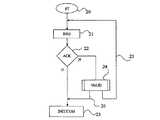
FIG. 1 schematically shows a conventional example of a data exchange system between a read / write terminal 1 and a
[0003]
In general, the terminal 1 is composed of an inductance L1 in which a capacitor C1 and a resistor R1 are connected in series between an
[0004]
Other circuits not shown are generally connected to terminal 1. Among these circuits are circuits for controlling and utilizing received data, most often based on control signals and a microprocessor for processing data. These circuits generally communicate with other input / output circuits (keyboard, screen, means for transmission to a server, etc.) and / or processing circuits not shown. The circuits of the read / write terminal draw the power necessary for their operation from a supply circuit (not shown) connected to a power supply system or battery, for example.
[0005]
The
[0006]
The terminal and transponder oscillation circuits are generally tuned to the same frequency corresponding to the frequency of the excitation signal of the terminal oscillation circuit. The high frequency signal (eg 13.56 MHz) is used not only as a transmission carrier, but also as a remote supply carrier for the transponder located in the terminal field. When the
[0007]
Next, the fluctuations in the load from the transponder are, for example, in the form of amplitude or phase changes by means of measuring the voltage across the capacitor C1, or in the form of current in the oscillation circuit by means of the demodulator 6. Can be detected.
[0008]
The invention is particularly applicable to systems with read / write terminals that use amplitude modulation to detect transponder load variations in situ and demodulate transmitted data.
[0009]
A problem with conventional electromagnetic transponder systems is that a transponder that is remotely powered by a terminal and that transmits data to the terminal may not be detected by the terminal. This means that the terminal demodulator does not detect the presence of data modulation. This phenomenon is generally called “demodulation gap”. For a particular system, this corresponds to the relative position of the terminal and transponder, at which the terminal demodulator is “blind”.
[0010]
The idea of this demodulation gap is different from what is called a “remote power supply gap”. This “remote power supply gap” does not allow the transponder to be powered by a high frequency signal, even if the transponder is in the terminal electromagnetic field. Certainly, depending on the relative position between the transponder and the terminal, the terminal does not supply power to the transponder due to the magnetic coupling between the oscillation circuits, that is, the voltage generated between the
[0011]
As a result of this demodulation gap problem, the terminal cannot detect the presence of a transponder in the field. This is because this detection conventionally uses the result of the data demodulator on the terminal side. In particular, when it is in a standby state, when waiting for transmission, the terminal periodically transmits a request for transmitting a response signal radio wave by modulating the amplitude of the remote power supply carrier wave. Subsequently, the terminal monitors the output of the demodulator, which indicates the presence of a transponder at the terminal. Certainly, when the transponder enters the terminal field, the transponder demodulates a message that causes the response signal radio wave transmitted periodically by this terminal to be transmitted to the transponder. It responds that it has been identified.
[0012]
A further disadvantage is that since the transponder received data from the terminal, the transponder believes it was recognized by the terminal, but this is not true. The only current technology to eliminate this phenomenon is to increase the exchange of information to confirm the transmission, which is expensive in terms of transmission duration.
[0013]
Other transponder systems of the type to which the present invention applies include, for example, U.S. Pat. Nos. 4,963,887 and 5,550,536, and European Patent Applications 0,722,094 and 0,857. , 981, all of which are hereby incorporated by reference.
[0014]
In a read / write terminal with an amplitude demodulator, a carrier (13.56 MHz) surrounding the self-resonant frequency of the transponder oscillator circuit L2-C2 for a specific coupling coefficient between the transponder oscillator circuits associated with the terminal. ), And the output voltage of the demodulator is invalid, that is, a demodulation gap. Ideally, the center frequency corresponds to full tuning of the remote power carrier frequency terminal and transponder, with the maximum amplitude available for demodulation.
[0015]
In order to maximize the remote supply power received by the transponder, it is anxious to tune both the terminal and the transponder oscillator circuit to the remote power supply carrier frequency. However, in particular, the manufacturing tolerance of a capacitor used in an oscillation circuit is generally about 10% as the capacitor C2 of a generally integrated transponder. As a result of this degree of manufacturing tolerances, perfect tuning is not really respected and it cannot be guaranteed that the transponder entering the terminal field is not within the demodulation gap at a particular coupling position.
[0016]
Further, the position of the demodulation gap in the amplitude demodulation response changes according to the mutual inductance between the oscillation circuits. Now, this mutual inductance depends on the distance separating the antennas L1 and L2 of the terminal and the transponder and therefore on the relative position of the transponder with respect to the transmitting terminal.
[0017]
The combined problem of the presence of demodulation gaps and the presence of changes in the position of these demodulation gaps with respect to the distance between the inductances makes conventional systems unreliable in relation to component manufacturing tolerances.
[0018]
[Problems to be solved by the invention]
It is an object of the present invention to overcome the disadvantages of prior systems related to the presence of a demodulation gap in the read / write terminal demodulator response.
[0019]
More particularly, it is an object of the present invention to provide a novel control method that makes the read / write terminal insensitive to the demodulation gap of data received from a transponder that has entered the field.
[0020]
Similarly, an object of the present invention is to provide a new terminal that is insensitive to the demodulation gap of data received from a transponder that has entered the field.
[0021]
It is also an object of the present invention to provide a solution that does not require modification of the transponder and is therefore compatible with current transponders.
[0022]
It is a further object of the present invention to provide a solution that is well suited to terminals with amplitude ditoners.
[0023]
[Means for Solving the Problems]
A terminal is provided that generates an electromagnetic field and communicates with at least one transponder (10) in the field, the terminal being excited by a high frequency remote supply signal of the transponder, and a subcarrier rate in the terminal's oscillator circuit. an amplitude demodulator for detecting data transmitted by the transponder by modulating the load in the form, and means for adjusting the signal phase of the terminal's oscillating circuit on a reference valuewith a long response time as compared to the sub-carrier Means for measuring variables linked to the current and voltage of the oscillation circuit and means for comparing the current values of these variables with predetermined values.
[0024]
According to an embodiment of the present invention, the terminal has means (39) for deactivating the phase adjusting means (37) and means for forcing the value of the setting element (31) of the oscillation circuit.
[0025]
According to an embodiment of the present invention, the setting element is a variable capacitance element of an oscillation circuit of a terminal.
[0026]
According to an embodiment of the present invention, the setting element iscontrolled by selecting one of phase adjusting means and forcing means.
[0027]
The present invention further provides a method for controlling a terminal that detects the presence of a transponder in the terminal field using the result of the comparison means.
[0028]
According to an embodiment of the present invention, the method includes the absence of a useful signal of sufficient amplitude for data detection by the demodulator (38) and the transponder (10) tothe current and voltage of the oscillator circuit of the terminal. When detected by comparingthe current value of thelinked variable with a predetermined value, the phase adjusting means is deactivated, the value of the setting element of the oscillation circuit is forced to the value C1f , and the variable is set to the predetermined value. To recover.
[0029]
According to an embodiment of the invention, the predetermined value corresponds to a value measured and stored during the terminal offload operation when no transponder is present in the field.
[0030]
According to an embodiment of the present invention, the value of the setting element is forced to a value determined by the phase adjusting means during the offload operation.
[0031]
The foregoing objects, features and advantages of the present invention will be discussed in the following non-limiting description of specific embodiments with reference to the accompanying drawings.
[0032]
DETAILED DESCRIPTION OF THE INVENTION
The same elements are denoted by the same reference numerals in different drawings. For clarity, only the terminal and transponder elements, and only the information exchange process steps necessary to understand the invention, are illustrated in the drawings and described below. In particular, details of the configuration of the modulator and demodulator are not described, but are within the ability of those skilled in the art based on the functional description described below. Furthermore, the present invention provides a transponder that uses a so-called “resistive” back-modulation to change the load that the transponder constitutes in the terminal oscillation circuit (the capacitance of the transponder oscillation circuit is fixed). However, the present invention more generally applies to any type of back modulation, eg, so-called “capacitive” back modulation.
[0033]
A feature of the present invention is to provide a direct determination of the presence of a transponder in the field of the read / write terminal, i.e. it is not necessary to interpret the demodulated data transmission signal coming from the transponder in the absence of it. is there. More particularly, the present invention provides for determining the absence of a transponder in the terminal field by other decisions independent of the presence of data transmission when there is no demodulated signal available to the terminal.
[0034]
Another feature of the present invention is to provide a corrective action that allows the terminal demodulator to correctly interpret the received data if there is a discrepancy between the demodulator result and the direct decision result. is there. This corrective action is performed by the oscillating circuit of the terminal and preferably by the capacitive element of this circuit.
[0035]
The determination of the presence or absence of a transponder in the field of the terminal is obtained according to the present invention by measuring the voltage across the terminal's oscillator circuit and the capacitive element (or a variable linked directly to this current and voltage) and This is done by comparing the obtained current value with a pre-stored value. The latter preferably corresponds to the value measured within the learning phase where the readout device is in a particular configuration.
[0036]
FIG. 2 is a simplified flow chart of a mode of execution of a sequence of confirmation of the presence of a transponder in the terminal field, applied to the read / write terminal standby state.
[0037]
As soon as the transponder read / write terminal is powered on and enters the operating state, it initiates a standby procedure after the start of configuration and phase testing (block 20, ST) during which this terminal communicates with the transponder. Wait for it to be established. The procedure includes periodically sending a sequence of requests (REQ) to possible transponders present in the terminal field (block 21). After each transmission of the request 21 for transmitting the response signal radio wave, the reading device monitors reception of an acknowledgment message (ACK) coming from the transponder that has entered the field by means of its demodulator (block 22).
[0038]
In the conventional method (not shown), when there is no confirmation of receipt, the reading device creates a loop for sending the request 21. Upon receipt of an acknowledgment (ACK), the readout device personalizes several transponders that may be present in the field, as well as a mode that checks whether the transponder is truly the transponder intended for it To a possible anti-collision mode (block 23, INIT / COM). Certainly, if there are several transponders in the terminal field, in response to the terminal requesting the response signal to be transmitted, these transponders may produce the result of demodulation by a readout device that is unavailable or not available at the same time. May react with a sufficiently small time interval. Subsequently, the readout device must either select a transponder that wishes to communicate or assign a different channel to a different transponder.
[0039]
Communication begins only when the initialization and anti-collision process illustrated in FIG. As soon as a particular transponder is properly identified, it is placed in a state where it no longer receives and confirms a request to send a response signal radio wave, in order to avoid interference with the detection of other possible transponders.
[0040]
An initialization and anti-collision process of the type briefly described above is known. Illustrations of conventional methods are found, for example, in French patent applications 2,760,280 and 2,773,627, which are hereby incorporated by reference.
[0041]
During the standby procedure or during communication, the terminal makes use of the results provided by its demodulator.
[0042]
In accordance with the present invention, the reading device expects to obtain a result from its demodulator, and whenever the result is negative (block 22), the verification procedure of the present invention (block 24, VALID) is performed. .
[0043]
When the execution of the method of the present invention confirms the absence of the transponder in the terminal field, the sending of the request for sending the response signal radio wave (link 25) is resumed. However, if the check performed by the present invention invalidates the demodulator results and indicates that the transponder must be present at the terminal field, then the terminal oscillator circuit must be modified before communication initialization. Operation is performed (link 26).
[0044]
In order to solve the problem of tolerance of the components of the transponder oscillator circuit and the drift problem, the values of these elements are also subject to change by the transponder, so according to the present invention, the phase of the terminal oscillator circuit with respect to the reference value It is provided to control. According to the invention, this phase control is performed by loop means, which is slow enough to avoid disturbing possible back modulation from the transponder and compared to the transponder's passing speed in the terminal field. And have a reaction time selected to be fast enough. This may be referred to as static control over the modulation frequency (eg, 13.56 MHz remote power supply carrier frequency and 847.5 kHz back modulation frequency used for data transmission from the transponder to the terminal).
[0045]
Such phase control of the oscillating circuit of the terminal can also be carried out by using known means, for example as described in the above-mentioned European Patent Application 0,857,981. Application of the system provided herein or other well known phase control system to practice the present invention is within the abilities of those skilled in the art based on the functional description contained in this description. is there.
[0046]
By using a phase control loop, the current and voltage measurements of the terminal oscillator circuit can be utilized in accordance with the present invention to infer information from this measurement regarding the presence of one or several transponders in the field.
[0047]
The current indicated by I in the terminal's series oscillator circuit (eg, measured by an intensity transformer) is linked to a so-called generator voltage (Vg), which excites the oscillator circuit and Linked to the apparent impedance Z1app .
[0048]
[Expression 1]
Here, considering that the series inductance and resistance of the oscillating circuit of the terminal have fixed and invariable values, the excitation voltage of the oscillating circuit is determined by a constant factor at least for a specific terminal. It is proportional to the voltage (VC1) applied to the sex element. Thus, evaluating the apparent impedance of the terminal's oscillator circuit is equivalent to evaluating the ratio between the voltage across the capacitive element and the current in the oscillator circuit.
[0050]
The assessment of the presence of the transponder performed by the present invention is based on the information on the current in the terminal's oscillator circuit and the voltage on it, and more particularly on its capacitive element (or its constant and determined factor). Information linked directly to the variable) is used exclusively.
[0051]
According to the invention, so-called “offload” values of current and voltage are used when no transponder is present in the terminal field. These electrical magnitudes can be easily measured on the read / write terminal side, for example in the learning phase, for example following installation at the terminal usage location.
[0052]
Thereafter, the presence of a transponder in the field can be inferred by evaluating the current ratio (or link information) between the voltage across the capacitive element and the current in the oscillator circuit.
[0053]
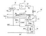
FIG. 3 schematically shows a first embodiment of a read / write terminal according to the present invention comprising a phase control loop of an oscillation circuit and an amplitude demodulator.
[0054]
Traditionally, terminal 30 was in series with
[0055]
The phase control of the current in the antenna L1 is performed with respect to the reference signal. This control is control of the high frequency signal, that is, control of the carrier wave signal corresponding to the signal E in a state where there is no data to be transmitted. This control is performed by changing the capacity of the oscillation circuit of the terminal 30 in order to maintain the current in the antenna in a fixed relationship with the reference signal corresponding to the signal OSC supplied by the oscillator of the modulator, for example. . However, this control is slow enough to only consider the static phase change with respect to the back modulated carrier. The signal CTRL is generated from a circuit (COMP) 37 having a function of detecting the phase interval with respect to the reference signal and correcting the capacitance of the
[0056]
In accordance with the present invention, signal MES1 is also sent to a microprocessor or equivalent, as previously indicated, to perform the verification method of the present invention. The second measurement signal MES2 provides information related to the voltage VC1 across the
[0057]
The terminal 30 receives, for example, a voltage VC1 (or a current image) applied to the capacitive element 31 (more specifically, a series combination of the
[0058]
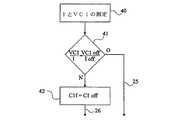
FIG. 4 is a flowchart of an embodiment of the confirmation method (block 24, FIG. 2) of the present invention.
[0059]
As previously indicated, current I and voltage VC1 are first measured in the oscillator circuit (block 40). Subsequently, the ratio of voltage VC1 to current I is compared to the same value measured offload (VC1off-load and Ioff-load ) at the learning phase (block 41). If the two ratios are the same, this means that there is no transponder in the terminal field and the confirmation process provides this information (link 25). However, if the two ratios are different, this means that the demodulator is in the demodulation gap, even if the transponder is in the terminal field.
[0060]
The imaginary part X1app of the apparent impedance Z1app of the oscillation circuit of the terminal can be expressed as follows.
[0061]
X1app = X1-a2 . X2 (2)
[0062]
Here, X1 represents the imaginary part of the impedance of the oscillation circuit of the terminal.
Ie:
[0063]
[Expression 2]
Here, X2 represents the imaginary part of the oscillation circuit of the transponder.
[0065]
[Equation 3]
further:
[0067]
[Expression 4]
Here, ω represents a pulse, R2 represents a load applied to the oscillation circuit of the transponder on its own oscillation circuit, and is modeled by a resistor parallel to the inductance L2 and the capacitor C2. In other words, resistor R2 represents the equivalent resistance of the entire transponder circuit added in parallel with capacitor C2 and inductance L2 (microprocessor, back modulation means, etc.).
[0069]
Due to the phase control, the imaginary part X1app is zero. Therefore:
[0070]
Based on these relationships, the difference between thecurrent value and the off-road value is expressed as follows:
[0071]
X1-X1off-load = a2 . X2-aoff-load2 . X2 (7)
[0072]
At this time, since the off-road coupling is zero, the coefficient aoff-load is also zero. Furthermore, the voltage VC1 applied to the element 31 (ignoring the influence of the intensity transformer 35) can be written as I / ωC1. As a result, the above equation (7) can be written as follows.
[0073]
[Equation 5]
If equation (8) above is not zero, this is not only that the transponder is in the terminal field, but for this transponder, the variable X2 is not zero, that is, the tuning of the oscillator circuit is It means that it is off even if it is slight. This is in full agreement with the fact that the transponder radiates data to the terminal, ie it modifies the load that the transponder creates on the terminal's oscillator circuit.
[0075]
In other words, it can be considered that the above formula is invalid only in the case of two. The first case corresponds to the case where no transponder is present at the terminal. The second case is when the capacitor C2 of the transponder oscillator circuit is fully tuned to the remote power supply carrier. In this case, X2 = 0.
[0076]
In practice, the transponder technical variation and the operational drift result in a variation of around 10% of the capacitance of the capacitor C2 with respect to the tuning value C2tun . In addition, to correct these variations, there is generally nothing you can do with the transponder. This is particularly the reason why the phase control loop allows optimizing the transponder's remote power supply by correcting these possible drifts by modifying the read / write terminal side tuning.
[0077]
In order to get out of the demodulation gap, the correction performed in accordance with the present invention involves forcibly changing the value of the capacitance C1 of the
[0078]
Force value of capacitor C1,the
[0079]
Note that the phase of oscillation is not controlled by forcing the capacitance value to change. However, this correction according to the invention only interferes in the very special case where the demodulator is “blind”. Of course, the control value of the capacity is recovered as soon as this situation disappears, for example, as soon as the communication with the relevant transponder ends.
[0080]
According to the modification according to the invention, the capacitance C1 of the
[0081]
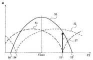
FIG. 5 shows an embodiment of the method according to the invention by showing three examples of the deviation amplitude dI of the current I that can be used for amplitude demodulation according to the transponder capacitance C2 present in the terminal field. In other words, this indicates a signal that can be used to take advantage of the back modulation coming from the transponder by means of amplitude demodulation.
[0082]
The deviation dI corresponds to the voltage deviation dV applied to the
[0083]
The
[0084]
For this ideal case, two types of curves can be defined, the long and short dotted line 51 and the dotted
[0085]
Performing the correction provided by the present invention corresponds to moving the operating point of the readout device to reach the ideal curve (shape 50). This action is represented by the
[0086]
According to a particular embodiment in which the
[0087]
[Formula 6]
An advantage of the present invention is that the reliability of the operation of the read / write terminal of the electromagnetic transponder is improved by the determination of electrical variables that can be easily measured.
[0089]
Another advantage of the present invention is that it can only be performed on the read / write terminal side. Thus, the operation of the transponders present in the terminal field is not modified and the present invention can be implemented for current conventional transponders.
[0090]
Another advantage of the present invention is that the structural modification of the terminal is minimized by selecting the setting of the static phase control loop variables.
[0091]
Another advantage of the present invention is that it makes the operation of the transponder system insensitive to the demodulation gap.
[0092]
Another advantage of the present invention is that the corrections made do not adversely affect the transponder remote power supply.
[0093]
Another advantage of the present invention is that it does not require adaptation due to the sensitivity of the demodulator. It can even be considered that the present invention automatically adapts to the demodulator gap deviation. Certainly, this is independent of the detection threshold of the demodulator because the correction performed by the present invention is performed based on the result of the demodulation.
[0094]
Of course, the present invention is likely to have various alterations, modifications and improvements that will readily occur to those skilled in the art. In particular, by means of conventional components of a read / write terminal, the practical implementation of the verification process of the present invention is within the capabilities of those skilled in the art, based on the description of the functions described above and the applications studied. Is.
[0095]
Further, although the above description has been given of the case where there is a transponder with which the terminal communicates, the present invention also applies to the case where several transponders must communicate with the same terminal. Simply put, as soon as one of the transponders is identified as presenting a problem with the demodulation gap, it can be provided to forcibly change the value of the capacitance C1. Thus, useful signal attenuation that may be introduced to other transponders is considered to be tolerable. However, in the preferred embodiment, the fact that the value overridden for the transponder has a slight risk of placing other transponders in the demodulation gap is taken into account. It is provided to individualize the capacity values of the
[0096]
Further, in the above description, it has been considered that the value of the capacitor C2 is fixed, that is, the back modulation is performed by changing the equivalent resistance R2. However, the present invention replaces the case of “capacitive” back modulation that modifies the value of the capacitance C2 at the speed of the secondary carrier. In this case, the demodulation gap depends on the resistance R2, and thus varies with the consumption of the transponder circuit. The detection principle discussed above is not modified. The correction is simply adapted to the terminal side.
[0097]
Finally, even if a determination based on the voltage across the
[0098]
Such alterations, modifications, and improvements are also intended to be part of this disclosure, and are intended to be within the spirit and scope of the invention. Accordingly, the above description is merely an example and is not intended to be limiting. The invention is limited only as defined in the following claims and the equivalents herein.
[Brief description of the drawings]
FIG. 1 is a schematic diagram of a conventional example of an electromagnetic transponder system.
FIG. 2 shows, in simplified flowchart form, one embodiment of a method for confirming the presence of a transponder according to the present invention.
FIG. 3 is a diagrammatic representation, in part, of one embodiment of an amplitude demodulated read / write terminal according to the present invention.
FIG. 4 is a diagram showing, in the form of a flowchart, the mode of execution of the checking method according to the invention for phase demodulation.
FIG. 5 shows an example of the amplitude shape of the demodulated signal available at the input of the amplitude demodulator of this terminal according to the capacity of the transponder oscillator circuit in the field of the read / write terminal.
[Explanation of symbols]
1, 4, 7
Claims (8)
Translated fromJapaneseトランスポンダの高周波遠隔供給信号により励起される発振回路と、
ターミナルの発振回路にサブキャリアのレートで形成される負荷を変調することによりトランスポンダにより送信されるデータを検出する振幅復調器(38)と、
ターミナルの発振回路の信号位相を前記サブキャリアに比較して長い応答時間で基準値に調節する位相調節手段と、
発振回路の電流と電圧にリンクした変数を測定する手段と、
これら変数の現在値を所定の値(Ioff−load、VC1off−load)と比較する比較手段とを有することを特徴とするターミナル。In a terminal (30) that generates an electromagnetic field and communicates with at least one transponder (10) in the field,
An oscillation circuit excited by a high frequency remote supply signal of the transponder;
An amplitude demodulator (38) for detecting data transmitted by the transponder by modulating the load formed at the subcarrier rate in the oscillation circuit of the terminal;
Aphase adjusting means for adjusting the reference valuein a long response time signal phase of the terminal's oscillating circuit as compared to the sub-carrier,
Means for measuring variables linked to the current and voltage of the oscillator circuit;
A terminal havingcomparison means forcomparing current values of these variables with predetermined values (Ioff-load , VC1off-load ).
位相調節手段(37)を非活性化し、
発振回路(R1,L1,31)の設定素子(31)の値を強制変更値C1fに強制して、前記変数(I,VC1)が前記所定の値(Ioff−load、VC1off−load)を回復するようにする、請求項5記載の方法。The absence of a useful signal of sufficient amplitude for data detection by theamplitude demodulator (38) and the transponder (10)between the current value and the predetermined value ofthe variable linked to the current and voltage of the oscillation circuit of the terminal When detected by comparison,
Deactivating the phase adjusting means (37);
The value of the setting element (31) of the oscillation circuit (R1, L1, 31) isforced to theforced change value C1f , and the variables (I, VC1) are set to the predetermined values (Ioff-load , VC1off-load). 6. The method of claim 5, wherein the method is recovered.
Applications Claiming Priority (2)
| Application Number | Priority Date | Filing Date | Title |
|---|---|---|---|
| FR0006061 | 2000-05-12 | ||
| FR0006061AFR2808941B1 (en) | 2000-05-12 | 2000-05-12 | VALIDATION OF THE PRESENCE OF AN ELECTROMAGNETIC TRANSPONDER IN THE FIELD OF AN AMPLITUDE DEMODULATION READER |
Publications (3)
| Publication Number | Publication Date |
|---|---|
| JP2002009659A JP2002009659A (en) | 2002-01-11 |
| JP2002009659A5 JP2002009659A5 (en) | 2011-03-24 |
| JP4715027B2true JP4715027B2 (en) | 2011-07-06 |
Family
ID=8850147
Family Applications (1)
| Application Number | Title | Priority Date | Filing Date |
|---|---|---|---|
| JP2001141587AExpired - Fee RelatedJP4715027B2 (en) | 2000-05-12 | 2001-05-11 | Confirmation of the presence of an electromagnetic transponder in the field of an amplitude demodulation reader. |
Country Status (5)
| Country | Link |
|---|---|
| US (1) | US7005967B2 (en) |
| EP (1) | EP1164534B1 (en) |
| JP (1) | JP4715027B2 (en) |
| DE (1) | DE60101867T2 (en) |
| FR (1) | FR2808941B1 (en) |
Families Citing this family (18)
| Publication number | Priority date | Publication date | Assignee | Title |
|---|---|---|---|---|
| TW417249B (en)* | 1997-05-14 | 2001-01-01 | Applied Materials Inc | Reliability barrier integration for cu application |
| US7049935B1 (en) | 1999-07-20 | 2006-05-23 | Stmicroelectronics S.A. | Sizing of an electromagnetic transponder system for a dedicated distant coupling operation |
| FR2796781A1 (en) | 1999-07-20 | 2001-01-26 | St Microelectronics Sa | DIMENSIONING OF AN ELECTROMAGNETIC TRANSPONDER SYSTEM FOR HYPERPROXIMITY OPERATION |
| FR2804557B1 (en)* | 2000-01-31 | 2003-06-27 | St Microelectronics Sa | ADAPTING THE TRANSMISSION POWER OF AN ELECTROMAGNETIC TRANSPONDER DRIVE |
| FR2808946A1 (en)* | 2000-05-12 | 2001-11-16 | St Microelectronics Sa | VALIDATION OF THE PRESENCE OF AN ELECTROMAGNETIC TRANSPONDER IN THE FIELD OF A READER |
| FR2808942B1 (en)* | 2000-05-12 | 2002-08-16 | St Microelectronics Sa | VALIDATION OF THE PRESENCE OF AN ELECTROMAGNETIC TRANSPONDER IN THE FIELD OF A PHASE DEMODULATION READER |
| FR2808945B1 (en)* | 2000-05-12 | 2002-08-16 | St Microelectronics Sa | EVALUATION OF THE NUMBER OF ELECTROMAGNETIC TRANSPONDERS IN THE FIELD OF A READER |
| FR2809251B1 (en)* | 2000-05-17 | 2003-08-15 | St Microelectronics Sa | DEVICE FOR PRODUCING AN ELECTROMAGNETIC FIELD FOR A TRANSPONDER |
| FR2809235A1 (en)* | 2000-05-17 | 2001-11-23 | St Microelectronics Sa | ANTENNA FOR GENERATING AN ELECTROMAGNETIC FIELD FOR TRANSPONDER |
| FR2812986B1 (en)* | 2000-08-09 | 2002-10-31 | St Microelectronics Sa | DETECTION OF AN ELECTRIC SIGNATURE OF AN ELECTROMAGNETIC TRANSPONDER |
| US20030169169A1 (en)* | 2000-08-17 | 2003-09-11 | Luc Wuidart | Antenna generating an electromagnetic field for transponder |
| FR2854288B1 (en)* | 2003-04-23 | 2005-05-27 | Commissariat Energie Atomique | RF TRANSMITTING-RECEIVING DEVICE |
| FR2947075A1 (en) | 2009-06-19 | 2010-12-24 | St Microelectronics Rousset | RESISTIVE EVALUATION OF THE COUPLING FACTOR OF AN ELECTROMAGNETIC TRANSPONDER |
| US8362902B2 (en)* | 2009-07-24 | 2013-01-29 | Electronics And Telecommunications Research Institute | RFID reader and method for identifying RFID tag thereof and apparatus for analyzing reception power pattern |
| FR2976102B1 (en) | 2011-06-03 | 2013-05-17 | St Microelectronics Rousset | ASSISTING THE POSITIONING OF A TRANSPONDER |
| FR2976103B1 (en) | 2011-06-03 | 2013-05-17 | St Microelectronics Rousset | ASSISTING THE POSITIONING OF A TRANSPONDER |
| FR2976104B1 (en) | 2011-06-03 | 2013-11-15 | St Microelectronics Rousset | SECURING COMMUNICATION BETWEEN AN ELECTROMAGNETIC TRANSPONDER AND A TERMINAL |
| FR2976105B1 (en) | 2011-06-03 | 2013-05-17 | St Microelectronics Rousset | SECURING COMMUNICATION BY AN ELECTROMAGNETIC TRANSPONDER |
Family Cites Families (112)
| Publication number | Priority date | Publication date | Assignee | Title |
|---|---|---|---|---|
| GB579414A (en) | 1941-10-15 | 1946-08-02 | Standard Telephones Cables Ltd | Improvements in or relating to electric wave filters |
| US5202644A (en) | 1959-06-11 | 1993-04-13 | Ail Systems, Inc. | Receiver apparatus |
| US3618089A (en) | 1969-01-29 | 1971-11-02 | Moran Instr Corp | Range and time measure system |
| GB1341025A (en) | 1970-11-17 | 1973-12-19 | English Electric Co Ltd | Data transmission over mains supplies |
| US4068232A (en) | 1976-02-12 | 1978-01-10 | Fairchild Industries, Inc. | Passive encoding microwave transponder |
| JPS53120295A (en) | 1977-03-30 | 1978-10-20 | Toshiba Corp | Subject discrimination device |
| DE2732543C3 (en) | 1977-07-19 | 1980-08-07 | Precitec Gesellschaft Fuer Praezisionstechnik Und Elektronik Mbh & Co Entwicklungs- Und Vertriebs-Kg, 7570 Baden-Baden | Device for detecting objects located in the area of an interface |
| DK362277A (en) | 1977-08-15 | 1979-02-16 | Medibit A S | ELECTRONIC INFORMATION SYSTEM |
| DK146108C (en) | 1978-11-13 | 1983-11-21 | Medibit A S | PROCEDURE FOR TRANSFER INFORMATION AND APPLICATIONS FOR EXERCISING THE PROCEDURE |
| US4278977A (en) | 1979-05-04 | 1981-07-14 | Rca Corporation | Range determining system |
| US4258348A (en)* | 1979-11-13 | 1981-03-24 | Stb Transformer Company | Current measuring transformer |
| ATE14055T1 (en) | 1980-04-28 | 1985-07-15 | Paul Rouet | METHOD AND SYSTEM FOR THE TRANSMISSION OF MESSAGES AND CONTROL ON AN AC SUPPLY NETWORK. |
| US4928108A (en) | 1983-12-20 | 1990-05-22 | Bsh Electronics, Ltd. | Electrical signal separating device having isolating and matching circuitry for split passband matching |
| US4673932A (en) | 1983-12-29 | 1987-06-16 | Revlon, Inc. | Rapid inventory data acquistion system |
| US4593412A (en) | 1984-05-21 | 1986-06-03 | Multi-Elmac Company | Integrated oscillator antenna for low power, low harmonic radiation |
| US4706050A (en) | 1984-09-22 | 1987-11-10 | Smiths Industries Public Limited Company | Microstrip devices |
| US4656472A (en) | 1985-01-23 | 1987-04-07 | Walton Charles A | Proximity identification system with power aided identifier |
| JPS61196603A (en) | 1985-02-26 | 1986-08-30 | Mitsubishi Electric Corp | Antenna |
| US4660192A (en) | 1985-04-11 | 1987-04-21 | Pomatto Sr Robert P | Simultaneous AM and FM transmitter and receiver |
| US4782308A (en) | 1986-03-07 | 1988-11-01 | Iskra-Sozd Elektrokovinske Industrije N.Sol.O | Circuit arrangement of a reading device for electromagnetic identification cards |
| GB2197107B (en) | 1986-11-03 | 1990-12-12 | Mars Inc | Data-storing devices |
| IL82025A (en) | 1987-03-27 | 1993-07-08 | Galil Electro Ltd | Electronic data communications system |
| US4802080A (en) | 1988-03-18 | 1989-01-31 | American Telephone And Telegraph Company, At&T Information Systems | Power transfer circuit including a sympathetic resonator |
| US5701121A (en) | 1988-04-11 | 1997-12-23 | Uniscan Ltd. | Transducer and interrogator device |
| JP2612190B2 (en) | 1988-08-31 | 1997-05-21 | 山武ハネウエル株式会社 | Full-duplex communication device consisting of answering device and interrogation device |
| US5055853A (en) | 1988-10-03 | 1991-10-08 | Garnier Robert C | Magnetic frill generator |
| EP0369622A3 (en) | 1988-11-09 | 1991-04-17 | Security Tag Systems, Inc. | Proximity reading of coded tag |
| US5305008A (en) | 1991-08-12 | 1994-04-19 | Integrated Silicon Design Pty. Ltd. | Transponder system |
| US5084699A (en) | 1989-05-26 | 1992-01-28 | Trovan Limited | Impedance matching coil assembly for an inductively coupled transponder |
| US5099227A (en) | 1989-07-18 | 1992-03-24 | Indala Corporation | Proximity detecting apparatus |
| US5126749A (en) | 1989-08-25 | 1992-06-30 | Kaltner George W | Individually fed multiloop antennas for electronic security systems |
| US5142292A (en) | 1991-08-05 | 1992-08-25 | Checkpoint Systems, Inc. | Coplanar multiple loop antenna for electronic article surveillance systems |
| US5235326A (en) | 1991-08-15 | 1993-08-10 | Avid Corporation | Multi-mode identification system |
| US5214409A (en) | 1991-12-03 | 1993-05-25 | Avid Corporation | Multi-memory electronic identification tag |
| ATE148812T1 (en) | 1992-02-29 | 1997-02-15 | Scantronic Ltd | POWER SUPPLY, ESPECIALLY FOR ALARM SYSTEM |
| SE469959B (en) | 1992-03-06 | 1993-10-11 | Electrolux Ab | Device for transmitting control commands in an AC or machine |
| US5452344A (en) | 1992-05-29 | 1995-09-19 | Datran Systems Corporation | Communication over power lines |
| NL9201270A (en) | 1992-07-15 | 1994-02-01 | Nedap Nv | ANTI-SHOP THEFT ANTENNA WITH ROTATING FIELD. |
| JP2747395B2 (en) | 1992-07-20 | 1998-05-06 | 三菱電機株式会社 | Non-contact IC card, non-contact IC card reader / writer, and data transmission method |
| NZ314270A (en) | 1992-11-18 | 1998-06-26 | British Tech Group | Transponder identification system: interrogator transmits inhibiting signal to disable transponders |
| DE4327642C2 (en) | 1993-05-17 | 1998-09-24 | Anatoli Stobbe | Reader for a detection plate |
| US5451958A (en) | 1993-05-21 | 1995-09-19 | Texas Instruments Deutschland Gmbh | Dual standard RF-ID system |
| US5850416A (en) | 1993-06-30 | 1998-12-15 | Lucent Technologies, Inc. | Wireless transmitter-receiver information device |
| US5324315A (en) | 1993-08-12 | 1994-06-28 | Medtronic, Inc. | Closed-loop downlink telemetry and method for implantable medical device |
| US5541604A (en) | 1993-09-03 | 1996-07-30 | Texas Instruments Deutschland Gmbh | Transponders, Interrogators, systems and methods for elimination of interrogator synchronization requirement |
| JPH085731A (en) | 1993-10-04 | 1996-01-12 | Texas Instr Deutschland Gmbh | Determination of position of rf -id transponder |
| US5521602A (en) | 1994-02-10 | 1996-05-28 | Racom Systems, Inc. | Communications system utilizing FSK/PSK modulation techniques |
| US5504485A (en) | 1994-07-21 | 1996-04-02 | Amtech Corporation | System for preventing reading of undesired RF signals |
| US5550536A (en) | 1994-08-17 | 1996-08-27 | Texas Instruments Deutschland Gmbh | Circuit frequency following technique transponder resonant |
| FR2724477B1 (en) | 1994-09-13 | 1997-01-10 | Gemplus Card Int | NON-CONTACT CARD MANUFACTURING PROCESS |
| JPH0962816A (en) | 1994-10-06 | 1997-03-07 | Mitsubishi Electric Corp | Contactless IC card and contactless IC card system including the same |
| JPH08123919A (en) | 1994-10-28 | 1996-05-17 | Mitsubishi Electric Corp | Non-contact IC card system and communication method thereof |
| JPH08191259A (en) | 1995-01-11 | 1996-07-23 | Sony Chem Corp | Transmitter-receiver for contactless ic card system |
| GB9503352D0 (en) | 1995-02-21 | 1995-04-12 | Sinnett Glyn | Remote control system |
| US5691605A (en) | 1995-03-31 | 1997-11-25 | Philips Electronics North America | Electronic ballast with interface circuitry for multiple dimming inputs |
| US5604411A (en) | 1995-03-31 | 1997-02-18 | Philips Electronics North America Corporation | Electronic ballast having a triac dimming filter with preconditioner offset control |
| JPH095430A (en) | 1995-06-22 | 1997-01-10 | Fujitsu Ten Ltd | Antenna driving device for transponder |
| SE513690C2 (en) | 1995-08-16 | 2000-10-23 | Alfa Laval Agri Ab | Antenna system with transponder drive circuits |
| US6243013B1 (en) | 1999-01-08 | 2001-06-05 | Intermec Ip Corp. | Cascaded DC voltages of multiple antenna RF tag front-end circuits |
| JPH0981701A (en) | 1995-09-19 | 1997-03-28 | Toshiba Corp | Contactless information recording medium and contactless information transmission method |
| JPH09218263A (en) | 1995-10-11 | 1997-08-19 | Texas Instr Inc <Ti> | Transponder system and operating method thereof |
| DE19541855C1 (en) | 1995-11-09 | 1997-02-20 | Siemens Ag | Theft protection system for motor vehicles |
| NL1001761C2 (en) | 1995-11-28 | 1997-05-30 | Ronald Barend Van Santbrink | System for contactless data exchange between a reading and writing unit and one or more information carriers. |
| DE19546928A1 (en) | 1995-12-15 | 1997-06-19 | Diehl Ident Gmbh | Inductive high frequency information signal transmitter |
| SE506449C2 (en) | 1996-02-12 | 1997-12-15 | Rso Corp | Article Surveillance systems |
| FR2746200B1 (en) | 1996-03-12 | 1998-05-29 | NON-CONTACT INFORMATION EXCHANGE DEVICE WITH AN ELECTRONIC LABEL | |
| DE19621076C2 (en) | 1996-05-24 | 2001-06-28 | Siemens Ag | Device and method for the contactless transmission of energy or data |
| AUPO055296A0 (en) | 1996-06-19 | 1996-07-11 | Integrated Silicon Design Pty Ltd | Enhanced range transponder system |
| DE19632282A1 (en) | 1996-08-09 | 1998-02-19 | Holzer Walter Prof Dr H C Ing | Process and device for controlling the brightness of fluorescent lamps |
| AU4458297A (en) | 1996-09-13 | 1998-04-02 | Temic Telefunken Microelectronik Gmbh | Method for tuning an oscillating receiver circuit of a transponder built into a rfid system |
| JPH10145267A (en) | 1996-09-13 | 1998-05-29 | Hitachi Ltd | High efficiency antenna coil, wireless card and information communication system using wireless card |
| US6446049B1 (en) | 1996-10-25 | 2002-09-03 | Pole/Zero Corporation | Method and apparatus for transmitting a digital information signal and vending system incorporating same |
| EP0871897A1 (en)* | 1996-11-05 | 1998-10-21 | Koninklijke Philips Electronics N.V. | Contactless data transmission and receiving device with a synchronous demodulator |
| FR2757952B1 (en) | 1996-12-27 | 1999-03-19 | Gemplus Card Int | RADIO TRANSPONDER PROVIDED WITH AN ANTENNA AND A FREQUENCY TUNING CIRCUIT |
| US6304169B1 (en) | 1997-01-02 | 2001-10-16 | C. W. Over Solutions, Inc. | Inductor-capacitor resonant circuits and improved methods of using same |
| JPH10203066A (en) | 1997-01-28 | 1998-08-04 | Hitachi Ltd | Non-contact IC card |
| EP0857981B1 (en)* | 1997-02-05 | 2002-12-11 | EM Microelectronic-Marin SA | Base station of a remote interrogation system with a voltage and phase controlled oscillator |
| TW376598B (en) | 1997-02-05 | 1999-12-11 | Em Microelectronic Marin Sa | Base station for a contactless interrogation system comprising a phase locked and voltage controlled oscillator |
| US5883582A (en) | 1997-02-07 | 1999-03-16 | Checkpoint Systems, Inc. | Anticollision protocol for reading multiple RFID tags |
| FR2760280B1 (en) | 1997-03-03 | 1999-05-21 | Innovatron Ind Sa | METHOD FOR MANAGING COLLISIONS IN A CONTACTLESS DATA EXCHANGE SYSTEM |
| US6208235B1 (en) | 1997-03-24 | 2001-03-27 | Checkpoint Systems, Inc. | Apparatus for magnetically decoupling an RFID tag |
| JP3916291B2 (en) | 1997-03-28 | 2007-05-16 | ローム株式会社 | Information communication equipment |
| JP3427668B2 (en) | 1997-04-01 | 2003-07-22 | 株式会社村田製作所 | Antenna device |
| JP3792002B2 (en)* | 1997-04-17 | 2006-06-28 | ローム株式会社 | Data communication apparatus, data communication system, and data communication method |
| JPH1131913A (en) | 1997-05-15 | 1999-02-02 | Murata Mfg Co Ltd | Chip antenna and mobile communication device using the antenna |
| US6025780A (en) | 1997-07-25 | 2000-02-15 | Checkpoint Systems, Inc. | RFID tags which are virtually activated and/or deactivated and apparatus and methods of using same in an electronic security system |
| JPH1166248A (en) | 1997-08-12 | 1999-03-09 | Mitsubishi Electric Corp | Non-contact IC card |
| US5986570A (en) | 1997-09-03 | 1999-11-16 | Micron Communications, Inc. | Method for resolving signal collisions between multiple RFID transponders in a field |
| US6393045B1 (en) | 1997-09-26 | 2002-05-21 | Wherenet Corp. | Spread spectrum baseband modulation of magnetic fields for communications and proximity sensing |
| GB9727042D0 (en) | 1997-12-22 | 1998-02-18 | Advanced Technology Communicat | Tag and detection system |
| US6100788A (en) | 1997-12-29 | 2000-08-08 | Storage Technology Corporation | Multifunctional electromagnetic transponder device and method for performing same |
| US6281794B1 (en) | 1998-01-02 | 2001-08-28 | Intermec Ip Corp. | Radio frequency transponder with improved read distance |
| KR20010006519A (en) | 1998-02-19 | 2001-01-26 | 비센트 비.인그라시아 | Data communications terminal and method of adjusting a power signal generated therefrom |
| TW386617U (en) | 1998-02-23 | 2000-04-01 | Kye Systems Corp | High frequency wireless pointer apparatus |
| FR2781587B1 (en) | 1998-07-21 | 2000-09-08 | Dassault Electronique | ADVANCED READER FOR NON-CONTACT BADGES |
| US5955950A (en) | 1998-07-24 | 1999-09-21 | Checkpoint Systems, Inc. | Low noise signal generator for use with an RFID system |
| US6072383A (en) | 1998-11-04 | 2000-06-06 | Checkpoint Systems, Inc. | RFID tag having parallel resonant circuit for magnetically decoupling tag from its environment |
| US6356738B1 (en) | 1999-02-18 | 2002-03-12 | Gary W. Schneider | Method and apparatus for communicating data with a transponder |
| US6424820B1 (en) | 1999-04-02 | 2002-07-23 | Interval Research Corporation | Inductively coupled wireless system and method |
| FR2792132B1 (en) | 1999-04-07 | 2001-11-02 | St Microelectronics Sa | READING TERMINAL OF AN ELECTROMAGNETIC TRANSPONDER OPERATING IN VERY CLOSE COUPLING |
| FR2792135B1 (en) | 1999-04-07 | 2001-11-02 | St Microelectronics Sa | VERY CLOSE COMPLAGE OPERATION OF AN ELECTROMAGNETIC TRANSPONDER SYSTEM |
| US6650226B1 (en) | 1999-04-07 | 2003-11-18 | Stmicroelectronics S.A. | Detection, by an electromagnetic transponder reader, of the distance separating it from a transponder |
| JP3582403B2 (en)* | 1999-05-21 | 2004-10-27 | 株式会社デンソー | Reader / writer for ID tag |
| JP3635990B2 (en)* | 1999-07-19 | 2005-04-06 | 株式会社デンソー | Reader / writer for ID tag |
| US6307468B1 (en) | 1999-07-20 | 2001-10-23 | Avid Identification Systems, Inc. | Impedance matching network and multidimensional electromagnetic field coil for a transponder interrogator |
| US6335665B1 (en)* | 1999-09-28 | 2002-01-01 | Lucent Technologies Inc. | Adjustable phase and delay shift element |
| US6650227B1 (en) | 1999-12-08 | 2003-11-18 | Hid Corporation | Reader for a radio frequency identification system having automatic tuning capability |
| US6617962B1 (en) | 2000-01-06 | 2003-09-09 | Samsys Technologies Inc. | System for multi-standard RFID tags |
| US6307517B1 (en) | 2000-06-13 | 2001-10-23 | Applied Wireless Identifications Group, Inc. | Metal compensated radio frequency identification reader |
| US6229443B1 (en) | 2000-06-23 | 2001-05-08 | Single Chip Systems | Apparatus and method for detuning of RFID tag to regulate voltage |
| DE10163633A1 (en) | 2001-12-21 | 2003-07-10 | Philips Intellectual Property | Current source circuit |
| FR2840742A1 (en) | 2002-06-06 | 2003-12-12 | St Microelectronics Sa | ELECTROMAGNETIC TRANSPONDER READER |
- 2000
- 2000-05-12FRFR0006061Apatent/FR2808941B1/ennot_activeExpired - Fee Related
- 2001
- 2001-05-11DEDE60101867Tpatent/DE60101867T2/ennot_activeExpired - Lifetime
- 2001-05-11JPJP2001141587Apatent/JP4715027B2/ennot_activeExpired - Fee Related
- 2001-05-11EPEP01410051Apatent/EP1164534B1/ennot_activeExpired - Lifetime
- 2001-05-11USUS09/854,144patent/US7005967B2/ennot_activeExpired - Lifetime
Also Published As
| Publication number | Publication date |
|---|---|
| DE60101867T2 (en) | 2004-10-28 |
| DE60101867D1 (en) | 2004-03-04 |
| FR2808941A1 (en) | 2001-11-16 |
| US20020008611A1 (en) | 2002-01-24 |
| EP1164534B1 (en) | 2004-01-28 |
| JP2002009659A (en) | 2002-01-11 |
| EP1164534A1 (en) | 2001-12-19 |
| US7005967B2 (en) | 2006-02-28 |
| FR2808941B1 (en) | 2002-08-16 |
Similar Documents
| Publication | Publication Date | Title |
|---|---|---|
| JP4715025B2 (en) | Confirmation of the presence of electromagnetic transponders in the field of the reader | |
| JP4715026B2 (en) | Confirmation of the presence of an electromagnetic transponder in the field of a phase demodulation reader. | |
| JP4715027B2 (en) | Confirmation of the presence of an electromagnetic transponder in the field of an amplitude demodulation reader. | |
| US8988196B2 (en) | Power recovery by an electromagnetic transponder | |
| US6473028B1 (en) | Detection of the distance between an electromagnetic transponder and a terminal | |
| JP5668196B2 (en) | Inductivity evaluation of coupling coefficient of electromagnetic transponder | |
| US20110140852A1 (en) | Power management in an electromagnetic transponder | |
| US8798533B2 (en) | Evaluation of the coupling factor of an electromagnetic transponder by capacitive detuning | |
| JP5501871B2 (en) | Terminal authentication by electromagnetic transponder | |
| JP5607995B2 (en) | Authentication by terminal and transponder combination by transponder | |
| JP5519425B2 (en) | Authentication by the terminal of the terminal and transponder combination | |
| US7046121B2 (en) | Detection of an electric signature of an electromagnetic transponder | |
| US9098788B2 (en) | Optimization of the processing speed of an electromagnetic transponder | |
| JP4691825B2 (en) | Evaluation of the number of electromagnetic transponders in the reader field | |
| US9407307B2 (en) | Transponder positioning aid | |
| JP2011078040A (en) | Mobile communication device, reader/writer device, and resonance frequency regulation method | |
| JP2005063123A (en) | Non-contact type IC card reader / writer device, automatic adjustment method of antenna natural frequency, program | |
| US9344156B2 (en) | Protection of communication by an electromagnetic transponder | |
| JPH10302032A (en) | Reader/writer for non-contact ic card | |
| JPH10135866A (en) | Contactless ic card system |
Legal Events
| Date | Code | Title | Description |
|---|---|---|---|
| A621 | Written request for application examination | Free format text:JAPANESE INTERMEDIATE CODE: A621 Effective date:20080327 | |
| A977 | Report on retrieval | Free format text:JAPANESE INTERMEDIATE CODE: A971007 Effective date:20101112 | |
| A131 | Notification of reasons for refusal | Free format text:JAPANESE INTERMEDIATE CODE: A131 Effective date:20101116 | |
| A524 | Written submission of copy of amendment under article 19 pct | Free format text:JAPANESE INTERMEDIATE CODE: A524 Effective date:20110203 | |
| A01 | Written decision to grant a patent or to grant a registration (utility model) | Free format text:JAPANESE INTERMEDIATE CODE: A01 Effective date:20110301 | |
| A61 | First payment of annual fees (during grant procedure) | Free format text:JAPANESE INTERMEDIATE CODE: A61 Effective date:20110314 | |
| R150 | Certificate of patent or registration of utility model | Free format text:JAPANESE INTERMEDIATE CODE: R150 | |
| FPAY | Renewal fee payment (event date is renewal date of database) | Free format text:PAYMENT UNTIL: 20140408 Year of fee payment:3 | |
| LAPS | Cancellation because of no payment of annual fees |