JP4714953B2 - Flat panel display - Google Patents
Flat panel displayDownload PDFInfo
- Publication number
- JP4714953B2 JP4714953B2JP00677699AJP677699AJP4714953B2JP 4714953 B2JP4714953 B2JP 4714953B2JP 00677699 AJP00677699 AJP 00677699AJP 677699 AJP677699 AJP 677699AJP 4714953 B2JP4714953 B2JP 4714953B2
- Authority
- JP
- Japan
- Prior art keywords
- cathode
- electrode
- field emission
- matrix
- rows
- Prior art date
- Legal status (The legal status is an assumption and is not a legal conclusion. Google has not performed a legal analysis and makes no representation as to the accuracy of the status listed.)
- Expired - Fee Related
Links
Images


Landscapes
- Control Of Indicators Other Than Cathode Ray Tubes (AREA)
Description
Translated fromJapanese【0001】
【発明の属する技術分野】
本発明は電界放出型カソードを備えた平面型表示装置に関する。
【0002】
【従来の技術】
以下に、図7及び図8を参照して、電界放出型カソード(エミッタ)を備えた平面型表示装置の従来例を説明する。図7及び図8において、KK及びGは、XYマトリックスを構成するそれぞれ複数本の等間隔、等幅のカソード電極及びゲート電極(引き出し電極)で、絶縁層Zを介して互いに交叉して対向する如く配されている。Aは複数のゲート電極Gに対し所定間隔を以て対向するアノード電極である。アノード電極Aの上面(下面も可)には蛍光体層Pが塗布されている。
【0003】
複数のカソード電極KK及び複数のゲート電極Gの交叉部において、各ゲート電極Gには円形の孔hが穿設されると共に、この孔hに連通するキャビティCVが絶縁層Z内に設けられる。このキャビティCV内において、カソード電極KK上に、円錐形形状のスピント( Spindt:人名) 型電界放出型カソード(エミッタ)Kが植立される。電界放出型カソードKは、0.01V/Å〜0.1V/Å程度の電界を選択的に与えることによって、トンネル効果により電子放出がなされる、Mo、W、Cr等の材料から構成される。そして、カソードKの頂点が孔hの中心に位置するように、孔h及びカソードK間の位置関係が設定されている。
【0004】
これらの電極G、カソード電極KK、カソードK、アノード電極A、蛍光体層P及び絶縁層Zは、ガラス等からなる偏平管内に収納され、偏平管内は真空となされる。
【0005】
アノード電極Aには、固定電圧、例えば、+3kVの直流電圧が印加されている。複数のゲート電極Gには、スキャンドライバSDからの、例えば、+100Vの直流電圧が、図7において、上側のゲート電極Gから下側のゲート電極Gへと順次循環的に印加される。複数のカソード電極KKには、データドライバDDからの、画像信号に応じた0V(例えば、0V〜+10Vの電圧も可)の電圧が選択に印加される。
【0006】
かくして、複数のゲート電極G及び複数のカソード電極KKのうち、+100Vの直流電圧が印加さされたゲート電極Gと、0Vの電圧が印加されたカソード電極KKの交点において、カソードKとアノード電極Aとの間で電界放射(電子放射)が開始され、ゲート電極GによってカソードKから引き出された電子が、アノード電極Aに衝撃されて、蛍光体層Pが発光する。
【0007】
この平面型表示装置では、ゲート電極G及びカソード電極KKの交点の、例えば、1000個分の集まりが1画素として、画像が表示される。蛍光体層Pの全体を、白色発光蛍光体層にて構成すれば、モノクローム平面型表示装置が得られ、螢光体層Pを1画素毎の幅を有する赤、緑及び青発光蛍光体ストライプにて構成すれば、カラー平面型表示装置が得られる。
【0008】
電界放出型カソード(エミッタ)Kの例としては、図8に図示したものの他に、種々あるが、その一部の例を図9を参照して説明する。尚、図9A1、B1、C1はカソードの平面図、図9A2、B2、C2は、それぞれ図9A1、B1、C1のカソードの断面図である。
【0009】
図9A1、A2は一対の電極を示し、その一方がカソード、他方がゲート電極で、カソードのゲート電極と対向する端部から、図示を省略したアノード電極に向かって電子が放出される。尚、これら一対の電極のいずれか一方、又は、両方を櫛歯状にしても良い。
【0010】
図9B1、B2は、例えば、四角形の孔を有するカソードを示し、その四角形の孔のエッジから電子が放出される。
【0011】
図9C1、C2は、円盤の上面が曲面、例えば、球面を構成するように凹んだカソードを示し、その凹みのエッジから電子が放出される。
【0012】
電界放出型カソード(エミッタ)Kの例としては、金属/絶縁層/金属からなるMIM型の電子放出素子にて構成しても良い。
【0013】
さて、かかる電界放出型カソードを備えた平面型表示装置では、図示を省略するも、各カソードKと、カソード電極KKとの間に、それぞれ、例えば、1MΩ程度の高抵抗の抵抗器を接続して、各カソードKからの放射電流の安定化を図っている。
【0014】
しかし、この場合には、高抵抗の抵抗器に電流が流れるので、これが平面型表示装置における消費電力を増大させるので、好ましくない。
【0015】
次に、図10〜図13を参照して、MOSトランジスタを使用することによって、平面型表示装置における電力消費の増大を伴わずして、各カソードからの放射電流の安定化を図るようにした他の従来例を説明する。
【0016】
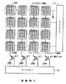
先ず、図10及び図10の一部を拡大して示した図11を参照して説明する。この従来例の平面型表示装置は、マトリックス状に配されたm行n列(但し、m、nは1以上の整数で、ここではm=5、n=4であるが、実際には、例えば、m=40、n=25である)の電界放出型カソードKからなる画素が、M行N列(但し、M、Nは2以上の整数)のマトリックス状に配列された電界放出型カソード群と、M行N列のマトリックス状に配列された画素にそれぞれ対応するM行N列のマトリックス状に配された引き出し電極DRからなる引き出し電極群と、その引き出し電極群に対向するアノード電極(図示を省略)と、そのアノード電極の上側又は下側に設けられた蛍光体層(図示を省略)と、引き出し電極群に対し行毎に順次に循環的に引き出し電圧を印加するスキャンドライバSDと、電界放出型カソード群に対し画素の列毎に画像データに応じて選択的に低電圧を印加するデータドライバDDとを有する。
【0017】
画素毎の電界放出型カソードKは、それぞれカソード電極KK上に植立され、画素毎の電界放出型カソードKに対応する各引き出し電極DRには、その各カソードKに対応する孔hが穿設されている。画素毎の電界放出型カソードK及びそれに対応する引き出し電極DRの間には、図示を省略するも絶縁層(例えば、SiO2)が介在せしめられ、その絶縁層には、引き出し電極DRの各孔hに連通するキャビティ(図示せず)が設けられている。
【0018】
電界放出型カソードKは、例えば、円錐形形状のスピント( Spindt:人名) 型で、0.01V/Å〜0.1V/Å程度の電界を選択的に与えることによって、トンネル効果により電子放出がなされる、Mo、W、Cr等の材料から構成される。そして、カソードKの頂点が孔hの中心に対応するように、孔h及びカソードK間の位置関係が設定されている。
【0019】
全画面共通のアノード電極には、例えば、+3〜+5kV程度の固定の高圧直流電圧が印加される。列毎の複数の引き出し電極DRには、スキャンドライバSDからの、例えば、+100Vの直流電圧が、それぞれ行線Cを通じて上側の引き出し電極DRの列から下側の引き出し電極DRの列へと順次循環的に印加される。各列の画素毎のカソードKには、データドライバDDからの、画像信号に応じた0V(例えば、0V〜+10Vの電圧も可)の電圧が、それぞれ列線R及び各列のカソード電極KKを通じて印加される。
【0020】
かくして、複数行の引き出し電極DR及びカソード電極Kの複数列の画素のうち、+100Vの直流電圧が印加さされた引き出し電極DRの列と、0Vの電圧が印加された列の画素のカソードKの交点において、引き出し電極DRによって、1画素分のカソードKから引き出された電子が、アノード電極によって引っ張られて電界放射(電子放射)が開始され、アノード電極の1画素分のカソードKに対向する部分が電子によって衝撃されて、その部分の蛍光体層が発光して、1画素分の画像が表示される。
【0021】
蛍光体層の全体を、白色発光蛍光体層にて構成すれば、モノクローム平面型表示装置が得られ、蛍光体層を1画素毎の幅を有する赤、緑及び青発光蛍光体ストライプにて構成すれば、カラー平面型表示装置が得られる。
【0022】
これらの引き出し電極DR、カソード電極KK、カソードK、アノード電極、蛍光体層及び絶縁層が、ガラス等からなる偏平管内に収納され、偏平管内は高真空となされる。
【0023】
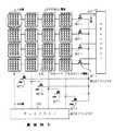
図11において、MTは、各カソード電極KK及び各電界放出型カソードK間に接続されたnチャンネル型のMOSトランジスタで、その断面構造を図12に示す。SBはp型の基板、Dはn+型のドレイン、Sは同じくn+型のソース、INは絶縁層、Gはゲート電極である。MOSトランジスタMTのドレインがカソードKに接続され、そのソースがカソード電極KK(図12では図示を省略している)に接続される。このMOSトランジスタMTのゲートに、所定の固定電圧が印加されて、MOSトランジスタMTがオンになされると共に、カソード電極KKに、例えば、接地電位が与えられると共に、そのカソード電極KKと交叉する引き出し電極DRに、例えば、+100Vの電圧が与えられたとき、そのカソード電極KK及び引き出し電極DRの交叉部の画素を構成する各カソードKからアノード電極に流れる電子流、即ち、アノード電極からカソードKに流れる放射電流が、図13の曲線▲2▼に示す如く引き出し電極DRに印加される電圧の上昇にも拘らず、一定値に抑えられる。尚、図13の▲1▼は、MOSトランジスタを設けない場合の放射電流の特性を示し、引き出し電極の電圧の増加に伴って無限大に近く上昇する。
【0024】
【発明が解決しようとする課題】
図10及び図11に示した従来例の平面型表示装置では、データドライバの駆動電流が大きくなり、データドライバの負担が大きくなるという欠点がある。又、各電界放出型カソードに対し、個別にMOSトランジスタを設けるので、構造が複雑になると共に、製造工程が複雑になる。
【0025】
かかる点に鑑み、本発明は、アノード電極及び電界放出型カソード間の放射電流の上限を、安定に一定に抑えることができると共に、データ駆動手段の負担を小さくすることができ、且つ、電力消費の増大を抑制することのできる平面型表示装置を提案しようとするものである。
【0026】
又、本発明は、アノード電極及び画素を構成する複数の電界放出型カソード間の放射電流の上限を、安定に一定に抑えることができると共に、データ駆動手段の負担を小さくすることができ、電力消費の増大を抑制することができ、且つ、構造及び製造工程が簡単となる平面型表示装置を提案しようとするものである。
【0027】
更に、本発明は、アノード電極及び画素を構成する複数の電界放出型カソード間の放射電流の上限を、安定に一定に抑えることができると共に、電力消費の増大を抑制することができ、且つ、構造及び製造工程が簡単となる平面型表示装置を提案しようとするものである。
【0028】
更に、本発明は、アノード電極及び画素を構成する複数の電界放出型カソード間の放射電流の上限を、安定に一定に抑えることができると共に、電力消費の増大を抑制することができ、データ駆動手段の負担を小さくすることができ、且つ、構造及び製造工程が簡単となる平面型表示装置を提案しようとするものである。
【0029】
【課題を解決するための手段】
上記課題を解決するために、本発明の平面型表示装置は、マトリックス状に配されたm行n列(但し、m、nは1以上の整数)の電界放出型カソードからなる画素が、M行N列(但し、M、Nは2以上の整数)のマトリックス状に配列された電界放出型カソード群と、M行N列のマトリックス状に配列された画素にそれぞれ対応するM行N列のマトリックス状に配された引き出し電極からなる引き出し電極群と、引き出し電極群に対向するアノード電極と、アノード電極に設けられた蛍光体層と、引き出し電極群に対し行毎に順次に循環的に引き出し電圧を印加する走査駆動手段と、各電界放出型カソード及び低電圧点間にそれぞれ接続された定電流手段からなる定電流手段群と、定電流手段群のうち、走査駆動手段によって選択された行の定電流手段の集合体について、画像データに応じて、定電流動作状態又は高インピーダンス状態のいずれかに制御するデータ駆動手段とを有する。
【0030】
かかる本発明によれば、データ駆動手段は、画像データに応じて、各電界放出型カソード電極及び低電圧点間にそれぞれ接続された定電流手段からなる定電流手段群を、画素の列毎に選択的に定電流動作状態に制御すると共に、残りを高インピーダンス状態に制御する。
【0035】
【発明の実施の形態】
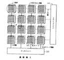
〔発明の実施の形態の具体例〕以下に、図1及びその一部の拡大図である図2を参照して、本発明の実施の形態の具体例1の平面型表示装置を説明する。この具体例1の平面型表示装置は、マトリックス状に配されたm行n列(但し、m、nは1以上の整数で、ここではm=5、n=4であるが、実際には、例えば、m=40、n=25である)の電界放出型カソードKからなる画素が、M行N列(但し、M、Nは2以上の整数)のマトリックス状に配列された電界放出型カソード群と、M行N列のマトリックス状に配列された画素にそれぞれ対応するM行N列のマトリックス状に配された引き出し電極DRからなる引き出し電極群と、その引き出し電極群に対向するアノード電極(図示を省略)と、そのアノード電極の上側又は下側に設けられた蛍光体層(図示を省略)と、引き出し電極群に対し行毎に順次に循環的に引き出し電圧を印加するスキャンドライバSDと、電界放出型カソード群に対し画素の列毎に画像データに応じて選択的に低電圧を印加するデータドライバDDとを有する。
【0036】
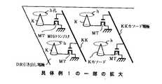
図2に示す如く、電界放出型カソードKに対応する各引き出し電極DRには、その各カソードKに対応する孔hが穿設されている。電界放出型カソードK及びそれに対応する引き出し電極DRの間には、図示を省略するも絶縁層(例えば、SiO2)が介在せしめられ、その絶縁層には、引き出し電極DRの各孔hに連通するキャビティ(図示せず)が設けられている。
【0037】
電界放出型カソードKは、例えば、円錐形形状のスピント( Spindt:人名) 型で、0.01V/Å〜0.1V/Å程度の電界を選択的に与えることによって、トンネル効果により電子放出がなされる、Mo、W、Cr等の材料から構成される。そして、カソードKの頂点が孔hの中心に対応するように、孔h及びカソードK間の位置関係が設定されている。
【0038】
全画面共通のアノード電極(図示を省略)には、例えば、+3〜+5kV程度の固定の高圧直流電圧が印加される。図1に示す如く、列毎の複数の引き出し電極DRには、スキャンドライバSDからの、例えば、+100Vの直流電圧が、それぞれ行線Cを通じて上側の引き出し電極DRの列から下側の引き出し電極DRの列へと順次循環的に印加される。
【0039】
図2において、MTは、各カソード電極KK及び各電界放出型カソードK間に接続されたnチャンネル型のMOSトランジスタで、MOSトランジスタMTのドレインがカソードKに接続され、そのソースが接地され、そのゲートがカソード電極KKに接続される。このMOSトランジスタMTのゲートに、データドライバDDによって、画像データに応じて、例えば、+5Vの電圧が選択的に印加されたときは、MOSトランジスタMTがオンになって、カソードKに接地電位が与えられる。このとき、このカソードKの画素に対応する引き出し電極DRに、例えば、+100Vの電圧が印加されているときは、カソードKからアノード電極に電子が放射されて、電子によって衝撃されたアノード電極の部分の蛍光体層が発光する。又、MOSトランジスタMTのゲートに、データドライバDDによって、画像データに応じて、例えば、0Vの電圧が選択的に印加されたときは、MOSトランジスタMTはオフとなり(高インピーダンスを呈する)、カソードKの電位は浮いたままである。このときは、このカソードKの画素に対応する引き出し電極DRに、+100Vの電圧が印加されていても、カソードKからアノード電極への電子の放射は行われない。
【0040】
かくして、複数行の引き出し電極DR及びカソード電極Kの複数列の画素のうち、+100Vの直流電圧が印加さされた引き出し電極DRの列と、0Vの電圧が印加された列の画素のカソードKの交点において、引き出し電極DRによって、1画素分のカソードKから引き出された電子が、アノード電極によって引っ張られて電界放射(電子放射)が開始され、アノード電極の1画素分のカソードKに対向する部分が電子によって衝撃されて、その部分の蛍光体層が発光して、1画素分の画像が表示される。
【0041】
蛍光体層の全体を、白色発光蛍光体層にて構成すれば、モノクローム平面型表示装置が得られ、蛍光体層を1画素毎の幅を有する赤、緑及び青発光蛍光体ストライプにて構成すれば、カラー平面型表示装置が得られる。
【0042】
これらの引き出し電極DR、カソード電極KK、カソードK、MOSトランジスタMTアノード電極、蛍光体層及び酸化膜が、ガラス等からなる偏平管内に収納され、偏平管内は高真空となされる。
【0043】
図1及び図2に示した具体例1の平面型表示装置によれば、MOSトランジスタMTによって、アノード電極及び電界放出型カソードK間の放射電流の上限を、安定に一定に抑えることができると共に、アノード電極及びカソードK間の放射電流がデータドライバに流れないので、データドライバDDの負担を小さくすることができ、且つ、定電流を得るための高抵抗器を用いないので、電力消費の増大を抑制することのできる。
【0044】
次に、図3を参照して、本発明の実施の形態の具体例2の平面型表示装置を説明するも、図1と対応する部分には、同一符号を付して一部重複説明を省略する。この具体例2の平面型表示装置は、マトリックス状に配されたm行n列(但し、m、nは1以上の整数、ここではm=5、n=4、実際には、例えば、m=40、n=25である)の電界放出型カソードKからなる画素が、M行N列(但し、M、Nは2以上の整数)のマトリックス状に配列された電界放出型カソード群と、M行N列のマトリックス状に配列された画素にそれぞれ対応するM行N列のマトリックス状に配された引き出し電極DRからなる引き出し電極群と、その引き出し電極群に対向するアノード電極(図示を省略)と、そのアノード電極に設けられた蛍光体層(図示を省略)と、引き出し電極群に対し行毎に順次に循環的に引き出し電圧を印加するスキャンドライバSDと、電界放出型カソード群に対し画素の列毎に画像データに応じて選択的に低電圧を印加するデータドライバDDとを有する。
【0045】
そして、この平面型表示装置は、電界放出型カソード群に対し画素の列毎に低電圧点との間にそれぞれ接続されたMOSトランジスタMTを有し、データドライバDDは、画像データに応じて、N個のMOSトランジスタMTを選択的に定電流動作状態に制御すると共に、残りを高インピーダンス状態に制御するようにする。即ち、MOSトランジスタMTの各ドレインを、列線R及びカソード電極KKを通じて、カソードKの画素の列に接続し、その各ソースを接地し、その各ゲートをデータドライバDDに接続する。
【0046】
データドライバDDは、各MOSトランジスタMTに対し、画像データに応じて、+5V及び0Vの電圧を選択的に印加する。スキャンドライバSDは、引き出し電極DRに対し、行毎に順次に循環的に、行線Cを通じて、例えば、+100Vの電圧を印加する。
【0047】
MOSトランジスタMTのゲートに、データドライバDDによって、画像データに応じて、例えば、+5Vの電圧が選択的に印加されたときは、MOSトランジスタMTがオンになって、カソードKに接地電位が与えられる。このとき、このカソードKの画素に対応する引き出し電極DRに、例えば、+100Vの電圧が印加されているときは、カソードKからアノード電極に電子が放射されて、電子によって衝撃されたアノード電極の部分の蛍光体層が発光する。又、MOSトランジスタMTのゲートに、データドライバDDによって、画像データに応じて、例えば、0Vの電圧が選択的に印加されたときは、MOSトランジスタMTはオフとなり(高インピーダンスを呈する)、カソードKの電位は浮いたままである。このときは、このカソードKの画素に対応する引き出し電極DRに、+100Vの電圧が印加されていても、カソードKからアノード電極への電子の放射は行われない。
【0048】
この図3に示した具体例2の平面型表示装置によれば、MOSトランジスタMTによって、アノード電極及び画素を構成する複数の電界放出型カソード間の放射電流の上限を、安定に一定に抑えることができると共に、データドライバDDにアノード電極及びカソードK間の放射電流が流れないので、データドライバの負担を小さくすることができ、定電流を得るための高抵抗器を用いないので、電力消費の増大を抑制することができ、且つ、MOSトランジスタを電界照射型カソードK群の画素の列毎に設けるので、構造及び製造工程が簡単となる平面型表示装置を得ることができる。アノード電極及び画素を構成する複数の電界放出型カソード間の放射電流の上限を、安定に一定に抑えることができるということは、換言すれば、画素を構成する複数の電界放出型カソードのうちの1部のカソードから電子が放射されなくとも、又、1個のカソードのみから電子が放出されても、アノード電極及び画素を構成する複数の電界放出型カソード間のトータルの放射電流の上限は、安定に一定に抑えられるということである。
【0049】
次に、図4を参照して、本発明の実施の形態の具体例3の平面型表示装置を説明するも、図1と対応する部分には、同一符号を付して一部重複説明を省略する。この具体例3の平面型表示装置は、マトリックス状に配されたm行n列(但し、m、nは1以上の整数で、ここではm=5、n=4、実際には、例えば、m=40、n=25である)の電界放出型カソードKからなる画素が、M行N列(但し、M、Nは2以上の整数)のマトリックス状に配列された電界放出型カソード群と、M行N列のマトリックス状に配列された画素にそれぞれ対応するM行N列のマトリックス状に配された引き出し電極DRからなる引き出し電極群と、その引き出し電極群に対向するアノード電極(図示を省略)と、そのアノード電極に設けられた蛍光体層(図示を省略)と、引き出し電極群に対し行毎に順次に循環的に引き出し電圧を印加するスキャンドライバSDと、電界放出型カソード群に対し画素の列毎に画像データに応じて選択的に低電圧を印加するデータドライバDDとを有する。
【0050】
そして、この平面型表示装置は、電界放出型カソード群に対し画素の列毎にデータドライバDDとの間にそれぞれ接続された常時定電流状態にあるMOSトランジスタを有する。即ち、MOSトランジスタMTの各ドレインを、列線R及びカソード電極KKを通じて、カソードKの画素の列に接続し、その各ソースをデータドライバDDに接続し、その各ゲートに、入力端子tから、例えば、+5Vの固定直流電圧を印加して、常時オン状態にしておく。
【0051】
MOSトランジスタMTのソースに、データドライバDDによって、画像データに応じて、例えば、0Vの電圧が選択的に印加されたときは、画素を構成する複数のカソードKの列毎に、接地電位が与えられる。このとき、この画素を構成する複数のカソードKに対応する引き出し電極DRに、例えば、+100Vの電圧が印加されているときは、カソードKからアノード電極に電子が放射されて、電子によって衝撃されたアノード電極の部分の蛍光体層が発光する。又、MOSトランジスタMTのゲートに、データドライバDDによって、画像データに応じて、選択的に何らの電圧も与えられないときは、カソードKの電位は浮いたままである。このときは、この画素を構成する複数のカソードKに対応する引き出し電極DRに、+100Vの電圧が印加されていても、カソードKからアノード電極への電子の放射は行われない。
【0052】
図4に図示の具体例3の平面型表示装置によれば、MOSトランジスタMTによって、アノード電極及び画素を構成する複数の電界放出型カソード間の放射電流の上限を、安定に一定に抑えることができると共に、定電流を得るための高抵抗器を用いないので、電力消費の増大を抑制することができ、且つ、MOSトランジスタを、画素を構成する複数のカソードKの列毎に設けるので、構造及び製造工程が簡単となる平面型表示装置を得ることができる。
【0053】
次に、図5を参照して、具体例4の平面型表示装置を説明する。この平面型表示装置では、データドライバDDと、カソード電極Kの画素の列との間に、定電流供給回路CISを設けた場合である。この定電流供給回路CISは、図3又は図4に類似した画素を構成する複数の電界放出型カソードの画素の列毎のバイポーラトランジスタ等の半導体素子よりなる定電流手段から構成される。その他の構成は、図3又は図4と同様である。
【0054】
この図5に図示の平面型表示装置によれば、定電流手段によって、アノード電極及び画素を構成する複数の電界放出型カソード間の放射電流の上限を、安定に一定に抑えることができると共に、定電流化のための高抵抗器を用いないので、電力消費の増大を抑制することができ、画素を構成する複数の電界放射型カソードKの列毎に、定電流供給器を設けるので、構造が簡単で製造の容易な平面型表示装置を得ることができる。
【0055】
次に、図6を参照して、本発明の実施の形態の具体例4の平面型表示装置を説明するも、図1と対応する部分には同一符号を付して、一部重複説明を省略する。この具体例4の平面型表示装置は、マトリックス状に配されたm行n列(但し、m、nは1以上の整数で、ここでは、m=5、n=4、実際には、例えば、m=40、n=25)の電界放出型カソードKからなる画素が、M行N列(但し、M、Nは2以上の整数)のマトリックス状に配列された電界放出型カソード群と、M行N列のマトリックス状に配列された画素にそれぞれ対応するM行N列のマトリックス状に配された引き出し電極DRからなる引き出し電極群と、その引き出し電極群に対向するアノード電極(図示を省略)と、そのアノード電極に設けられた蛍光体層(図示を省略)とを有する。
【0056】
そして、この平面型表示装置は、引き出し電極DRに対し列毎に画像データに応じて選択的に引き出し電圧を印加するデータドライバDDと、電界放出型カソード群に対し画素の行毎にそれぞれ一端が接続されたM個の第1の定電流手段MT1と、そのM個の第1の定電流手段MT1を順次に循環的に定電流動作状態に制御すると共に、残りを高インピーダンス状態に制御するスキャンドライバSDと、データドライバDDによって、画像データに応じて、選択的に定電流動作状態に制御されると共に、残りは高インピーダンス状態に制御される、各一端が接地に接続され、各他端がM個の第1の定電流手段MT1の各他端に共通に接続されたN個の第2の定電流手段MT2とを有する。
【0057】
即ち、各MOSトランジスタMT1のドレインが、画素に対応する複数のドレインが引き出し電極DRの行に接続され、その各ゲートが列線Cを通じてスキャンドライバSDに接続され、そのドレイン他のMOSトランジスタMT1のドレインとそれぞれと共通接続される。又、各MOSトランジスタMT2のゲートが、データドライバDDの列線R及び画素を構成する複数の電界放出型カソードKの列に接続され、その各ソースが接地され、その各ドレインが他のMOSトランジスタMT2のドレインと共通接続されると共に、各MOSトランジスタMT1のソースに共通に接続される。
【0058】
ある列線Rに接続された、画素に対応する引き出し電極DRの列に、データドライバからの+100Vの電圧が印加されると共に、ある行線CのMOSトランジスタMT2ゲートに、スキャンドライバSDからの+5Vの電圧が印加されると、そのある行線Cにゲートが接続されがMOSトランジスタMT1がオンになると共に、そのある列線Rにゲートが接続されたMOSトランジスタMT2もオンになり、そのある行線Cにゲートが接続されたMOSトランジスタMT1のソース側に接地電位が与えられて、そのある行及びそのある列の交点の画素を構成する複数のカソードKが電子を放出してアノード電極との間で電界放出が行われると共に、その画素の放射電流の上限が、MOSトランジスタMT1、MT2の直列回路によって、所定の一定値に抑えられる。
【0059】
この図6の第5の具体例にによれば、データドライバDDに照射電流がながれないので、データドライバDDの負担を小さくすることができ、定電流を得るための高抵抗器を使用しないので、消費電力の増大が抑制されると共に、アノード電極及び画素を構成する複数の電界放出型カソード間の放射電流の上限を、安定に一定に抑えることができると共に、画素を構成する複数お電界放出型カソードKの行及び画素に対応する引き出し電極DRの列にMOSトランジスタMT1、MT2が接続されるので、構造及び製造工程が簡単となり、しかも、同じ行又は同じ列における表示状態となる画素数が多くなる場合に、各画素の放射電流の減少を緩和することができる。
【0060】
上述の各具体例においては、nチャンネル型MOSトランジスタを用いた場合ついて述べたが、pチャンネル型MOSトランジスタを用いることもできる。
【0061】
【発明の効果】
本発明によれば、マトリックス状に配されたm行n列(但し、m、nは1以上の整数)の電界放出型カソードからなる画素が、M行N列(但し、M、Nは2以上の整数)のマトリックス状に配列された電界放出型カソード群と、M行N列のマトリックス状に配列された画素にそれぞれ対応するM行N列のマトリックス状に配された引き出し電極からなる引き出し電極群と、その引き出し電極群に対向するアノード電極と、そのアノード電極に設けられた蛍光体層と、引き出し電極群に対し行毎に順次に循環的に引き出し電圧を印加する走査駆動手段と、電界放出型カソード群に対し画素の列毎に画像データに応じて選択的に低電圧を印加するデータ駆動手段とを有する平面型表示装置において、各電界放出型カソード電極及び低電圧点間にそれぞれ接続された定電流手段からなる定電流手段群を設けてなり、データ駆動手段は、画像データに応じて、定電流手段群を画素の列毎に選択的に定電流動作状態に制御すると共に、残りを高インピーダンス状態に制御するようにしたので、アノード電極及び電界放出型カソード間の放射電流の上限を、安定に一定に抑えることができると共に、データ駆動手段の負担を小さくすることができ、且つ、電力消費の増大を抑制することのできる平面型表示装置を得ることができる。
【図面の簡単な説明】
【図1】本発明の実施の形態の具体例1の平面型表示装置を示すブロック線図である。
【図2】具体例1の一部の拡大接続図である。
【図3】本発明の実施の形態の具体例2の平面型表示装置を示すブロック線図である。
【図4】本発明の実施の形態の具体例3の平面型表示装置を示すブロック線図である。
【図5】本発明の実施の形態の具体例4の平面型表示装置を示すブロック線図である。
【図6】本発明の実施の形態の具体例5の平面型表示装置を示すブロック線図である。
【図7】従来の平面型表示装置の一部を示す平面図である。
【図8】従来の平面型表示装置の一部の断面図である。
【図9】平面型表示装置のカソードの例を示す平面図及び断面図である。
【図10】従来例の平面型表示装置を示すブロック線図である。
【図11】従来例の平面型表示装置の一部の拡大接続図である。
【図12】従来例の平面型表示装置のカソードとMOSトランジスタとの組み合わせ部分を示す断面図である。
【図13】従来例の引き出し電圧と放射電流との間の関係を示す特性曲線図である。
【符号の説明】
K 電界放出型カソード、KK カソード電極、DR 引き出し電極、h 孔、DD データドライバ、SD スキャンドライバ。[0001]
BACKGROUND OF THE INVENTION
The present invention relates to a flat display device provided with a field emission cathode.
[0002]
[Prior art]
Hereinafter, a conventional example of a flat display device provided with a field emission cathode (emitter) will be described with reference to FIGS. In FIG. 7 and FIG. 8, KK and G are a plurality of equally spaced cathode electrodes and gate electrodes (leading electrodes) constituting the XY matrix, respectively, and cross each other across the insulating layer Z. It is arranged like this. A is an anode electrode facing a plurality of gate electrodes G with a predetermined interval. A phosphor layer P is applied to the upper surface (or lower surface) of the anode electrode A.
[0003]
At the intersection of the plurality of cathode electrodes KK and the plurality of gate electrodes G, each gate electrode G is provided with a circular hole h, and a cavity CV communicating with the hole h is provided in the insulating layer Z. In this cavity CV, a conical spindt (person name) field emission cathode (emitter) K is planted on the cathode electrode KK. The field emission cathode K is made of a material such as Mo, W, or Cr that emits electrons by a tunnel effect by selectively applying an electric field of about 0.01 V / Å to 0.1 V / Å. . The positional relationship between the hole h and the cathode K is set so that the vertex of the cathode K is located at the center of the hole h.
[0004]
These electrode G, cathode electrode KK, cathode K, anode electrode A, phosphor layer P and insulating layer Z are housed in a flat tube made of glass or the like, and the flat tube is evacuated.
[0005]
A fixed voltage, for example, a DC voltage of +3 kV is applied to the anode electrode A. For example, a +100 V DC voltage from the scan driver SD is sequentially and cyclically applied to the plurality of gate electrodes G from the upper gate electrode G to the lower gate electrode G in FIG. A voltage of 0 V (for example, a voltage of 0 V to +10 V is also acceptable) from the data driver DD according to the image signal is selectively applied to the plurality of cathode electrodes KK.
[0006]
Thus, among the plurality of gate electrodes G and the plurality of cathode electrodes KK, the cathode K and the anode electrode A at the intersection of the gate electrode G to which a direct voltage of +100 V is applied and the cathode electrode KK to which a voltage of 0 V is applied. Then, field emission (electron emission) is started, and electrons extracted from the cathode K by the gate electrode G are bombarded by the anode electrode A, and the phosphor layer P emits light.
[0007]
In this flat display device, an image is displayed with, for example, a collection of 1000 intersections of the gate electrode G and the cathode electrode KK as one pixel. If the entire phosphor layer P is composed of a white light emitting phosphor layer, a monochrome flat display device can be obtained, and the phosphor layer P is formed of red, green and blue light emitting phosphor stripes having a width for each pixel. In this way, a color flat display device can be obtained.
[0008]
There are various examples of the field emission cathode (emitter) K in addition to those shown in FIG. 8, and some examples will be described with reference to FIG. 9A1, B1, and C1 are plan views of the cathode, and FIGS. 9A2, B2, and C2 are cross-sectional views of the cathode of FIGS. 9A1, B1, and C1, respectively.
[0009]
9A1 and 9A2 show a pair of electrodes, one of which is a cathode and the other is a gate electrode, and electrons are emitted from an end portion facing the gate electrode of the cathode toward an anode electrode (not shown). Note that either one or both of the pair of electrodes may have a comb shape.
[0010]
9B1 and 9B2 show, for example, a cathode having a square hole, and electrons are emitted from the edge of the square hole.
[0011]
9C1 and 9C2 illustrate a cathode in which the upper surface of the disk is recessed so as to form a curved surface, for example, a spherical surface, and electrons are emitted from the edge of the recess.
[0012]
As an example of the field emission cathode (emitter) K, an MIM type electron-emitting device made of metal / insulating layer / metal may be used.
[0013]
In a flat display device having such a field emission type cathode, although not shown in the drawing, a high resistance resistor of about 1 MΩ, for example, is connected between each cathode K and each cathode electrode KK. Thus, the radiation current from each cathode K is stabilized.
[0014]
However, in this case, since a current flows through a high-resistance resistor, this increases power consumption in the flat display device, which is not preferable.
[0015]
Next, referring to FIGS. 10 to 13, by using a MOS transistor, the emission current from each cathode is stabilized without increasing the power consumption in the flat display device. Another conventional example will be described.
[0016]
First, a description will be given with reference to FIG. 10 and FIG. 11 showing an enlarged part of FIG. This conventional flat display device has m rows and n columns arranged in a matrix (where m and n are integers of 1 or more, where m = 5 and n = 4, but in practice, For example, a field emission cathode in which pixels of a field emission cathode K of m = 40 and n = 25 are arranged in a matrix of M rows and N columns (where M and N are integers of 2 or more). A group of extraction electrodes composed of extraction electrodes DR arranged in a matrix of M rows and N columns respectively corresponding to pixels arranged in a matrix of M rows and N columns, and an anode electrode ( (Not shown), a phosphor layer (not shown) provided on the upper side or the lower side of the anode electrode, and a scan driver SD for cyclically applying a lead-out voltage to the lead-out electrode group sequentially in rows. In field emission cathode group In selectively in accordance with image data for each column of pixels and a data driver DD for applying a low voltage.
[0017]
A field emission cathode K for each pixel is planted on the cathode electrode KK, and a hole h corresponding to each cathode K is formed in each extraction electrode DR corresponding to the field emission cathode K for each pixel. Has been. An insulating layer (for example, SiO 2) is omitted between the field emission cathode K for each pixel and the corresponding extraction electrode DR.2) And cavities (not shown) communicating with the respective holes h of the extraction electrode DR are provided in the insulating layer.
[0018]
The field emission cathode K is, for example, a cone-shaped Spindt type, and by selectively applying an electric field of about 0.01 V / Å to 0.1 V / Å, electron emission is caused by a tunnel effect. It is made of a material such as Mo, W, or Cr. The positional relationship between the hole h and the cathode K is set so that the vertex of the cathode K corresponds to the center of the hole h.
[0019]
For example, a fixed high DC voltage of about +3 to +5 kV is applied to the anode electrode common to all screens. For example, + 100V DC voltage from the scan driver SD is sequentially circulated through the row line C from the column of the upper extraction electrode DR to the column of the lower extraction electrode DR through the plurality of extraction electrodes DR for each column. Applied. A voltage of 0 V (for example, a voltage of 0 V to +10 V is also possible) corresponding to the image signal from the data driver DD is applied to the cathode K for each pixel of each column through the column line R and the cathode electrode KK of each column. Applied.
[0020]
Thus, among the pixels in the plurality of columns of the extraction electrodes DR and the cathode electrodes K in a plurality of rows, the column of the extraction electrode DR to which a direct voltage of +100 V is applied and the cathode K of the pixel in the column to which a voltage of 0 V is applied. At the intersection, electrons extracted from the cathode K for one pixel by the extraction electrode DR are pulled by the anode electrode to start field emission (electron emission), and a portion of the anode electrode facing the cathode K for one pixel Is bombarded with electrons, and the phosphor layer in that portion emits light, and an image for one pixel is displayed.
[0021]
If the entire phosphor layer is composed of a white light emitting phosphor layer, a monochrome flat display device can be obtained, and the phosphor layer is composed of red, green and blue light emitting phosphor stripes each having a width of one pixel. Then, a color flat display device can be obtained.
[0022]
These lead electrode DR, cathode electrode KK, cathode K, anode electrode, phosphor layer and insulating layer are accommodated in a flat tube made of glass or the like, and the flat tube is evacuated.
[0023]
11, MT is an n-channel MOS transistor connected between each cathode electrode KK and each field emission cathode K, and its cross-sectional structure is shown in FIG. SB is a p-type substrate, D is n+Type drain, S is also n+The source of the mold, IN is an insulating layer, and G is a gate electrode. The drain of the MOS transistor MT is connected to the cathode K, and the source is connected to the cathode electrode KK (not shown in FIG. 12). A predetermined fixed voltage is applied to the gate of the MOS transistor MT, the MOS transistor MT is turned on, and, for example, a ground potential is applied to the cathode electrode KK, and an extraction electrode that intersects the cathode electrode KK. For example, when a voltage of +100 V is applied to DR, an electron flow flows from each cathode K constituting the pixel at the intersection of the cathode electrode KK and the extraction electrode DR to the anode electrode, that is, flows from the anode electrode to the cathode K. As shown by the curve (2) in FIG. 13, the radiation current is suppressed to a constant value regardless of the increase in the voltage applied to the extraction electrode DR. Incidentally, (1) in FIG. 13 shows the characteristics of the radiation current when no MOS transistor is provided, and it rises near infinity as the voltage of the extraction electrode increases.
[0024]
[Problems to be solved by the invention]
The conventional flat display device shown in FIGS. 10 and 11 has a drawback that the drive current of the data driver becomes large and the burden on the data driver becomes large. Further, since MOS transistors are individually provided for each field emission cathode, the structure becomes complicated and the manufacturing process becomes complicated.
[0025]
In view of this point, the present invention can stably keep the upper limit of the radiation current between the anode electrode and the field emission cathode, can reduce the burden on the data driving means, and can consume power. Therefore, the present invention intends to propose a flat display device capable of suppressing the increase of the above.
[0026]
In addition, the present invention can stably and constantly suppress the upper limit of the emission current between the plurality of field emission cathodes constituting the anode electrode and the pixel, and can reduce the burden on the data driving means. An object of the present invention is to propose a flat display device that can suppress an increase in consumption and that has a simple structure and manufacturing process.
[0027]
Furthermore, the present invention can stably suppress the upper limit of the emission current between the plurality of field emission cathodes constituting the anode electrode and the pixel, can suppress an increase in power consumption, and An object of the present invention is to propose a flat display device having a simple structure and manufacturing process.
[0028]
Furthermore, according to the present invention, the upper limit of the emission current between the plurality of field emission cathodes constituting the anode electrode and the pixel can be stably suppressed to a constant value, and an increase in power consumption can be suppressed. An object of the present invention is to propose a flat display device that can reduce the burden on the means and that has a simple structure and manufacturing process.
[0029]
[Means for Solving the Problems]
In order to solve the above-described problem, a flat display device according to the present invention includes a pixel having a field emission cathode of m rows and n columns (where m and n are integers of 1 or more) arranged in a matrix. Field emission cathode groups arranged in a matrix of rows and N columns (where M and N are integers of 2 or more), and M rows and N columns corresponding to pixels arranged in a matrix of M rows and N columns, respectively. A lead-out electrode group composed of lead-out electrodes arranged in a matrix, an anode electrode facing the lead-out electrode group, a phosphor layer provided on the anode electrode, and the lead-out electrode group are sequentially and cyclically drawn out row by row. Scanning drive means for applying a voltage;Each field emission cathodeAnd a set of constant current means connected to each other between the low voltage points, and a set of constant current means in a row selected by the scanning drive means in the constant current means group according to the image data. And data driving means for controlling to either a constant current operation state or a high impedance state.
[0030]
According to the present invention,The data driving means selectively operates a constant current means group consisting of constant current means connected between each field emission type cathode electrode and a low voltage point for each pixel column according to image data. Control to the state and the rest to the high impedance state.
[0035]
DETAILED DESCRIPTION OF THE INVENTION
[Specific Example of Embodiment of the Invention] A flat display device according to a specific example 1 of the embodiment of the present invention will be described below with reference to FIG. 1 and FIG. 2 which is an enlarged view of a part thereof. The flat display device of Example 1 has m rows and n columns arranged in a matrix (where m and n are integers of 1 or more, where m = 5 and n = 4. (For example, m = 40, n = 25) field emission type cathodes K are arranged in a matrix of M rows and N columns (where M and N are integers of 2 or more). Cathode group, extraction electrode group consisting of extraction electrodes DR arranged in a matrix of M rows and N columns, respectively corresponding to pixels arranged in a matrix of M rows and N columns, and an anode electrode facing the extraction electrode group (Not shown), a phosphor layer (not shown) provided on the upper or lower side of the anode electrode, and a scan driver SD that applies an extraction voltage in a cyclic manner sequentially for each row to the extraction electrode group. And field emission cathodes Optionally according to the image data for each column of against pixels and a data driver DD for applying a low voltage.
[0036]
As shown in FIG. 2, each extraction electrode DR corresponding to the field emission type cathode K is provided with a hole h corresponding to each cathode K. An insulating layer (for example, SiO 2) is omitted between the field emission cathode K and the corresponding extraction electrode DR.2) And cavities (not shown) communicating with the respective holes h of the extraction electrode DR are provided in the insulating layer.
[0037]
The field emission cathode K is, for example, a cone-shaped Spindt type, and by selectively applying an electric field of about 0.01 V / Å to 0.1 V / Å, electron emission is caused by a tunnel effect. It is made of a material such as Mo, W, or Cr. The positional relationship between the hole h and the cathode K is set so that the vertex of the cathode K corresponds to the center of the hole h.
[0038]
For example, a fixed high voltage DC voltage of about +3 to +5 kV is applied to an anode electrode (not shown) common to all screens. As shown in FIG. 1, a DC voltage of, for example, + 100V from the scan driver SD is applied to the plurality of extraction electrodes DR for each column from the column of the upper extraction electrode DR through the row line C, respectively. Are sequentially and cyclically applied to the columns.
[0039]
In FIG. 2, MT is an n-channel MOS transistor connected between each cathode electrode KK and each field emission cathode K. The drain of the MOS transistor MT is connected to the cathode K, its source is grounded, The gate is connected to the cathode electrode KK. For example, when a voltage of +5 V is selectively applied to the gate of the MOS transistor MT by the data driver DD according to the image data, the MOS transistor MT is turned on and a ground potential is applied to the cathode K. It is done. At this time, when a voltage of, for example, +100 V is applied to the extraction electrode DR corresponding to the pixel of the cathode K, a part of the anode electrode radiated from the cathode K to the anode electrode and bombarded by the electrons The phosphor layer emits light. When a voltage of, for example, 0V is selectively applied to the gate of the MOS transistor MT by the data driver DD according to the image data, the MOS transistor MT is turned off (exhibits high impedance), and the cathode K The potential remains floating. At this time, even if a voltage of +100 V is applied to the extraction electrode DR corresponding to the pixel of the cathode K, electrons are not emitted from the cathode K to the anode electrode.
[0040]
Thus, among the pixels in the plurality of columns of the extraction electrodes DR and the cathode electrodes K in a plurality of rows, the column of the extraction electrode DR to which a direct voltage of +100 V is applied and the cathode K of the pixel in the column to which a voltage of 0 V is applied. At the intersection, electrons extracted from the cathode K for one pixel by the extraction electrode DR are pulled by the anode electrode to start field emission (electron emission), and a portion of the anode electrode facing the cathode K for one pixel Is bombarded with electrons, and the phosphor layer in that portion emits light, and an image for one pixel is displayed.
[0041]
If the entire phosphor layer is composed of a white light emitting phosphor layer, a monochrome flat display device can be obtained, and the phosphor layer is composed of red, green and blue light emitting phosphor stripes each having a width of one pixel. Then, a color flat display device can be obtained.
[0042]
These lead electrode DR, cathode electrode KK, cathode K, MOS transistor MT anode electrode, phosphor layer and oxide film are accommodated in a flat tube made of glass or the like, and the flat tube is evacuated.
[0043]
According to the flat display device of the first specific example shown in FIGS. 1 and 2, the upper limit of the radiated current between the anode electrode and the field emission cathode K can be stably kept constant by the MOS transistor MT. Since the radiation current between the anode electrode and the cathode K does not flow to the data driver, the burden on the data driver DD can be reduced, and a high resistor for obtaining a constant current is not used, so that the power consumption is increased. Can be suppressed.
[0044]
Next, with reference to FIG. 3, the flat display device according to the second specific example of the embodiment of the present invention will be described. Parts corresponding to those in FIG. Omitted. This example2The flat type display device has m rows and n columns arranged in a matrix (where m and n are integers of 1 or more, here m = 5, n = 4, actually, for example, m = 40, n A field emission cathode group in which pixels each having a field emission cathode K of M = N are arranged in a matrix of M rows and N columns (where M and N are integers of 2 or more), and M rows and N columns A lead-out electrode group composed of lead-out electrodes DR arranged in a matrix of M rows and N columns respectively corresponding to pixels arranged in a matrix, an anode electrode (not shown) opposed to the lead-out electrode group, A phosphor layer (not shown) provided on the anode electrode, a scan driver SD that applies an extraction voltage in a cyclic manner to the extraction electrode group sequentially for each row, and a pixel column for the field emission cathode group Depending on the image data And a data driver DD for applying a low voltage to 択的.
[0045]
The flat display device includes a MOS transistor MT connected to a field emission type cathode group between a low voltage point for each column of pixels, and a data driver DD is provided according to image data. The N MOS transistors MT are selectively controlled to a constant current operation state and the rest are controlled to a high impedance state. That is, each drain of the MOS transistor MT is connected to the column of the pixel of the cathode K through the column line R and the cathode electrode KK, each source thereof is grounded, and each gate thereof is connected to the data driver DD.
[0046]
The data driver DD selectively applies voltages of +5 V and 0 V to each MOS transistor MT according to the image data. The scan driver SD applies a voltage of, for example, +100 V to the extraction electrode DR through the row line C in a cyclic manner sequentially for each row.
[0047]
For example, when a voltage of +5 V is selectively applied to the gate of the MOS transistor MT by the data driver DD according to the image data, the MOS transistor MT is turned on and a ground potential is applied to the cathode K. . At this time, when a voltage of, for example, +100 V is applied to the extraction electrode DR corresponding to the pixel of the cathode K, a part of the anode electrode radiated from the cathode K to the anode electrode and bombarded by the electrons The phosphor layer emits light. When a voltage of, for example, 0V is selectively applied to the gate of the MOS transistor MT by the data driver DD according to the image data, the MOS transistor MT is turned off (exhibits high impedance), and the cathode K The potential remains floating. At this time, even if a voltage of +100 V is applied to the extraction electrode DR corresponding to the pixel of the cathode K, electrons are not emitted from the cathode K to the anode electrode.
[0048]
According to the flat display device of the specific example 2 shown in FIG. 3, the upper limit of the radiation current between the plurality of field emission cathodes constituting the anode electrode and the pixel is stably suppressed constant by the MOS transistor MT. In addition, since the radiation current between the anode electrode and the cathode K does not flow in the data driver DD, the burden on the data driver can be reduced, and a high resistor for obtaining a constant current is not used. Since the increase can be suppressed and the MOS transistor is provided for each column of the pixels of the field irradiation type cathode K group, a flat display device having a simple structure and manufacturing process can be obtained. The upper limit of the emission current between the anode electrode and the plurality of field emission cathodes constituting the pixel can be stably kept constant. In other words, of the plurality of field emission cathodes constituting the pixel. Even if electrons are not emitted from a part of the cathodes or electrons are emitted only from one cathode, the upper limit of the total radiation current between the plurality of field emission cathodes constituting the anode electrode and the pixel is This means that it can be kept stable and constant.
[0049]
Next, with reference to FIG. 4, the flat display device according to the third specific example of the embodiment of the present invention will be described, but portions corresponding to those in FIG. Omitted. The flat display device of this specific example 3 has m rows and n columns arranged in a matrix (where m and n are integers of 1 or more, where m = 5, n = 4, actually, for example, a field emission cathode group in which pixels made up of field emission cathodes K (m = 40, n = 25) are arranged in a matrix of M rows and N columns (where M and N are integers of 2 or more); , An extraction electrode group composed of extraction electrodes DR arranged in a matrix of M rows and N columns respectively corresponding to pixels arranged in a matrix of M rows and N columns, and an anode electrode (not shown) opposed to the extraction electrode group (Not shown), a phosphor layer (not shown) provided on the anode electrode, a scan driver SD for cyclically applying a lead-out voltage to the lead-out electrode group sequentially for each row, and a field emission cathode group For each row of pixels And a data driver DD for selectively applying a low voltage in response to the over data.
[0050]
The flat display device has MOS transistors in a constant current state that are connected to the field emission cathode group and the data driver DD for each column of pixels. That is, each drain of the MOS transistor MT is connected to the column of the pixel of the cathode K through the column line R and the cathode electrode KK, each source thereof is connected to the data driver DD, and each gate thereof is connected to the input terminal t from the input terminal t. For example, a fixed DC voltage of + 5V is applied to keep it always on.
[0051]
For example, when a voltage of 0 V is selectively applied to the source of the MOS transistor MT by the data driver DD according to the image data, a ground potential is applied to each column of the plurality of cathodes K constituting the pixel. It is done. At this time, for example, when a voltage of +100 V is applied to the extraction electrode DR corresponding to the plurality of cathodes K constituting this pixel, electrons are emitted from the cathode K to the anode electrode and are bombarded by the electrons. The phosphor layer at the anode electrode emits light. Further, when no voltage is selectively applied to the gate of the MOS transistor MT by the data driver DD according to the image data, the potential of the cathode K remains floating. At this time, even if a voltage of +100 V is applied to the extraction electrodes DR corresponding to the plurality of cathodes K constituting this pixel, electrons are not emitted from the cathode K to the anode electrode.
[0052]
According to the flat panel display of Example 3 shown in FIG. 4, the upper limit of the radiation current between the plurality of field emission cathodes constituting the anode electrode and the pixel can be stably kept constant by the MOS transistor MT. In addition, since a high resistor for obtaining a constant current is not used, an increase in power consumption can be suppressed, and a MOS transistor is provided for each column of a plurality of cathodes K constituting a pixel. In addition, a flat display device with a simple manufacturing process can be obtained.
[0053]
Next, with reference to FIG. 5, the flat display device of the specific example 4 is demonstrated. In this flat display device, a constant current supply circuit CIS is provided between the data driver DD and the pixel column of the cathode electrode K. The constant current supply circuit CIS is composed of constant current means made of a semiconductor element such as a bipolar transistor for each column of a plurality of field emission cathode pixels constituting a pixel similar to FIG. 3 or FIG. Other configurations are the same as those in FIG. 3 or FIG.
[0054]
According to the flat display shown in FIG. 5, the upper limit of the emission current between the plurality of field emission cathodes constituting the anode electrode and the pixel can be stably and constantly suppressed by the constant current means. Since no high resistor for constant current is used, an increase in power consumption can be suppressed, and a constant current supply is provided for each column of a plurality of field emission cathodes K constituting the pixel. However, a flat display device that is simple and easy to manufacture can be obtained.
[0055]
Next, with reference to FIG. 6, the flat display device according to the fourth specific example of the embodiment of the present invention will be described. The same reference numerals are given to the portions corresponding to those in FIG. Omitted. The flat display device of Example 4 has m rows and n columns arranged in a matrix (where m and n are integers of 1 or more, where m = 5, n = 4, actually, for example, , M = 40, n = 25), a field emission cathode group in which pixels of a field emission cathode K are arranged in a matrix of M rows and N columns (where M and N are integers of 2 or more); A lead electrode group composed of lead electrodes DR arranged in a matrix of M rows and N columns corresponding to pixels arranged in a matrix of M rows and N columns, and an anode electrode (not shown) facing the lead electrode group ) And a phosphor layer (not shown) provided on the anode electrode.
[0056]
This flat display device has a data driver DD for selectively applying a lead-out voltage for each column to the lead-out electrode DR according to image data, and one end for each row of pixels with respect to the field emission cathode group. A scan for controlling the connected M first constant current means MT1 and the M first constant current means MT1 in order to cyclically control the constant current operation state and the rest to the high impedance state. The driver SD and the data driver DD are selectively controlled to a constant current operation state according to image data and the rest are controlled to a high impedance state. Each one end is connected to the ground, and each other end is connected to the ground. And N second constant current means MT2 commonly connected to the other ends of the M first constant current means MT1.
[0057]
That is, the drain of each MOS transistor MT1 has a plurality of drains corresponding to the pixel connected to the row of the extraction electrode DR, its gate connected to the scan driver SD through the column line C, and the drain of the other MOS transistor MT1. Commonly connected to the drain. The gate of each MOS transistor MT2 is connected to the column line R of the data driver DD and a plurality of field emission cathode K columns constituting the pixel, each source is grounded, and each drain is connected to another MOS transistor. In addition to being commonly connected to the drain of MT2, it is commonly connected to the source of each MOS transistor MT1.
[0058]
A voltage of + 100V from the data driver is applied to the column of the extraction electrode DR corresponding to the pixel connected to a certain column line R, and + 5V from the scan driver SD is applied to the gate of the MOS transistor MT2 of a certain row line C. Is applied, the gate is connected to the certain row line C, the MOS transistor MT1 is turned on, and the MOS transistor MT2, whose gate is connected to the certain column line R, is also turned on. A ground potential is applied to the source side of the MOS transistor MT1 whose gate is connected to the line C, and a plurality of cathodes K constituting the pixel at the intersection of the certain row and the certain column emit electrons, and the anode electrode is connected to the anode electrode. Field emission is performed, and the upper limit of the emission current of the pixel is determined by the series circuit of the MOS transistors MT1 and MT2. It is suppressed of a constant value.
[0059]
According to the fifth specific example of FIG. 6, since the irradiation current cannot flow to the data driver DD, the burden on the data driver DD can be reduced, and a high resistor for obtaining a constant current is not used. The increase in power consumption is suppressed, and the upper limit of the emission current between the plurality of field emission cathodes constituting the anode electrode and the pixel can be stably kept constant, and the plurality of field emission constituting the pixel can be achieved. Since the MOS transistors MT1 and MT2 are connected to the column of the extraction electrode DR corresponding to the row and the pixel of the type cathode K, the structure and the manufacturing process are simplified, and the number of pixels in the display state in the same row or the same column is reduced. In the case of increase, the decrease in the emission current of each pixel can be mitigated.
[0060]
In each of the above specific examples, the case where an n-channel MOS transistor is used has been described, but a p-channel MOS transistor can also be used.
[0061]
【The invention's effect】
According to the present inventionPixels composed of a field emission cathode of m rows and n columns (where m and n are integers of 1 or more) arranged in a matrix form M rows and N columns (where M and N are integers of 2 or more). A field emission type cathode group arranged in a matrix, and an extraction electrode group composed of extraction electrodes arranged in a matrix of M rows and N columns respectively corresponding to pixels arranged in a matrix of M rows and N columns; An anode electrode opposed to the extraction electrode group, a phosphor layer provided on the anode electrode, a scanning drive means for cyclically applying an extraction voltage to each of the extraction electrode groups in a row, and a field emission cathode group On the other hand, in a flat panel display device having data driving means for selectively applying a low voltage in accordance with image data for each column of pixels, each field emission type cathode electrode and a low voltage point are connected to each other. A constant current means group consisting of constant current means is provided, and the data driving means selectively controls the constant current means group for each pixel column in a constant current operation state according to the image data, and the rest is set high. Since the impedance state is controlled, the upper limit of the emission current between the anode electrode and the field emission cathode can be stably kept constant, the burden on the data driving means can be reduced, and the power can be reduced. A flat display device capable of suppressing an increase in consumption can be obtained.
[Brief description of the drawings]
FIG. 1 is a block diagram showing a flat display device according to a specific example 1 of the embodiment of the present invention.
FIG. 2 is an enlarged connection diagram of a part of specific example 1;
FIG. 3 is a block diagram showing a flat display device according to a specific example 2 of the embodiment of the present invention.
FIG. 4 is a block diagram showing a flat panel display device according to specific example 3 of the embodiment of the present invention.
FIG. 5 is a block diagram showing a flat panel display device according to specific example 4 of the embodiment of the present invention.
FIG. 6 is a block diagram showing a flat-panel display device according to a specific example 5 of the embodiment of the present invention.
FIG. 7 is a plan view showing a part of a conventional flat display device.
FIG. 8 is a partial cross-sectional view of a conventional flat display device.
9A and 9B are a plan view and a cross-sectional view illustrating an example of a cathode of a flat display device.
FIG. 10 is a block diagram showing a conventional flat display device.
FIG. 11 is an enlarged connection diagram of a part of a conventional flat display device.
FIG. 12 is a cross-sectional view showing a combination portion of a cathode and a MOS transistor of a flat panel display device of a conventional example.
FIG. 13 is a characteristic curve diagram showing the relationship between the extraction voltage and the radiation current in the conventional example.
[Explanation of symbols]
K field emission cathode, KK cathode electrode, DR lead electrode, h hole, DD data driver, SD scan driver.
Claims (1)
Translated fromJapanese前記M行N列のマトリックス状に配列された前記画素にそれぞれ対応するM行N列のマトリックス状に配された引き出し電極からなる引き出し電極群と、
前記引き出し電極群に対向するアノード電極と、
前記アノード電極に設けられた蛍光体層と、
前記引き出し電極群に対し行毎に順次に循環的に引き出し電圧を印加する走査駆動手段と、
前記各電界放出型カソード及び低電圧点間にそれぞれ接続された定電流手段からなる定電流手段群と、
前記定電流手段群のうち、前記走査駆動手段によって選択された行の前記定電流手段の集合体について、画像データに応じて、定電流動作状態又は高インピーダンス状態のいずれかに制御するデータ駆動手段と
を有する平面型表示装置。A matrix consisting of a field emission cathode of m rows and n columns (where m and n are integers of 1 or more) arranged in a matrix form a matrix of M rows and N columns (where M and N are integers of 2 or more). A field emission cathode group arranged in a shape;
An extraction electrode group consisting of extraction electrodes arranged in a matrix of M rows and N columns respectively corresponding to the pixels arranged in a matrix of the M rows and N columns;
An anode electrode facing the lead electrode group;
A phosphor layer provided on the anode electrode;
A scanning drive means for applying an extraction voltage in a cyclic manner to each of the extraction electrode groups sequentially in a row;
A constant current means group consisting of constant current means connected betweeneach of the field emission cathodes and a low voltage point;
Data driving means for controlling the set of constant current means in the row selected by the scanning driving means in the constant current means group to either a constant current operating state or a high impedance state according to image data. A flat display device.
Priority Applications (1)
| Application Number | Priority Date | Filing Date | Title |
|---|---|---|---|
| JP00677699AJP4714953B2 (en) | 1999-01-13 | 1999-01-13 | Flat panel display |
Applications Claiming Priority (1)
| Application Number | Priority Date | Filing Date | Title |
|---|---|---|---|
| JP00677699AJP4714953B2 (en) | 1999-01-13 | 1999-01-13 | Flat panel display |
Publications (2)
| Publication Number | Publication Date |
|---|---|
| JP2000206925A JP2000206925A (en) | 2000-07-28 |
| JP4714953B2true JP4714953B2 (en) | 2011-07-06 |
Family
ID=11647589
Family Applications (1)
| Application Number | Title | Priority Date | Filing Date |
|---|---|---|---|
| JP00677699AExpired - Fee RelatedJP4714953B2 (en) | 1999-01-13 | 1999-01-13 | Flat panel display |
Country Status (1)
| Country | Link |
|---|---|
| JP (1) | JP4714953B2 (en) |
Families Citing this family (7)
| Publication number | Priority date | Publication date | Assignee | Title |
|---|---|---|---|---|
| JP3831156B2 (en) | 1999-09-09 | 2006-10-11 | 株式会社日立製作所 | Image display device and driving method of image display device |
| JP3915400B2 (en)* | 2000-11-28 | 2007-05-16 | 株式会社日立製作所 | Image display device and driving method of image display device |
| KR20020060008A (en)* | 2001-01-09 | 2002-07-16 | 윤종용 | Display apparatus using matrix |
| KR100469975B1 (en)* | 2001-10-24 | 2005-02-02 | 엘지전자 주식회사 | Apparatus for driving metal-insulator-metal field emission display using constant-current circuit |
| KR100511255B1 (en)* | 2002-09-23 | 2005-08-31 | 엘지전자 주식회사 | Driving apparatus and method for display device |
| KR20060020289A (en)* | 2004-08-31 | 2006-03-06 | 삼성에스디아이 주식회사 | Electron Emission Display Device to Prevent Unevenness in Luminance |
| JP2007003938A (en)* | 2005-06-24 | 2007-01-11 | Fuji Heavy Ind Ltd | Luminance control system for light emitting device |
Family Cites Families (19)
| Publication number | Priority date | Publication date | Assignee | Title |
|---|---|---|---|---|
| JP2656843B2 (en)* | 1990-04-12 | 1997-09-24 | 双葉電子工業株式会社 | Display device |
| JP2661457B2 (en)* | 1992-03-31 | 1997-10-08 | 双葉電子工業株式会社 | Field emission cathode |
| US5357172A (en)* | 1992-04-07 | 1994-10-18 | Micron Technology, Inc. | Current-regulated field emission cathodes for use in a flat panel display in which low-voltage row and column address signals control a much higher pixel activation voltage |
| EP0596242B1 (en)* | 1992-11-02 | 1998-08-26 | Motorola, Inc. | Modulated intensity FED display |
| DE4427673B4 (en)* | 1993-08-05 | 2007-07-19 | Micron Technology, Inc. (N.D.Ges.D. Staates Delaware) | Field emission display |
| JP3195170B2 (en)* | 1994-09-16 | 2001-08-06 | アルプス電気株式会社 | Field emission cathode device |
| JP3438391B2 (en)* | 1995-03-20 | 2003-08-18 | 富士通株式会社 | Field emission cathode device |
| JPH08273560A (en)* | 1995-03-30 | 1996-10-18 | Sony Corp | Display device and method for driving same |
| US5767823A (en)* | 1995-10-05 | 1998-06-16 | Micron Display, Inc. | Method and apparatus for gray scale modulation of a matrix display |
| KR100195501B1 (en)* | 1995-11-30 | 1999-06-15 | 김영남 | Flat panel display data driving device using latch type transmitter |
| KR970030113A (en)* | 1995-11-30 | 1997-06-26 | 엄길용 | Cell drive device of field emission indicator |
| KR100230077B1 (en)* | 1995-11-30 | 1999-11-15 | 김영남 | Cell drive of field emission indicator |
| JPH09219164A (en)* | 1996-02-13 | 1997-08-19 | Canon Inc | Electron generator, image forming apparatus using the same, and driving method thereof |
| JPH09231921A (en)* | 1996-02-22 | 1997-09-05 | Sony Corp | Electron emission source and its drive method |
| JPH09292858A (en)* | 1996-04-24 | 1997-11-11 | Futaba Corp | Display device |
| JP3077588B2 (en)* | 1996-05-14 | 2000-08-14 | 双葉電子工業株式会社 | Display device |
| US5945968A (en)* | 1997-01-07 | 1999-08-31 | Micron Technology, Inc. | Matrix addressable display having pulsed current control |
| FR2780803B1 (en)* | 1998-07-03 | 2002-10-31 | Thomson Csf | CONTROL OF A LOW ELECTRONIC AFFINITY CATHODES SCREEN |
| JP2000182547A (en)* | 1998-12-16 | 2000-06-30 | Sony Corp | Flat display device |
- 1999
- 1999-01-13JPJP00677699Apatent/JP4714953B2/ennot_activeExpired - Fee Related
Also Published As
| Publication number | Publication date |
|---|---|
| JP2000206925A (en) | 2000-07-28 |
Similar Documents
| Publication | Publication Date | Title |
|---|---|---|
| US5357172A (en) | Current-regulated field emission cathodes for use in a flat panel display in which low-voltage row and column address signals control a much higher pixel activation voltage | |
| KR100194368B1 (en) | Field emission type fluorescent display device and driving method of field emission type fluorescent display device | |
| JP2001084927A (en) | Image display device | |
| KR100801139B1 (en) | Field emission pixels and field emission displays | |
| JP3954002B2 (en) | Field emission display | |
| JP4424622B2 (en) | Light emitting device and display device | |
| JP4714953B2 (en) | Flat panel display | |
| US5642017A (en) | Matrix-addressable flat panel field emission display having only one transistor for pixel control at each row and column intersection | |
| US5920154A (en) | Field emission display with video signal on column lines | |
| KR100319453B1 (en) | Field emission display with diode type field emitters | |
| US6137219A (en) | Field emission display | |
| US6340962B1 (en) | Plane type displaying apparatus | |
| US6400071B1 (en) | Field emission display device having a surface conduction type electron emitting source | |
| KR100517821B1 (en) | Field Emission Display with a Gate Plate | |
| KR100422371B1 (en) | Field Emission Display Device | |
| US6542136B1 (en) | Means for reducing crosstalk in a field emission display and structure therefor | |
| JP3438391B2 (en) | Field emission cathode device | |
| JP3861484B2 (en) | Electron emitting device and driving method thereof | |
| JP4395918B2 (en) | Field emission type electron emission device and field emission type display device | |
| JP3235461B2 (en) | Field emission device | |
| KR100778750B1 (en) | 2-pole field emission display | |
| JP2707964B2 (en) | Display device using field emission device | |
| US6600464B1 (en) | Method for reducing cross-talk in a field emission display | |
| JP4947336B2 (en) | Field emission device | |
| JPH06208341A (en) | Image display apparatus |
Legal Events
| Date | Code | Title | Description |
|---|---|---|---|
| A621 | Written request for application examination | Free format text:JAPANESE INTERMEDIATE CODE: A621 Effective date:20051213 | |
| A977 | Report on retrieval | Free format text:JAPANESE INTERMEDIATE CODE: A971007 Effective date:20090728 | |
| A131 | Notification of reasons for refusal | Free format text:JAPANESE INTERMEDIATE CODE: A131 Effective date:20090804 | |
| A521 | Request for written amendment filed | Free format text:JAPANESE INTERMEDIATE CODE: A523 Effective date:20090903 | |
| A131 | Notification of reasons for refusal | Free format text:JAPANESE INTERMEDIATE CODE: A131 Effective date:20100323 | |
| A521 | Request for written amendment filed | Free format text:JAPANESE INTERMEDIATE CODE: A523 Effective date:20100506 | |
| A131 | Notification of reasons for refusal | Free format text:JAPANESE INTERMEDIATE CODE: A131 Effective date:20100727 | |
| A521 | Request for written amendment filed | Free format text:JAPANESE INTERMEDIATE CODE: A523 Effective date:20100902 | |
| A01 | Written decision to grant a patent or to grant a registration (utility model) | Free format text:JAPANESE INTERMEDIATE CODE: A01 Effective date:20110301 | |
| A61 | First payment of annual fees (during grant procedure) | Free format text:JAPANESE INTERMEDIATE CODE: A61 Effective date:20110314 | |
| FPAY | Renewal fee payment (event date is renewal date of database) | Free format text:PAYMENT UNTIL: 20140408 Year of fee payment:3 | |
| LAPS | Cancellation because of no payment of annual fees |