JP4712683B2 - Transistor and manufacturing method thereof - Google Patents
Transistor and manufacturing method thereofDownload PDFInfo
- Publication number
- JP4712683B2 JP4712683B2JP2006344323AJP2006344323AJP4712683B2JP 4712683 B2JP4712683 B2JP 4712683B2JP 2006344323 AJP2006344323 AJP 2006344323AJP 2006344323 AJP2006344323 AJP 2006344323AJP 4712683 B2JP4712683 B2JP 4712683B2
- Authority
- JP
- Japan
- Prior art keywords
- semiconductor layer
- type semiconductor
- region
- transistor
- gate electrode
- Prior art date
- Legal status (The legal status is an assumption and is not a legal conclusion. Google has not performed a legal analysis and makes no representation as to the accuracy of the status listed.)
- Active
Links
Images


Classifications
- H—ELECTRICITY
- H10—SEMICONDUCTOR DEVICES; ELECTRIC SOLID-STATE DEVICES NOT OTHERWISE PROVIDED FOR
- H10D—INORGANIC ELECTRIC SEMICONDUCTOR DEVICES
- H10D30/00—Field-effect transistors [FET]
- H10D30/40—FETs having zero-dimensional [0D], one-dimensional [1D] or two-dimensional [2D] charge carrier gas channels
- H10D30/47—FETs having zero-dimensional [0D], one-dimensional [1D] or two-dimensional [2D] charge carrier gas channels having 2D charge carrier gas channels, e.g. nanoribbon FETs or high electron mobility transistors [HEMT]
- H10D30/471—High electron mobility transistors [HEMT] or high hole mobility transistors [HHMT]
- H10D30/475—High electron mobility transistors [HEMT] or high hole mobility transistors [HHMT] having wider bandgap layer formed on top of lower bandgap active layer, e.g. undoped barrier HEMTs such as i-AlGaN/GaN HEMTs
- H10D30/4755—High electron mobility transistors [HEMT] or high hole mobility transistors [HHMT] having wider bandgap layer formed on top of lower bandgap active layer, e.g. undoped barrier HEMTs such as i-AlGaN/GaN HEMTs having wide bandgap charge-carrier supplying layers, e.g. modulation doped HEMTs such as n-AlGaAs/GaAs HEMTs
- H—ELECTRICITY
- H10—SEMICONDUCTOR DEVICES; ELECTRIC SOLID-STATE DEVICES NOT OTHERWISE PROVIDED FOR
- H10D—INORGANIC ELECTRIC SEMICONDUCTOR DEVICES
- H10D62/00—Semiconductor bodies, or regions thereof, of devices having potential barriers
- H10D62/10—Shapes, relative sizes or dispositions of the regions of the semiconductor bodies; Shapes of the semiconductor bodies
- H10D62/17—Semiconductor regions connected to electrodes not carrying current to be rectified, amplified or switched, e.g. channel regions
- H10D62/343—Gate regions of field-effect devices having PN junction gates
- H—ELECTRICITY
- H10—SEMICONDUCTOR DEVICES; ELECTRIC SOLID-STATE DEVICES NOT OTHERWISE PROVIDED FOR
- H10D—INORGANIC ELECTRIC SEMICONDUCTOR DEVICES
- H10D64/00—Electrodes of devices having potential barriers
- H10D64/60—Electrodes characterised by their materials
- H10D64/602—Heterojunction gate electrodes for FETs
- H—ELECTRICITY
- H10—SEMICONDUCTOR DEVICES; ELECTRIC SOLID-STATE DEVICES NOT OTHERWISE PROVIDED FOR
- H10D—INORGANIC ELECTRIC SEMICONDUCTOR DEVICES
- H10D62/00—Semiconductor bodies, or regions thereof, of devices having potential barriers
- H10D62/80—Semiconductor bodies, or regions thereof, of devices having potential barriers characterised by the materials
- H10D62/85—Semiconductor bodies, or regions thereof, of devices having potential barriers characterised by the materials being Group III-V materials, e.g. GaAs
- H10D62/8503—Nitride Group III-V materials, e.g. AlN or GaN
- H—ELECTRICITY
- H10—SEMICONDUCTOR DEVICES; ELECTRIC SOLID-STATE DEVICES NOT OTHERWISE PROVIDED FOR
- H10D—INORGANIC ELECTRIC SEMICONDUCTOR DEVICES
- H10D64/00—Electrodes of devices having potential barriers
- H10D64/20—Electrodes characterised by their shapes, relative sizes or dispositions
- H10D64/23—Electrodes carrying the current to be rectified, amplified, oscillated or switched, e.g. sources, drains, anodes or cathodes
- H10D64/251—Source or drain electrodes for field-effect devices
- H10D64/256—Source or drain electrodes for field-effect devices for lateral devices wherein the source or drain electrodes are recessed in semiconductor bodies
Landscapes
- Junction Field-Effect Transistors (AREA)
Description
Translated fromJapanese本発明は、例えば汎用インバータ等の民生機器の電源回路に用いられるパワートランジスタに適用できる窒化物半導体を用いたトランジスタに関する。 The present invention relates to a transistor using a nitride semiconductor that can be applied to a power transistor used in a power circuit of a consumer device such as a general-purpose inverter.
近年、高周波大電力デバイスとして窒化ガリウム(GaN)系の材料を用いた電界効果トランジスタ(FET:Field Effect Transistor)の研究が活発に行われている。GaNなどの窒化物半導体材料は窒化アルミニウム(AlN)や窒化インジウム(InN)と様々な混晶を作ることができるので、従来のガリウム砒素(GaAs)などの砒素系半導体材料と同様にヘテロ接合を作ることができる。特に、窒化物半導体のヘテロ接合は、自発分極あるいはピエゾ分極によって、ヘテロ界面に高濃度のキャリアがドーピングなしの状態でも発生するという特徴を有している。この結果、窒化物半導体材料を用いてFETを作った場合には、デプレッション型(ノーマリーオン型)になり易く、エンハンスメント型(ノーマリーオフ型)の特性を得ることは難しい。しかしながら、現在パワーエレクトロニクス市場で使用されているデバイスの殆どがノーマリーオフ型であるため、GaN系の窒化物半導体装置においてもノーマリーオフ型が強く求められている。 In recent years, field effect transistors (FETs) using gallium nitride (GaN) -based materials as high-frequency high-power devices have been actively researched. Since nitride semiconductor materials such as GaN can form various mixed crystals with aluminum nitride (AlN) and indium nitride (InN), heterojunctions can be formed in the same way as conventional arsenic semiconductor materials such as gallium arsenide (GaAs). Can be made. In particular, a nitride semiconductor heterojunction has a feature that high-concentration carriers are generated in a heterointerface without doping due to spontaneous polarization or piezoelectric polarization. As a result, when an FET is made using a nitride semiconductor material, it tends to be a depletion type (normally on type) and it is difficult to obtain an enhancement type (normally off type) characteristic. However, since most devices currently used in the power electronics market are normally-off types, there is a strong demand for normally-off types in GaN-based nitride semiconductor devices.
ノーマリーオフ型のトランジスタを実現するために、ゲート部を掘り込むことによって閾値電圧をプラスにシフトさせる構造(例えば、非特許文献1を参照)や、GaN(11−20)面といういわゆる無極性面上にFETを作製して、窒化物半導体の結晶成長方向に分極電界を生じさせないようにする構造(例えば、非特許文献2を参照)を有するトランジスタが検討されている。また、ノーマリーオフ型のFETを実現する有望な構造として、ゲート部にp型GaN層を形成した接合型電界効果トランジスタ(JFET:Junction Field Effect Transistor)が提案されている(例えば、特許文献1を参照)。JFET構造では、アンドープGaNからなるチャネル層上にAlGaNからなるバリア層を形成し、さらにバリア層の上部にp型GaNが形成されている。この構造では、AlGaN層の膜厚を薄くする、あるいはAlGaN層のAl組成を下げることで、ノーマリーオフ化を実現することができる。
上述のようにノーマリーオフ化に向けて様々なデバイス構造が提案され、試作が行われているが、実用化に向けては高電圧を印加した後にドレイン電流が減少する、いわゆる電流コラプス現象が大きな課題となっている。 As described above, various device structures have been proposed and prototyped for normally-off, but for practical application, there is a so-called current collapse phenomenon in which the drain current decreases after a high voltage is applied. It has become a big issue.
しかしながら、ノーマリーオフ型の窒化物半導体トランジスタにおいて電流コラプス現象を十分に抑制することは難しく、例えばスイッチングトランジスタとして適用した場合にはオン抵抗を十分に小さくすることができず、電力損失の低減に限界があった。 However, it is difficult to sufficiently suppress the current collapse phenomenon in normally-off type nitride semiconductor transistors. For example, when applied as a switching transistor, the on-resistance cannot be sufficiently reduced, and power loss can be reduced. There was a limit.
本発明は上記の課題に鑑み、電流コラプス現象が抑制されたノーマリーオフ型のトランジスタおよびその製造方法を提供することを目的とする。 In view of the above problems, an object of the present invention is to provide a normally-off transistor in which a current collapse phenomenon is suppressed and a method for manufacturing the transistor.
上記課題を解決するために、本願発明者らは以下の検討を行った。これについて、図面を参照しながら説明する。 In order to solve the above problems, the inventors of the present application have made the following studies. This will be described with reference to the drawings.
最初に、本発明に係る第1の比較例として図1に示す窒化物半導体トランジスタを試作した。図1は、本発明の第1の比較例におけるJFET構造を有するノーマリーオフ型の窒化物半導体トランジスタの構成を示す断面図である。同図に示すように、第1の比較例における窒化物半導体トランジスタは、サファイア基板101上に設けられ、AlNからなるバッファ層102と、バッファ層102上に設けられたアンドープGaN層103と、アンドープGaN層103上に設けられたアンドープAlGaN層104と、アンドープAlGaN層104上に設けられたp型GaN層105と、p型GaN層105上に設けられたPdなどからなるゲート電極108と、アンドープAlGaN層104における平面的に見てゲート電極108の両側方に設けられ、TiとAlとからなるソース電極106およびドレイン電極107とを備えている。ここで、「アンドープ」とは、不純物が意図的に導入されていないことを意味するものとする。なお、p型GaN層105では、1×1019cm−3程度のMgがドーピングされているが、上部(上面からの距離が10nm程度以内の領域)のMgの濃度は1×1020cm−3程度であり、他の部分よりも高濃度となっている。また、アンドープAlGaN層104は、例えばAl0.15Ga0.85Nから構成されている。First, a nitride semiconductor transistor shown in FIG. 1 was prototyped as a first comparative example according to the present invention. FIG. 1 is a cross-sectional view showing a configuration of a normally-off type nitride semiconductor transistor having a JFET structure in a first comparative example of the present invention. As shown in the figure, the nitride semiconductor transistor in the first comparative example is provided on a
図1に示す第1の比較例のトランジスタを実際に作製したところ、従来のJFETとは異なり、ゲート電極108に正電圧を印加した際にドレイン電圧が大きく増加することが判明した。これはゲート電極108から注入された正孔によりヘテロ界面にて電子が発生し、これがドレイン電流として流れるためと考えられる。この現象は、一般的なJFETでは生じず、正孔の移動度が電子のそれに比べて著しくないGaN系半導体材料を特有のものであり、第1の比較例のトランジスタはゲート注入型トランジスタ(Gate Injection Transistor)とも呼べるものである。しかしながら、第1の比較例のトランジスタは、ノーマリーオフ型のパワートランジスタの応用に向けて有用なデバイス構造であるが、実際に作製したところ、高いドレイン電圧を印加した後にドレイン電流が減少する、電流コラプスという現象が確認された。 When the transistor of the first comparative example shown in FIG. 1 was actually fabricated, it was found that the drain voltage greatly increased when a positive voltage was applied to the
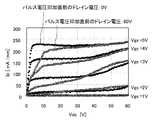
図2は、第1の比較例の窒化物半導体トランジスタにおけるパルス電圧印加時のドレイン電圧(Vds)とドレイン電流(Id)との関係を示す図である。なお、ゲート電極108とドレイン電極107に印加されるパルス電圧のパルス幅は0.5μ秒、パルス間隔は1m秒である。図2に示すように、パルス電圧印加前のバイアス条件としてゲート電圧が0V且つドレイン電圧が60Vの場合は、ゲート電圧が0V且つドレイン電圧が0Vの場合と比較して、パルス電圧印加後に低いドレイン電圧に対するドレイン電流が減少し、オン抵抗が増大している。これが電流コラプスと呼ばれる現象である。電流コラプス現象は、オン抵抗を大幅に増大させるため、高いドレイン電圧が印加されるパワートランジスタにとっては重大な問題となる。 FIG. 2 is a diagram showing the relationship between the drain voltage (Vds) and the drain current (Id) when a pulse voltage is applied in the nitride semiconductor transistor of the first comparative example. Note that the pulse width of the pulse voltage applied to the
この電流コラプス現象のメカニズムを図3および図4を用いて詳細に説明する。図3は、第1の比較例のトランジスタのオフ時における空乏層の拡がりを示す断面図である。また、図4は、第1の比較例のトランジスタにおけるドレイン電圧印加時の空乏層の拡がりを示す断面図である。 The mechanism of this current collapse phenomenon will be described in detail with reference to FIGS. FIG. 3 is a cross-sectional view showing the expansion of the depletion layer when the transistor of the first comparative example is off. FIG. 4 is a cross-sectional view showing the expansion of the depletion layer when the drain voltage is applied in the transistor of the first comparative example.
図3に示すように、第1の比較例のトランジスタではp型GaN層105が設けられているため、チャネルを形成するアンドープAlGaN層104とアンドープGaN層103のヘテロ接合部でのキャリア濃度が小さくなり、ゲート電極108の下方における閾値電圧(チャネルが形成されるために必要とされる印加電圧)Vth1は、例えば+0.5Vと正電圧側に大きくすることができる。ここで、トランジスタをオフ状態とした場合(例えば、ゲート電圧としては0Vの状態か負電圧を印加する状態)、空乏層端305がヘテロ接合部を横切るので、第1の比較例のトランジスタはノーマリーオフ型を実現している。一方、ゲート電極108の側方においては、p型GaN層105が設けられていないため、アンドープAlGaN層104とアンドープGaN層103のヘテロ接合部でのキャリア濃度が大きくなり、この部分の閾値電圧Vth2は、例えば−1Vと負電圧側に小さい値となっている。As shown in FIG. 3, since the p-
上述の第1の比較例のトランジスタにおいて、例えば60V程度の高いドレイン電圧を印加してオフ状態(ゲート電極を0V)とすると、図4に示すように、高いドレイン電圧の印加によってゲート電極108の側方に形成される空乏層(オフ時の空乏層端406)は、図3に示す空乏層(空乏層端305参照)よりもさらに拡がると予想される。なお、ゲート電極108の側方に形成されるオフ時の空乏層端406とオン時の空乏層端407は、同じ位置にある。 In the transistor of the first comparative example described above, when a high drain voltage of about 60 V, for example, is applied to turn it off (the gate electrode is 0 V), as shown in FIG. The depletion layer formed on the side (
上述のオフ状態からドレイン電圧を60V印加したまま例えばゲート電圧を正電圧側(3V)に変化させた直後の空乏層は、表面準位に捕獲された電子405の影響を受け、オフ時の空乏層端406からオン時の空乏層端407のように変化すると推測される。すなわち、表面準位に捕獲された電子405の放出時間が遅いため、ゲート電極108の下方ではチャネルが拡がるが、ゲート電極108の側方ではチャネルが拡がらずにドレイン電流を大きくできないという現象が生じてしまう。これが電流コラプス現象のメカニズムと考えられる。 For example, the depletion layer immediately after changing the gate voltage to the positive voltage side (3 V) while applying the drain voltage of 60 V from the above-described OFF state is affected by the
続いて、上述の電流コラプス現象を解決するために本願発明者らは図5に示す本発明の第2の比較例のトランジスタを考案した。図5は、本発明の第2の比較例のトランジスタの構成を示す断面図である。同図に示すように、第2の比較例のトランジスタの特徴は、アンドープAlGaN層104とp型GaN層105との間にp型AlGaN層505が設けられていることにある。ゲート電極108の下方においては、第1の比較例のトランジスタと同様にして、p型GaN層105が設けられているため、閾値電圧Vth1は、例えば+0.5Vと正電圧側に大きくすることができ、第2の比較例のトランジスタはノーマリーオフ型を実現している。一方、ゲート電極108の側方においても、p型AlGaN層505が設けられていることにより、この部分の閾値電圧Vth2は、例えば−2Vと第1の比較例のトランジスタに比べて小さくすることができる。すなわち、Vth1とVth2の差である閾値電圧差(ΔVth=Vth1−Vth2)は2.5Vとなり、第1の比較例におけるΔVth(1.5V)よりも大きくなる。Subsequently, in order to solve the above-described current collapse phenomenon, the inventors of the present application devised a second comparative example transistor of the present invention shown in FIG. FIG. 5 is a cross-sectional view showing the configuration of the transistor of the second comparative example of the present invention. As shown in the figure, the transistor of the second comparative example is characterized in that a p-
図6は、本発明の第2の比較例のトランジスタにおけるドレイン電圧印加時の空乏層の拡がりを示す断面図である。第2の比較例のトランジスタにおいて、例えば60V程度の高いドレイン電圧を印加してオフ状態とすると、図6に示すように、上述の閾値電圧差ΔVthを大きくとっており、ゲート電極108の側方ではチャネルが開く位置までしか空乏層(オフ時の空乏層端607)が拡がらない。この状態からドレイン電圧を印加したままゲートに正電圧(3V)を印加してオン状態とした場合、ゲート電極108の側方に形成される空乏層(オン時の空乏層端608)は、表面準位に捕獲された電子の影響を受けるためオフ時から変化することなくチャネルが開く位置まで拡がった状態である。ここで、ドレイン電流の状態はゲート電極108の下方に形成される空乏層の位置で決まることより、第2の比較例のトランジスタでは高電圧を印加した後も十分なドレイン電流を観察することができる。従って、第2の比較例のトランジスタを用いれば、電流コラプス現象を抑制することができる。このように電流コラプス現象を抑制するためには、ゲート電極108の側方における閾値電圧が十分負電圧側になるように小さくすることが重要であると考えられる。FIG. 6 is a cross-sectional view showing the expansion of the depletion layer when the drain voltage is applied in the transistor of the second comparative example of the present invention. In the transistor of the second comparative example, when a high drain voltage of about 60 V, for example, is applied and turned off, the above threshold voltage difference ΔVth is large as shown in FIG. On the other hand, the depletion layer (
続いて、第2の比較例のトランジスタにおけるp型AlGaN層505とアンドープAlGaN層104との膜厚を変化させることで、上述の閾値電圧差(ΔVth)について検討した。図7は、閾値電圧差(ΔVth)とパルス電圧印加時のドレイン電流比を示す図である。ここで、測定されたドレイン電流比は、パルス電圧印加時のドレイン電圧が10V、ゲート電圧が5Vの場合のドレイン電流の値について、パルス電圧印加直前のドレイン電圧が0Vである場合と60Vである場合の値の比率を表している。従って、この比率が1に近いほど電流コラプス現象が抑制されており、逆に0に近いほど電流コラプスが大きいことを示す。図7に示すように、ΔVthとドレイン電流比には明確な相関関係があり、ΔVthが大きいほど電流コラプス現象が抑制されることが分かる。特に、ΔVthが2.5V以上であれば、ドレイン電流比はほぼ1となり、完全に電流コラプスが抑制された。Subsequently, the above-described threshold voltage difference (ΔVth ) was examined by changing the film thicknesses of the p-
図8は、第2の比較例のトランジスタにおけるパルス電圧印加時のドレイン電圧(Vds)とドレイン電流(Id)との関係を示す図である。図8に示すように、第2の比較例のトランジスタでは、パルス電圧を印加する直前に高いドレイン電圧(60V)を印加した場合においても、パルス電圧を印加する直前にドレイン電圧が0Vの場合とほぼと同じ特性を示しており、電流コラプス現象が抑制されていることが分かる。 FIG. 8 is a diagram showing the relationship between the drain voltage (Vds) and the drain current (Id) when a pulse voltage is applied in the transistor of the second comparative example. As shown in FIG. 8, in the transistor of the second comparative example, even when a high drain voltage (60 V) is applied immediately before the pulse voltage is applied, the drain voltage is 0 V immediately before the pulse voltage is applied. It shows almost the same characteristics, and it can be seen that the current collapse phenomenon is suppressed.
しかしながら、第2の比較例のトランジスタの構造では、図9に示すような不具合が生じてしまう。図9は、第1の比較例および第2の比較例のトランジスタにおけるリーク電流の値を示す図である。同図に示すように、第2の比較例のトランジスタでは、オフ時にソース電極とドレイン電極との間を流れるリーク電流が第1の比較例のトランジスタに比べて多くなってしまう。これは第2の比較例のトランジスタに新たに設けられたp型AlGaN層を介してリークパスが形成されてしまったためだと考えられる。 However, the structure of the transistor of the second comparative example has a problem as shown in FIG. FIG. 9 is a diagram showing the value of the leakage current in the transistors of the first comparative example and the second comparative example. As shown in the figure, in the transistor of the second comparative example, the leakage current flowing between the source electrode and the drain electrode when off is larger than that of the transistor of the first comparative example. This is presumably because a leak path was formed through the p-type AlGaN layer newly provided in the transistor of the second comparative example.
以上の電流コラプス現象のメカニズムを基に検討を重ねた結果、本願発明者らは以下のトランジスタとその製造方法を用いることで、上述の不具合が解消できることを見出した。 As a result of repeated studies based on the mechanism of the current collapse phenomenon described above, the present inventors have found that the above-described problems can be solved by using the following transistors and their manufacturing methods.
本発明のトランジスタは、基板と、前記基板の上方に形成された第1の半導体層と、前記第1の半導体層上に設けられ、ヘテロ接合により前記第1の半導体層との界面にチャネルを形成し、第1の領域と第2の領域とを有する第2の半導体層と、前記第2の半導体層における前記第1の領域と前記第2の領域とを除く領域の上に形成された第1のp型半導体層と、前記第1のp型半導体層上に形成された第2のp型半導体層と、前記第2のp型半導体層上に形成されたゲート電極と、前記第1の半導体層の上または上方であって、平面的に見て前記ゲート電極の両側方に形成されたソース電極およびドレイン電極とを備えており、前記第1の領域は、平面的に見て前記ゲート電極と前記ドレイン電極の間に設けられ、前記第2の領域は、平面的に見て前記ゲート電極と前記ソース電極の間に設けられている。 The transistor of the present invention includes a substrate, a first semiconductor layer formed over the substrate, and a first semiconductor layer provided on the first semiconductor layer. A channel is formed at the interface between the first semiconductor layer and the heterojunction. Forming a second semiconductor layer having a first region and a second region, and formed on a region of the second semiconductor layer excluding the first region and the second region; A first p-type semiconductor layer; a second p-type semiconductor layer formed on the first p-type semiconductor layer; a gate electrode formed on the second p-type semiconductor layer; A source electrode and a drain electrode formed on both sides of the gate electrode as viewed in a plan view above or above one semiconductor layer, and the first region is viewed in a plan view. The second region is provided between the gate electrode and the drain electrode, and the second region is a plane Look is provided between the source electrode and the gate electrode.
この構成によれば、第2の半導体層と第2のp型半導体層との間に第1のp型半導体層が形成されており、且つ、第1のp型半導体層がドレイン電極およびソース電極と接しないように、第1の領域および第2の領域を隔てて設けられている。これにより、上述の第2の比較例のトランジスタと同様にして、第1のp型半導体層が設けられていることで、ゲート電極の下方における閾値電圧Vth1とゲート電極の側方における閾値電圧Vth2との差を大きくできるため、表面準位の影響を受けにくくなっている。その結果、電流コラプス現象を抑制することができる。さらに、第1のp型半導体層はゲート電極およびドレイン電極と接しないように設けられているため、上述の第2の比較例のトランジスタに比べてリーク電流を低減させることができる。従って、本発明のトランジスタでは、電流コラプス現象が抑制され、且つ、リーク電流が低減されたノーマリーオフ型のトランジスタを実現することができる。According to this configuration, the first p-type semiconductor layer is formed between the second semiconductor layer and the second p-type semiconductor layer, and the first p-type semiconductor layer includes the drain electrode and the source. The first region and the second region are separated from each other so as not to contact the electrode. Thus, similarly to the transistor of the second comparative example described above, the threshold voltage Vth1 below the gate electrode and the threshold voltage on the side of the gate electrode are provided by providing the first p-type semiconductor layer. Since the difference fromVth2 can be increased, the surface level is hardly affected. As a result, the current collapse phenomenon can be suppressed. Furthermore, since the first p-type semiconductor layer is provided so as not to be in contact with the gate electrode and the drain electrode, the leakage current can be reduced as compared with the transistor of the second comparative example. Therefore, in the transistor of the present invention, a normally-off transistor in which the current collapse phenomenon is suppressed and the leakage current is reduced can be realized.
なお、前記第1のp型半導体層はAlxGa1−xN(0≦x≦1)から構成され、前記第2のp型半導体層はAlyGa1−yN(0≦y≦1)から構成されていてもよい。この場合、第1のp型半導体層および第2のp型半導体層の格子定数が、チャネル構造を形成するために設けられた第1の半導体層および第2の半導体層の格子定数と近くなるため、第1の半導体層および第2の半導体層の上方に、結晶欠陥の発生を抑制しつつ第1のp型半導体層および第2のp型半導体層を形成することができる。The first p-type semiconductor layer is made of Alx Ga1-x N (0 ≦ x ≦ 1), and the second p-type semiconductor layer is Aly Ga1-y N (0 ≦ y ≦ 1). 1). In this case, the lattice constants of the first p-type semiconductor layer and the second p-type semiconductor layer are close to the lattice constants of the first semiconductor layer and the second semiconductor layer provided for forming the channel structure. Therefore, the first p-type semiconductor layer and the second p-type semiconductor layer can be formed above the first semiconductor layer and the second semiconductor layer while suppressing generation of crystal defects.
また、前記第1のp型半導体層はAlxGa1−xN(0≦x≦1)から構成され、前記第2のp型半導体層はAlyGa1−yN(0≦y≦1)から構成されており、x≧yであることが望ましい。この場合、上述と同様に第1のp型半導体層の格子定数が第1の半導体層および第2の半導体層の格子定数と近くなるため、結晶欠陥の抑制を抑制しつつ第1のp型半導体層を成長させることができる。さらに、第2のp型半導体層のAl濃度が第1のp型半導体層よりも小さいため、ゲート電極の下方における閾値電圧Vth1をより大きくすることができ、ノーマリーオフ型のトランジスタの実現に有効となる。The first p-type semiconductor layer is made of Alx Ga1-x N (0 ≦ x ≦ 1), and the second p-type semiconductor layer is Aly Ga1-y N (0 ≦ y ≦ 1). 1), and preferably x ≧ y. In this case, since the lattice constant of the first p-type semiconductor layer is close to the lattice constant of the first semiconductor layer and the second semiconductor layer as described above, the first p-type is suppressed while suppressing crystal defects. A semiconductor layer can be grown. Further, since the Al concentration of the second p-type semiconductor layer is lower than that of the first p-type semiconductor layer, the threshold voltage Vth1 below the gate electrode can be increased, and anormally- off transistor can be realized. Effective.
なお、前記第1の領域のゲート長方向の幅は、0.7μm以上4.5μm以下であると、リーク電流の低減と電流コラプス現象の抑制をより効果的に行うことができるため好ましい。 Note that it is preferable that the width of the first region in the gate length direction be 0.7 μm or more and 4.5 μm or less because leakage current can be reduced and current collapse phenomenon can be more effectively suppressed.
次に、本発明のトランジスタの製造方法は、基板の上方に第1の半導体層、第1の領域と第2の領域とを有する第2の半導体層、第1のp型半導体層、およびゲート電極形成領域を有する第2のp型半導体層を順にエピタキシャル成長させる工程(a)と、前記第2のp型半導体層を前記ゲート電極形成領域を残して選択的に除去する工程(b)と、平面的に見て前記第1の領域と前記第2の領域との間に位置する領域上に形成された前記第1のp型半導体層を残して、前記第1のp型半導体層を選択的に除去する工程(c)と、前記工程(c)の後、前記第1の半導体層の上部および前記第2の半導体層を選択的に除去して、平面的に見て前記第1の領域の側方および前記第2の領域の側方に、前記第1の半導体層を露出させるリセスをそれぞれ設ける工程(d)と、前記リセスに金属を埋め込むことにより、前記第2の領域の側方にソース電極を形成し、前記第1の領域の側方にドレイン電極を形成する工程(e)と、前記第2のp型半導体層上にゲート電極を形成する工程(f)とを備えている。 Next, a method for manufacturing a transistor according to the present invention includes a first semiconductor layer, a second semiconductor layer having a first region and a second region above a substrate, a first p-type semiconductor layer, and a gate. A step (a) of sequentially epitaxially growing a second p-type semiconductor layer having an electrode formation region, a step (b) of selectively removing the second p-type semiconductor layer leaving the gate electrode formation region; The first p-type semiconductor layer is selected, leaving the first p-type semiconductor layer formed on a region located between the first region and the second region in plan view. After the step (c) and the step (c), the upper part of the first semiconductor layer and the second semiconductor layer are selectively removed, and the first semiconductor layer is viewed in plan view. A recess that exposes the first semiconductor layer is formed on a side of the region and a side of the second region. A step (d) of providing each, and a step of forming a source electrode on the side of the second region and embedding a metal in the recess, and forming a drain electrode on the side of the first region (e) And a step (f) of forming a gate electrode on the second p-type semiconductor layer.
この方法の特徴は、工程(c)で第1のp型半導体層を所定の領域(平面的に見て第1の領域と第2の領域との間)が残るように除去した後、工程(d)で第1の領域および第2の領域の側方に、ソース電極およびドレイン電極を設けるためのリセスをそれぞれ形成したことにある。これにより、ドレイン電極と第1のp型半導体層との間およびソース電極と第1のp型半導体層との間には、それぞれ第1の領域および第2の領域を底面とする溝が形成されることになる。その結果、第2の半導体層上に、表面準位の影響を抑えることができる第1のp型半導体層を備えることができ、且つ、ソース電極およびドレイン電極と第1のp型半導体層とをそれぞれ電気的に分離することができる。従って、本発明のトランジスタの製造方法を用いると、電流コラプス現象が抑制され、且つ、リーク電流が低減されたノーマリーオフ型のトランジスタを作製することが可能となる。 The feature of this method is that after the first p-type semiconductor layer is removed in step (c) so that a predetermined region (between the first region and the second region in plan view) remains, In (d), recesses for providing the source electrode and the drain electrode are respectively formed on the sides of the first region and the second region. As a result, grooves having the first region and the second region as bottom surfaces are formed between the drain electrode and the first p-type semiconductor layer and between the source electrode and the first p-type semiconductor layer, respectively. Will be. As a result, the first p-type semiconductor layer capable of suppressing the influence of the surface state can be provided on the second semiconductor layer, and the source and drain electrodes, the first p-type semiconductor layer, Can be electrically separated from each other. Therefore, by using the method for manufacturing a transistor of the present invention, it is possible to manufacture a normally-off transistor in which a current collapse phenomenon is suppressed and leakage current is reduced.
本発明のトランジスタおよびその製造方法によれば、第1のp型半導体層を所定の位置に設けることで、リーク電流の低減と電流コラプス現象の抑制が可能なノーマリーオフ型のトランジスタを実現することができる。 According to the transistor and the manufacturing method thereof of the present invention, a normally-off transistor capable of reducing leakage current and suppressing current collapse is realized by providing the first p-type semiconductor layer at a predetermined position. be able to.
(実施形態)
以下、本発明の実施形態に係るJFET構造を有する窒化物半導体トランジスタ(第1のトランジスタ)とその製造方法について図面を参照しながら説明する。図10は、本実施形態の第1のトランジスタの構成を示す断面図である。(Embodiment)
Hereinafter, a nitride semiconductor transistor (first transistor) having a JFET structure according to an embodiment of the present invention and a manufacturing method thereof will be described with reference to the drawings. FIG. 10 is a cross-sectional view showing the configuration of the first transistor of this embodiment.
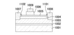
図10に示すように、本実施形態の第1のトランジスタは、サファイアからなり、(0001)面を主面とする基板1001と、基板1001の主面上に形成され、厚さが100nmのAlNなどからなるバッファ層1002と、バッファ層1002上に形成され、厚さが2μmのアンドープのGaNなどからなる第1の半導体層1003と、第1の半導体層1003上に形成され、厚さが25nmのアンドープのAlGaNなどからなる第2の半導体層1004と、第2の半導体層1004の一部上に形成され、厚さが15nmのAlGaNなどからなる第1のp型半導体層1005と、第1のp型半導体層1005上に設けられ、厚さが100nmのGaNなどからなる第2のp型半導体層1006とを備えている。なお、第2の半導体層1004および第1のp型半導体層1005は、例えばAl0.15Ga0.85Nからそれぞれ構成されている。As shown in FIG. 10, the first transistor of this embodiment is made of sapphire, has a
さらに、本実施形態の第1のトランジスタは、第2のp型半導体層1006上にオーミック接合により形成され、Pdなどからなるゲート電極1009と、第2の半導体層1004を貫通して第1の半導体層1003の上部に接し、平面的に見てゲート電極1009の両側方に形成され、例えばTiとAlとからなるソース電極1007およびドレイン電極1008とを備えている。なお、第1のp型半導体層1005は、例えばAlGaN層に濃度が1×1019cm−3程度のMgがドーピングされ、キャリア濃度は1×1018cm−3程度となっている。また、第2のp型半導体層1006は、大部分が第1のp型半導体層1005と同程度のキャリア濃度になっているが、上面からの距離が10nm程度以内の領域では、Mgが1×1020cm−3程度ドーピングされている。なお、第1の半導体層1003と第2の半導体層1004との界面ではヘテロ結合によりチャネルが形成される。また、本実施形態のトランジスタにおいて、ソース電極1007およびドレイン電極1008は、第1の半導体層1003の上部と第2の半導体層1004に埋め込まれて形成されているが、これに限定されるものではなく、第1の半導体層1003の上または上方に設けられていてもよい。Furthermore, the first transistor of this embodiment is formed on the second p-
なお、ここでは、第2の半導体層1004のうちドレイン電極1008の近傍において第1のp型半導体層1005が形成されていない領域を第1の領域とし、ソース電極1007の近傍において第1のp型半導体層1005が形成されていない領域を第2の領域とする。 Note that here, a region where the first p-
また、本実施形態の第1のトランジスタは、第2の比較例のトランジスタと同様にして、GaN層などからなる第2のp型半導体層1006が設けられているため、ゲート電極1009の下方における閾値電圧Vth1を正電圧側に大きくすることができ、第1のトランジスタはノーマリーオフ型を実現している。Further, the first transistor of this embodiment is provided with the second p-
本実施形態のトランジスタの特徴は、第2の半導体層1004と第2のp型半導体層1006との間に第1のp型半導体層1005が設けられており、且つ、第1のp型半導体層1005がドレイン電極1008およびソース電極1007と接しないように、第1の溝1101(第1の領域を底面とする溝)および第2の溝1102(第2の領域を底面とする溝)を隔てて設けられていることにある。この構成では、上述の第2の比較例のトランジスタと同様にして、第1のp型半導体層1005が設けられていることで、ゲート電極1009の下方における閾値電圧Vth1とゲート電極1009の側方における閾値電圧Vth2との差(閾値電圧差ΔVth)を大きくできるため、表面準位の影響を受けにくくなっている。その結果、電流コラプス現象を抑制することができる。さらに、第1のp型半導体層1005は、ゲート電極1009およびドレイン電極1008と溝を隔てて形成されているため、上述の第2の比較例のトランジスタに比べてリーク電流を低減させることができる。従って、本実施形態の第1のトランジスタでは、電流コラプス現象が抑制され、且つ、リーク電流が低減されたノーマリーオフ型のトランジスタを実現することが可能となる。The transistor of this embodiment is characterized in that the first p-
ここで、図11は、第1のトランジスタにおけるパルス電圧印加時のドレイン電圧(Vds)とドレイン電流(Id)との関係を示す図である。同図に示すように、第1のトランジスタでは、上述の第1の比較例のトランジスタの特性(図2参照)と比較して、パルス電圧を印加する直前に高いドレイン電圧(60V)を印加した場合においても、ドレイン電圧が0Vにおいて測定した場合に近い電流値を示しており、電流コラプス現象が抑制されていることが分かる。 Here, FIG. 11 is a diagram showing the relationship between the drain voltage (Vds) and the drain current (Id) when the pulse voltage is applied in the first transistor. As shown in the figure, in the first transistor, compared with the characteristics of the transistor of the first comparative example (see FIG. 2), a higher drain voltage (60 V) was applied immediately before the pulse voltage was applied. Even in this case, the current value is close to that measured when the drain voltage is 0 V, and it can be seen that the current collapse phenomenon is suppressed.
なお、第1のトランジスタでは、第2のp型半導体層1006およびゲート電極1009は、それぞれソース電極1007側に偏って設けられている。これにより、ゲート電極1009とドレイン電極1008との距離が大きくなるため、高いドレイン電圧が印加された際に生じる電界が緩和され、トランジスタの破壊耐圧を向上させることができる。 Note that in the first transistor, the second p-
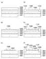
次に、本実施形態に係る第1のトランジスタの製造方法について、図12(a)〜(f)を用いて説明する。図12(a)〜(f)は、第1のトランジスタの製造方法を示す断面図である。 Next, a method for manufacturing the first transistor according to the present embodiment will be described with reference to FIGS. 12A to 12F are cross-sectional views illustrating a method for manufacturing the first transistor.
最初に、図12(a)に示すように、サファイアなどからなる基板1001上に、厚さが100nmでAlNなどからなるバッファ層1002、厚さが2μmでアンドープのGaNなどからなる第1の半導体層1003、厚さが25nmでアンドープのAlGaNなどからなる第2の半導体層1004、厚さが15nmのAlGaNなどからなる第1のp型半導体層1005、および厚さが100nmのGaNなどからなる第2のp型半導体層1006を順にMOCVD(Metal Organic Chemical Vapor Deposition)法によりエピタキシャル成長させる。 First, as shown in FIG. 12A, on a
次に、図12(b)に示すように、第2のp型半導体層1006をドライエッチングにより、後の工程でゲート電極を形成する領域(以下、「ゲート電極形成領域」と称する)を残して、選択的に除去する。続いて、図12(c)に示すように、所定の領域を残して、第1のp型半導体層1005をドライエッチングにより選択的に除去する。ここで、第1のp型半導体層1005は、平面的に見て第2の半導体層1004の第1の領域と第2の領域との間に位置する領域上に形成される。 Next, as shown in FIG. 12B, the second p-
次に、図12(d)に示すように、第1の半導体層1003の上部および第2の半導体層1004を選択的にエッチング除去して、平面的に見て第1のp型半導体層1005の両側方に第1の半導体層1003を露出させるリセスをそれぞれ形成する。 Next, as shown in FIG. 12D, the upper portion of the
続いて、図12(e)に示すように、前の工程で作製したリセスに例えばTiおよびAlを埋め込むことで、ソース電極1007およびドレイン電極1008をそれぞれ形成する。この時、第1のp型半導体層1005は、第1の領域を底面とする第1の溝1101によりドレイン電極1008と隔てられ、第2の領域を底面とする第2の溝1102によりソース電極1007と隔てられている。 Subsequently, as shown in FIG. 12E, a
最後に、図12(f)に示すように、第2のp型半導体層1006のゲート電極形成領域上に、Pdなどからなるゲート電極1009を形成する。以降、所定の工程を経て、本実施形態の第1のトランジスタを作製することができる。 Finally, as shown in FIG. 12F, a
本実施形態の第1のトランジスタの製造方法の特徴は、図12(c)に示す工程で第1のp型半導体層1005を所定の領域(平面的に見て第1の領域と第2の領域との間)に残るように形成した後、図12(d)に示す工程で第1の領域および第2の領域の側方に、ソース電極1007およびドレイン電極1008を設けるためのリセスをそれぞれ形成したことにある。これにより、ドレイン電極1008と第1のp型半導体層1005との間およびソース電極1007と第1のp型半導体層1005との間には、それぞれ第1の溝1101および第2の溝1102が形成されることになる。その結果、第2の半導体層1004上に、表面準位の影響を抑えることができる第1のp型半導体層1005を備えることができ、且つ、ソース電極1007およびドレイン電極1008と第1のp型半導体層1005とをそれぞれ電気的に分離することができる。従って、本実施形態の第1のトランジスタの製造方法を用いると、電流コラプス現象が抑制され、且つ、リーク電流が低減されたノーマリーオフ型のトランジスタを作製することが可能となる。 A feature of the first transistor manufacturing method of this embodiment is that the first p-
なお、ドレイン電極1008と第1のp型半導体層1005との間に設けられた第1の溝1101(第1の領域)のゲート長方向の幅は、0.7μm以上4.5μm以下であることが好ましい。図13は、第1の溝1101の幅に対するドレイン電流比およびリーク電流の値を示した図である。ここで、測定したドレイン電流比は、パルス電圧印加時のドレイン電圧が10V、ゲート電圧が5Vの場合のドレイン電流において、パルス電圧を印加する直前の電圧が0V時に対する60V時の比を表しており、ドレイン電流比が1に近いほど電流コラプス現象が抑制されていることを示している。また、ソース電極とドレイン電極との間のリーク電流は、ドレイン電圧が20V、ゲート電圧が−2Vである場合のオフ時のドレイン電流を示している。なお、第1のトランジスタにおいて、ゲート電極1009とドレイン電極1008との距離は7.5μmである。図13に示すように、ドレイン電流比は第1の溝の幅が広くなるにつれて緩やかに減少している。第1の溝の幅が0.7μmである場合のドレイン電流比は0.8程度となっており、十分に電流コラプスが抑制されていることが分かる。一方、リーク電流は第1の溝の幅が0μmである場合、すなわち第1のp型半導体層1005とドレイン電極1008とが接触している場合のみ大きな値を示している。そして、第1の溝の幅が0.7μm以上であれば1×10−8[A/mm]以下の値を示しており、リーク電流は大幅に低減されている。以上のことより、本実施形態の第1のトランジスタでは、第1の領域の幅を0.7μm以上4.5μm以下とすることで、リーク電流の低減と電流コラプスの抑制とをより効果的に実現することが可能となる。なお、第1の溝の幅は上述の範囲に限定されるものではなく、0.7μm未満であっても、ソース電極1007およびドレイン電極1008と第1のp型半導体層1005とがそれぞれ接触していなければ、リーク電流の低減と電流コラプスの抑制を図ることができる。Note that the width in the gate length direction of the first trench 1101 (first region) provided between the
続いて、本実施形態の第1のトランジスタの変形例として、図14に示す第2のトランジスタについて説明する。図14は、本実施形態に係る第2のトランジスタの構成を示す断面図である。第2のトランジスタでは、第1のp型半導体層1205の構成のみが第1のトランジスタと異なっているため、同様な構成部分については省略する。 Next, a second transistor shown in FIG. 14 will be described as a modification of the first transistor of this embodiment. FIG. 14 is a cross-sectional view showing the configuration of the second transistor according to this embodiment. In the second transistor, only the configuration of the first p-
図14に示すように、本実施形態の第2のトランジスタでは、第1のp型半導体層1205が第1の領域を底面とする第3の溝1201と第2の領域を底面とする第4の溝1202とを有している。そして、第1のp型半導体層1205は、第3の溝1201および第4の溝1202により、ソース電極1007に接する第1の部分と、ゲート電極1009の下方に設けられた第2の部分と、ドレイン電極1008に接する第3の部分とに分断されている。 As shown in FIG. 14, in the second transistor of this embodiment, the first p-
以上の構成によれば、第1のp型半導体層1205とソース電極1007およびドレイン電極1008とは電気的にそれぞれ分離されているため、第2のトランジスタにおいても上述の第1のトランジスタと同様に、リーク電流を低減させつつ、電流コラプス現象を抑制させることができる。 According to the above structure, since the first p-
なお、第2のトランジスタは、上述の第1のトランジスタの製造工程(図12参照)の一部を変更することで作製することができる。具体的には、図12(c)に示す工程で第1のp型半導体層1205をエッチングする際に、平面的に見て第2のp型半導体層1006の両側方に第1の領域を露出させる第3の溝1201および第2の領域を露出させる第4の溝1202をそれぞれ形成する。その後、図12(d)に示す工程で、第1の半導体層1003の上面、第2の半導体層1004、および第3の溝1201および第4の溝1202の側方に位置する第1のp型半導体層1005を選択的に除去する。これらの工程を経て、第1のトランジスタと同様にして第2のトランジスタを製造することができる。 Note that the second transistor can be manufactured by changing part of the manufacturing process of the first transistor (see FIG. 12). Specifically, when the first p-
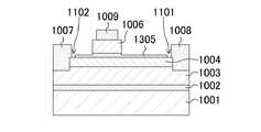
次に、本実施形態の第1のトランジスタの変形例として、図15に示す第3のトランジスタについて説明する。図15は、本実施形態に係る第3のトランジスタの構成を示す断面図である。第3のトランジスタでは、第1のp型半導体層1305の構成のみが第1のトランジスタと異なっているため、同様な構成部分については省略する。 Next, as a modification of the first transistor of this embodiment, a third transistor illustrated in FIG. 15 will be described. FIG. 15 is a cross-sectional view showing the configuration of the third transistor according to this embodiment. In the third transistor, only the configuration of the first p-
図15に示すように、本実施形態の第3のトランジスタでは、第1のp型半導体層1305が凸形状で設けられており、第2のp型半導体層1006と接する部分の膜厚が他の部の膜厚よりも大きくなっている。なお、第2のp型半導体層1006と接する部分の膜厚は例えば20nmであり、平面的に見て第2のp型半導体層1006の側方に形成された部分の膜厚は例えば15nmとなっている。このような構成においても、上述の第1のトランジスタと同様な効果を得ることができる。 As shown in FIG. 15, in the third transistor of this embodiment, the first p-
なお、第3のトランジスタは、上述の第1のトランジスタの製造工程(図12参照)の一部を変更することで作製することができる。具体的には、図12(b)に示す工程で第2のp型半導体層1006を選択的に除去した後、該第2のp型半導体層1006をマスクとして第1のp型半導体層1005をドライエッチングにより例えば5nm分除去する。その後、平面的に見て第1の領域と第2の領域との間に形成された第1のp型半導体層1005が残るように、第1の領域および第2の領域の側方に形成された第1のp型半導体層1005を選択的に除去する。これらの工程を経て、第1のp型半導体層1005を凸形状に形成することができる。 Note that the third transistor can be manufactured by changing part of the manufacturing process of the first transistor described above (see FIG. 12). Specifically, after the second p-
最後に、本実施形態の第1のトランジスタの変形例として、図16に示す第4のトランジスタについて説明する。図16は、本実施形態に係る第4のトランジスタの構成を示す断面図である。第4のトランジスタでは、第2のp型半導体層1406の構成のみが第1のトランジスタと異なっているため、同様な構成部分については省略する。 Finally, a fourth transistor shown in FIG. 16 will be described as a modification of the first transistor of this embodiment. FIG. 16 is a cross-sectional view showing the configuration of the fourth transistor according to this embodiment. In the fourth transistor, only the configuration of the second p-
図16に示すように、本実施形態の第4のトランジスタでは、第1のp型半導体層1005上に第2のp型半導体層1406が凸形状で設けられており、第2のp型半導体層1406のうちゲート電極1009下方に形成された部分の膜厚が他の部分の膜厚よりも大きくなっている。このような構成を有する第4のトランジスタにおいても、第1のトランジスタと同様にリーク電流を低減させることができ、且つ、電流コラプス現象を抑制することが可能となる。なお、平面的に見てゲート電極1009の側方に形成された第2のp型半導体層1406の膜厚が大きくなると、上述の閾値電圧差ΔVthを大きくできないため、この部分の膜厚は20μm以下であることが好ましい。As shown in FIG. 16, in the fourth transistor of this embodiment, the second p-
また、第4のトランジスタは、上述の第1のトランジスタの製造工程(図12参照)の一部を変更することで作製することができる。具体的には、図12(a)に示す工程で第1のp型半導体層1005上に第2のp型半導体層1406を例えば100nm形成した後、図12(b)に示す工程で、ゲート電極形成領域に設けられた第2のp型半導体層1406を残して、ゲート電極形成領域を除く部分に設けられた第2のp型半導体層を例えば80nm分選択的に除去する。その後、図12(c)に示す工程で、平面的に見て第1の領域および第2の領域との間に形成された第1のp型半導体層1005および第2のp型半導体層1406を残して、第1のp型半導体層1005および第2のp型半導体層1406をそれぞれ選択的に除去する。これらの工程を経て、第1のp型半導体層1005上に第2のp型半導体層1406を凸形状に形成することができる。 The fourth transistor can be manufactured by changing part of the manufacturing process of the first transistor described above (see FIG. 12). Specifically, after the second p-
なお、本実施形態のトランジスタ(第1のトランジスタ、第2のトランジスタ、第3のトランジスタ、および第4のトランジスタ)では、第1のp型半導体層はAlxGa1−xN(0≦x≦1)から構成され、第2のp型半導体層はAlyGa1−yN(0≦y≦1)から構成されており、x=yであってもよい。この場合、第1のp型半導体層と第2のp型半導体層が同じ材料から構成され、チャネル構造を形成するために設けられた第1の半導体層および第2の半導体層と格子定数が近くなるため、第1の半導体層および第2の半導体層の上方に、結晶欠陥の発生を抑制しつつ第1のp型半導体層および第2のp型半導体層をエピタキシャル成長させることができる。In the transistor of the present embodiment (the first transistor, the second transistor, the third transistor, and the fourth transistor), the first p-type semiconductor layer is made of Alx Ga1-x N (0 ≦ x ≦ 1), the second p-type semiconductor layer is made of Aly Ga1-y N (0 ≦ y ≦ 1), and x = y may be satisfied. In this case, the first p-type semiconductor layer and the second p-type semiconductor layer are made of the same material, and the lattice constants of the first semiconductor layer and the second semiconductor layer provided to form the channel structure are Therefore, the first p-type semiconductor layer and the second p-type semiconductor layer can be epitaxially grown above the first semiconductor layer and the second semiconductor layer while suppressing generation of crystal defects.
また、第1のp型半導体層はAlxGa1−xN(0≦x≦1)から構成され、第2のp型半導体層はAlyGa1−yN(0≦y≦1)から構成されており、x>yであってもよい。この場合、第1のp型半導体層の格子定数がチャネル構造を形成するための第1の半導体層および第2の半導体層の格子定数と近くなるため、結晶欠陥の発生を抑制しつつ第1のp型半導体層を成長させることができる。さらに、第2のp型半導体層のAl濃度が第1のp型半導体層よりも小さいため、ゲート電極の下方における閾値電圧Vth1をより大きくすることができ、ノーマリーオフ型のトランジスタの実現に有効である。The first p-type semiconductor layer is made of Alx Ga1-x N (0 ≦ x ≦ 1), and the second p-type semiconductor layer is Aly Ga1-y N (0 ≦ y ≦ 1). X> y may be sufficient. In this case, since the lattice constant of the first p-type semiconductor layer is close to the lattice constants of the first semiconductor layer and the second semiconductor layer for forming the channel structure, the first defect is generated while suppressing the generation of crystal defects. The p-type semiconductor layer can be grown. Further, since the Al concentration of the second p-type semiconductor layer is smaller than that of the first p-type semiconductor layer, the
なお、本実施形態のトランジスタにおいて、第1の半導体層と第2の半導体層の界面で形成されるヘテロ接合は、AlzGa1−zN(0<z≦1)とGaNとから構成される接合であれば好ましい。この場合、AlzGa1−zN(0<z≦1)とGaNとのヘテロ接合により、自発分極あるいはピエゾ分極によってヘテロ界面に高濃度のキャリアを発生させることができ、動作時に大きな電流を流すことが可能となる。In the transistor of this embodiment, the heterojunction formed at the interface between the first semiconductor layer and the second semiconductor layer is composed of Alz Ga1-z N (0 <z ≦ 1) and GaN. Bonding is preferable. In this case, the heterojunction of Alz Ga1-z N (0 <z ≦ 1) and GaN can generate high-concentration carriers at the heterointerface due to spontaneous polarization or piezo-polarization, resulting in a large current during operation. It is possible to flow.
なお、上述の実施形態に係るトランジスタにおいて、第2の半導体層1104にそれぞれ設けられた第1の溝1101の底面および第2の溝1102の底面は、オーバーエッチング等により、第2の半導体層1004の他の部分の上面よりも下方に形成されていてもよい。このようなトランジスタにおいても、上述と同様な効果が得られる。 Note that, in the transistor according to the above embodiment, the bottom surface of the
本発明のトランジスタおよびその製造方法は、汎用インバータ等の民生機器の電源回路等で用いられるパワートランジスタなどに有用である。 The transistor of the present invention and the manufacturing method thereof are useful for a power transistor used in a power circuit of a consumer device such as a general-purpose inverter.
101 サファイア基板
102 バッファ層
103 アンドープGaN層
104 アンドープAlGaN層
105 p型GaN層
106 ソース電極
107 ドレイン電極
108 ゲート電極
305 空乏層端
405 電子
406、607 オフ時の空乏層端
407、608 オン時の空乏層端
505 p型AlGaN層
1001 基板
1002 バッファ層
1003 第1の半導体層
1004 第2の半導体層
1005、1205、1305 第1のp型半導体層
1006、1406 第2のp型半導体層
1007 ソース電極
1008 ドレイン電極
1009 ゲート電極
1101 第1の溝
1102 第2の溝
1201 第3の溝
1202 第4の溝101 Sapphire substrate
102 Buffer layer
103 Undoped GaN layer
104 Undoped AlGaN layer
105 p-type GaN layer
106 Source electrode
107 Drain electrode
108 Gate electrode
305 Depletion layer edge
405 electrons
406,607 Depletion layer edge when off
407, 608 ON depletion layer edge
505 p-type AlGaN layer
1001 Substrate
1002 Buffer layer
1003 First semiconductor layer
1004 Second semiconductor layer
1005, 1205, 1305 First p-type semiconductor layer
1006, 1406 Second p-type semiconductor layer
1007 Source electrode
1008 Drain electrode
1009 Gate electrode
1101 First groove
1102 Second groove
1201 3rd groove
1202 4th groove
Claims (19)
Translated fromJapanese前記基板上に形成された第1の半導体層と、
前記第1の半導体層上に設けられ、ヘテロ接合により前記第1の半導体層との界面にチャネルを形成する第2の半導体層と、
前記第2の半導体層上に形成された第1のp型半導体層と、
前記第1のp型半導体層上に形成された第2のp型半導体層と、
前記第2のp型半導体層上に形成されたゲート電極と、
前記第1の半導体層上であって、前記ゲート電極の両側方に形成されたソース電極およびドレイン電極とを備えており、
前記第1のp型半導体層のゲート長に沿った幅は、前記第2のp型半導体層のゲート長に沿った幅よりも大きく、
前記第1のp型半導体層は前記ドレイン電極に接しないように第1の溝を隔てて設けられ、且つ、前記ソース電極と接しないように第2の溝を隔てて設けられ、
前記ゲート電極に電圧を印加することにより、前記第1の半導体層と前記第2の半導体層との界面に正孔が注入され、
前記第1の半導体層、前記第2の半導体層、前記第1のp型半導体層および前記第2のp型半導体層が窒化物半導体により構成されているトランジスタ。A substrate,
A first semiconductor layer formed on the substrate;
A second semiconductor layer provided on the first semiconductor layer and forminga channel at the interface with the first semiconductor layer by a heterojunction;
A first p-type semiconductor layer formedon the second semiconductor layer;
A second p-type semiconductor layer formed on the first p-type semiconductor layer;
A gate electrode formed on the second p-type semiconductor layer;
A first semiconductorlayer, and a source electrode and a drain electrode formed on both sides of thefront Symbol gate electrode,
The width along the gate length of the first p-type semiconductor layer is larger than the width along the gate length of the second p-type semiconductor layer,
The first p-type semiconductor layer is provided with a first groove so as not to contact the drain electrode, and is provided with a second groove so as not to contact the source electrode,
By applying a voltage to the gate electrode, holes are injected into the interface between the first semiconductor layer and the second semiconductor layer,
A transistor in which the first semiconductor layer, the second semiconductor layer, the first p-type semiconductor layer, and the second p-type semiconductor layer are made of a nitride semiconductor .
前記基板上に形成された第1の半導体層と、
前記第1の半導体層上に設けられ、ヘテロ接合により前記第1の半導体層との界面にチャネルを形成する第2の半導体層と、
前記第2の半導体層上に形成された第1のp型半導体層と、
前記第1のp型半導体層上に形成された第2のp型半導体層と、
前記第2のp型半導体層上に形成されたゲート電極と、
前記第1の半導体層上であって、前記ゲート電極の両側方に形成されたソース電極およびドレイン電極とを備えており、
前記第1のp型半導体層のゲート長に沿った幅は、前記第2のp型半導体層のゲート長に沿った幅よりも大きく、
前記第1のp型半導体層は、第3の溝と第4の溝とを有しており、
前記第1のp型半導体層は、前記第3の溝により、前記ソース電極に接する第1の部分と、前記ゲート電極の下方領域を含む第2の部分とに分断され、前記第4の溝により、前記第2の部分と、前記ドレイン電極に接する第3の部分とに分断され、
前記ゲート電極に電圧を印加することにより、前記第1の半導体層と前記第2の半導体層との界面に正孔が注入され、
前記第1の半導体層、前記第2の半導体層、前記第1のp型半導体層および前記第2のp型半導体層が窒化物半導体により構成されているトランジスタ。A substrate,
A first semiconductor layer formed on the substrate;
A second semiconductor layer provided on the first semiconductor layer and forming a channel at the interface with the first semiconductor layer by a heterojunction;
A first p-type semiconductor layer formed on the second semiconductor layer;
A second p-type semiconductor layer formed on the first p-type semiconductor layer;
A gate electrode formed on the second p-type semiconductor layer;
A source electrode and a drain electrode formed on both sides of the gate electrode on the first semiconductor layer;
The width along the gate length of the first p-type semiconductor layer is larger than the width along the gate length of the second p-type semiconductor layer,
The first p-type semiconductor layer hasa third grooveand a fourth groove,
The first p-type semiconductor layer is divided by the third groove into a first part in contact with the source electrode and a second part including a lower region of the gate electrode, and the fourth groove Is divided into the second part and the third part in contact with the drain electrode,
By applying a voltage to the gate electrode, holes are injected into the interface between the first semiconductor layer and the second semiconductor layer,
A transistor in which the first semiconductor layer, the second semiconductor layer, the first p-type semiconductor layer, and the second p-type semiconductor layer are made of a nitride semiconductor.
前記第2のp型半導体層と前記ソース電極との距離は、前記第2のp型半導体層と前記ドレイン電極との距離よりも小さい請求項1〜11のうちいずれか1つに記載のトランジスタ。The distance between the gate electrode and the source electrode is smaller than the distance between the gate electrode and the drain electrode,
The distance between the second p-type semiconductor layer and the source electrode, the transistor according to any one of the second p-type semiconductor layer and the smaller claim than the distance between the drain electrode1-11 .
前記第2のp型半導体層を前記ゲート電極形成領域を残して選択的に除去する工程(b)と、
前記第1の領域と前記第2の領域との間に位置する領域上に形成された前記第1のp型半導体層を残して、前記第1のp型半導体層を選択的に除去する工程(c)と、
前記工程(c)の後、前記第1の半導体層の上部および前記第2の半導体層を選択的に除去して、前記第1の領域の側方および前記第2の領域の側方に、前記第1のp型半導体層から離間して、前記第1の半導体層を露出させるリセスをそれぞれ設ける工程(d)と、
前記リセスに金属を埋め込むことにより、前記第2の領域の側方に前記第1のp型半導体層から離間してソース電極を形成し、前記第1の領域の側方に前記第1のp型半導体層から離間してドレイン電極を形成する工程(e)と、
前記第2のp型半導体層上にゲート電極を形成する工程(f)とを備え、
前記工程(f)で形成される前記ゲート電極に、電圧が印加されることにより前記第2の半導体層の前記第1の半導体層との界面に正孔が注入され、
前記第1の半導体層、前記第2の半導体層、前記第1のp型半導体層および前記第2のp型半導体層が窒化物半導体により構成されていることを特徴とするトランジスタの製造方法。A first semiconductor layeron the substrate, a second semiconductor layer having a first region and a second region, the first p-type semiconductor layer, and a second p-type semiconductor layer having a gate electrode formation region A step (a) of epitaxial growth in sequence;
A step (b) of selectively removing the second p-type semiconductor layer leaving the gate electrode formation region;
Leaving the first p-type semiconductor layer formed on a region located between thefront Symbol first region and the second region, selectively removing the first p-type semiconductor layer Step (c);
After the step (c), selectively removing the top and the second semiconductor layer of the first semiconductorlayer, before SL side of the lateral and the second region of the first region And (d) providing a recessapart from the first p-type semiconductor layer to expose the first semiconductor layer,
By embedding the metal in said recess, saidspaced apart from the first p-type semiconductor layer forming a source electrode on the side of the second region,said first p laterally of said first region Forming a drain electrodespaced apart from the type semiconductor layer ; and
Forming a gate electrode on the second p-type semiconductor layer (f),
When a voltage is applied to the gate electrode formed in the step (f), holes are injected into the interface between the second semiconductor layer and the first semiconductor layer,
A method for manufacturinga transistor, wherein the first semiconductor layer, the second semiconductor layer, the first p-type semiconductor layer, and the second p-type semiconductor layer are made of a nitride semiconductor .
前記第2のp型半導体層を前記ゲート電極形成領域を残して選択的に除去する工程(b)と、A step (b) of selectively removing the second p-type semiconductor layer leaving the gate electrode formation region;
前記第3の領域と前記第4の領域との間に位置する領域上に形成された前記第1のp型半導体層を残して、前記第1のp型半導体層を選択的に除去する工程(c)と、A step of selectively removing the first p-type semiconductor layer, leaving the first p-type semiconductor layer formed on a region located between the third region and the fourth region; (C),
前記工程(c)の後、前記第1の半導体層の上部および前記第2の半導体層を選択的に除去して、前記第3の領域の側方および前記第4の領域の側方に、前記第1の半導体層を露出させるリセスをそれぞれ設ける工程(d)と、After the step (c), the upper portion of the first semiconductor layer and the second semiconductor layer are selectively removed, to the side of the third region and the side of the fourth region, Providing a recess for exposing the first semiconductor layer, respectively (d);
前記リセスに金属を埋め込むことにより、前記第3の領域の側方にソース電極を形成し、前記第4の領域の側方にドレイン電極を形成する工程(e)と、Forming a source electrode laterally of the third region by embedding a metal in the recess and forming a drain electrode laterally of the fourth region;
前記第2のp型半導体層上にゲート電極を形成する工程(f)とを備え、Forming a gate electrode on the second p-type semiconductor layer (f),
前記工程(c)では、前記ソース電極と前記第3の領域との間に位置する領域上に形成された、前記第1のp型半導体層の第1の部分と、前記第3の領域と前記第4の領域との間に位置する領域上に形成された、前記第1のp型半導体層の第2の部分と、前記第4の領域と前記ドレイン電極との間に位置する領域上に形成された、前記第1のp型半導体層の第3の部分とを各々分断して形成し、In the step (c), a first portion of the first p-type semiconductor layer formed on a region located between the source electrode and the third region, the third region, The second portion of the first p-type semiconductor layer formed on the region located between the fourth region and the region located between the fourth region and the drain electrode Formed by dividing each of the third portions of the first p-type semiconductor layer,
前記工程(f)で形成される前記ゲート電極に、電圧が印加されることにより前記第2の半導体層の前記第1の半導体層との界面に正孔が注入され、When a voltage is applied to the gate electrode formed in the step (f), holes are injected into the interface between the second semiconductor layer and the first semiconductor layer,
前記第1の半導体層、前記第2の半導体層、前記第1のp型半導体層および前記第2のp型半導体層が窒化物半導体により構成されていることを特徴とするトランジスタの製造方法。A method for manufacturing a transistor, wherein the first semiconductor layer, the second semiconductor layer, the first p-type semiconductor layer, and the second p-type semiconductor layer are made of a nitride semiconductor.
前記工程(c)では、前記第1の領域と前記第2の領域との間に位置する領域上に形成された前記第1のp型半導体層および前記第2のp型半導体層を残して、前記第1のp型半導体層および前記第2のp型半導体層を選択的に除去する請求項15に記載のトランジスタの製造方法。In the step (b), the second p-type semiconductor layer is selectively removed so that the film thickness in the gate electrode formation region is a convex shape larger than the film thickness of other parts,
In the step(c), leaving the first p-type semiconductor layer and the second p-type semiconductor layer formed on a region located between thefront Symbol first region and the second region The method of manufacturing a transistor according to claim 15, wherein the first p-type semiconductor layer and the second p-type semiconductor layer are selectively removed.
前記第1のp型半導体層を凸型に形成する請求項15に記載のトランジスタの製造方法。In the step (b), after the second p-type semiconductor layer is selectively removed leaving the gate electrode formation region, a part of the exposed portion of the first p-type semiconductor layer is removed. In addition,
The method of manufacturing a transistor according to claim 15, wherein the first p-type semiconductor layer is formed in a convex shape.
Priority Applications (2)
| Application Number | Priority Date | Filing Date | Title |
|---|---|---|---|
| JP2006344323AJP4712683B2 (en) | 2006-12-21 | 2006-12-21 | Transistor and manufacturing method thereof |
| US11/939,899US7663161B2 (en) | 2006-12-21 | 2007-11-14 | Transistor for preventing current collapse and having improved leakage current characteristics and method for fabricating the same |
Applications Claiming Priority (1)
| Application Number | Priority Date | Filing Date | Title |
|---|---|---|---|
| JP2006344323AJP4712683B2 (en) | 2006-12-21 | 2006-12-21 | Transistor and manufacturing method thereof |
Publications (3)
| Publication Number | Publication Date |
|---|---|
| JP2008159681A JP2008159681A (en) | 2008-07-10 |
| JP2008159681A5 JP2008159681A5 (en) | 2009-09-17 |
| JP4712683B2true JP4712683B2 (en) | 2011-06-29 |
Family
ID=39541558
Family Applications (1)
| Application Number | Title | Priority Date | Filing Date |
|---|---|---|---|
| JP2006344323AActiveJP4712683B2 (en) | 2006-12-21 | 2006-12-21 | Transistor and manufacturing method thereof |
Country Status (2)
| Country | Link |
|---|---|
| US (1) | US7663161B2 (en) |
| JP (1) | JP4712683B2 (en) |
Families Citing this family (33)
| Publication number | Priority date | Publication date | Assignee | Title |
|---|---|---|---|---|
| JP2009164235A (en)* | 2007-12-28 | 2009-07-23 | Rohm Co Ltd | Nitride semiconductor device and manufacturing method thereof |
| CN102388441B (en) | 2009-04-08 | 2014-05-07 | 宜普电源转换公司 | Enhanced GaN high electron mobility transistor device and fabrication method thereof |
| US9818857B2 (en) | 2009-08-04 | 2017-11-14 | Gan Systems Inc. | Fault tolerant design for large area nitride semiconductor devices |
| US9029866B2 (en) | 2009-08-04 | 2015-05-12 | Gan Systems Inc. | Gallium nitride power devices using island topography |
| JP5618571B2 (en)* | 2010-03-02 | 2014-11-05 | パナソニック株式会社 | Field effect transistor |
| EP2559064A4 (en)* | 2010-04-13 | 2018-07-18 | GaN Systems Inc. | High density gallium nitride devices using island topology |
| JP5605134B2 (en)* | 2010-09-30 | 2014-10-15 | 富士通セミコンダクター株式会社 | Semiconductor device and manufacturing method thereof |
| US9214538B2 (en) | 2011-05-16 | 2015-12-15 | Eta Semiconductor Inc. | High performance multigate transistor |
| JP2013074068A (en)* | 2011-09-27 | 2013-04-22 | Fujitsu Ltd | Semiconductor device and manufacturing method of semiconductor device |
| JP2013074070A (en)* | 2011-09-27 | 2013-04-22 | Fujitsu Ltd | Semiconductor device and manufacturing method of semiconductor device |
| US8785944B2 (en)* | 2011-12-07 | 2014-07-22 | Samsung Electronics Co., Ltd. | High electron mobility transistor |
| KR101934851B1 (en)* | 2011-12-07 | 2019-01-04 | 삼성전자주식회사 | High electron mobility transistor |
| US8669591B2 (en) | 2011-12-27 | 2014-03-11 | Eta Semiconductor Inc. | E-mode HFET device |
| KR101922122B1 (en)* | 2012-09-28 | 2018-11-26 | 삼성전자주식회사 | Normally off high electron mobility transistor |
| KR101922121B1 (en) | 2012-10-09 | 2018-11-26 | 삼성전자주식회사 | High electron mobility transistor and method of manufacturing the same |
| JP6167889B2 (en)* | 2012-12-21 | 2017-07-26 | 日亜化学工業株式会社 | Field effect transistor and manufacturing method thereof |
| TWI497721B (en)* | 2013-05-27 | 2015-08-21 | Univ Nat Chiao Tung | Enhanced gallium nitride crystal and forming method thereof |
| JP2015173151A (en)* | 2014-03-11 | 2015-10-01 | 株式会社東芝 | semiconductor device |
| JP5669119B1 (en)* | 2014-04-18 | 2015-02-12 | 株式会社パウデック | Semiconductor element, electric device, bidirectional field effect transistor, and mounting structure |
| US9871067B2 (en)* | 2015-11-17 | 2018-01-16 | Taiwan Semiconductor Manufacturing Co., Ltd. | Infrared image sensor component |
| KR102402771B1 (en) | 2015-12-11 | 2022-05-26 | 삼성전자주식회사 | Semiconductor device and method for fabricating the same |
| JP6614116B2 (en)* | 2016-05-24 | 2019-12-04 | 株式会社デンソー | Semiconductor device |
| CN105870013A (en)* | 2016-06-08 | 2016-08-17 | 苏州能屋电子科技有限公司 | Method for realizing enhanced HEMT by p-type passivation and enhanced HEMT |
| US9673311B1 (en) | 2016-06-14 | 2017-06-06 | Semiconductor Components Industries, Llc | Electronic device including a multiple channel HEMT |
| TWI613814B (en)* | 2016-11-29 | 2018-02-01 | 新唐科技股份有限公司 | Enhancement mode hemt device |
| JP6834546B2 (en)* | 2017-02-03 | 2021-02-24 | サンケン電気株式会社 | Semiconductor devices and their manufacturing methods |
| JPWO2020031636A1 (en)* | 2018-08-09 | 2021-08-12 | ソニーセミコンダクタソリューションズ株式会社 | Semiconductor devices and methods for manufacturing semiconductor devices |
| JP7513595B2 (en)* | 2019-04-15 | 2024-07-09 | ローム株式会社 | Nitride semiconductor device and method for manufacturing same |
| JP7535258B2 (en)* | 2020-03-31 | 2024-08-16 | 豊田合成株式会社 | Semiconductor elements and devices |
| FR3115156B1 (en) | 2020-10-09 | 2022-08-26 | Commissariat Energie Atomique | Gallium nitride transistor |
| US20220130988A1 (en)* | 2020-10-27 | 2022-04-28 | Texas Instruments Incorporated | Electronic device with enhancement mode gallium nitride transistor, and method of making same |
| CN113972270B (en)* | 2021-09-10 | 2025-07-04 | 华为技术有限公司 | Field effect transistor, preparation method thereof and electronic circuit |
| WO2024024475A1 (en)* | 2022-07-27 | 2024-02-01 | ローム株式会社 | Nitride semiconductor device |
Family Cites Families (25)
| Publication number | Priority date | Publication date | Assignee | Title |
|---|---|---|---|---|
| US5162877A (en)* | 1987-01-27 | 1992-11-10 | Fujitsu Limited | Semiconductor integrated circuit device and method of producing same |
| US5161235A (en)* | 1990-02-20 | 1992-11-03 | University Of Virginia Alumni Patents Foundation | Field-effect compound semiconductive transistor with GaAs gate to increase barrier height and reduce turn-on threshold |
| US5298441A (en)* | 1991-06-03 | 1994-03-29 | Motorola, Inc. | Method of making high transconductance heterostructure field effect transistor |
| JPH11261053A (en)* | 1998-03-09 | 1999-09-24 | Furukawa Electric Co Ltd:The | High mobility transistor |
| JP2000349095A (en)* | 1999-06-04 | 2000-12-15 | Sony Corp | Semiconductor device and its manufacture, power amplifier, and wireless communication device |
| JP2001284576A (en)* | 2000-03-30 | 2001-10-12 | Toshiba Corp | High electron mobility transistor and method of manufacturing the same |
| ATE359602T1 (en)* | 2000-06-02 | 2007-05-15 | Microgan Gmbh | HETEROSTRUCTURE WITH BACK DONATOR DOPPING |
| US6992319B2 (en)* | 2000-07-18 | 2006-01-31 | Epitaxial Technologies | Ultra-linear multi-channel field effect transistor |
| JP3836697B2 (en)* | 2000-12-07 | 2006-10-25 | 日本碍子株式会社 | Semiconductor element |
| JP2004273486A (en) | 2003-03-05 | 2004-09-30 | Mitsubishi Electric Corp | Semiconductor device and method of manufacturing the same |
| US6919590B2 (en)* | 2003-08-29 | 2005-07-19 | Motorola, Inc. | Heterojunction bipolar transistor with monolithically integrated junction field effect transistor and method of manufacturing same |
| US7501669B2 (en)* | 2003-09-09 | 2009-03-10 | Cree, Inc. | Wide bandgap transistor devices with field plates |
| US7382004B2 (en)* | 2003-11-25 | 2008-06-03 | Sensor Electronic Technology, Inc. | Semiconductor sensing device |
| US7382001B2 (en) | 2004-01-23 | 2008-06-03 | International Rectifier Corporation | Enhancement mode III-nitride FET |
| JP4041075B2 (en)* | 2004-02-27 | 2008-01-30 | 株式会社東芝 | Semiconductor device |
| JP2006032911A (en)* | 2004-06-15 | 2006-02-02 | Ngk Insulators Ltd | Semiconductor laminated structure, semiconductor element and HEMT element |
| US7119381B2 (en)* | 2004-07-30 | 2006-10-10 | Freescale Semiconductor, Inc. | Complementary metal-oxide-semiconductor field effect transistor structure having ion implant in only one of the complementary devices |
| JP4705412B2 (en) | 2005-06-06 | 2011-06-22 | パナソニック株式会社 | Field effect transistor and manufacturing method thereof |
| US7364988B2 (en)* | 2005-06-08 | 2008-04-29 | Cree, Inc. | Method of manufacturing gallium nitride based high-electron mobility devices |
| JP4712459B2 (en) | 2005-07-08 | 2011-06-29 | パナソニック株式会社 | Transistor and method of operating the same |
| EP1978550A4 (en)* | 2005-12-28 | 2009-07-22 | Nec Corp | FIELD EFFECT TRANSISTOR, AND MULTILAYER EPITAXIAL FILM FOR USE IN FIELD EFFECT TRANSISTOR PREPARATION |
| US7728355B2 (en)* | 2005-12-30 | 2010-06-01 | International Rectifier Corporation | Nitrogen polar III-nitride heterojunction JFET |
| WO2007116517A1 (en)* | 2006-04-10 | 2007-10-18 | Fujitsu Limited | Compound semiconductor structure and process for producing the same |
| US7504679B2 (en)* | 2006-07-20 | 2009-03-17 | International Rectifier Corporation | Enhancement mode GaN FET with piezoelectric gate |
| JP4755961B2 (en) | 2006-09-29 | 2011-08-24 | パナソニック株式会社 | Nitride semiconductor device and manufacturing method thereof |
- 2006
- 2006-12-21JPJP2006344323Apatent/JP4712683B2/enactiveActive
- 2007
- 2007-11-14USUS11/939,899patent/US7663161B2/enactiveActive
Also Published As
| Publication number | Publication date |
|---|---|
| JP2008159681A (en) | 2008-07-10 |
| US7663161B2 (en) | 2010-02-16 |
| US20080149965A1 (en) | 2008-06-26 |
Similar Documents
| Publication | Publication Date | Title |
|---|---|---|
| JP4712683B2 (en) | Transistor and manufacturing method thereof | |
| JP5032965B2 (en) | Nitride semiconductor transistor and manufacturing method thereof | |
| JP5468768B2 (en) | Field effect transistor and manufacturing method thereof | |
| JP4755961B2 (en) | Nitride semiconductor device and manufacturing method thereof | |
| JP4712459B2 (en) | Transistor and method of operating the same | |
| US10026834B2 (en) | Method of manufacturing enhanced device and enhanced device | |
| JP5084262B2 (en) | Semiconductor device | |
| US8390029B2 (en) | Semiconductor device for reducing and/or preventing current collapse | |
| CN102292801B (en) | Field effect transistor and method of manufacturing the same | |
| JP5342152B2 (en) | Gallium nitride epitaxial crystal and method for producing the same | |
| JP5190923B2 (en) | Nitride semiconductor transistor having GaN as channel layer and manufacturing method thereof | |
| KR101092467B1 (en) | Enhancement normally off nitride semiconductor device and manufacturing method thereof | |
| JP2008153330A (en) | Nitride semiconductor high electron mobility transistor | |
| WO2009110254A1 (en) | Field effect transistor and method for manufacturing the same | |
| TW201436008A (en) | Heterojunction transistor and method of manufacturing same | |
| JP2006222160A (en) | Field effect transistor and its manufacturing method | |
| JP2008306083A (en) | Iii-v nitride semiconductor field-effect transistor and its manufacturing method | |
| WO2020158394A1 (en) | Nitride semiconductor device | |
| JP4815020B2 (en) | Nitride semiconductor device | |
| JP5721782B2 (en) | Semiconductor device | |
| JP2011142358A (en) | Nitride semiconductor device | |
| JP5470786B2 (en) | Semiconductor device | |
| JP2007103778A (en) | Field effect transistor | |
| WO2022201841A1 (en) | Nitride semiconductor device | |
| CN116072723A (en) | Apparatus and method for controlling threshold voltage and gate leakage current of a GaN-based semiconductor device |
Legal Events
| Date | Code | Title | Description |
|---|---|---|---|
| A521 | Request for written amendment filed | Free format text:JAPANESE INTERMEDIATE CODE: A523 Effective date:20090731 | |
| A621 | Written request for application examination | Free format text:JAPANESE INTERMEDIATE CODE: A621 Effective date:20090731 | |
| A131 | Notification of reasons for refusal | Free format text:JAPANESE INTERMEDIATE CODE: A131 Effective date:20101116 | |
| A521 | Request for written amendment filed | Free format text:JAPANESE INTERMEDIATE CODE: A523 Effective date:20110106 | |
| TRDD | Decision of grant or rejection written | ||
| A01 | Written decision to grant a patent or to grant a registration (utility model) | Free format text:JAPANESE INTERMEDIATE CODE: A01 Effective date:20110222 | |
| A61 | First payment of annual fees (during grant procedure) | Free format text:JAPANESE INTERMEDIATE CODE: A61 Effective date:20110323 | |
| R150 | Certificate of patent or registration of utility model | Ref document number:4712683 Country of ref document:JP Free format text:JAPANESE INTERMEDIATE CODE: R150 | |
| S533 | Written request for registration of change of name | Free format text:JAPANESE INTERMEDIATE CODE: R313533 | |
| R350 | Written notification of registration of transfer | Free format text:JAPANESE INTERMEDIATE CODE: R350 |