JP4712497B2 - Filter circuit, and image sensor, image sensor module, and image reading apparatus using the same - Google Patents
Filter circuit, and image sensor, image sensor module, and image reading apparatus using the sameDownload PDFInfo
- Publication number
- JP4712497B2 JP4712497B2JP2005268047AJP2005268047AJP4712497B2JP 4712497 B2JP4712497 B2JP 4712497B2JP 2005268047 AJP2005268047 AJP 2005268047AJP 2005268047 AJP2005268047 AJP 2005268047AJP 4712497 B2JP4712497 B2JP 4712497B2
- Authority
- JP
- Japan
- Prior art keywords
- image sensor
- filter circuit
- current
- constant current
- mirror
- Prior art date
- Legal status (The legal status is an assumption and is not a legal conclusion. Google has not performed a legal analysis and makes no representation as to the accuracy of the status listed.)
- Expired - Fee Related
Links
- 239000003990capacitorSubstances0.000claimsdescription34
- 230000005669field effectEffects0.000claimsdescription30
- 238000005070samplingMethods0.000claimsdescription10
- 238000001914filtrationMethods0.000claimsdescription8
- 230000003139buffering effectEffects0.000claimsdescription5
- 238000010586diagramMethods0.000description19
- 238000007599dischargingMethods0.000description8
- 101100508840Daucus carota INV3 geneProteins0.000description6
- 101100524516Saccharomyces cerevisiae (strain ATCC 204508 / S288c) RFA2 geneProteins0.000description6
- 238000000034methodMethods0.000description6
- 230000000630rising effectEffects0.000description6
- 239000000758substrateSubstances0.000description5
- 238000007796conventional methodMethods0.000description4
- 101100033865Saccharomyces cerevisiae (strain ATCC 204508 / S288c) RFA1 geneProteins0.000description3
- 238000003384imaging methodMethods0.000description3
- 230000010354integrationEffects0.000description3
- 230000008569processEffects0.000description3
- 230000003111delayed effectEffects0.000description2
- 230000009191jumpingEffects0.000description2
- 230000002093peripheral effectEffects0.000description2
- 239000004065semiconductorSubstances0.000description2
- 238000007493shaping processMethods0.000description2
- 230000001360synchronised effectEffects0.000description2
- 230000007704transitionEffects0.000description2
- 101150070189CIN3 geneProteins0.000description1
- 101150110971CIN7 geneProteins0.000description1
- 101100286980Daucus carota INV2 geneProteins0.000description1
- 101150110298INV1 geneProteins0.000description1
- 101100397044Xenopus laevis invs-a geneProteins0.000description1
- 101100397045Xenopus laevis invs-b geneProteins0.000description1
- 230000002411adverseEffects0.000description1
- 230000008859changeEffects0.000description1
- 230000000295complement effectEffects0.000description1
- 230000000694effectsEffects0.000description1
- 238000003780insertionMethods0.000description1
- 230000037431insertionEffects0.000description1
- 230000007257malfunctionEffects0.000description1
- 229910044991metal oxideInorganic materials0.000description1
- 150000004706metal oxidesChemical class0.000description1
- 230000009467reductionEffects0.000description1
Images


Classifications
- H—ELECTRICITY
- H04—ELECTRIC COMMUNICATION TECHNIQUE
- H04N—PICTORIAL COMMUNICATION, e.g. TELEVISION
- H04N25/00—Circuitry of solid-state image sensors [SSIS]; Control thereof
- H04N25/60—Noise processing, e.g. detecting, correcting, reducing or removing noise
- H—ELECTRICITY
- H04—ELECTRIC COMMUNICATION TECHNIQUE
- H04N—PICTORIAL COMMUNICATION, e.g. TELEVISION
- H04N25/00—Circuitry of solid-state image sensors [SSIS]; Control thereof
- H04N25/70—SSIS architectures; Circuits associated therewith
- H04N25/76—Addressed sensors, e.g. MOS or CMOS sensors
- H04N25/78—Readout circuits for addressed sensors, e.g. output amplifiers or A/D converters
Landscapes
- Engineering & Computer Science (AREA)
- Multimedia (AREA)
- Signal Processing (AREA)
- Facsimile Heads (AREA)
- Networks Using Active Elements (AREA)
Description
Translated fromJapanese本発明は、フィルタ回路、並びに、これを用いたイメージセンサ、イメージセンサモジュール、画像読取装置に関するものである。 The present invention relates to a filter circuit, and an image sensor, an image sensor module, and an image reading apparatus using the filter circuit.
スキャナやディジタル複合機など、フラットベッド型の画像読取装置を備えたアプリケーションでは、その構造上、セット基板とイメージセンサモジュールとを接続するための信号ライン、並びに、イメージセンサモジュール上でI/O[Input/Output]とイメージセンサICとを接続するための信号ラインが長距離にわたって引き回されることが多い。 In an application including a flatbed type image reading apparatus such as a scanner or a digital multi-function peripheral, a signal line for connecting the set substrate and the image sensor module as well as an I / O [ In many cases, signal lines for connecting [Input / Output] and the image sensor IC are routed over a long distance.
特に、密着型のイメージセンサモジュールは、複数のイメージセンサICを各受光素子の配列方向に縦列して成る構造上、モジュール上における信号ラインの引き回しが非常に長く、信号ラインに飛び込む外来ノイズによって、イメージセンサICのロジック部が誤った動作を行い、読取画像信号に乱れを生じるおそれがあった。 In particular, the contact type image sensor module has a structure in which a plurality of image sensor ICs are arranged in a row in the arrangement direction of the respective light receiving elements, and the signal line routing on the module is very long. Due to external noise jumping into the signal line, There is a possibility that the logic part of the image sensor IC performs an incorrect operation and the read image signal is disturbed.
そのため、従来の画像読取装置では、外来ノイズを除去すべく、信号ラインにRCフィルタ回路を挿入する構成が一般に採用されていた。 Therefore, a conventional image reading apparatus generally employs a configuration in which an RC filter circuit is inserted into a signal line in order to remove external noise.
なお、本願発明に関連するその他の従来技術としては、充放電用コンデンサと、前記コンデンサに接続されて出力電圧を出力するRCフィルタと、入力電圧が前記コンデンサの端子電圧より高いときに前記コンデンサを充電する充電回路と、入力電圧が前記コンデンサの端子電圧より低いときに前記コンデンサを放電する放電回路と、を設けたことを特徴とするフィルタ回路が開示・提案されている(特許文献1を参照)。 Other conventional techniques related to the present invention include a charging / discharging capacitor, an RC filter connected to the capacitor and outputting an output voltage, and the capacitor when the input voltage is higher than the terminal voltage of the capacitor. A filter circuit comprising a charging circuit for charging and a discharging circuit for discharging the capacitor when an input voltage is lower than a terminal voltage of the capacitor has been disclosed and proposed (see Patent Document 1) ).
また、本願発明に関連するその他の従来技術としては、入力信号を複数回サンプリングし、そのサンプリング結果を多数決するディジタルフィルタ回路が種々開示・提案されている(例えば、特許文献2〜5を参照)。 As other conventional techniques related to the present invention, various digital filter circuits that sample an input signal a plurality of times and determine the majority of the sampling results have been disclosed and proposed (see, for example,
確かに、信号ラインにRCフィルタ回路を挿入すれば、外来ノイズの悪影響を低減してイメージセンサICの動作精度を高めることができ、延いては、読取画像信号の品質向上を図ることが可能である。 Certainly, if an RC filter circuit is inserted in the signal line, the adverse effect of external noise can be reduced and the operation accuracy of the image sensor IC can be improved, and as a result, the quality of the read image signal can be improved. is there.
しかしながら、RCフィルタ回路の時定数(フィルタ定数)は、回路を構成する抵抗の抵抗値とコンデンサの容量値との積で決まるため、当該RCフィルタ回路をイメージセンサICに集積化する場合には、チップ面積の制約によって、そのフィルタ定数がおのずと制限されていた。そのため、信号ライン毎にフィルタ定数を広範囲に設定しなければならない場合には、RCフィルタ回路をディスクリート部品で構成せざるを得ず、これが装置規模の縮小阻害要因の一つとなっていた。 However, since the time constant (filter constant) of the RC filter circuit is determined by the product of the resistance value of the resistor constituting the circuit and the capacitance value of the capacitor, when integrating the RC filter circuit in the image sensor IC, The filter constant was naturally limited by the restriction of the chip area. For this reason, when the filter constant must be set in a wide range for each signal line, the RC filter circuit has to be configured with discrete components, which is one of the factors that hinder the reduction of the device scale.
なお、特許文献1の従来技術であれば、抵抗値や容量値を変更することなく、フィルタ回路の時定数や入力信号の振幅を制御することが可能である。しかしながら、当該従来技術は、充電回路(カレントミラー回路)の電源電圧ラインと放電回路(カレントミラー回路)の基準電圧ラインにいずれも入力信号を供給し、入力信号の電圧レベルと充放電用コンデンサの端子電圧との高低に応じて、充電回路及び放電回路の動作可否、延いては、前記コンデンサの充電動作/放電動作を切り替える構成とされていた。そのため、入力信号のドライブ能力を十分に高めておかなければ、充電回路や放電回路をドライブすることができず、コンデンサの充放電電流に狂いが生じて、フィルタ定数が所望値から外れてしまうおそれがあった。 In the prior art disclosed in
また、特許文献2〜4の従来技術では、抵抗やコンデンサを要することなく、外来ノイズを除去することが可能ではあるが、当該従来技術では、入力信号のサンプリングクロックに同期したようなパルスノイズ(フリップフロップのセットアップ、ホールドタイム以上のパルス幅を有するノイズ)が連続的に重畳すると、誤動作を生じるおそれがあった。 Further, in the conventional techniques of
本発明は、上記の問題点に鑑み、入力信号のドライブ能力に依ることなく、フィルタ定数を高精度かつ広範囲に設定することができ、かつ、その集積化に際しても装置規模の増大を抑制することが可能なフィルタ回路、並びに、これを用いたイメージセンサ、イメージセンサモジュール、画像読取装置を提供することを目的とする。 In view of the above problems, the present invention can set a filter constant with high accuracy and a wide range without depending on the drive capability of an input signal, and suppresses an increase in the scale of the apparatus even during integration. It is an object of the present invention to provide a filter circuit capable of performing the above, an image sensor, an image sensor module, and an image reading apparatus using the filter circuit.
上記の目的を達成するために、本発明に係るフィルタ回路は、第1定電流を生成する第1定電流源と;第2定電流を生成する第2定電流源と;一対の第1、第2Pチャネル型電界効果トランジスタによって形成され、第1定電流に応じた第1ミラー電流を生成する第1カレントミラー部と;一対の第1、第2Nチャネル型電界効果トランジスタによって形成され、第2定電流に応じた第2ミラー電流を生成する第2カレントミラー部と;入力パルス信号をバッファする入力バッファと;ソースが電源に接続され、ドレインが第1、第2Pチャネル型電界効果トランジスタの両ゲートに接続され、ゲートが前記入力バッファの出力端に接続された第3Pチャネル型電界効果トランジスタと;ソースが接地され、ドレインが第1、第2Nチャネル型電界効果トランジスタの両ゲートに接続され、ゲートが前記入力バッファの出力端に接続された第3Nチャネル型電界効果トランジスタと;第1ミラー電流によって充電され、第2ミラー電流によって放電されるコンデンサと;前記コンデンサの一端電圧を出力パルス信号として出力する出力バッファと;を有して成る構成(第1の構成)としている。 In order to achieve the above object, a filter circuit according to the present invention includes: a first constant current source that generates a first constant current; a second constant current source that generates a second constant current; A first current mirror unit that is formed by a second P-channel field effect transistor and generates a first mirror current corresponding to the first constant current; and a second current channel unit formed by a pair of first and second N-channel field effect transistors, A second current mirror section for generating a second mirror current according to a constant current; an input buffer for buffering an input pulse signal; a source connected to a power supply, and a drain for both the first and second P-channel field effect transistors A third P-channel field effect transistor connected to the gate and having the gate connected to the output terminal of the input buffer; the source is grounded, and the drain is the first and second N-channels A third N-channel field effect transistor connected to both gates of the field effect transistor and having the gate connected to the output terminal of the input buffer; a capacitor charged by the first mirror current and discharged by the second mirror current; An output buffer that outputs one end voltage of the capacitor as an output pulse signal (first configuration).
或いは、本発明に係るフィルタ回路は、上記の電界効果トランジスタに代えてバイポーラトランジスタを用いた構成、すなわち、第1定電流を生成する第1定電流源と;第2定電流を生成する第2定電流源と;一対の第1、第2PNP型バイポーラトランジスタによって形成され、第1定電流に応じた第1ミラー電流を生成する第1カレントミラー部と;一対の第1、第2NPN型バイポーラトランジスタによって形成され、第2定電流に応じた第2ミラー電流を生成する第2カレントミラー部と;入力パルス信号をバッファする入力バッファと;エミッタが電源に接続され、コレクタが第1、第2PNP型バイポーラトランジスタの両ベースに接続され、ベースが前記入力バッファの出力端に接続された第3PNP型バイポーラトランジスタと;エミッタが接地され、コレクタが第1、第2NPN型バイポーラトランジスタの両ベースに接続され、ベースが前記入力バッファの出力端に接続された第3NPN型バイポーラトランジスタと;第1ミラー電流によって充電され、第2ミラー電流によって放電されるコンデンサと;前記コンデンサの一端電圧を出力パルス信号として出力する出力バッファと;を有して成る構成(第2の構成)としてもよい。 Alternatively, the filter circuit according to the present invention has a configuration in which a bipolar transistor is used instead of the field effect transistor, that is, a first constant current source that generates a first constant current; and a second constant that generates a second constant current. A constant current source; a first current mirror section formed by a pair of first and second PNP bipolar transistors and generating a first mirror current corresponding to the first constant current; a pair of first and second NPN bipolar transistors A second current mirror unit configured to generate a second mirror current according to a second constant current; an input buffer for buffering an input pulse signal; an emitter connected to a power supply; and a collector of a first and second PNP type A third PNP-type bipolar transistor is connected to both bases of the bipolar transistor, and the base is connected to the output terminal of the input buffer. A third NPN bipolar transistor having an emitter grounded, a collector connected to both bases of the first and second NPN bipolar transistors, and a base connected to the output terminal of the input buffer; and charged by a first mirror current And a capacitor discharged by the second mirror current; and an output buffer that outputs one end voltage of the capacitor as an output pulse signal (second configuration).
なお、上記第1または第2の構成から成るフィルタ回路は、前記出力パルス信号を複数回サンプリングする手段と、そのサンプリング結果を多数決して出力する手段と、を備えて成る構成(第3の構成)にするとよい。 The filter circuit having the first or second configuration includes a means for sampling the output pulse signal a plurality of times and a means for never outputting a large number of sampling results (third configuration). It is good to.
また、本発明に係るイメージセンサは、受光素子を用いて原稿からの反射光量に応じたアナログの読取画像信号を生成し、これを画素毎にシリアル出力するイメージセンサであって、前記イメージセンサの駆動及び/または制御に必要な入力パルス信号のフィルタ手段として、上記第1〜第3いずれかの構成から成るフィルタ回路を備えて成る構成(第4の構成)としている。 An image sensor according to the present invention is an image sensor that generates an analog read image signal corresponding to the amount of light reflected from a document using a light receiving element, and serially outputs this signal for each pixel. As a filter means for an input pulse signal necessary for driving and / or control, a configuration (fourth configuration) including the filter circuit having any one of the first to third configurations is employed.
また、本発明に係るイメージセンサモジュールは、複数のイメージセンサを各受光素子の配列方向に縦列して成るイメージセンサモジュールであって、前記イメージセンサとして、上記第4の構成から成るイメージセンサを備えた構成(第5の構成)としている。 The image sensor module according to the present invention is an image sensor module formed by cascading a plurality of image sensors in the arrangement direction of the respective light receiving elements, and includes the image sensor having the fourth configuration as the image sensor. Configuration (fifth configuration).
また、本発明に係る画像読取装置は、上記第5の構成から成るイメージセンサモジュールを備えて成る構成(第6の構成)としている。 The image reading apparatus according to the present invention has a configuration (sixth configuration) including the image sensor module having the fifth configuration.
本発明によれば、入力信号のドライブ能力に依ることなく、フィルタ定数を高精度かつ広範囲に設定することができ、かつ、その集積化に際しても装置規模の増大を抑制することが可能なフィルタ回路、並びに、これを用いたイメージセンサ、イメージセンサモジュール、画像読取装置を提供することが可能となる。 According to the present invention, it is possible to set a filter constant with high accuracy and in a wide range without depending on the drive capability of an input signal, and to suppress an increase in the scale of the apparatus even in the integration thereof. It is possible to provide an image sensor, an image sensor module, and an image reading apparatus using the same.
図1は、本発明に係るイメージセンサモジュールを備えた画像読取装置の一実施形態を示す模式図である。 FIG. 1 is a schematic diagram illustrating an embodiment of an image reading apparatus including an image sensor module according to the present invention.
本図に示すように、本実施形態の画像読取装置は、密着型のイメージセンサモジュール1(以下、CIS[Contact Image Sensor]モジュール1と呼ぶ)と、セット基板2と、フレキシブルケーブル3と、を有して成る。また、本図には示していないが、本実施形態の画像読取装置は、上記構成要素のほかにも、原稿を照射する光源や、原稿からの反射光をCISモジュール1に導くレンズアレイなど、画像読取装置の機能を実現するに際して必須の構成要素を当然に有して成る。 As shown in the figure, the image reading apparatus according to the present embodiment includes a contact image sensor module 1 (hereinafter referred to as a CIS [Contact Image Sensor] module 1), a
なお、本発明に係るCISモジュール1の搭載対象となる画像読取装置としては、ファクシミリ、プリンタ、ディジタル複写機、スキャナ、及び、これらの諸機能を備えた複合機(MFP[Multi Function Peripheral])など、シートフィード型やフラットベッド型の画像読取装置を備えたアプリケーション全般を挙げることができる。 The image reading apparatus to which the
CISモジュール1は、n(≧2)個のイメージセンサIC11〜1nを各受光素子の配列方向に縦列して成る。イメージセンサIC11〜1nは、原稿の幅方向に沿って1列(或いはRGBの3列)に配列された受光素子列(CCD[Charge Coupled Devices]型やCMOS[Complementary Metal Oxide Semiconductor]型の固体撮像素子)を用いて原稿からの反射光量に応じたアナログ画像信号を生成し、これを画素毎にシリアル出力する半導体集積回路装置である。なお、CISモジュール1上における信号ラインL1〜L3の配線長は、読取り対象となる原稿の幅に応じて、数十[cm](A4原稿対応機種では約20[cm])とされている。また、イメージセンサIC11〜1nの各受光素子の配列については、その高解像度化を図るべく、千鳥配列としてもよい。 The
セット基板2は、CISモジュール1の制御主体であるCPU[Central Processing Unit]等が搭載された基板である。CPUは、CISモジュール1に対して、イメージセンサIC11〜Inの駆動及び/または制御に必要な入力パルス信号(クロックパルス信号CLK、スタートパルス信号SP、及び、モード切替信号MODE)を伝達する一方、CISモジュール1からのアナログ画像信号をディジタル画像信号に変換して取り込む。 The
フレキシブルケーブル3は、CISモジュール1とセット基板2とを電気的に接続するためのケーブルであり、そのケーブル長は、読取り対象となる原稿の高さ(原稿の走査距離)に応じて、数十[cm](A4原稿対応機種では約50[cm])とされている。なお、本図においては、フレキシブルケーブル3に含まれる信号ラインとして、イメージセンサIC11〜Inの駆動及び/または制御に必要な入力パルス信号(クロックパルス信号CLK、スタートパルス信号SP、及び、モード切替信号MODE)を伝達する信号ラインL1〜L3を代表的に図示したが、信号ラインはこれに限定されるものではなく、フレキシブルケーブル3には、その他にも種々の信号ラインが含まれている。 The
上記構成から成る画像読取装置では、原稿と等幅のCISモジュール1を原稿の高さ方向に走査することで、2次元の画像信号を得ることが可能である。また、CISモジュール1を用いた構成(すなわち、密着方式を採用した構成)であれば、レンズ結像方式を採用した構成と異なり、レンズとセンサとの間に焦点距離を確保する必要がないため、装置の小型化を図ることが可能となる。 In the image reading apparatus configured as described above, a two-dimensional image signal can be obtained by scanning the
なお、先述したように、上記構成から成る画像読取装置では、フレキシブルケーブル3のケーブル長や、CISモジュール1上における信号ラインL1〜L3の配線長が非常に長いため、信号ラインL1〜L3に外来ノイズが飛び込みやすい状況となっている。 As described above, in the image reading apparatus configured as described above, the cable length of the
次に、イメージセンサIC11〜1nの第1実施形態について詳細な説明を行う。 Next, the first embodiment of the image sensor ICs 11 to 1n will be described in detail.
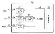
図2は、イメージセンサIC11〜1nの第1実施形態を示すブロック図である。 FIG. 2 is a block diagram showing a first embodiment of the image sensor ICs 11 to 1n.
なお、図2では、特にイメージセンサIC11の第1実施形態(以下、「イメージセンサIC11a」と符号する)を代表として示しているが、その他のイメージセンサIC12〜1nについても、図2と同様の構成から成るものとする。 In FIG. 2, the first embodiment of the image sensor IC 11 (hereinafter referred to as “
図2に示すように、本実施形態のイメージセンサIC11aは、パッドT1〜T3と、アナログフィルタ回路AF1〜AF3と、ロジック部LGと、受光素子列SNと、を有して成る。 As shown in FIG. 2, the
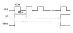
信号ラインL1を用いて伝達されるクロックパルス信号CLKは、イメージセンサIC11〜Inの駆動に必要なクロック信号であり、パッドT1及びアナログフィルタ回路AF1を介して、ロジック部LGに入力される。なお、クロックパルス信号CLKの周波数は、数[MHz](本実施形態では5[MHz])とされており、そのパルス幅は、数百[ns](本実施形態では100[ns])とされている(図3を参照)。 The clock pulse signal CLK transmitted using the signal line L1 is a clock signal necessary for driving the image sensor ICs 11 to In, and is input to the logic unit LG via the pad T1 and the analog filter circuit AF1. The frequency of the clock pulse signal CLK is several [MHz] (5 [MHz] in this embodiment), and the pulse width is several hundred [ns] (100 [ns] in this embodiment). (See FIG. 3).
信号ラインL2を用いて伝達されるスタートパルス信号SPは、原稿の読取開始を指示するための命令信号であり、パッドT2及びアナログフィルタ回路AF2を介して、ロジック部LGに入力される。なお、スタートパルス信号SPは、クロックパルス信号CLKに同期してその論理が変遷される2値信号であり、原稿の読取り開始に際して、クロックパルス信号CLKの1周期分(本実施形態では200[ns])だけ、イネーブル(ハイレベル)とされる(図3を参照)。 The start pulse signal SP transmitted using the signal line L2 is a command signal for instructing the start of reading of the document, and is input to the logic unit LG via the pad T2 and the analog filter circuit AF2. Note that the start pulse signal SP is a binary signal whose logic is changed in synchronization with the clock pulse signal CLK. At the start of reading a document, one cycle of the clock pulse signal CLK (in this embodiment, 200 [ns ]) Is enabled (high level) only (see FIG. 3).
信号ラインL3を用いて伝達されるモード切替信号MODEは、原稿の読取解像度を300dpi[dot per inch]と600dpiのいずれか一に切り替えるための選択信号であり、パッドT3及びアナログフィルタ回路AF3を介して、ロジック部LGに入力される。なお、モード切替信号MODEは、クロックパルス信号CLKに同期してその論理が変遷される2値信号であり、少なくとも原稿の読取り開始から終了までの期間は、一の論理に保持される(図3を参照)。 The mode switching signal MODE transmitted using the signal line L3 is a selection signal for switching the reading resolution of the original to either 300 dpi [dot per inch] or 600 dpi, and passes through the pad T3 and the analog filter circuit AF3. Are input to the logic unit LG. The mode switching signal MODE is a binary signal whose logic is changed in synchronization with the clock pulse signal CLK, and is held at one logic at least during the period from the start to the end of reading of the document (FIG. 3). See).
アナログフィルタ回路AF1〜AF3は、入力パルス信号(CLK、SP、MODE)から信号ラインL1〜L3に飛び込む外来ノイズを各々除去するように波形整形を行い、当該波形整形済みの出力パルス信号S1〜S3をロジック部LGに送出するアナログフィルタ手段である。 The analog filter circuits AF1 to AF3 perform waveform shaping so as to remove external noises jumping from the input pulse signals (CLK, SP, MODE) to the signal lines L1 to L3, respectively, and the waveform-shaped output pulse signals S1 to S3. Is an analog filter means for sending the signal to the logic unit LG.
ロジック部LGは、アナログフィルタ回路AF1〜AF3からの出力パルス信号S1〜S3に基づいて、受光素子列SNを用いたアナログ画像信号の生成、並びに、その画素毎のシリアル出力を制御する。 Based on the output pulse signals S1 to S3 from the analog filter circuits AF1 to AF3, the logic unit LG controls generation of an analog image signal using the light receiving element array SN and serial output for each pixel.
次に、アナログフィルタ回路AF1〜AF3の一構成例について詳細な説明を行う。 Next, one configuration example of the analog filter circuits AF1 to AF3 will be described in detail.
図4は、アナログフィルタ回路AF1〜AF3の一構成例を示す回路図である。 FIG. 4 is a circuit diagram showing a configuration example of the analog filter circuits AF1 to AF3.
なお、図4では、特にアナログフィルタ回路AF1の一構成例を代表として示しているが、その他のアナログフィルタ回路AF2〜AF3についても、図4と同様の構成から成るものとする。 In FIG. 4, one example of the configuration of the analog filter circuit AF1 is shown as a representative. However, the other analog filter circuits AF2 to AF3 have the same configuration as that of FIG.
図4に示す通り、本構成例のアナログフィルタ回路AF1は、一端が接地された第1定電流源I1と;一端が電源に接続された第2定電流源I2と;ソースが電源に接続され、ドレインが第1定電流源I1の他端に接続され、ゲートが自身のドレインに接続された第1Pチャネル型電界効果トランジスタP1と;ソースが電源に接続され、ゲートが第1Pチャネル型電界効果トランジスタP1のゲートに接続された第2Pチャネル型電界効果トランジスタP2と;ソースが接地され、ドレインが第2定電流源I2の他端に接続され、ゲートが自身のドレインに接続された第1Nチャネル型電界効果トランジスタN1と;ソースが接地され、ゲートが第1Nチャネル型電界効果トランジスタN1のゲートに接続された第2Nチャネル型電界効果トランジスタN2と;入力パルス信号(クロックパルス信号CLK)をバッファして出力する入力バッファBUF1と;ソースが電源に接続され、ドレインが第1、第2Pチャネル型電界効果トランジスタP1、P2の両ゲートに接続され、ゲートが入力バッファBUF1の出力端に接続された第3Pチャネル型電界効果トランジスタP3と;ソースが接地され、ドレインが第1、第2Nチャネル型電界効果トランジスタN1、N2の両ゲートに接続され、ゲートが入力バッファBUF1の出力端に接続された第3Nチャネル型電界効果トランジスタN3と;一端が第2Pチャネル型電界効果トランジスタP2のドレイン及び第2Nチャネル型電界効果トランジスタN2のドレインに各々接続され、他端が接地されたコンデンサC1と;コンデンサC1の一端電圧Vcを出力パルス信号S1として出力する出力バッファBUF2と;を有して成る。 As shown in FIG. 4, the analog filter circuit AF1 of this configuration example includes a first constant current source I1 whose one end is grounded; a second constant current source I2 whose one end is connected to a power source; and a source connected to the power source. A first P-channel field effect transistor P1 having a drain connected to the other end of the first constant current source I1 and a gate connected to its own drain; a source connected to a power source and a gate connected to the first P-channel field effect A second P-channel field effect transistor P2 connected to the gate of the transistor P1, a first N-channel having a source grounded, a drain connected to the other end of the second constant current source I2, and a gate connected to its own drain A second N-channel field effect having a source grounded and a gate connected to the gate of the first N-channel field-effect transistor N1 A transistor N2, an input buffer BUF1 for buffering and outputting an input pulse signal (clock pulse signal CLK), a source connected to a power source, and a drain connected to both gates of the first and second P-channel field effect transistors P1 and P2. A third P-channel field effect transistor P3 having a gate connected to the output terminal of the input buffer BUF1, a source grounded, and a drain connected to both gates of the first and second N-channel field effect transistors N1 and N2. A third N-channel field effect transistor N3 having a gate connected to the output terminal of the input buffer BUF1, and one end connected to the drain of the second P-channel field effect transistor P2 and the drain of the second N-channel field effect transistor N2, respectively. And the other end of the capacitor C1 is grounded; An output buffer BUF2 to output an end voltage Vc of capacitors C1 as an output pulse signal S1; comprising a.
第1、第2定電流源I1、I2は、それぞれ、所定の第1、第2定電流i1、i2を生成する手段である。なお、第1、第2定電流源I1、I2として、抵抗素子を要しないバンドギャップ補償定電流源を採用すれば、周囲温度の変化に依らない第1、第2定電流i1、i2を生成することができる。従って、抵抗素子を要するRCフィルタ回路に比べて温度特性の面で有利となる。 The first and second constant current sources I1 and I2 are means for generating predetermined first and second constant currents i1 and i2, respectively. In addition, if the band gap compensation constant current source which does not require a resistance element is adopted as the first and second constant current sources I1 and I2, the first and second constant currents i1 and i2 that do not depend on the change in the ambient temperature are generated. can do. Therefore, it is advantageous in terms of temperature characteristics as compared with an RC filter circuit that requires a resistance element.
一対のトランジスタP1、P2によって形成される第1カレントミラー部CM1は、第1定電流i1に応じた第1ミラー電流m1を生成する手段である。なお、第1定電流i1と第1ミラー電流m1との比は、トランジスタP1、P2のゲート面積比に応じて、適宜調節することが可能である。 The first current mirror unit CM1 formed by the pair of transistors P1 and P2 is a unit that generates the first mirror current m1 corresponding to the first constant current i1. The ratio between the first constant current i1 and the first mirror current m1 can be appropriately adjusted according to the gate area ratio of the transistors P1 and P2.
一対のトランジスタN1、N2によって形成される第2カレントミラー部CM2は、第2定電流i2に応じた第2ミラー電流m2を生成する手段である。なお、第2定電流i2と第2ミラー電流m2との比は、トランジスタN1、N2のゲート面積比に応じて、適宜調節することが可能である。 The second current mirror unit CM2 formed by the pair of transistors N1 and N2 is a unit that generates a second mirror current m2 corresponding to the second constant current i2. The ratio between the second constant current i2 and the second mirror current m2 can be appropriately adjusted according to the gate area ratio of the transistors N1 and N2.
コンデンサC1は、第1ミラー電流m1によって充電され、第2ミラー電流m2によって放電される充放電手段であり、その端子電圧Vcが後段に引き出されている。 The capacitor C1 is charging / discharging means that is charged by the first mirror current m1 and discharged by the second mirror current m2, and the terminal voltage Vc is drawn to the subsequent stage.
入力バッファBUF1は、入力されるクロックパルス信号CLKのドライブ能力を高める手段であり、インバータINV1、INV2を直列接続することで形成されている。 The input buffer BUF1 is means for increasing the drive capability of the input clock pulse signal CLK, and is formed by connecting inverters INV1 and INV2 in series.
出力バッファBUF2は、コンデンサC1の端子電圧Vcを出力パルス信号S1として波形整形するとともに、そのドライブ能力を高める手段であり、インバータINV3、INV4を直列接続することで形成されている。なお、前段のインバータINV3は、2値の閾値電圧(上側閾値電圧VthHと下側閾値電圧VthL)を備えたヒステリシス構成とされている。すなわち、インバータINV3の出力論理は、コンデンサC1の端子電圧Vcが上側閾値電圧VthHを上回ったときに第1論理から第2論理に遷移され、以後、下側閾値電圧VthLを下回ったときに第2論理から第1論理に復帰される。 The output buffer BUF2 is a means for shaping the waveform of the terminal voltage Vc of the capacitor C1 as an output pulse signal S1 and increasing its drive capability, and is formed by connecting inverters INV3 and INV4 in series. The inverter INV3 in the previous stage has a hysteresis configuration having a binary threshold voltage (an upper threshold voltage VthH and a lower threshold voltage VthL). That is, the output logic of the inverter INV3 transitions from the first logic to the second logic when the terminal voltage Vc of the capacitor C1 exceeds the upper threshold voltage VthH, and thereafter, when the terminal voltage Vc falls below the lower threshold voltage VthL. The logic is restored to the first logic.
上記構成から成るアナログフィルタ回路AF1の動作について、図4とともに図5を参照しながら詳細に説明する。 The operation of the analog filter circuit AF1 having the above configuration will be described in detail with reference to FIG. 5 together with FIG.
図5は、アナログフィルタ回路AF1の動作を説明するための図であり、上から順に、クロックパルス信号CLK、コンデンサC1の端子電圧Vc、及び、出力パルス信号S1の波形挙動をそれぞれ示している。 FIG. 5 is a diagram for explaining the operation of the analog filter circuit AF1, and shows the waveform behavior of the clock pulse signal CLK, the terminal voltage Vc of the capacitor C1, and the output pulse signal S1 in order from the top.
まず、正常なクロックパルス信号CLKが入力された場合について説明する。 First, a case where a normal clock pulse signal CLK is input will be described.
この場合、クロックパルス信号CLKがハイレベルに立ち上がると、トランジスタP3がオフとなり、トランジスタN3がオンとなるので、第1カレントミラー部CM1のミラー動作が許可され、第2カレントミラー部CM2のミラー動作が禁止される。その結果、コンデンサC1には、第1ミラー電流m1が流し込まれ、その端子電圧Vcが所定の時定数をもって立ち上がる。その後、コンデンサC1の端子電圧VcがインバータINV3の上側閾値電圧VthHを上回ると、出力パルス信号S1がハイレベルに立ち上がる。 In this case, when the clock pulse signal CLK rises to a high level, the transistor P3 is turned off and the transistor N3 is turned on. Therefore, the mirror operation of the first current mirror unit CM1 is permitted, and the mirror operation of the second current mirror unit CM2 is performed. Is prohibited. As a result, the first mirror current m1 flows into the capacitor C1, and the terminal voltage Vc rises with a predetermined time constant. Thereafter, when the terminal voltage Vc of the capacitor C1 exceeds the upper threshold voltage VthH of the inverter INV3, the output pulse signal S1 rises to a high level.
一方、クロックパルス信号CLKがローレベルに立ち下がると、トランジスタP3がオンとなり、トランジスタN3がオフとなるので、第1カレントミラー部CM1のミラー動作が禁止され、第2カレントミラー部CM2のミラー動作が許可される。その結果、コンデンサC1からは、第2ミラー電流m2が引き抜かれ、その端子電圧Vcが所定の時定数をもって立ち下がる。その後、コンデンサC1の端子電圧VcがインバータINV3の下側閾値電圧VthLを下回ると、出力パルス信号S1がローレベルに立ち下がる。 On the other hand, when the clock pulse signal CLK falls to the low level, the transistor P3 is turned on and the transistor N3 is turned off, so that the mirror operation of the first current mirror unit CM1 is prohibited and the mirror operation of the second current mirror unit CM2 is performed. Is allowed. As a result, the second mirror current m2 is extracted from the capacitor C1, and the terminal voltage Vc falls with a predetermined time constant. Thereafter, when the terminal voltage Vc of the capacitor C1 falls below the lower threshold voltage VthL of the inverter INV3, the output pulse signal S1 falls to a low level.
このように、正常なクロックパルス信号CLKが入力されている場合、アナログフィルタ回路AF1で得られる出力パルス信号S1は、入力されたクロックパルス信号CLKそのものとなる。 Thus, when a normal clock pulse signal CLK is input, the output pulse signal S1 obtained by the analog filter circuit AF1 is the input clock pulse signal CLK itself.
次に、信号ラインL1に外来ノイズが重畳した場合について説明する。 Next, a case where external noise is superimposed on the signal line L1 will be described.
図5に示すように、クロックパルス信号CLKが本来ローレベルである期間に外来ノイズが重畳すると、コンデンサC1は、本来の放電期間中に誤って充電されることになる。しかしながら、外来ノイズの重畳は瞬時的なものであるため、その誤充電は、コンデンサC1の端子電圧VcがインバータINV3の上側閾値電圧VthHに至る前に終了され、再び本来の放電期間に復帰される。従って、出力パルス信号S1は、上記の外来ノイズが除去された波形となる。 As shown in FIG. 5, when external noise is superimposed during a period when the clock pulse signal CLK is originally at a low level, the capacitor C1 is erroneously charged during the original discharge period. However, since the superposition of external noise is instantaneous, the erroneous charging is terminated before the terminal voltage Vc of the capacitor C1 reaches the upper threshold voltage VthH of the inverter INV3, and is restored to the original discharge period again. . Therefore, the output pulse signal S1 has a waveform from which the external noise is removed.
上記構成から成るアナログフィルタ回路AF1であれば、コンデンサC1の充放電電流となる第1、第2ミラー電流m1、m2を適宜調整することにより、そのフィルタ定数を広範囲(例えば、数[ns]〜数十[μs])に設定することができるので、信号ラインL1〜L3毎(入力パルス信号毎)に最適なフィルタ定数を設定することが可能となる。 In the case of the analog filter circuit AF1 having the above-described configuration, the filter constants can be adjusted within a wide range (for example, several [ns] to [n] It is possible to set an optimum filter constant for each of the signal lines L1 to L3 (for each input pulse signal).
本実施形態を例に挙げて、より具体的に述べると、アナログフィルタ回路AF1、AF2のフィルタ定数については、クロックパルス信号CLK及びスタートパルス信号SPのパルス幅がいずれも数百[ns]程度であることに鑑み、第1、第2ミラー電流m1、m2を大きくして、両入力パルス信号に影響を及ぼさない範囲(数十[ns])に設定する一方、アナログフィルタ回路AF3のフィルタ定数については、モード切替信号MODEのパルス幅が上記に比べて非常に長く、フィルタリング処理による影響を受けにくいことに鑑み、外来ノイズの除去効率を優先すべく、第1、第2ミラー電流m1、m2を十分に絞って、数十[μs]に設定することが可能となる。従って、各入力パルス信号につき、そのノイズ耐性を適切にかつ効果的に高めることが可能となる。 More specifically, taking this embodiment as an example, regarding the filter constants of the analog filter circuits AF1 and AF2, the pulse widths of the clock pulse signal CLK and the start pulse signal SP are both about several hundreds [ns]. In view of this, the first and second mirror currents m1 and m2 are increased and set to a range (several tens [ns]) that does not affect both input pulse signals, while the filter constant of the analog filter circuit AF3 is set. In view of the fact that the pulse width of the mode switching signal MODE is much longer than the above and is not easily affected by the filtering process, the first and second mirror currents m1 and m2 are set to give priority to the removal efficiency of external noise. It is possible to set it to several tens [μs] by sufficiently narrowing down. Therefore, it is possible to appropriately and effectively increase the noise tolerance of each input pulse signal.
なお、RCフィルタ回路のフィルタ定数を数十[μs]まで大きくするためには、非常に大きな抵抗値或いは容量値が必要となるため、当該回路の集積化は非現実的となるが、上記構成から成るアナログフィルタ回路AF1であれば、抵抗値或いは容量値を変えずにフィルタ定数を大きくすることができるので、ICへの集積化にも非常に好適である。 Note that in order to increase the filter constant of the RC filter circuit to several tens [μs], a very large resistance value or capacitance value is required. If the analog filter circuit AF1 is composed of the above, it is possible to increase the filter constant without changing the resistance value or the capacitance value, which is very suitable for integration in an IC.
また、上記構成から成るアナログフィルタ回路AF1は、入力パルス信号(クロックパルス信号CLK)に応じてトランジスタP3、N3のオン/オフ制御を行い、トランジスタP1、P2、及び、トランジスタN1、N2のゲート電圧を直接的に制御することで、第1、第2カレントミラー部CM1、CM2の動作可否を制御する構成とされている。すなわち、上記構成から成るアナログフィルタ回路AF1であれば、インピーダンス的にドライブ能力の乏しい入力バッファBUF1を用いた場合でも、トランジスタP3、N3のゲート制御が可能でありさえすれば、第1、第2カレントミラー部CM1、CM2のドライブ不能が生じることはない。従って、コンデンサC1の充放電電流に狂いが生じにくくなり、フィルタ定数が所望値から外れてしまうおそれを低減することが可能となる。 The analog filter circuit AF1 having the above configuration performs on / off control of the transistors P3 and N3 according to the input pulse signal (clock pulse signal CLK), and the gate voltages of the transistors P1 and P2 and the transistors N1 and N2. Is controlled directly to control whether the first and second current mirror units CM1 and CM2 can operate. That is, in the case of the analog filter circuit AF1 having the above configuration, the first and second transistors can be used as long as the gate control of the transistors P3 and N3 can be performed even when the input buffer BUF1 having a poor driving capability is used. Inability to drive the current mirror units CM1 and CM2 does not occur. Therefore, the charge / discharge current of the capacitor C1 is less likely to be distorted, and the risk that the filter constant deviates from a desired value can be reduced.
また、上記構成から成るアナログフィルタ回路AF1であれば、第1、第2ミラー電流m1、m2のバランスを適宜調整することにより、立上がりノイズに対する耐性のみを高めたり、逆に、立下がりノイズに対する耐性のみを高めたりすることが可能となる。 Further, in the case of the analog filter circuit AF1 having the above-described configuration, by appropriately adjusting the balance between the first and second mirror currents m1 and m2, only the resistance against rising noise is increased, or conversely, the resistance against falling noise. It becomes possible to raise only.
例えば、スタートパルス信号SPのように、画像読取りの開始時のみハイレベルに遷移する入力パルス信号をフィルタ対象とする場合には、殆どの期間がローレベルであることに鑑み、第1ミラー電流m1を絞って、立上がりノイズに対する耐性を高めることが考えられる。逆に、上記の論理が逆である入力パルス信号をフィルタ対象とする場合には、殆どの期間がハイレベルであることに鑑み、第2ミラー電流m2を絞って、立下がりノイズに対する耐性を高めればよい。 For example, in the case where an input pulse signal that transitions to a high level only at the start of image reading, such as the start pulse signal SP, is to be filtered, the first mirror current m1 It is conceivable to increase the tolerance against rising noise by narrowing down. On the other hand, when an input pulse signal having the above logic opposite is to be filtered, the second mirror current m2 can be reduced to increase the resistance to falling noise in view of the fact that most periods are at a high level. That's fine.
次に、イメージセンサIC11〜1nの第2実施形態について詳細な説明を行う。 Next, the second embodiment of the image sensor ICs 11 to 1n will be described in detail.
図6は、イメージセンサIC11〜1nの第2実施形態を示すブロック図である。 FIG. 6 is a block diagram showing a second embodiment of the image sensor ICs 11 to 1n.
なお、図6では、特にイメージセンサIC11の第2実施形態(以下、「イメージセンサIC11b」と符号する)を代表として示しているが、その他のイメージセンサIC12〜1nについても、図6と同様の構成から成るものとする。 In FIG. 6, the second embodiment of the image sensor IC 11 (hereinafter referred to as “
図6に示すように、本実施形態のイメージセンサIC11bは、第1実施形態とほぼ同様の構成から成り、アナログフィルタ回路AF2の後段に、ディジタルフィルタ回路DFを設けたことを特徴としている。そこで、第1実施形態と同様の構成部分については、図2と同一符号を付すことで詳細な説明を省略し、以下では、本実施形態の特徴部分であるディジタルフィルタ回路DFについて重点的な説明を行う。 As shown in FIG. 6, the
ディジタルフィルタ回路DFは、アナログフィルタ回路AF2からの出力パルス信号S2を複数回サンプリングし、そのサンプリング結果を多数決して出力する手段である。 The digital filter circuit DF is means for sampling the output pulse signal S2 from the analog filter circuit AF2 a plurality of times and never outputting a large number of sampling results.
このようなディジタルフィルタ回路DFを挿入すれば、アナログフィルタ回路AF2を挿入することで生じたスタートパルス信号SPのタイミングずれを適切に補正することが可能となる。また、ディジタルフィルタ回路DF側から見れば、前段のアナログフィルタ回路AF2にて外来ノイズが除去されているので、その多数決動作に誤動作を生じるおそれを低減することが可能となる。 If such a digital filter circuit DF is inserted, it is possible to appropriately correct the timing shift of the start pulse signal SP caused by inserting the analog filter circuit AF2. Further, when viewed from the digital filter circuit DF side, since the external noise is removed by the analog filter circuit AF2 in the previous stage, it is possible to reduce the possibility of malfunctioning in the majority operation.
なお、ディジタルフィルタ回路DFのフィルタ定数(すなわちサンプリング周期)は、アナログフィルタ回路AF2のフィルタ定数よりも大きい値に設定しておけばよい。 Note that the filter constant (that is, the sampling period) of the digital filter circuit DF may be set to a value larger than the filter constant of the analog filter circuit AF2.
次に、ディジタルフィルタ回路DFの一構成例及びその動作について詳細に説明する。 Next, a configuration example and operation of the digital filter circuit DF will be described in detail.
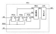
図7は、ディジタルフィルタ回路DFの一構成例(以下、「ディジタルフィルタ回路DFa」と符号する)を示す回路図であり、図8は、ディジタルフィルタ回路DFaの動作を説明するための図である。 FIG. 7 is a circuit diagram showing a configuration example of the digital filter circuit DF (hereinafter referred to as “digital filter circuit DFA”), and FIG. 8 is a diagram for explaining the operation of the digital filter circuit DFA. .
図7に示す通り、本構成例のディジタルフィルタ回路DFaは、DフリップフロップFF1a、FF2a、FF3aと、多数決部MAJと、ラッチ部LTCと、を有して成る。 As shown in FIG. 7, the digital filter circuit DFa of this configuration example includes D flip-flops FF1a, FF2a, and FF3a, a majority decision unit MAJ, and a latch unit LTC.
DフリップフロップFF1aのデータ入力端(D)には、アナログフィルタ回路AF2の出力パルス信号S2(フィルタリング処理が為されたスタートパルス信号SP)が入力されている。DフリップフロップFF2aのデータ入力端(D)には、DフリップフロップFF1aの出力信号Q1が入力されている。DフリップフロップFF3aのデータ入力端(D)には、DフリップフロップFF2aの出力信号Q2が入力されている。 The output pulse signal S2 of the analog filter circuit AF2 (start pulse signal SP subjected to the filtering process) is input to the data input terminal (D) of the D flip-flop FF1a. The output signal Q1 of the D flip-flop FF1a is input to the data input terminal (D) of the D flip-flop FF2a. The output signal Q2 of the D flip-flop FF2a is input to the data input terminal (D) of the D flip-flop FF3a.
一方、DフリップフロップFF1a、FF2a、FF3aの各クロック入力端には、いずれも、アナログフィルタ回路AF1の出力パルス信号S1(フィルタリング処理が為されたクロックパルス信号CLK)に同期した内部クロックパルス信号ICLK(出力パルス信号S1の逓倍信号)が入力されている。 On the other hand, each clock input terminal of the D flip-flops FF1a, FF2a, and FF3a has an internal clock pulse signal ICLK that is synchronized with the output pulse signal S1 of the analog filter circuit AF1 (clock pulse signal CLK subjected to filtering processing). (Multiplication signal of output pulse signal S1) is input.
すなわち、DフリップフロップFF1a、FF2a、FF3aでは、上記の内部クロックパルス信号ICLKの立上がりエッジにて、各々の入力信号S2、Q1、Q2がサンプリングされることになる(サンプリング周期t1)。 That is, in the D flip-flops FF1a, FF2a, and FF3a, the input signals S2, Q1, and Q2 are sampled at the rising edge of the internal clock pulse signal ICLK (sampling period t1).
多数決部MAJは、DフリップフロップFF1a、FF2a、FF3aの出力信号Q1〜Q3を多数決して出力する手段である。より具体的に述べると、多数決部MAJは、出力信号Q1〜Q3のうち、2つ以上がハイレベルであれば、多数決信号M1をハイレベルとし、逆に、2つ以上がローレベルであれば、多数決信号M1をローレベルとする。 The majority decision unit MAJ is means for never outputting a large number of output signals Q1 to Q3 of the D flip-flops FF1a, FF2a, and FF3a. More specifically, the majority decision unit MAJ sets the majority decision signal M1 to a high level if two or more of the output signals Q1 to Q3 are at a high level, and conversely if two or more are low levels. Then, the majority signal M1 is set to a low level.
ラッチ部LTCは、出力パルス信号S1の立上がりエッジにて、多数決信号M1をラッチし、そのラッチ出力を出力パルス信号S2’(フィルタリング処理、タイミング調整処理が為されたスタートパルス信号SP)として、ロジック部LGに送出する手段である。 The latch unit LTC latches the majority signal M1 at the rising edge of the output pulse signal S1, and uses the latch output as the output pulse signal S2 ′ (start pulse signal SP subjected to filtering processing and timing adjustment processing). It is means for sending to the part LG.
上記構成であれば、ディジタルフィルタ回路DFを簡易に構成することが可能となる。 With the above configuration, the digital filter circuit DF can be easily configured.
次に、ディジタルフィルタ回路DFの別構成例及びその動作について詳細に説明する。 Next, another configuration example and operation of the digital filter circuit DF will be described in detail.
図9は、ディジタルフィルタ回路DFの別構成例(以下、「ディジタルフィルタ回路DFb」と符号する)を示す回路図であり、図10は、ディジタルフィルタ回路DFbの動作を説明するための図である。 FIG. 9 is a circuit diagram showing another configuration example of the digital filter circuit DF (hereinafter referred to as “digital filter circuit DFb”), and FIG. 10 is a diagram for explaining the operation of the digital filter circuit DFb. .
図9に示す通り、本構成例のディジタルフィルタ回路DFbは、DフリップフロップFF1b、FF2b、FF3bと、多数決部MAJと、ラッチ部LTCと、を有して成る。 As shown in FIG. 9, the digital filter circuit DFb of this configuration example includes D flip-flops FF1b, FF2b, and FF3b, a majority decision unit MAJ, and a latch unit LTC.
DフリップフロップFF1bのクロック入力端には、アナログフィルタ回路AF1の出力パルス信号S1(フィルタリング処理が為されたクロックパルス信号CLK)が入力されている。DフリップフロップFF2bのクロック入力端には、第1内部クロックパルス信号ICLK1(出力パルス信号S1を所定時間t2だけ遅らせた遅延パルス信号)が入力されている。DフリップフロップFF3bの入力端には、第2内部クロックパルス信号ICLK2(第1内部クロックパルス信号ICLK1を所定時間t2だけ遅らせた遅延パルス信号)が入力されている。 The output pulse signal S1 (clock pulse signal CLK subjected to filtering processing) of the analog filter circuit AF1 is input to the clock input terminal of the D flip-flop FF1b. A first internal clock pulse signal ICLK1 (a delayed pulse signal obtained by delaying the output pulse signal S1 by a predetermined time t2) is input to the clock input terminal of the D flip-flop FF2b. A second internal clock pulse signal ICLK2 (a delayed pulse signal obtained by delaying the first internal clock pulse signal ICLK1 by a predetermined time t2) is input to the input terminal of the D flip-flop FF3b.
一方、DフリップフロップFF1b、FF2b、FF3bのデータ入力端(D)には、いずれも、アナログフィルタ回路AF2の出力パルス信号S2(フィルタリング処理が為されたスタートパルス信号SP)が入力されている。 On the other hand, all of the data input terminals (D) of the D flip-flops FF1b, FF2b, and FF3b are supplied with the output pulse signal S2 of the analog filter circuit AF2 (start pulse signal SP subjected to the filtering process).
すなわち、DフリップフロップFF1b、FF2b、FF3bでは、出力パルス信号S1、及び、第1、第2内部クロックパルス信号ICLK1、ICLK2の各立上がりエッジにて、各々の入力信号S2がサンプリングされることになる。 That is, in the D flip-flops FF1b, FF2b, and FF3b, each input signal S2 is sampled at each rising edge of the output pulse signal S1 and the first and second internal clock pulse signals ICLK1 and ICLK2. .
多数決部MAJは、DフリップフロップFF1b、FF2b、FF3bの出力信号Q1〜Q3を多数決して出力する手段である。より具体的に述べると、多数決部MAJは、出力信号Q1〜Q3のうち、2つ以上がハイレベルであれば、多数決信号M1をハイレベルとし、逆に、2つ以上がローレベルであれば、多数決信号M1をローレベルとする。 The majority decision unit MAJ is means for never outputting a large number of output signals Q1 to Q3 of the D flip-flops FF1b, FF2b, and FF3b. More specifically, the majority decision unit MAJ sets the majority decision signal M1 to a high level if two or more of the output signals Q1 to Q3 are at a high level, and conversely if two or more are low levels. The majority signal M1 is set to a low level.
ラッチ部LTCは、出力パルス信号S1の立上がりエッジにて、多数決信号M1をラッチし、そのラッチ出力を出力パルス信号S2’(フィルタリング処理、タイミング調整処理が為されたスタートパルス信号SP)として、ロジック部LGに送出する手段である。 The latch unit LTC latches the majority signal M1 at the rising edge of the output pulse signal S1, and uses the latch output as the output pulse signal S2 ′ (start pulse signal SP subjected to filtering processing and timing adjustment processing). It is means for sending to the part LG.
上記構成であれば、出力パルス信号S1を逓倍することなく、ディジタルフィルタ回路DFを構成することが可能となるので、先の構成例に比べて、装置規模や消費電力を縮小することが可能となる。 With the above configuration, it is possible to configure the digital filter circuit DF without multiplying the output pulse signal S1, so that the device scale and power consumption can be reduced compared to the previous configuration example. Become.
なお、上記の実施形態では、CISモジュールのイメージセンサICに本発明を適用した構成を例示して説明を行ったが、本発明に係るアナログフィルタ回路の適用対象はこれに限定されるものではなく、レンズ結像方式のイメージセンサや、その他の信号処理装置についても、そのフィルタ手段として広く適用することが可能である。 In the above embodiment, the configuration in which the present invention is applied to the image sensor IC of the CIS module has been described as an example. However, the application target of the analog filter circuit according to the present invention is not limited to this. Also, the lens imaging type image sensor and other signal processing apparatuses can be widely applied as filter means.
また、本発明の構成は、上記実施形態のほか、発明の主旨を逸脱しない範囲で種々の変更を加えることが可能である。 The configuration of the present invention can be variously modified in addition to the above-described embodiment without departing from the spirit of the invention.
例えば、上記の実施形態では、アナログフィルタ回路を電界効果トランジスタで構成した場合を例示して説明を行ったが、本発明の構成はこれに限定されるものではなく、電界効果トランジスタに代えて、バイポーラトランジスタを用いても構わない。なお、その際には、Pチャネル型電界効果トランジスタに代えてPNP型バイポーラトランジスタを用いればよく、また、Nチャネル型電界効果トランジスタに代えてNPN型バイポーラトランジスタを用いればよい。また、各端子の接続に際しては、ソースがエミッタに相当し、ドレインがコレクタに相当し、ゲートがベースに相当するように、適宜接続すればよい。 For example, in the above embodiment, the case where the analog filter circuit is configured by a field effect transistor has been described as an example, but the configuration of the present invention is not limited to this, and instead of the field effect transistor, Bipolar transistors may be used. In this case, a PNP bipolar transistor may be used instead of the P channel field effect transistor, and an NPN bipolar transistor may be used instead of the N channel field effect transistor. In addition, the terminals may be connected appropriately so that the source corresponds to the emitter, the drain corresponds to the collector, and the gate corresponds to the base.
また、上記の第2実施形態では、スタートパルス信号SPが入力されるアナログフィルタ回路AF2の後段にのみ、ディジタルフィルタ回路DFを設けた構成を例に挙げて説明を行ったが、ディジタルフィルタ回路の挿入位置はこれに限定されるものではなく、他の信号入力経路にもディジタルフィルタ回路を挿入することは可能である。 In the second embodiment, the configuration in which the digital filter circuit DF is provided only in the subsequent stage of the analog filter circuit AF2 to which the start pulse signal SP is input has been described as an example. The insertion position is not limited to this, and it is possible to insert a digital filter circuit in another signal input path.
本発明は、アナログフィルタ回路のフィルタ定数を高精度かつ広範囲に設定するための技術であって、例えば、イメージセンサ及びイメージセンサモジュールの読取精度向上を図る上で有用な技術である。 The present invention is a technique for setting a filter constant of an analog filter circuit with high accuracy and in a wide range, and is a technique useful for improving the reading accuracy of, for example, an image sensor and an image sensor module.
1 イメージセンサモジュール(CISモジュール)
11(11a、11b)、12、13、…、1n イメージセンサIC
2 セット基板
3 フレキシブルケーブル
L1〜L3 信号ライン
T1〜T3 パッド
AF1〜AF3 アナログフィルタ回路
DF(DFa、DFb) ディジタルフィルタ回路
LG ロジック部
SN 受光素子列
I1 第1定電流源
I2 第2定電流源
CM1 第1カレントミラー部
CM2 第2カレントミラー部
P1〜P3 Pチャネル型電界効果トランジスタ
N1〜N3 Nチャネル型電界効果トランジスタ
C1 コンデンサ
BUF1 入力バッファ
BUF2 出力バッファ
INV1〜INV4 インバータ
FF1a〜FF3a、FF1b〜FF3b Dフリップフロップ
MAJ 多数決部
LTC ラッチ部1 Image sensor module (CIS module)
11 (11a, 11b), 12, 13,..., 1n image sensor IC
2 set
Claims (6)
Translated fromJapanesePriority Applications (2)
| Application Number | Priority Date | Filing Date | Title |
|---|---|---|---|
| JP2005268047AJP4712497B2 (en) | 2005-09-15 | 2005-09-15 | Filter circuit, and image sensor, image sensor module, and image reading apparatus using the same |
| US11/521,795US7773271B2 (en) | 2005-09-15 | 2006-09-15 | Filter circuit, and image sensor, image sensor module, and image reading apparatus provided therewith |
Applications Claiming Priority (1)
| Application Number | Priority Date | Filing Date | Title |
|---|---|---|---|
| JP2005268047AJP4712497B2 (en) | 2005-09-15 | 2005-09-15 | Filter circuit, and image sensor, image sensor module, and image reading apparatus using the same |
Publications (2)
| Publication Number | Publication Date |
|---|---|
| JP2007081914A JP2007081914A (en) | 2007-03-29 |
| JP4712497B2true JP4712497B2 (en) | 2011-06-29 |
Family
ID=37893357
Family Applications (1)
| Application Number | Title | Priority Date | Filing Date |
|---|---|---|---|
| JP2005268047AExpired - Fee RelatedJP4712497B2 (en) | 2005-09-15 | 2005-09-15 | Filter circuit, and image sensor, image sensor module, and image reading apparatus using the same |
Country Status (2)
| Country | Link |
|---|---|
| US (1) | US7773271B2 (en) |
| JP (1) | JP4712497B2 (en) |
Families Citing this family (3)
| Publication number | Priority date | Publication date | Assignee | Title |
|---|---|---|---|---|
| JP4670675B2 (en)* | 2006-02-16 | 2011-04-13 | ソニー株式会社 | Drive circuit for charge transfer unit and drive method for charge transfer unit |
| JP5048459B2 (en)* | 2007-11-09 | 2012-10-17 | 株式会社セイコーアイ・インフォテック | Image reading device |
| EP2494783A4 (en) | 2009-10-30 | 2013-04-10 | Agency Science Tech & Res | METHODS, DEVICES AND COMPUTER-READABLE MEDIA FOR PROCESSING A DIGITAL IMAGE |
Family Cites Families (16)
| Publication number | Priority date | Publication date | Assignee | Title |
|---|---|---|---|---|
| US4982294A (en)* | 1987-07-24 | 1991-01-01 | Eastman Kodak Company | Apparatus for enhancing and thresholding scanned microfilm images and methods for use therein |
| JPH0559995A (en) | 1991-08-31 | 1993-03-09 | Toyota Autom Loom Works Ltd | Rotational speed control device for internal combustion engine on vehicle |
| JPH0589265A (en)* | 1991-09-30 | 1993-04-09 | Nec Kansai Ltd | Integrating circuit |
| JPH05175800A (en)* | 1991-12-21 | 1993-07-13 | Nissan Motor Co Ltd | Noise elimination circuit |
| JPH06176144A (en)* | 1992-12-07 | 1994-06-24 | Ricoh Co Ltd | Image processing device |
| JP3157461B2 (en)* | 1996-05-31 | 2001-04-16 | 三洋電機株式会社 | Smoothing circuit |
| JPH10126228A (en) | 1996-10-17 | 1998-05-15 | Nec Eng Ltd | Digital waveform shaping circuit |
| JPH11195963A (en) | 1997-12-26 | 1999-07-21 | Casio Comput Co Ltd | Digital filter circuit |
| JP2002185309A (en) | 2000-12-18 | 2002-06-28 | Hitachi Ltd | Data holding circuit, semiconductor device, and method of designing semiconductor device |
| JP3668128B2 (en)* | 2000-12-20 | 2005-07-06 | 株式会社日立製作所 | Filter circuit |
| JP4151232B2 (en)* | 2001-04-23 | 2008-09-17 | 日本電気株式会社 | Shading correction circuit and method |
| KR100510532B1 (en)* | 2003-06-10 | 2005-08-26 | 삼성전자주식회사 | Adaptive noise reduction filter for Bayer pattern color signal, digital image signal processor having it, and method thereof |
| JP2005210441A (en)* | 2004-01-23 | 2005-08-04 | Sanyo Electric Co Ltd | Image signal processing device |
| JP4318553B2 (en)* | 2004-01-23 | 2009-08-26 | 三洋電機株式会社 | Image signal processing device |
| US20060115159A1 (en)* | 2004-11-30 | 2006-06-01 | Astrit Rexhepi | Boundary detection for images using coocurrence matrices |
| JP5045421B2 (en)* | 2007-12-21 | 2012-10-10 | ソニー株式会社 | Imaging apparatus, color noise reduction method, and color noise reduction program |
- 2005
- 2005-09-15JPJP2005268047Apatent/JP4712497B2/ennot_activeExpired - Fee Related
- 2006
- 2006-09-15USUS11/521,795patent/US7773271B2/enactiveActive
Also Published As
| Publication number | Publication date |
|---|---|
| US7773271B2 (en) | 2010-08-10 |
| US20070070215A1 (en) | 2007-03-29 |
| JP2007081914A (en) | 2007-03-29 |
Similar Documents
| Publication | Publication Date | Title |
|---|---|---|
| JP5206423B2 (en) | Image reading apparatus, image forming apparatus, and sample / hold control method | |
| EP2442546B1 (en) | Signal buffer circuit, sensor control board, image scanner, and image forming apparatus | |
| KR101166461B1 (en) | A/d conversion apparatus, solid-state image capturing apparatus and electronic information device | |
| JP5476876B2 (en) | Sensor driving circuit, driver device, image reading device, and image forming device | |
| US7889254B2 (en) | Photoelectric conversion apparatus and contact-type image sensor | |
| CN100542225C (en) | Image pickup device and image reading device using the image pickup device | |
| JP6736906B2 (en) | Solid-state imaging device and image reading device | |
| EP3598740B1 (en) | Image sensor and output compensation circuit of image sensor | |
| JP2007035726A (en) | Semiconductor device, module and electronic device | |
| US9362896B2 (en) | Chip, multichip module, and apparatus provided with the same | |
| US7863946B2 (en) | Electric signal outputting apparatus with a switching part, an impedance matching part, and an auxiliary switching part | |
| US20110298955A1 (en) | Clock multiplying circuit, solid-state imaging device, and phase-shift circuit | |
| JP4712497B2 (en) | Filter circuit, and image sensor, image sensor module, and image reading apparatus using the same | |
| US20040190087A1 (en) | Image sensor, image reading device, and method for setting resolution | |
| US7995250B2 (en) | Image-reading device employing contact image sensor | |
| JP3975960B2 (en) | Reading apparatus and reading method | |
| US8295420B2 (en) | Image reading device | |
| JP2009231941A (en) | Sample-hold circuit and ccd image sensor | |
| US20040190083A1 (en) | Image sensor, image reading device, and image resolution setting method | |
| CN108632494A (en) | Image read-out and semiconductor device | |
| US20180262640A1 (en) | Image reading device and semiconductor device | |
| US7492492B2 (en) | Image sensor, reading device and method for setting particular mode | |
| JP4383326B2 (en) | Image reading apparatus and image forming apparatus | |
| JP4710728B2 (en) | Image reading apparatus, image reading apparatus control method, and image reading apparatus control program | |
| JP2023034507A (en) | Semiconductor device, image reading device, and method for controlling semiconductor device |
Legal Events
| Date | Code | Title | Description |
|---|---|---|---|
| A621 | Written request for application examination | Free format text:JAPANESE INTERMEDIATE CODE: A621 Effective date:20080808 | |
| A01 | Written decision to grant a patent or to grant a registration (utility model) | Free format text:JAPANESE INTERMEDIATE CODE: A01 Effective date:20110322 | |
| A61 | First payment of annual fees (during grant procedure) | Free format text:JAPANESE INTERMEDIATE CODE: A61 Effective date:20110323 | |
| LAPS | Cancellation because of no payment of annual fees |