JP4712157B2 - Non-contact data carrier - Google Patents
Non-contact data carrierDownload PDFInfo
- Publication number
- JP4712157B2 JP4712157B2JP2000135034AJP2000135034AJP4712157B2JP 4712157 B2JP4712157 B2JP 4712157B2JP 2000135034 AJP2000135034 AJP 2000135034AJP 2000135034 AJP2000135034 AJP 2000135034AJP 4712157 B2JP4712157 B2JP 4712157B2
- Authority
- JP
- Japan
- Prior art keywords
- chip
- antenna
- resin base
- base material
- data carrier
- Prior art date
- Legal status (The legal status is an assumption and is not a legal conclusion. Google has not performed a legal analysis and makes no representation as to the accuracy of the status listed.)
- Expired - Fee Related
Links
Images


Landscapes
- Credit Cards Or The Like (AREA)
Description
Translated fromJapanese【0001】
【発明の属する技術分野】
本発明は樹脂基材とアンテナとICチップとを有する非接触式データキャリアに係り、とりわけICチップの実装を容易に行うことができる非接触式データキャリアに関する。
【0002】
【従来の技術】
従来より非接触式データキャリアが、物流システム等において用いられている。このような非接触式データキャリアは、例えば製品の包装箱あるいは製品自体に貼付されて使用される。
【0003】
非接触式データキャリアは、一般に樹脂基材と、樹脂基材上に設けられた金属製アンテナコイルと、アンテナコイルに接続されたICチップとを備えている。
【0004】
非接触式データキャリアに対して読取機側から電磁波が発せられると、アンテナコイルに誘導電圧が発生し、ICチップを作動させるようになっている。
【0005】
【発明が解決しようとする課題】
非接触式データキャリアは、上述のように樹脂基材上に設けられた金属製アンテナコイルと、このアンテナコイルに接続されたICチップとを備えているが、ICチップをアンテナコイルに実装する際、アンテナコイル上の所定位置にICチップを配置し、このICチップをアンテナコイルに加熱圧着させている。
【0006】
しかしながらICチップをアンテナコイル上の所定位置に位置決めして配置することはむずかしく、このためICチップの実装作業に時間がかかるのが実情である。
【0007】
本発明はこのような点を考慮してなされたものであり、ICチップを容易にかつ簡単に実装することができる非接触式データキャリアを提供することを目的とする。
【0008】
【課題を解決するための手段】
本発明は、樹脂基材と、樹脂基材に設けられたアンテナと、アンテナに接続されたICチップ体と、を備え、ICチップ体は、絶縁性基板と、絶縁性基板上に設けられた導電パターン層と、導電パターン層に接続されたICチップとを有し、ICチップ体の導電パターン層および絶縁性基板、アンテナおよび樹脂基材を貫通して導通カシメ部材が設けられ、この導通カシメ部材はかしめられて形成されてアンテナと導電パターン層を導通させることを特徴とする非接触式データキャリアである。
【0009】
本発明によれば、絶縁性基板と、導電パターン層と、ICチップとからなるICチップ体を予め作製し、導電パターン層をアンテナに接続させた状態でICチップ体を樹脂基材に設ける。このためアンテナの所定位置にICチップを位置決め配置する必要はなく、ICチップの実装が容易となる。
【0010】
【発明の実施の形態】
以下、図面を参照して本発明の実施の形態について説明する。図1乃至図3は本発明による非接触式データキャリアの第1の実施の形態を示す図である。
【0011】
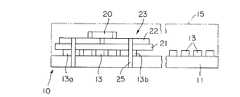
図1乃至図3に示すように、例えばICカードまたはICタグ等の非接触式データキャリア10は、PET製の樹脂基材11と、樹脂基材11上面(樹脂基材11の一側)の略全域にフォトレジスト層(図示せず)を用いてエッチングにより形成されたアルミ製の金属製アンテナコイル13と、アンテナコイル13上に設けられたICチップ体23とを備えている。
【0012】
このうちICチップ体23は絶縁性基板21と、絶縁性基板21上に設けられた導電パターン層22と、導電パターン層22に接続されたICチップ20とを有している。またICチップ体23の導電パターン層22は、後述のように導通カシメ部材25を介してアンテナコイル13の一対の端部13a,13bに接続されている。なおアンテナコイル13の代わりに、図5に示す面積受送信型のアンテナ33を用いてもよい。
【0013】
また、樹脂基材11上面には、ICチップ体23をアンテナコイル13上に設ける際の強度補強を図るため、金属板からなる金属補強部材26が設けられている。
【0014】
なおアンテナコイル13の一対の端部13a,13bは、アンテナコイル13の内側と外側に各々配置されている。
【0015】
また図1に示すように、樹脂基材11の上面にはアンテナコイル13およびICチップ体23を覆って第1保護層15が設けられている。
【0016】
次に各部の材料および形状について説明する。
【0017】
樹脂基材11としては、例えばポリエステル、ポリエチレン、ポリプロピレン、ポリイミド等のプラスチックフィルムの他、紙または不織布等が使用できるが、耐薬品性、耐熱性等からポリエステル、ポリイミドが主に用いられる。通常アンテナコイル13の形状は40mm×40mm程度となっているが、使用用途、必要性能によりアンテナコイル13をカード状等に形成してもよい。また樹脂基材11の厚さは30〜200μmとなっている。
【0018】
また金属製アンテナコイル13は、アルミ製となっており、その厚さは5〜100μ程度となっているが、コスト・電気的特性から、15〜30μmが好ましい。さらにICチップ20は、大きさ1.5mm×1.5mm角、厚さ約180μmのものが用いられる。
【0019】
金属補強部材26はアルミ製となってアンテナコイル13と同時に形成されるが、他の金属製のものを用いても良い。
【0020】
また第1保護層15は、例えばポリエステル、PVC、ポリイミド、ポリプロピレン、ポリエチレン等が用いられるが、強度、耐熱性等の点でポリエステル等が主に用いられる。
【0021】
このような構成からなる非接触式データキャリア10は、例えば製品の包装箱あるいは製品自体に貼付されて使用されるものである。すなわち、図示しない物流システムの読取機からの電磁波によりアンテナコイル13に誘導起電力が生じ、続いてアンテナコイル13に導電カシメ部材25および導電パターン層22を介して接続されたICチップ20が作動し、ICチップ20からの情報が読取機側へ送信されるようになっている。
【0022】
次にこのような構成からなる非接触式データキャリアの製造方法について説明する。まず樹脂基材11が準備され、樹脂基材11の上面にフォトレジスト層を用いたエッチング法によりアンテナコイル13が形成される。
【0023】
同時に樹脂基材11の上面にエッチング法により金属補強部材26が設けられる。なお、金属製補強部材26を樹脂基板11上に貼り付けにより設けてもよい。
【0024】
他方、図2に示すように、絶縁性基材21上に導電パターン層22を設け、さらに導電パターン層22上にICチップ20を接続することにより予めICチップ体23を作製しておく。
【0025】
次に図1に示すように、樹脂基材11およびアンテナコイル13上に、ICチップ体23が搭載される。次にICチップ体23の導電パターン層22および絶縁性基板21と、コイル13の一対の端部13a,13bと、樹脂基材11とを貫通して導通カシメ部材25が設けられ、導通カシメ部材25がかしめられて、樹脂基材11およびアンテナコイル13が接合される。
【0026】
この場合、コイル13の一対の端部13a,13bは、導電パターン層22を介してICチップ20に電気的に導通する。なお、電通カシメ部材25をかしめる際、樹脂基材11上に金属補強部材26が形成されているので、導通カシメ部材25に加わる力をこの金属補強部材26により受けることができ、樹脂基材11のたるみおよび収縮が防止される。
【0027】
その後、樹脂基材11の上面側においてアンテナコイル13およびICチップ体23上に第1保護層15が重ねられ、ラミネート法により、アンテナコイル13およびICチップ体23上に、第1保護層15が圧着して固着される。
【0028】
以上説明したように、本実施の形態によれば、予め絶縁性基板21と導電パターン層22とICチップ20とからなるICチップ体23を作製しておき、このICチップ体23を導通カシメ部材25により樹脂基材11上のアンテナコイル13に接続したので、アンテナコイル13とICチップ20との位置決めを行うことなくICチップ20の実装作業を行うことができる。このためICチップ20の実装作業を容易かつ簡単に行うことができる。
【0029】
次に図4により、本発明の第2の実施の形態について説明する。図4に示す実施の形態は、絶縁性基板21と、導電パターン層22と、ICチップ20とからなるICチップ体23を樹脂基板11の下面に配置するとともに、絶縁性接着剤14を用いて貼付け、次にICチップ体23を導通カシメ部材25を用いて樹脂基材11に接合したものである。
【0030】
図4において、他の構成は、図1乃至図3に示す第1の実施の形態と略同一である。図4において、図1乃至図3に示す第1の実施の形態と同一部分には同一符号を符して詳細な説明は省略する。
【0031】
図4において、アンテナコイル13を覆って第1保護層15が設けられ、ICチップ体23を覆って第2保護層16が設けられている。
【0032】
次に図6および図7により、本発明の第3の実施の形態について説明する。図6および図7に示す実施の形態は、ICチップ体23の絶縁性基板21と、導電性パターン層22を細長状に構成したものであり、他の構成は図1乃至図3に示す第1の実施の形態を略同一である。
【0033】
図6および図7において、図1乃至図3に示す第1の実施の形態と同一部分には同一符号を符して詳細な説明は省略する。
【0034】
図6および図7に示すように、ICチップ体23の絶縁性基板21と導電性パターン層22は細長状に構成されているため、アンテナコイル13の一対の端部13a,13bが離れていてもICチップ体23を容易に一対の端部13a,13b間に接続することができる。
【0035】
【発明の効果】
以上のように本発明によれば、絶縁性基板と、導電パターン層と、ICチップとかなるICチップ体を予め作製し、このICチップ体を樹脂基材に接合するので、アンテナとICチップの位置決めを行う必要なく、容易かつ簡単にICチップを実装することができる。
【図面の簡単な説明】
【図1】本発明による非接触式データキャリアの第1の実施の形態を示す側面図。
【図2】ICチップ体を示す側面図。
【図3】本発明による非接触式データキャリアの第1の実施の形態を示す平面図。
【図4】本発明による非接触式データキャリアの第2の実施の形態を示す側面図。
【図5】面積受送信型のアンテナを示す図。
【図6】本発明による非接触データキャリアの第3の実施の形態を示す平面図。
【図7】ICチップ体の拡大図。
【符号の説明】
10 非接触式データキャリア
11 樹脂基材
13 アンテナコイル
15 第1保護層
16 第2保護層
20 ICチップ
21 絶縁性基板
22 導電パターン層
23 ICチップ体
25 導通カシメ部材
26 金属補強部材[0001]
BACKGROUND OF THE INVENTION
The present invention relates to a non-contact type data carrier having a resin substrate, an antenna, and an IC chip, and more particularly to a non-contact type data carrier capable of easily mounting an IC chip.
[0002]
[Prior art]
Conventionally, non-contact data carriers have been used in distribution systems and the like. Such a non-contact type data carrier is used by being attached to, for example, a product packaging box or the product itself.
[0003]
A non-contact type data carrier generally includes a resin base material, a metal antenna coil provided on the resin base material, and an IC chip connected to the antenna coil.
[0004]
When electromagnetic waves are emitted from the reader side to the non-contact type data carrier, an induced voltage is generated in the antenna coil, and the IC chip is operated.
[0005]
[Problems to be solved by the invention]
The non-contact type data carrier includes the metal antenna coil provided on the resin base as described above and the IC chip connected to the antenna coil. When the IC chip is mounted on the antenna coil, The IC chip is disposed at a predetermined position on the antenna coil, and this IC chip is heat-pressed to the antenna coil.
[0006]
However, it is difficult to position and arrange the IC chip at a predetermined position on the antenna coil. For this reason, it takes a long time to mount the IC chip.
[0007]
The present invention has been made in consideration of such points, and an object thereof is to provide a non-contact data carrier on which an IC chip can be easily and easily mounted.
[0008]
[Means for Solving the Problems]
The present invention includes a resin base material, an antenna provided on the resin base material, and an IC chip body connected to the antenna. The IC chip body is provided on the insulating substrate and the insulating substrate. The conductive pattern layer and an IC chip connected tothe conductive pattern layer are provided, and a conductive crimping member is provided through the conductive pattern layer of theIC chip body, the insulating substrate, the antenna, and the resin base material. The member is a non-contact type data carrier that isformed by caulking to electrically connect the antenna and the conductive pattern layer .
[0009]
According to the present invention, an IC chip body including an insulating substrate, a conductive pattern layer, and an IC chip is prepared in advance, and the IC chip body is provided on the resin base material in a state where the conductive pattern layer is connected to the antenna. For this reason, it is not necessary to position and arrange the IC chip at a predetermined position of the antenna, and the IC chip can be easily mounted.
[0010]
DETAILED DESCRIPTION OF THE INVENTION
Embodiments of the present invention will be described below with reference to the drawings. 1 to 3 are views showing a first embodiment of a contactless data carrier according to the present invention.
[0011]
As shown in FIGS. 1 to 3, for example, a
[0012]
Among these, the
[0013]
In addition, a
[0014]
The pair of
[0015]
As shown in FIG. 1, a first
[0016]
Next, the material and shape of each part will be described.
[0017]
As the resin base material 11, for example, a plastic film such as polyester, polyethylene, polypropylene, and polyimide, paper, or non-woven fabric can be used. However, polyester and polyimide are mainly used from the viewpoint of chemical resistance and heat resistance. Normally, the shape of the
[0018]
The
[0019]
The
[0020]
The first
[0021]
The non-contact
[0022]
Next, a method for manufacturing a non-contact type data carrier having such a configuration will be described. First, the resin base material 11 is prepared, and the
[0023]
At the same time, a
[0024]
On the other hand, as shown in FIG. 2, the
[0025]
Next, as shown in FIG. 1, an
[0026]
In this case, the pair of
[0027]
Thereafter, the first
[0028]
As described above, according to the present embodiment, the
[0029]
Next, a second embodiment of the present invention will be described with reference to FIG. In the embodiment shown in FIG. 4, an
[0030]
In FIG. 4, other configurations are substantially the same as those of the first embodiment shown in FIGS. 4, the same parts as those of the first embodiment shown in FIGS. 1 to 3 are denoted by the same reference numerals, and detailed description thereof is omitted.
[0031]
In FIG. 4, a first
[0032]
Next, a third embodiment of the present invention will be described with reference to FIGS. In the embodiment shown in FIGS. 6 and 7, the insulating
[0033]
6 and 7, the same parts as those of the first embodiment shown in FIGS. 1 to 3 are denoted by the same reference numerals, and detailed description thereof is omitted.
[0034]
As shown in FIGS. 6 and 7, since the insulating
[0035]
【The invention's effect】
As described above, according to the present invention, an IC chip body that is an insulating substrate, a conductive pattern layer, and an IC chip is prepared in advance, and this IC chip body is bonded to a resin substrate. An IC chip can be mounted easily and easily without the need for positioning.
[Brief description of the drawings]
FIG. 1 is a side view showing a first embodiment of a contactless data carrier according to the present invention.
FIG. 2 is a side view showing an IC chip body.
FIG. 3 is a plan view showing a first embodiment of a contactless data carrier according to the present invention.
FIG. 4 is a side view showing a second embodiment of a contactless data carrier according to the present invention.
FIG. 5 is a diagram showing an area receiving / transmitting antenna;
FIG. 6 is a plan view showing a third embodiment of a contactless data carrier according to the present invention.
FIG. 7 is an enlarged view of an IC chip body.
[Explanation of symbols]
DESCRIPTION OF
Claims (3)
Translated fromJapanese樹脂基材に設けられ一対の端部を有するアンテナと、
アンテナの一対の端部に接続されたICチップ体と、を備え、
ICチップ体は、絶縁性基板と、絶縁性基板上に設けられた導電パターン層と、導電パターン層に接続されたICチップとを有し、
ICチップ体の導電パターン層および絶縁性基板、アンテナの一対の端部および樹脂基材を貫通して導通カシメ部材が設けられ、この導通カシメ部材はかしめられて形成されてアンテナの一対の端部とICチップとの位置決めを行うことなくアンテナの一対の端部と導電パターン層を導通させてICチップを実装し、樹脂基材に金属補強板を設け、当該金属補強板はエッチング法によりアンテナと同時に、アンテナの一対の端部近傍に形成され、導通カシメ部材をかしめる際の力を受けて樹脂基材のたるみおよび収縮を防止することを特徴とする非接触式データキャリア。A resin substrate;
An antenna provided on a resin substrateand having a pair of ends ;
An IC chip body connected toa pair of ends of the antenna,
The IC chip body has an insulating substrate, a conductive pattern layer provided on the insulating substrate, and an IC chip connected to the conductive pattern layer,
A conductive caulking member is provided through the conductive pattern layer of the IC chip body and the insulating substrate,the pair of end portions of the antenna and the resin base material, and the conductive caulking member is formed by caulking to forma pair of end portions of the antenna. TheIC chip is mounted by conductingthe pair of end portions of the antenna and the conductive pattern layerwithout positioning the IC chip and the IC chip, and ametal reinforcing plate is provided on the resin base. At the same time, a non-contact type data carrier formed near the pair of end portions of the antenna and receiving a force when caulking the conductive caulking member to prevent sagging and shrinkage of the resin base material.
Priority Applications (1)
| Application Number | Priority Date | Filing Date | Title |
|---|---|---|---|
| JP2000135034AJP4712157B2 (en) | 2000-05-08 | 2000-05-08 | Non-contact data carrier |
Applications Claiming Priority (1)
| Application Number | Priority Date | Filing Date | Title |
|---|---|---|---|
| JP2000135034AJP4712157B2 (en) | 2000-05-08 | 2000-05-08 | Non-contact data carrier |
Publications (2)
| Publication Number | Publication Date |
|---|---|
| JP2001319203A JP2001319203A (en) | 2001-11-16 |
| JP4712157B2true JP4712157B2 (en) | 2011-06-29 |
Family
ID=18643198
Family Applications (1)
| Application Number | Title | Priority Date | Filing Date |
|---|---|---|---|
| JP2000135034AExpired - Fee RelatedJP4712157B2 (en) | 2000-05-08 | 2000-05-08 | Non-contact data carrier |
Country Status (1)
| Country | Link |
|---|---|
| JP (1) | JP4712157B2 (en) |
Families Citing this family (1)
| Publication number | Priority date | Publication date | Assignee | Title |
|---|---|---|---|---|
| CN110729605A (en)* | 2019-11-12 | 2020-01-24 | 杭州余杭电缆有限公司 | Plug with induction chip |
Family Cites Families (5)
| Publication number | Priority date | Publication date | Assignee | Title |
|---|---|---|---|---|
| JP3481663B2 (en)* | 1994-02-24 | 2003-12-22 | 三菱電機株式会社 | Circuit board and method of manufacturing the same |
| JPH0927363A (en)* | 1995-07-13 | 1997-01-28 | Nec Home Electron Ltd | Connector structure for multilayered printed circuit board |
| EP0998723B1 (en)* | 1997-07-28 | 2003-04-09 | Karl-Heinz Wendisch | Module and its use in a chip card |
| JP3951409B2 (en)* | 1998-02-12 | 2007-08-01 | 日立化成工業株式会社 | IC card and its manufacturing method |
| JP2000036023A (en)* | 1998-07-16 | 2000-02-02 | Toshiba Corp | Wireless card inlet and wireless card |
- 2000
- 2000-05-08JPJP2000135034Apatent/JP4712157B2/ennot_activeExpired - Fee Related
Also Published As
| Publication number | Publication date |
|---|---|
| JP2001319203A (en) | 2001-11-16 |
Similar Documents
| Publication | Publication Date | Title |
|---|---|---|
| KR100679502B1 (en) | RDF tag, antenna for RDF tag, antenna sheet for RDF tag, and RDF tag manufacturing method | |
| ES2364437T3 (en) | RFID LABEL THAT HAS A WINDOW WITH RELEASE COVER, AND MANUFACTURING METHOD. | |
| CN101233533B (en) | Storage medium with built-in antenna | |
| JP4692863B2 (en) | Disposable chip electronic device and manufacturing method | |
| KR100191975B1 (en) | Radio frequency circuit and memory in thin flexible package | |
| JP2008107947A (en) | RFID tag | |
| US20070095922A1 (en) | Information carrier, information recording medium, sensor, commodity management method | |
| CA2153440A1 (en) | Radio frequency identification tag | |
| US20060012482A1 (en) | Radio frequency identification tag having an inductively coupled antenna | |
| JP2006285911A (en) | RFID tag | |
| JP2010231763A (en) | IC card | |
| WO2001026910A1 (en) | Non-contact data carrier and ic chip | |
| JP4176244B2 (en) | Chip card | |
| JP4117989B2 (en) | IC tag | |
| KR100760505B1 (en) | Rfid tag set, rfid tag and rfid tag component | |
| JP4712157B2 (en) | Non-contact data carrier | |
| JP2003132331A (en) | Non-contact data carrier substrate and non-contact data carrier | |
| JP4620237B2 (en) | Non-contact data carrier with moisture and water resistance | |
| JP2001307049A (en) | Non-contact data carrier | |
| JP4418064B2 (en) | Non-contact data carrier | |
| JP5975936B2 (en) | Antenna sheet and manufacturing method thereof | |
| JP2001307050A (en) | Non-contact data carrier | |
| JP4593734B2 (en) | Non-contact data carrier device | |
| US10402713B1 (en) | RF transponder on adhesive transfer tape | |
| JP4614518B2 (en) | Non-contact data carrier |
Legal Events
| Date | Code | Title | Description |
|---|---|---|---|
| A621 | Written request for application examination | Free format text:JAPANESE INTERMEDIATE CODE: A621 Effective date:20070423 | |
| A977 | Report on retrieval | Free format text:JAPANESE INTERMEDIATE CODE: A971007 Effective date:20091215 | |
| A131 | Notification of reasons for refusal | Free format text:JAPANESE INTERMEDIATE CODE: A131 Effective date:20091222 | |
| A521 | Request for written amendment filed | Free format text:JAPANESE INTERMEDIATE CODE: A523 Effective date:20100219 | |
| A131 | Notification of reasons for refusal | Free format text:JAPANESE INTERMEDIATE CODE: A131 Effective date:20100528 | |
| A521 | Request for written amendment filed | Free format text:JAPANESE INTERMEDIATE CODE: A523 Effective date:20100721 | |
| A131 | Notification of reasons for refusal | Free format text:JAPANESE INTERMEDIATE CODE: A131 Effective date:20101022 | |
| A01 | Written decision to grant a patent or to grant a registration (utility model) | Free format text:JAPANESE INTERMEDIATE CODE: A01 Effective date:20110222 | |
| A61 | First payment of annual fees (during grant procedure) | Free format text:JAPANESE INTERMEDIATE CODE: A61 Effective date:20110323 | |
| LAPS | Cancellation because of no payment of annual fees |