JP4710216B2 - Thin film formation method - Google Patents
Thin film formation methodDownload PDFInfo
- Publication number
- JP4710216B2 JP4710216B2JP2003143701AJP2003143701AJP4710216B2JP 4710216 B2JP4710216 B2JP 4710216B2JP 2003143701 AJP2003143701 AJP 2003143701AJP 2003143701 AJP2003143701 AJP 2003143701AJP 4710216 B2JP4710216 B2JP 4710216B2
- Authority
- JP
- Japan
- Prior art keywords
- dielectric
- thin film
- metal atom
- base material
- electrode
- Prior art date
- Legal status (The legal status is an assumption and is not a legal conclusion. Google has not performed a legal analysis and makes no representation as to the accuracy of the status listed.)
- Expired - Fee Related
Links
Images


Classifications
- C—CHEMISTRY; METALLURGY
- C23—COATING METALLIC MATERIAL; COATING MATERIAL WITH METALLIC MATERIAL; CHEMICAL SURFACE TREATMENT; DIFFUSION TREATMENT OF METALLIC MATERIAL; COATING BY VACUUM EVAPORATION, BY SPUTTERING, BY ION IMPLANTATION OR BY CHEMICAL VAPOUR DEPOSITION, IN GENERAL; INHIBITING CORROSION OF METALLIC MATERIAL OR INCRUSTATION IN GENERAL
- C23C—COATING METALLIC MATERIAL; COATING MATERIAL WITH METALLIC MATERIAL; SURFACE TREATMENT OF METALLIC MATERIAL BY DIFFUSION INTO THE SURFACE, BY CHEMICAL CONVERSION OR SUBSTITUTION; COATING BY VACUUM EVAPORATION, BY SPUTTERING, BY ION IMPLANTATION OR BY CHEMICAL VAPOUR DEPOSITION, IN GENERAL
- C23C30/00—Coating with metallic material characterised only by the composition of the metallic material, i.e. not characterised by the coating process
- H—ELECTRICITY
- H05—ELECTRIC TECHNIQUES NOT OTHERWISE PROVIDED FOR
- H05H—PLASMA TECHNIQUE; PRODUCTION OF ACCELERATED ELECTRICALLY-CHARGED PARTICLES OR OF NEUTRONS; PRODUCTION OR ACCELERATION OF NEUTRAL MOLECULAR OR ATOMIC BEAMS
- H05H1/00—Generating plasma; Handling plasma
- H05H1/24—Generating plasma
- H05H1/26—Plasma torches
- H05H1/30—Plasma torches using applied electromagnetic fields, e.g. high frequency or microwave energy
- C—CHEMISTRY; METALLURGY
- C23—COATING METALLIC MATERIAL; COATING MATERIAL WITH METALLIC MATERIAL; CHEMICAL SURFACE TREATMENT; DIFFUSION TREATMENT OF METALLIC MATERIAL; COATING BY VACUUM EVAPORATION, BY SPUTTERING, BY ION IMPLANTATION OR BY CHEMICAL VAPOUR DEPOSITION, IN GENERAL; INHIBITING CORROSION OF METALLIC MATERIAL OR INCRUSTATION IN GENERAL
- C23C—COATING METALLIC MATERIAL; COATING MATERIAL WITH METALLIC MATERIAL; SURFACE TREATMENT OF METALLIC MATERIAL BY DIFFUSION INTO THE SURFACE, BY CHEMICAL CONVERSION OR SUBSTITUTION; COATING BY VACUUM EVAPORATION, BY SPUTTERING, BY ION IMPLANTATION OR BY CHEMICAL VAPOUR DEPOSITION, IN GENERAL
- C23C16/00—Chemical coating by decomposition of gaseous compounds, without leaving reaction products of surface material in the coating, i.e. chemical vapour deposition [CVD] processes
- C23C16/44—Chemical coating by decomposition of gaseous compounds, without leaving reaction products of surface material in the coating, i.e. chemical vapour deposition [CVD] processes characterised by the method of coating
- C23C16/50—Chemical coating by decomposition of gaseous compounds, without leaving reaction products of surface material in the coating, i.e. chemical vapour deposition [CVD] processes characterised by the method of coating using electric discharges
- C23C16/505—Chemical coating by decomposition of gaseous compounds, without leaving reaction products of surface material in the coating, i.e. chemical vapour deposition [CVD] processes characterised by the method of coating using electric discharges using radio frequency discharges
- C23C16/509—Chemical coating by decomposition of gaseous compounds, without leaving reaction products of surface material in the coating, i.e. chemical vapour deposition [CVD] processes characterised by the method of coating using electric discharges using radio frequency discharges using internal electrodes
- C—CHEMISTRY; METALLURGY
- C23—COATING METALLIC MATERIAL; COATING MATERIAL WITH METALLIC MATERIAL; CHEMICAL SURFACE TREATMENT; DIFFUSION TREATMENT OF METALLIC MATERIAL; COATING BY VACUUM EVAPORATION, BY SPUTTERING, BY ION IMPLANTATION OR BY CHEMICAL VAPOUR DEPOSITION, IN GENERAL; INHIBITING CORROSION OF METALLIC MATERIAL OR INCRUSTATION IN GENERAL
- C23C—COATING METALLIC MATERIAL; COATING MATERIAL WITH METALLIC MATERIAL; SURFACE TREATMENT OF METALLIC MATERIAL BY DIFFUSION INTO THE SURFACE, BY CHEMICAL CONVERSION OR SUBSTITUTION; COATING BY VACUUM EVAPORATION, BY SPUTTERING, BY ION IMPLANTATION OR BY CHEMICAL VAPOUR DEPOSITION, IN GENERAL
- C23C16/00—Chemical coating by decomposition of gaseous compounds, without leaving reaction products of surface material in the coating, i.e. chemical vapour deposition [CVD] processes
- C23C16/44—Chemical coating by decomposition of gaseous compounds, without leaving reaction products of surface material in the coating, i.e. chemical vapour deposition [CVD] processes characterised by the method of coating
- C23C16/54—Apparatus specially adapted for continuous coating
- C23C16/545—Apparatus specially adapted for continuous coating for coating elongated substrates
- C—CHEMISTRY; METALLURGY
- C23—COATING METALLIC MATERIAL; COATING MATERIAL WITH METALLIC MATERIAL; CHEMICAL SURFACE TREATMENT; DIFFUSION TREATMENT OF METALLIC MATERIAL; COATING BY VACUUM EVAPORATION, BY SPUTTERING, BY ION IMPLANTATION OR BY CHEMICAL VAPOUR DEPOSITION, IN GENERAL; INHIBITING CORROSION OF METALLIC MATERIAL OR INCRUSTATION IN GENERAL
- C23C—COATING METALLIC MATERIAL; COATING MATERIAL WITH METALLIC MATERIAL; SURFACE TREATMENT OF METALLIC MATERIAL BY DIFFUSION INTO THE SURFACE, BY CHEMICAL CONVERSION OR SUBSTITUTION; COATING BY VACUUM EVAPORATION, BY SPUTTERING, BY ION IMPLANTATION OR BY CHEMICAL VAPOUR DEPOSITION, IN GENERAL
- C23C4/00—Coating by spraying the coating material in the molten state, e.g. by flame, plasma or electric discharge
- C23C4/18—After-treatment
- H—ELECTRICITY
- H05—ELECTRIC TECHNIQUES NOT OTHERWISE PROVIDED FOR
- H05H—PLASMA TECHNIQUE; PRODUCTION OF ACCELERATED ELECTRICALLY-CHARGED PARTICLES OR OF NEUTRONS; PRODUCTION OR ACCELERATION OF NEUTRAL MOLECULAR OR ATOMIC BEAMS
- H05H1/00—Generating plasma; Handling plasma
- H05H1/24—Generating plasma
- H05H1/2406—Generating plasma using dielectric barrier discharges, i.e. with a dielectric interposed between the electrodes
- H05H1/2441—Generating plasma using dielectric barrier discharges, i.e. with a dielectric interposed between the electrodes characterised by the physical-chemical properties of the dielectric, e.g. porous dielectric
- B—PERFORMING OPERATIONS; TRANSPORTING
- B05—SPRAYING OR ATOMISING IN GENERAL; APPLYING FLUENT MATERIALS TO SURFACES, IN GENERAL
- B05D—PROCESSES FOR APPLYING FLUENT MATERIALS TO SURFACES, IN GENERAL
- B05D1/00—Processes for applying liquids or other fluent materials
- B05D1/62—Plasma-deposition of organic layers
- H—ELECTRICITY
- H05—ELECTRIC TECHNIQUES NOT OTHERWISE PROVIDED FOR
- H05H—PLASMA TECHNIQUE; PRODUCTION OF ACCELERATED ELECTRICALLY-CHARGED PARTICLES OR OF NEUTRONS; PRODUCTION OR ACCELERATION OF NEUTRAL MOLECULAR OR ATOMIC BEAMS
- H05H1/00—Generating plasma; Handling plasma
- H05H1/24—Generating plasma
- H05H1/47—Generating plasma using corona discharges
- H05H1/473—Cylindrical electrodes, e.g. rotary drums
- Y—GENERAL TAGGING OF NEW TECHNOLOGICAL DEVELOPMENTS; GENERAL TAGGING OF CROSS-SECTIONAL TECHNOLOGIES SPANNING OVER SEVERAL SECTIONS OF THE IPC; TECHNICAL SUBJECTS COVERED BY FORMER USPC CROSS-REFERENCE ART COLLECTIONS [XRACs] AND DIGESTS
- Y10—TECHNICAL SUBJECTS COVERED BY FORMER USPC
- Y10S—TECHNICAL SUBJECTS COVERED BY FORMER USPC CROSS-REFERENCE ART COLLECTIONS [XRACs] AND DIGESTS
- Y10S156/00—Adhesive bonding and miscellaneous chemical manufacture
- Y10S156/914—Differential etching apparatus including particular materials of construction
Landscapes
- Chemical & Material Sciences (AREA)
- Engineering & Computer Science (AREA)
- Physics & Mathematics (AREA)
- Plasma & Fusion (AREA)
- Metallurgy (AREA)
- Chemical Kinetics & Catalysis (AREA)
- Materials Engineering (AREA)
- Mechanical Engineering (AREA)
- Organic Chemistry (AREA)
- Spectroscopy & Molecular Physics (AREA)
- General Chemical & Material Sciences (AREA)
- Electromagnetism (AREA)
- Plasma Technology (AREA)
- Chemical Vapour Deposition (AREA)
- Physical Or Chemical Processes And Apparatus (AREA)
Description
Translated fromJapanese【0001】
【発明の属する技術分野】
本発明は、導電性母材の表面に誘電体を被覆した誘電体被覆電極、この誘電体被覆電極を備えたプラズマ放電処理装置及びこの誘電体被覆電極を用いた薄膜形成方法に関するものである。
【0002】
【従来の技術】
近年、液晶表示素子、半導体素子、光学素子などでは、導電膜、反射防止膜、帯電防止膜など多様な高機能膜が用いられている。これら高機能膜を形成する方法として、大気圧又は大気圧近傍の圧力下で放電し、反応性ガスをプラズマ励起し、電極間に配置した基材などの表面に薄膜を形成する方法(大気圧プラズマ法)が、特開平11−133205号、特開2000−185362号、特開平11−61406号、特開2000−147209号、同2000−121804号等に記載されている。
これら公報に開示される大気圧プラズマ法は、対向する電極間に、周波数が0.5〜100kHzである電圧を、電界の強さが1〜100V/cmとなるように印加し、放電プラズマを発生させるというものである。
【0003】
【発明が解決しようとする課題】
ところで、このような大気圧プラズマ法で使用される電極は、大気圧下で安定なグロー放電を得るために、電極表面には誘電体を被覆することが必要である。この誘電体は、所望の被誘電率を有していれば特に限定はないが、一般的に、ゴム、セラミック、ガラスなどが知られている。
本出願人は、特開平11−191500号公報において、金属母材上に、セラミックであるアルミナを溶射した誘電体被覆電極を大気圧プラズマ処理装置に使用する技術を提案している。このような誘電体被覆電極は、単にゴムやガラスを誘電体とした電極よりも耐久性が高く、基材表面のぬれ性や接着性等の表面性を変えたり、基材表面の汚れを除去したりといった、いわゆる表面処理には全く問題ない。
しかし、本発明者が大気圧プラズマ法で、高性能な薄膜を大面積で形成する場合について研究したところ、上記表面処理に比べ、より高周波、大電力の高周波電圧を印加することが必要であり、アルミナを溶射しただけの上記誘電体被覆電極では、その耐久性が不十分であることがわかった。具体的には、大気圧プラズマ処理装置の対向する誘電体被覆電極間に、周波数100kHzを越え、電力1W/cm2以上の高周波電圧を印加する必要があるという知見である。そこで、このようなハイパワーの電圧印加に耐えられる高耐久電極について鋭意研究した結果、誘電体の表面付近における組成をコントロールすることによって、ハイパワーの電圧を印加しても、長時間安定な放電状態を維持できる誘電体被覆電極を見いだした。
【0004】
本発明は、ハイパワーをかけても、安定な放電状態を長時間維持することのできる誘電体被覆電極、誘電体被覆電極を備えたプラズマ放電処理装置及び誘電体被覆電極を用いた薄膜形成方法を提供することを課題としている。
【0005】
【課題を解決するための手段】
上記課題を解決するために、請求項1の発明は、薄膜形成方法において、対向する電極間に反応性ガスを供給する工程と、大気圧又は大気圧近傍の圧力の下で、前記対向する電極間に15kWを超えるトータル電力で高周波電圧を印加して放電させることにより、前記反応性ガスをプラズマ状態とする工程と、前記対向する電極間に基材を供給し、前記プラズマ状態の反応性ガスに前記基材を晒すことによって前記基材の表面に薄膜を形成する工程と、を備え、前記対向する電極の少なくとも一方は、
導電性母材の表面に誘電体を被覆した誘電体被覆電極であって、
前記誘電体は、第1の金属原子と、第2の金属原子とを含有し、
ダイナミックSIMS測定による前記第1の金属原子のイオン強度及び前記第2の金属原子のイオン強度は、前記誘電体の最表面から所定の深さまでは前記第2の金属原子のイオン強度が前記第1の金属原子のイオン強度よりも大きく、前記所定の深さから前記導電性母材の表面までは前記第1の金属原子のイオン強度が前記第2の金属原子のイオン強度よりも大きく、
前記誘電体の厚みが0.5〜2mmであって膜厚変動が5%以下の誘電体被覆電極であって、さらに誘電体と導電性母材との線熱膨張係数の差が2×10⁻⁶/℃以下であることを特徴とする。
請求項2の発明は、薄膜形成方法において、対向する電極間に反応性ガスを供給する工程と、大気圧又は大気圧近傍の圧力の下で、前記対向する電極間に15kWを超えるトータル電力で高周波電圧を印加して放電させることにより、前記反応性ガスをプラズマ状態とする工程と、前記対向する電極間に基材を供給し、前記プラズマ状態の反応性ガスに前記基材を晒すことによって前記基材の表面に薄膜を形成する工程と、を備え、前記対向する電極は、
導電性母材の表面に誘電体を被覆した誘電体被覆電極であって、
前記誘電体は、第1の金属原子と、第2の金属原子とを含有し、
ダイナミックSIMS測定による前記第1の金属原子のイオン強度及び前記第2の金属原子のイオン強度は、前記誘電体の最表面から所定の深さまでは前記第2の金属原子のイオン強度が前記第1の金属原子のイオン強度よりも大きく、前記所定の深さから前記導電性母材の表面までは前記第1の金属原子のイオン強度が前記第2の金属原子のイオン強度よりも大きく、
前記誘電体の厚みが0.5〜2mmであって膜厚変動が5%以下の誘電体被覆電極であって、さらに誘電体と導電性母材との線熱膨張係数の差が2×10⁻⁶/℃以下であることを特徴とする。
【0006】
請求項3の発明は、請求項1又は2に記載の薄膜形成方法において、
前記所定の深さが1μm以上であることを特徴とする。
【0007】
請求項4の発明は、請求項3に記載の薄膜形成方法において、
前記第1の金属原子のイオン強度に対する前記第2の金属原子のイオン強度は、前記誘電体の最表面から前記所定の深さまで減少していることを特徴とする。
【0008】
請求項5の発明は、請求項3又は4に記載の薄膜形成方法において、
前記第1の金属原子がAlであり、前記第2の金属原子がSiであることを特徴とする。
【0009】
請求項6の発明は、請求項3〜5のいずれか一項に記載の薄膜形成方法において、
前記誘電体被覆電極が、前記導電性母材上に前記第1の金属原子を含有する材料を溶射した後に、前記第2の金属原子を含有する材料により封孔処理したものであることを特徴とする。
【0010】
請求項7の発明は、請求項6に記載の薄膜形成方法において、
前記第1の金属原子を含有する材料がアルミナであることを特徴とする。
【0011】
請求項8の発明は、請求項6又は7に記載の薄膜形成方法において、
前記封孔処理が、前記第2の金属原子を含有する材料を、前記溶射した後の電極表面に塗布し、ゾルゲル反応により硬化させるものであることを特徴とする。
【0012】
請求項9の発明は、請求項8に記載の薄膜形成方法において、
前記硬化させた第2の金属原子を含有する材料が、酸化珪素であることを特徴とする。
【0013】
請求項10の発明は、請求項3〜9のいずれか一項に記載の薄膜形成方法において、
前記誘電体の空隙率が10体積%以下であることを特徴とする。
【0015】
請求項11の発明は、請求項3〜10のいずれか一項に記載の薄膜形成方法において、
耐熱温度が100℃以上であることを特徴とする。
【0020】
【発明の実施の形態】
以下、本発明の実施の形態について説明する。
本発明の誘電体被覆電極は、金属等の導電性母材の表面に第1の金属原子を主成分とする材料を溶射して誘電体を被覆した後に、該誘電体の表層を第2の金属原子を主成分とする封孔剤で封孔処理したものであることが好ましい。
【0021】
この場合、ダイナミックSIMS測定による第1の金属原子のイオン強度及び第2の金属原子のイオン強度は、誘電体の最表面から所定の深さまでは第2の金属原子のイオン強度が第1の金属原子のイオン強度よりも大きく、前記所定の深さから導電性母材の表面までは第1の金属原子のイオン強度が第2の金属原子のイオン強度よりも大きい。
【0022】
また、前記第1の金属原子のイオン強度に対応する前記第2の金属原子のイオン強度は、誘電体の最表面から前記所定の深さまで減少していることが好ましい。減少しているとは、イオン濃度が、誘電体最表面に比べ、前記所定の深さにおいて低いことを指す。
最表面から前記所定の深さまでの濃度カーブは、連続的であることが好ましい。これは、第1の金属原子を主成分とする層と、第2の金属原子を主成分とする層とが、別々に分離して存在する場合(不連続)を排除するということにすぎない。濃度変化率一定で単調に減少しても良いし、濃度変化率は一定ではないが連続して負であっても良い。
このことは本発明の電極作成において、電極母材上の第1の金属原子を含有する材料の溶射膜表面から、第2の金属原子を含有する材料をしみこませるようにして形成することに起因している。詳細は不明だが、このような誘電体最表面からの組成をコントロールすることにより、電極全体の耐久性を向上させているのだと推定している。
なお、所定の深さとは、1μm以上であることが好ましい。
【0023】
このように、誘電体の最表面から所定の深さまでは第2の金属原子のイオン強度を大きくし、所定の深さから導電性母材の表面までは第1の金属原子のイオン強度を大きくすることによって、誘電体の最表面に形成されている空隙が第2の金属原子によって埋められて緻密な膜となると推定している。
一方、母材表面付近においては、第2の金属原子の侵入があまりなく、適当な空隙があるために、昇温による母材と誘電体の膨張差を吸収できるのではないかと考えられる。そのため、例えば100kHzを越えた高周波電圧で、かつ、1W/cm2以上の大電力を、対向する電極間に供給した場合、通常、電極の表面から絶縁破壊が生じるが、上述したように所定の深さまで第2の金属原子のイオン強度を大きくして緻密な膜とすることにより、絶縁破壊を防ぐことができる。よって、放電状態を長時間維持することが可能となる。
【0024】
ここで、ダイナミックSIMS測定(Dynamic Secondary Ion Mass Spectrometry:動的二次イオン質量分析測定)とは、試料表面にO2、Cs、Ar、Xeなどのイオンを照射し、表面から放出される二次イオンを検出する方法である。この方法は、連続的にイオンを照射し続けて試料を削りながら測定する方法であるため、深さ方向の分布状態の分析ができる。後述する実施例では、米Physical Electronics社製 ADEPT−1010を使用した。
このダイナミックSIMS測定において、第1の金属原子の金属イオンの検出強度が高く、検出器等が飽和してしまう可能性があるので、金属イオンの検出強度を弱めるようにFAP(Field Axis Potential)を調整して測定を行う。また、第2の金属原子の金属イオンの検出強度が高くて検出器等が飽和してしまう可能性がある場合にも、金属イオンの検出強度を弱めるようにFAPを調整して測定を行うとよい。
【0025】
また、本発明の誘電体被覆電極としては、導電性母材上の少なくとも放電面に誘電体を被覆したものである。つまり、後述する薄膜形成装置(プラズマ放電処理装置)に備えた場合に、少なくとも対向する印加電極とアース電極のどちらか片側に誘電体を被覆すること、好ましくは、印加電極とアース電極の両方に誘電体を被覆することである。
【0026】
本発明の誘電体被覆電極に用いられる誘電体、すなわち前記第1の金属原子を含有する材料としては、具体的には、比誘電率が6〜45の無機化合物であることが好ましく、また、このような誘電体としては、アルミナ、窒化珪素等のセラミックス等がある。この中では、セラミックスを溶射したものが好ましい。特にアルミナを溶射したものが好ましい。
【0027】
上記、導電性母材に対し、セラミックスを誘電体として高密度に、高密着に溶射する方法としては、大気プラズマ溶射法が挙げられる。大気プラズマ溶射法は、セラミックス等の微粉末、ワイヤ等をプラズマ熱源中に投入し、溶融又は半溶融状態の微粒子として被覆対象の導電性母材に吹き付け、皮膜を形成させる技術である。
【0028】
プラズマ熱源とは、分子ガスを高温にし、原子に解離させ、さらにエネルギーを与えて電子を放出させた高温のプラズマガスである。このプラズマガスの噴射速度は大きく、従来のアーク溶射やフレーム溶射に比べて、溶射材料が高速で導電性母材に衝突するため、密着強度が高く、高密度な被膜を得ることができる。
詳しくは、特開2000−301655号公報に記載の高温被曝部材に熱遮蔽皮膜を形成する溶射方法を参照することができる。この方法によれば、被覆する誘電体(セラミック溶射膜)の空隙率を10体積%以下、さらには8体積%以下とすることが可能である。
【0029】
このように被覆されたセラミックス等の溶射膜(誘電体)の表面に行う封孔処理は、前記第2の金属原子を含有する材料、すなわち無機化合物で行うことが好ましい。無機化合物としては、金属酸化物が好ましく、この中では特に酸化ケイ素(SiOx)を主成分として含有するものが好ましい。封孔処理を行うことによって、誘電体の空隙率をより低減させることができる。
【0030】
また、封孔処理の無機化合物は、ゾルゲル反応により硬化して形成したものであることが好ましい。封孔処理の無機化合物が金属酸化物を主成分とするものである場合には、金属アルコキシド等を封孔液として前記セラミック溶射膜上に塗布し、ゾルゲル反応により硬化する。無機化合物がシリカを主成分とするものの場合には、アルコキシシランを封孔液として用いることが好ましい。
【0031】
ここでゾルゲル反応の促進には、エネルギー処理を用いることが好ましい。エネルギー処理としては、熱硬化(好ましくは200℃以下)や、UV照射などがある。更に封孔処理の仕方として、封孔液を希釈し、コーティングと硬化を逐次で数回繰り返すと、よりいっそう無機質化が向上し、劣化の無い緻密な電極ができる。
【0032】
本発明の誘電体被覆電極の金属アルコキシド等を封孔液として、セラミックス溶射膜にコーティングした後、ゾルゲル反応で硬化する封孔処理を行う場合、硬化した後の金属酸化物の含有量は60モル%以上であることが好ましい。封孔液の金属アルコキシドとしてアルコキシシランを用いた場合には、硬化後のSiOx(xは2以下)含有量が60モル%以上であることが好ましい。硬化後のSiOx含有量は、XPSにより誘電体層の断層を分析することにより測定する。
【0033】
誘電体被覆電極において、上述のような大電力に耐える仕様の一つとして、本発明者らが鋭意検討した結果、誘電体の空隙率が10体積%以下、好ましくは8体積%以下であることを見いだした。好ましくは0体積%を越えて5体積%以下である。なお、誘電体の空隙率は、誘電体の厚み方向に貫通性のある空隙率を意味し、水銀ポロシメーターにより測定することができる。後述の実施例においては、島津製作所製の水銀ポロシメーターにより導電性母材に被覆された誘電体の空隙率を測定した。
【0034】
誘電体が、低い空隙率を有することにより、高耐久性が達成される。このような空隙を有しつつも空隙率が低い誘電体としては、後述の大気プラズマ法等による高密度、高密着のセラミックス溶射被膜等を挙げることができる。
【0035】
また、本発明の誘電体被覆電極において、大電力に耐える他の好ましい仕様としては、耐熱温度が100℃以上であることである。更に好ましくは120℃以上、特に好ましくは150℃以上である。なお、耐熱温度とは、絶縁破壊が発生せず、正常に放電できる状態において耐えられる誘電体表面、すなわち誘電体の導電性母材とは反対側の面の表面の温度を指す。
このような耐熱温度は、上記のセラミックス溶射で設けた誘電体を適用したり、下記導電性母材と誘電体の線熱膨張係数の差の範囲内の材料を適宜選択する手段を適宜組み合わせることによって達成可能である。
【0036】
また、本発明の誘電体被覆電極において、別の好ましい仕様としては、誘電体と導電性母材との線熱膨張係数の差が10×10-6/℃以下となる組み合わせのものである。好ましくは8×10-6/℃以下、さらに好ましくは5×10-6/℃以下、さらに好ましくは2×10-6/℃以下である。なお、線熱膨張係数とは、周知の材料特有の物性値である。
また、誘電体の線熱膨張係数とは、誘電体全体の線熱膨張係数をいい、導電性母材から誘電体を外して誘電体全体に対して測定することにより得られる線熱膨張係数に等しい。
【0037】
線熱膨張係数の差が、この範囲にある導電性母材と誘電体との組み合わせとしては、
(1)導電性母材が純チタンで、誘電体がセラミックス
(2)導電性母材がチタン合金で、誘電体がセラミックス
(3)導電性母材がステンレスで、誘電体がセラミックス
(4)導電性母材がセラミックス及び鉄の複合材料で、誘電体がセラミックス
(5)導電性母材がセラミックス及びアルミの複合材料で、誘電体がセラミックス
等がある。線熱膨張係数の差という観点では、上記(1)、(2)、(4)、(5)が好ましい。
【0038】
また、本発明の誘電体被覆電極において、大電力に耐える別の好ましい仕様としては、誘電体の厚みが0.5〜2mmであることである。この膜厚変動は、5%以下であることが望ましく、好ましくは3%以下、さらに好ましくは1%以下である。
【0039】
また、誘電体被覆電極の誘電体表面を研磨仕上げする等の方法により、電極の表面粗さRmax(JIS B 0601)を10μm以下にすることで、誘電体の厚み及び電極間のギャップを一定に保つことができ、放電状態を安定化できること、更に熱収縮差や残留応力による歪やひび割れを無くし、かつ、高精度で、耐久性を大きく向上させることができる。誘電体表面の研磨仕上げは、少なくとも基材と接する側の誘電体において行われることが好ましい。
【0040】
また、このような本発明の誘電体被覆電極は互いに対向して配置され、大気圧又は大気圧近傍の圧力の下で、対向する電極間に100kHzを越える高周波電圧で、かつ、1W/cm2以上の電力を供給し放電させることにより、反応性ガスをプラズマ状態とし、プラズマ状態の反応性ガスに基材を晒すことによって、基材の表面に薄膜を形成する薄膜形成装置のようなプラズ放電処理装置に備えられることが好ましい。
【0041】
本発明において、電極間に印加する高周波電圧の周波数の上限値は、好ましくは150MHz以下である。また、高周波電圧の周波数の下限値としては、好ましくは200kHz以上、さらに好ましくは800kHz以上である。
また、電極間に供給する電力の下限値は、好ましくは1.2W/cm2以上であり、上限値としては、好ましくは50W/cm2以下、さらに好ましくは20W/cm2以下である。なお、放電面積(/cm2)とは、電極において放電が起こる範囲の面積のことを指す。本発明のように、高い周波数で、且つ、高い出力密度でハイパワーの電圧を印加する場合には、片側の電極の放電面の総面積に相当する。この総面積で、前記電極に接続した電源から供給されるトータル電力(W)を割り算すると、出力密度を算出することができる。
【0042】
また、特に大面積において均一な膜厚を得るには、一組の対向する電極に印加するトータル電力は、15kWを越えることが好ましく、より好ましくは30kW以上、さらに好ましくは50kW以上である。発熱の観点からは、300kW以下であることが好ましい。なお、トータル電力は、前記一組の電極に接続された電源から供給される電力(W)に相当する。前記一組の電極に対し、電源が2以上接続されている場合には、これら電源全ての供給電力を足し算した値である。
【0043】
具体的には、後述する図6のプラズマ放電処理装置において、ロール電極21と角柱型の電極群29を一組の対向する電極とし、それに接続された電源50から供給される電力のことになる。なお、図6においては、角柱型の電極29のロール電極21と対向する面を、印加電極側の放電面とすると、この放電面の面積の総和が放電面積となる。電極が図1のような円柱型の電極22のような場合には、円柱型の電極22のロール電極21への投影面積の総和が放電面積となる。
【0044】
また、電極間に印加する高周波電圧は、断続的なパルス波であっても、連続したサイン波であっても構わないが、本発明の効果を高く得るためには、連続したサイン波であることが好ましい。
【0045】
上記述べたようなハイパワーの電界を、大面積に印加することによって、緻密で、膜厚均一性が高く、ムラのない高性能な薄膜を、生産効率高く得ることが可能であることを本発明者らは見いだしている。発明者らは、この優れた効果は、上記ハイパワーの放電方法をとることにより、高密度プラズマを、大面積にわたって均一に発生させることが可能となったことに起因していると推定している。
【0046】
次に、このような電極を用いたプラズマ放電処理装置について、図1〜図6を参照しながら説明する。図1〜図6のプラズマ放電処理装置は、アース電極であるロール電極と、対向する位置に配置された印加電極である複数の固定電極との間で放電させ、当該電極間に反応性ガスを導入してプラズマ状態とし、前記ロール電極に巻回された長尺フィルム状の基材を前記プラズマ状態の反応性ガスに晒すことによって、薄膜を形成するものである。ここでは、基材搬送方向と直交する幅手方向において、電極の長さは、長尺フィルムの長さと同じである。薄膜形成後、長尺フィルムの幅手方向の端部を裁断することを前提として、薄膜を形成する領域が長尺フィルムの幅手の長さより内側で短い場合には、この薄膜を形成する領域の長さを基準として、電極の放電面の同長さが同じか、それ以上であればよい。
【0047】
本発明のプラズマ放電処理装置(例えば、薄膜形成装置等)としては、これに限定されるものではなく、グロー放電を安定に維持し、薄膜を形成するために反応性ガスを励起してプラズマ状態とするものであればよいが、このように基材を電極間に載置し、該電極間に反応性ガスを導入する方法が、放電面積を大きくとることができ、膜厚を均一に、且つ、高性能な薄膜を形成することができて好ましい。
【0048】
図1は、本発明のプラズマ放電処理装置10のプラズマ放電処理容器20の一例を示す概略図であり、本実施の形態においては図2に示すプラズマ放電処理容器20を用いている。
図1において、長尺フィルム状の基材Fは搬送方向(図中、時計回り)に回転するロール電極21に巻回されながら搬送される。固定されている電極22は複数の円筒から構成され、ロール電極21に対向させて設置される。ロール電極21に巻回された基材Fは、ニップローラ23a、23bで押圧され、ガイドローラ24で規制されてプラズマ放電処理容器20によって確保された放電処理空間に搬送され、放電プラズマ処理され、次いで、ガイドローラ25を介して次工程に搬送される。また、仕切板26は前記ニップローラ23bに近接して配置され、基材Fに同伴する空気がプラズマ放電処理容器20内に進入するのを抑制する。
【0049】
この同伴される空気は、プラズマ放電処理容器20内の気体の全体積に対し、1体積%以下に抑えることが好ましく、0.1体積%以下に抑えることがより好ましい。前記ニップローラ23bにより、それを達成することが可能である。
なお、放電プラズマ処理に用いられる混合ガス(放電ガスと反応性ガス)は、給気口27からプラズマ放電処理容器20に導入され、処理後のガスは排気口28から排気される。
【0050】
図2は、上述のように、プラズマ放電処理容器20の他の例を示す概略図であり、図1のプラズマ放電処理容器20では円柱型の固定電極22を用いているのに対し、図2に示すプラズマ放電処理容器20では角柱型電極29を用いている。
図1に示した円柱型の電極22に比べて、図2に示した角柱型の電極29は、放電範囲(放電面積)を広げる効果があるので、薄膜を形成するのに好ましく用いられる。
【0051】
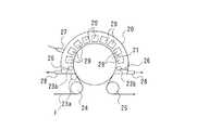
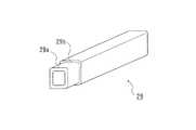
図3は、上述の円筒型のロール電極21の一例を示す概略図、図4は、円筒型の固定電極22の一例を示す概略図、図5は、角柱型の固定電極29の一例を示す概略図である。
【0052】
図3において、アース電極であるロール電極21は、金属等の導電性母材21aに対し、誘電体被覆層として、セラミックスを溶射後、無機化合物の封孔材料を用いて封孔処理したセラミックス被覆処理誘電体21bを被覆した組み合わせで構成されているものである。膜厚1mmのセラミックス被覆処理誘電体21bをロール電極21の外側に被覆し、アースに接地してある。また、溶射に用いるセラミックス材としては、アルミナ・窒化珪素等が好ましく用いられるが、この中でもアルミナが加工し易いので、更に好ましく用いられる。
【0053】
金属等の導電性母材21aとしては、チタン、銀、白金、ステンレス、アルミニウム、鉄等の金属等や、鉄とセラミックスとの複合材料又はアルミニウムとセラミックスとの複合材料が挙げられるが、加工の観点からはステンレスが好ましい。
なお、本実施の形態においては、ロール電極の母材は、冷却水による冷却手段を有するステンレス製ジャケットロール母材を使用している(不図示)。
【0054】
図4及び図5は、印加電極である固定の電極22、電極29であり、上記記載のロール電極21と同様な組み合わせで構成されている。すなわち、導電性母材としての中空のステンレスパイプ22a、29aに対し、上記同様の誘電体22b、29bを被覆し、放電中は冷却水による冷却が行えるようになっている。
【0055】
印加電極に電圧を印加する電源としては、特に限定はないが、パール工業製高周波電源(200kHz)、パール工業製高周波電源(800kHz)、日本電子製高周波電源(13.56MHz)、パール工業製高周波電源(150MHz)等が使用できる。
【0056】
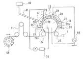
図6は、本発明に用いられるプラズマ放電処理装置10の一例を示す概念図である。
図6において、プラズマ放電処理容器20の部分は図2の記載と同様であるが、更に、ガス発生装置40、電源50、電極冷却ユニット70等が装置構成として配置されている。電極冷却ユニット70の冷却剤としては、蒸留水、油等の絶縁性材料が用いられる。
【0057】
図6に記載の電極21、29は、図3、4、5等に示したものと同様であり、対向する電極間のギャップは、例えば1mm程度に設定される。
上記電極間の距離は、電極の導電性母材に設けた固体誘電体の厚さ、印加電圧の大きさ、プラズマを利用する目的等を考慮して決定される。上記電極の一方に固体誘電体を設けた場合の固体誘電体と電極の最短距離、上記電極の双方に固体誘電体を設けた場合の固体誘電体同士の距離としては、いずれの場合も均一な放電を行う観点から0.5mm〜20mmが好ましく、特に好ましくは1mm±0.5mmである。
【0058】
前記プラズマ放電処理容器20内にロール電極21、固定電極29を所定位置に配置し、ガス供給手段としてのガス発生装置40で発生させた混合ガスを流量制御して、ガス充填手段41を介して給気口27よりプラズマ放電処理容器20内に入れ、前記プラズマ放電処理容器20内をプラズマ処理に用いる混合ガスで充填し排気口28より排気する。次に電源50により電極21、29に電圧を印加し、ロール電極21はアースに接地し、放電プラズマを発生させる。ここでロール状の元巻き基材60より基材Fを供給し、ガイドローラ24を介して、プラズマ放電処理容器20内の電極間を片面接触(ロール電極21に接触している)の状態で搬送され、基材Fは搬送中に放電プラズマにより表面が製膜され(CVD)、その後にガイドローラ25を介して、次工程に搬送される。ここで、基材Fはロール電極21に接触していない面のみ製膜がなされる。
【0059】
電源50より固定されている電極29に印加される電圧の値は適宜決定されるが、例えば、電圧が10V〜10kV程度で、電源周波数は100kHzを越えて150MHz以下に調整される。ここで電源の印加法に関しては、連続モードと呼ばれる連続サイン波状の連続発振モードとパルスモードと呼ばれるON/OFFを断続的に行う断続発振モードのどちらを採用しても良いが連続モードの方がより緻密で良質な膜が得られる。
【0060】
プラズマ放電処理容器20はパイレックス(R)ガラス製の処理容器等が好ましく用いられるが、電極との絶縁がとれれば金属製を用いることも可能である。例えば、アルミニウム又はステンレスのフレームの内面にポリイミド樹脂等を張り付けても良く、該金属フレームにセラミックス溶射を行い絶縁性をとっても良い。
【0061】
また、基材が樹脂製である場合、放電プラズマ処理時の基材への影響を最小限に抑制するために、放電プラズマ処理時の基材の温度を常温(15℃〜25℃)〜200℃未満の温度に調整することが好ましく、更に好ましくは常温〜100℃に調整することである。上記の温度範囲に調整する為、必要に応じて電極、基材は冷却手段で冷却しながら放電プラズマ処理される。
【0062】
本発明においては、上記の放電プラズマ処理が大気圧又は大気圧近傍で行われるが、ここで大気圧近傍とは、20kPa〜110kPaの圧力を表すが、本発明に記載の効果を好ましく得るためには、93kPa〜104kPaが好ましい。
【0063】
また、本発明の誘電体被覆電極においては、電極の少なくとも基材と接する側のJIS B 0601で規定される表面粗さの最大高さ(Rmax)が10μm以下になるように調整されることが、本発明に記載の効果を得る観点から好ましいが、更に好ましくは、表面粗さの最大値が8μm以下であり、特に好ましくは、7μm以下に調整することであり、このような範囲のRmaxとするためには、表面を研磨処理することが好ましい。
また、JIS B 0601で規定される中心線平均表面粗さ(Ra)は0.5μm以下が好ましく、更に好ましくは0.1μm以下である。
【0064】
なお、上述した図1〜図6に示すプラズマ放電処理装置10は、基材Fがフィルム等のように曲げられることのできる場合に使用される装置であったが、ある程度厚みのある基材Lまたは硬い基材L、例えばガラスやレンズ等であれば、図7に示すようなプラズマ放電処理装置100を使用する。図7は、プラズマ放電処理装置の他の例を示す概略図である。
【0065】
プラズマ放電処理装置(薄膜形成装置)100は、電源110、電極120等から概略構成されており、電極120は、上側平板電極121と下側平板電極122とを備えており、上側平板電極121と下側平板電極122とは上下に対向して配置されている。
上側平板電極121は、複数の略矩形状の平板電極121a,…が左右に対向して配置されて構成されたもので、これら複数の電極121a,…間の隙間がそれぞれガス流路部123,…とされている。つまり、上側平板電極121の上方には、ガス供給手段としてのガス供給部124が設けられており、このガス供給部124から反応性ガスや放電ガスがそれぞれのガス流路部123,…内に送給されて、下側平板電極122との間で噴出される。
下側平板電極122は、アースに接地してあり、基材Lをその表面に装着し、かつ、基材Lをガス流路部123に対して前後方向に往復移動させる。したがって、この下側平板電極122が移動することによって、上側平板電極121と下側平板電極122との間でプラズマ状態とされ、基材Lに製膜が行われる。
【0066】
次に、本発明のプラズマ放電処理装置に用いられるガスについて説明する。
本発明において使用するガスは、基材上に設けたい薄膜の種類によって異なるが、基本的に、放電ガスと、薄膜を形成するための反応性ガスである。反応性ガスは、放電空間に供給される全ガス量に対し、0.01〜10体積%含有させることが好ましい。薄膜の膜厚としては、0.1nm〜1000nmの範囲の薄膜が得られる。
【0067】
上記放電ガスとは、周期表の第18属元素、具体的には、ヘリウム、ネオン、アルゴン、クリプトン、キセノン、ラドン、窒素等が挙げられるが、ヘリウム、アルゴン又は窒素が好ましく用いられる。放電ガスは、放電ガスと反応性ガスの総量100体積%に対し、90体積%以上含有されることが好ましい。さらに好ましくは95体積%以上である。
【0068】
反応性ガスは、放電空間でプラズマ状態となり、薄膜を形成する成分を含有するものであり、有機金属化合物、有機化合物、無機化合物等である。
例えば、反応性ガスとして、ジンクアセチルアセトナート、トリエチルインジウム、トリメチルインジウム、ジエチル亜鉛、ジメチル亜鉛、エトラエチル錫、エトラメチル錫、二酢酸ジ−n−ブチル錫、テトラブチル錫、テトラオクチル錫などから選択された少なくとも1つの有機金属化合物を含むガスを用いて、導電性膜あるいは帯電防止膜、あるいは反射防止膜の中屈折率層として有用な金属酸化物層を形成することができる。
【0069】
また、反応性ガスとして、フッ素含有化合物ガスを用いることによって、基材表面にフッ素含有基を形成させて表面エネルギーを低くし、撥水性表面を得る撥水膜を得ることができる。フッ素元素含有化合物としては、6フッ化プロピレン(CF3CFCF2)、8フッ化シクロブタン(C4F8)等のフッ素・炭素化合物が挙げられる。安全上の観点から、有害ガスであるフッ化水素を生成しない6フッ化プロピレン、8フッ化シクロブタンを用いることができる。
【0070】
また、分子内に親水性基と重合性不飽和結合を有するモノマーの雰囲気下で処理を行うことにより、親水性の重合膜を堆積させることもできる。上記親水性基としては、水酸基、スルホン酸基、スルホン酸塩基、1級若しくは2級又は3級アミノ基、アミド基、4級アンモニウム塩基、カルボン酸基、カルボン酸塩基等の親水性基等が挙げられる。又、ポリエチレングリコール鎖を有するモノマーを用いても同様に親水性重合膜を堆積が可能である。
【0071】
上記モノマーとしては、アクリル酸、メタクリル酸、アクリルアミド、メタクリルアミド、N,N−ジメチルアクリルアミド、アクリル酸ナトリウム、メタクリル酸ナトリウム、アクリル酸カリウム、メタクリル酸カリウム、スチレンスルホン酸ナトリウム、アリルアルコール、アリルアミン、ポリエチレングリコールジメタクリル酸エステル、ポリエチレングリコールジアクリル酸エステルなどが挙げられ、これらの少なくとも1種が使用できる。
また、有機フッ素化合物、珪素化合物又はチタン化合物を含有する反応性ガスを用いることにより、反射防止膜の低屈折率層又は高屈折率層を設けることができる。
【0072】
有機フッ素化合物としては、フッ化炭素ガス、フッ化炭化水素ガス等が好ましく用いられる。フッ化炭素ガスとしては、4フッ化炭素、6フッ化炭素、具体的には、4フッ化メタン、4フッ化エチレン、6フッ化プロピレン、8フッ化シクロブタン等が挙げられる。前記のフッ化炭化水素ガスとしては、2フッ化メタン、4フッ化エタン、4フッ化プロピレン、3フッ化プロピレン等が挙げられる。
更に、1塩化3フッ化メタン、1塩化2フッ化メタン、2塩化4フッ化シクロブタン等のフッ化炭化水素化合物のハロゲン化物やアルコール、酸、ケトン等の有機化合物のフッ素置換体を用いることができるがこれらに限定されない。また、これらの化合物が分子内にエチレン性不飽和基を有していても良い。前記の化合物は単独でも混合して用いても良い。
【0073】
混合ガス中に上記記載の有機フッ素化合物を用いる場合、放電プラズマ処理により基材上に均一な薄膜を形成する観点から、混合ガス中の有機フッ素化合物の含有率は、0.1〜10体積%であることが好ましいが、更に好ましくは、0.1〜5体積%である。
【0074】
また、有機フッ素化合物が常温、常圧で気体である場合は、混合ガスの構成成分として、そのまま使用できる。しかし、有機フッ素化合物が常温・常圧で液体又は固体である場合には、加熱、減圧等の方法により気化して使用すればよく、また、又、適切な溶剤に溶解して用いてもよい。
【0075】
混合ガス中に上記記載のチタン化合物を用いる場合、放電プラズマ処理により基材上に均一な薄膜を形成する観点から、混合ガス中のチタン化合物の含有率は、0.01〜10体積%であることが好ましいが、更に好ましくは、0.01〜5体積%である。
【0076】
また、反応性ガスとして、水素化金属化合物、ハロゲン化金属化合物、水酸化金属化合物、過酸化金属化合物などを用いることも可能であり、これらを適宜気化して用いればよい。
【0077】
また、上記記載の混合ガス中に水素ガスを0.1〜10体積%含有させることにより薄膜の硬度を著しく向上させることができる。
また、混合ガス中に酸素、オゾン、過酸化水素、二酸化炭素、一酸化炭素、水素、窒素から選択される成分を0.01〜5体積%含有させることにより、反応促進され、且つ、緻密で良質な薄膜を形成することができる。
上記記載の珪素化合物、チタン化合物としては、取り扱い上の観点から金属水素化合物、金属アルコキシドが好ましく、腐食性、有害ガスの発生がなく、工程上の汚れなども少ないことから、金属アルコキシドが好ましく用いられる。
【0078】
また、上記記載の珪素化合物、チタン化合物を放電空間である電極間に導入するには、両者は常温常圧で、気体、液体、固体いずれの状態であっても構わない。気体の場合は、そのまま放電空間に導入できるが、液体、固体の場合は、加熱、減圧、超音波照射等の手段により気化させて使用される。珪素化合物、チタン化合物を加熱により気化して用いる場合、テトラエトキシシラン、テトライソプロポキシチタンなど、常温で液体で、沸点が200℃以下である金属アルコキシドが反射防止膜の形成に好適に用いられる。上記金属アルコキシドは、溶媒によって希釈して使用されても良く、溶媒は、メタノール、エタノール、n−ヘキサンなどの有機溶媒及びこれらの混合溶媒が使用できる。なお、これらの希釈溶媒は、プラズマ放電処理中において、分子状、原子状に分解される為、基材上への薄膜の形成、薄膜の組成などに対する影響は殆ど無視することができる。
【0079】
上記記載の珪素化合物としては、例えば、ジメチルシラン、テトラメチルシランなどの有機金属化合物、モノシラン、ジシランなどの金属水素化合物、二塩化シラン、三塩化シランなどの金属ハロゲン化合物、テトラメトキシシラン、テトラエトキシシラン、ジメチルジエトキシシランなどのアルコキシシラン、オルガノシランなどを用いることが好ましいがこれらに限定されない。また、これらは適宜組み合わせて用いることができる。
【0080】
ガス中に上記記載の珪素化合物を用いる場合、放電プラズマ処理により基材上に均一な薄膜を形成する観点から、混合ガス中の珪素化合物の含有率は、0.1〜10体積%であることが好ましいが、更に好ましくは、0.1〜5体積%である。
【0081】
上記記載のチタン化合物としては、テトラジメチルアミノチタンなどの有機金属化合物、モノチタン、ジチタンなどの金属水素化合物、二塩化チタン、三塩化チタン、四塩化チタンなどの金属ハロゲン化合物、テトラエトキシチタン、テトライソプロポキシチタン、テトラブトキシチタンなどの金属アルコキシドなどを用いることが好ましいがこれらに限定されない。
【0082】
反応性ガスに有機金属化合物を添加する場合、例えば、有機金属化合物としてLi,Be,B,Na,Mg,Al,Si,K,Ca,Sc,Ti,V,Cr,Mn,Fe,Co,Ni,Cu,Zn,Ga,Ge,Rb,Sr,Y,Zr,Nb,Mo,Cd,In,Ir,Sn,Sb,Cs,Ba,La,Hf,Ta,W,Tl,Pb,Bi,Ce,Pr,Nd,Pm,Eu,Gd,Tb,Dy,Ho,Er,Tm,Yb,Luから選択される金属を含むことができる。より好ましくは、これらの有機金属化合物が金属アルコキシド、アルキル化金属、金属錯体から選ばれるものが好ましい。
【0083】
上記又は上記以外の反応性ガスを適宜選択して使用することにより、様々な高機能性の薄膜を得ることができる。その一例を以下に示すが、本発明はこれに限られるものではない。
電極膜 Au,Al,Ag,Ti,Pt,Mo,Mo−Si
誘電体保護膜 SiO2,SiO,Si3N4,Al2O3,Y2O3
透明導電膜 In2O3,SnO2
エレクトロクロミック膜 WO3,IrO2,MoO3,V2O5
蛍光膜 ZnS,ZnS+ZnSe,ZnS+CdS
磁気記録膜 Fe−Ni,Fe−Si−Al,γ−Fe2O3,Co,Fe3O4、Cr,SiO2,AlO3
超導電膜 Nb,Nb−Ge,NbN
太陽電池膜 a−Si,Si
反射膜 Ag,Al,Au,Cu
選択性吸収膜 ZrC−Zr
選択性透過膜 In2O3,SnO2
反射防止膜 SiO2,TiO2,SnO2
シャドーマスク Cr
耐摩耗性膜 Cr,Ta,Pt,TiC,TiN
耐食性膜 Al,Zn,Cd,Ta,Ti,Cr
耐熱膜 W,Ta,Ti
潤滑膜 MoS2
装飾膜 Cr,Al,Ag,Au,TiC,Cu
【0084】
次に、本発明に用いることのできる基材について説明する。
本発明に用いることができる基材としては、フィルム状のもの、レンズ状等の立体形状のもの等、薄膜をその表面に形成できるものであれば特に限定はない。基材が電極間に載置できるものであれば、電極間に載置することによって、基材が電極間に載置できないものであれば、発生したプラズマを当該基材に吹き付けることによって薄膜を形成すればよい。
【0085】
基材を構成する材料も特に限定はないが、大気圧又は大気圧近傍の圧力下であることと、低温のグロー放電であることから、樹脂を好ましく用いることができる。
基材として好ましくはフィルム状のセルローストリアセテート等のセルロースエステル、ポリエステル、ポリカーボネート、ポリスチレン、更にこれらの上にゼラチン、ポリビニルアルコール(PVA)、アクリル樹脂、ポリエステル樹脂、セルロース系樹脂等を塗設したもの等を使用することができる。
【0086】
上記基材としては、具体的には、ポリエチレンテレフタレート、ポリエチレンナフタレート等のポリエステルフィルム、ポリエチレンフィルム、ポリプロピレンフィルム、セロファン、セルロースジアセテートフィルム、セルロースアセテートブチレートフィルム、セルロースアセテートプロピオネートフィルム、セルロースアセテートフタレートフィルム、セルローストリアセテート、セルロースナイトレート等のセルロースエステル類又はそれらの誘導体からなるフィルム、ポリ塩化ビニリデンフィルム、ポリビニルアルコールフィルム、エチレンビニルアルコールフィルム、シンジオタクティックポリスチレン系フィルム、ポリカーボネートフィルム、ノルボルネン樹脂系フィルム、ポリメチルペンテンフィルム、ポリエーテルケトンフィルム、ポリイミドフィルム、ポリエーテルスルホンフィルム、ポリスルホン系フィルム、ポリエーテルケトンイミドフィルム、ポリアミドフィルム、フッ素樹脂フィルム、ナイロンフィルム、ポリメチルメタクリレートフィルム、アクリルフィルムあるいはポリアリレート系フィルム等を挙げることができる。
【0087】
これらの素材は単独で、あるいは適宜混合されて使用することもできる。中でも、セルローストリアセテート(TAC)が好ましく用いられる。また、特開平3−14882号や特開平3−122137号などで公知のノルボルネン系樹脂(非晶質シクロポリオレフィン樹脂)を含有したゼオノア(日本ゼオン(株)製)、ARTON(JSR(株)製)などの市販品を好ましく使用することができる。ノルボルネン系樹脂は、具体的にはノルボルネン系単量体の開環重合体、その水素添加物、ノルボルネン系単量体の付加型重合体、ノルボルネン系単量体(上記公報、特開平2−227424号、特開平2−276842号に記載)とオレフィンの付加型重合体などが挙げられる。ノルボルネン系単量体の重合は公知の方法でよく、必要に応じて、水素添加することにより、熱可塑性ノルボルネン系樹脂水素添加物、具体的には上述したゼオノア、ARTON等を得ることができる。
【0088】
更に、ポリカーボネート、ポリアリレート、ポリスルフォン及びポリエーテルスルフォン(PES)(例えば、住友ベークライト(株)製 スミライト FS−1300)などの固有複屈折率の大きい素材であっても、溶液流延、溶融押し出し等の条件、更には縦、横方向に延伸条件等を適宜設定することにより、得ることができる。
【0089】
また、基材には、有機無機ハイブリッド基材を使用することもできる。有機無機ハイブリッド基材とは、水素結合受容基を有するポリマーあるいは重合性モノマーと、金属アルコキシド等の反応性金属化合物とを加水分解重縮合させて得られるものである。
ポリマーとしては、ポリビニルアルコール、ポリ酢酸ビニル、ポリビニルピロリドン、ポリイミド、ポリアミド、ポリカーボネイト、ポリ尿素、ポリエステル、ポリウレタン、ポリ(2−メチル−2−オキサゾリン)、ポリアクリルアミド、ポリ(N−イソプロピルアクリルアミド)、ポリ(ジメチルアクリルアミド)、ポリエーテルイミド、セルロースエステルなどが挙げられるが、この中ではセルロースエステルが好ましい。
重合ポリマーとしては、イソプレン、1,3−ブタジエン、p−シアノスチレン、p−メトキシスチレン、メタクリロニトリル、p−クロロスチレン、スチレン、α−メチルスチレン、メチルメタクリレート、メチルビニルケトン、アクリロニトリル、メチルアクリレート、酢酸ビニル、エチレン、イソブテン、塩化ビニリデン、塩化ビニル、イソブチルエーテル、ジメチルアクリルアミドなどが挙げられる。
前記金属アルコキシドとしては、金属種が、珪素、ジルコニウム、チタン、ゲルマニウム等のアルコキシドが挙げられるが、この中では珪素やチタンのアルコキシドが好ましい。
具体的な製法としては、特開2000−122038号公報を参考にして合成することが可能である。
【0090】
これらフィルムの膜厚としては10μm〜1000μmが好ましい。
【0091】
以上のようにして、プラズマ放電処理装置によって大気圧プラズマ処理を施すことで、基材上に薄膜を形成する。
【0092】
【実施例】
以下、本発明を実施例により具体的に説明するが、本発明はこれらに限定されない。
(本発明の実施例1:誘電体被覆電極セットAの作製)
上述の図2のプラズマ放電処理容器20を用いたプラズマ放電処理装置において、誘電体で被覆したロール電極及び複数の角柱型の印加電極のセットを以下のように作成した。
ロール電極21は、冷却水による冷却手段を有するステンレス製ジャケットロール母材(冷却手段は図2には図示していない)に対して、大気プラズマ法により高密度、高密着性のアルミナ溶射膜を被覆し、ロール径1000mmφとなるようにした。その後、テトラメトキシシランを酢酸エチルで希釈した溶液を塗布乾燥後、紫外線照射により硬化させ封孔処理を行った。
このようにして被覆した誘電体表面を研磨し、平滑にして、Rmax5μmとなるように加工した。
【0093】
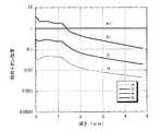
そして、作成した誘電体被覆電極に対して、ダイナミックSIMS測定によって誘電体被覆電極の深さ方向の分析(Si及びAlのイオン強度の測定)を行い、その結果を図8に示した。図8において、横軸は、誘電体被覆電極の最表面からの深さ(μm)を表し、縦軸は、誘電体に含有されている物質のイオン強度を表す。
本実施例におけるダイナミックSIMS測定の測定条件は、
一次イオン:O2+
加速電圧:5kV
一次イオン電流:300nA
一次イオン照射面積:300μm角
取り込みエリア:照射面積の9%
なお、Alの測定条件は、
Alの検出強度:Alイオンの検出強度が高く、検出器が飽和してしまうため、Alの検出強度が1/10となるようにFAP(Field Axis Potential)を調整する。この実施例中では、Alに対してのみFAP−offset=5Vとして測定する。
検出ピーク:Alについては27a.m.uを、Siについては30a.m.uを測定ピークとする。
検出ピークの極性:正イオンを測定
図8より、誘電体の最表面から深さ約1.38μmまではSiのイオン強度がAlのイオン強度よりも大きく、深さ約1.38μmから導電性母材の表面まではAlのイオン強度がSiのイオン強度よりも大きいことが確認された。
【0094】
また、作成した誘電体被覆電極において最終的な誘電体の空隙率は5体積%であり、このときの誘電体層のSiOx含有率は75モル%であった。最終的な誘電体の膜厚は、1mm(膜厚変動±1%以内)であった。また、誘電体の比誘電率は10であった。導電性母材と誘電体の線熱膨張係数の差は、9.8×10⁻⁶/℃であった。上述のごとくロール電極21を作成し、アース(接地)した。
【0095】
一方、印加電極としては、中空の角型の純チタンパイプに対し、上記同様の誘電体を同条件にて被覆し、対向する電極群とした。この印加電極の誘電体については上記ロール電極のものと物性は同じであるが、導電性母材と誘電体の線熱膨張差は1.7×10⁻⁶/℃であった。この印加電極の放電総面積は、150cm(幅手方向の長さ)×2cm(搬送方向の長さ)×50本(印加電極の数)=15000cm2であった。
このようにして作成した対向する電極セットAの耐熱温度は、200℃、耐電圧は10kV以上、限界出力は400kW/m2以上であり、240時間連続放電でも全く破壊は認められなかった。
【0096】
(本発明の実施例2:誘電体被覆電極セットBの作製)
上述の本発明の誘電体被覆電極セットAにおいて、印加電極に用いた中空の角型の純チタンパイプを、ステンレスパイプに変更した以外は、同様にして誘電体被覆電極セットBを作成した。ステンレスに変更したことにより、印加電極の導電性母材と誘電体の線熱膨張係数の差は、9.8×10⁻⁶/℃となった以外は、誘電体表面のRmax、Si及びAlのイオン強度、SiOx含有量、誘電体膜厚及び比誘電率は誘電体被覆電極セットAと同様であった。
このようにして得られた誘電体被覆電極セットBの耐熱温度は120℃、耐電圧は10kV以上、限界出力は400kW/m2以上であり、240時間連続放電でも全く破壊は認められなかった。
【0097】
(比較例:誘電体被覆電極セットの作製)
封孔処理を行わずに、上記本発明の誘電体被覆電極セットAと同様にして導電性母材に対して大気プラズマ法によりアルミナ溶射膜を被覆し、誘電体被覆電極セットを作成した。
このようにして得られた誘電体被覆電極セットの耐熱温度、耐電圧、限界出力は、当初は上述の本願実施例と同等の性能であったが、連続運転24時間でスパークを起こし、破壊してしまった。
【0098】
(本発明の実施例3:薄膜形成装置の作成と薄膜形成)
上記実施例1で作成した本発明の誘電体被覆電極セットAを、図6のプラズマ放電処理装置(薄膜形成装置)に設置した。また、電源は、日本電子製高周波電源(13.56MHz)を使用した。
長尺の樹脂フィルムを基材として、以下の条件で連続的に薄膜を形成したところ、屈折率2.3の高品質な酸化チタン膜が得られた。
放電条件:放電出力 1.2W/cm2
放電ガス:アルゴン 98.75体積%
反応性ガス1:水素ガス ガス全量に対して1体積%
反応性ガス2:テトライソプロポキシチタン蒸気(150℃に加熱した液体にアルゴンガスをバブリング)ガス全量に対して0.25体積%
以上、本発明の実施の形態及び実施例について説明したが、本発明は、係る実施の形態又は実施例に限定されず、その要旨を逸脱しない範囲で種々の変形が可能であることはいうまでもない。
例えば、本発明の実施の形態及び実施例では、基板の表面に薄膜を形成することにプラズマ放電処理装置を用いたが、本発明はこれに限らず、基板の種々の表面処理等にも適用可能である。
【0099】
【発明の効果】
本発明によれば、ダイナミックSIMS測定による第1の金属原子のイオン強度及び第2の金属原子のイオン強度が、誘電体の最表面から所定の深さまでは、第2の金属原子のイオン強度が大きく、前記所定の深さから導電性母材の表面までは、第1の金属原子のイオン強度が大きいので、第2の金属原子によって誘電体の最表面の空隙が埋められて、対向する電極間に大電力(100kHzを越える高周波電圧、1W/cm2以上の電力)を供給した場合でも絶縁破壊を防止することができ、安定な放電状態を長時間維持することが可能となる。
【図面の簡単な説明】
【図1】本発明のプラズマ放電処理装置(薄膜形成装置)に設置されるプラズマ放電処理容器の一例を示す概略図である。
【図2】プラズマ放電処理容器の他の一例を示す概略図である。
【図3】円筒型のロール電極の一例を示す斜視図である。
【図4】固定型の円筒型電極の一例を示す斜視図である。
【図5】固定型の角柱型電極の一例を示す斜視図である。
【図6】プラズマ放電処理装置の一例を示す概略図である。
【図7】プラズマ放電処理装置の他の一例を示す概略図である。
【図8】本発明の実施例1における誘電体のダイナミックSIMS測定による深さ方向における第1の金属原子と第2の金属原子とのイオン強度比の分析結果を示すグラフである。
【符号の説明】
F フィルム(基材)
L レンズ(基材)
10、100 プラズマ放電処理装置
21、22 電極(ロール電極)
29 電極(固定電極)
50、110 電源
120 電極
121 上側平板電極
122 下側平板電極[0001]
BACKGROUND OF THE INVENTION
The present invention relates to a dielectric coated electrode in which a surface of a conductive base material is coated with a dielectric, a plasma discharge processing apparatus provided with the dielectric coated electrode, and a thin film forming method using the dielectric coated electrode.
[0002]
[Prior art]
In recent years, various high-functional films such as a conductive film, an antireflection film, and an antistatic film have been used in liquid crystal display elements, semiconductor elements, optical elements, and the like. As a method for forming these high-performance films, a method of forming a thin film on the surface of a substrate or the like that is discharged under atmospheric pressure or near atmospheric pressure, plasma-excited reactive gas, and disposed between electrodes (atmospheric pressure) Plasma method) is described in JP-A-11-133205, JP-A-2000-185362, JP-A-11-61406, JP-A-2000-147209, 2000-121804, and the like.
In the atmospheric pressure plasma method disclosed in these publications, a voltage having a frequency of 0.5 to 100 kHz is applied between opposing electrodes so that an electric field strength is 1 to 100 V / cm, and discharge plasma is applied. It is to generate.
[0003]
[Problems to be solved by the invention]
By the way, an electrode used in such an atmospheric pressure plasma method needs to cover the electrode surface with a dielectric in order to obtain a stable glow discharge under atmospheric pressure. The dielectric is not particularly limited as long as it has a desired dielectric constant. Generally, rubber, ceramic, glass, and the like are known.
In Japanese Patent Application Laid-Open No. 11-191500, the present applicant has proposed a technique in which a dielectric coated electrode obtained by spraying ceramic alumina on a metal base material is used in an atmospheric pressure plasma processing apparatus. Such dielectric-covered electrodes are more durable than electrodes made solely of rubber or glass, change the surface properties such as wettability and adhesiveness of the substrate surface, and remove contamination on the substrate surface. There is no problem at all in so-called surface treatment.
However, when the present inventor has studied the case where a high-performance thin film is formed in a large area by the atmospheric pressure plasma method, it is necessary to apply a high-frequency voltage having a higher frequency and a higher power than the surface treatment. It has been found that the above-mentioned dielectric-coated electrode, which is just sprayed with alumina, has insufficient durability. Specifically, the frequency exceeds 100 kHz between the dielectric coating electrodes facing each other in the atmospheric pressure plasma processing apparatus, and the power is 1 W / cm.2This is a finding that it is necessary to apply the above high-frequency voltage. Therefore, as a result of earnest research on high durability electrodes that can withstand the application of such high power voltage, even if a high power voltage is applied, the discharge is stable for a long time by controlling the composition near the surface of the dielectric. We have found a dielectric coated electrode that can maintain its state.
[0004]
The present invention relates to a dielectric coated electrode capable of maintaining a stable discharge state for a long time even when high power is applied, a plasma discharge processing apparatus provided with the dielectric coated electrode, and a thin film forming method using the dielectric coated electrode It is an issue to provide.
[0005]
[Means for Solving the Problems]
In order to solve the above problems, the invention of claim 1In the thin film formation method, a step of supplying a reactive gas between opposing electrodes, and discharging by applying a high-frequency voltage with a total power exceeding 15 kW between the opposing electrodes under atmospheric pressure or near atmospheric pressure. A step of bringing the reactive gas into a plasma state, supplying a base material between the opposing electrodes, and exposing the base material to the reactive gas in the plasma state to form a thin film on the surface of the base material Forming at least one of the opposing electrodes,
A dielectric-coated electrode in which a surface of a conductive base material is coated with a dielectric,
The dielectric contains a first metal atom and a second metal atom,
The ionic strength of the first metal atom and the ionic strength of the second metal atom by dynamic SIMS measurement are such that the ionic strength of the second metal atom is a predetermined depth from the outermost surface of the dielectric. The ionic strength of the first metal atom is greater than the ionic strength of the second metal atom from the predetermined depth to the surface of the conductive base material.The
A dielectric-coated electrode having a dielectric thickness of 0.5 to 2 mm and a film thickness variation of 5% or less, and a difference in coefficient of linear thermal expansion between the dielectric and the conductive base material is 2 × 10⁻⁶/ ℃ or lessIt is characterized by that.
According to a second aspect of the present invention, in the thin film formation method, a reactive gas is supplied between the opposing electrodes, and the total electric power exceeding 15 kW between the opposing electrodes under atmospheric pressure or pressure near atmospheric pressure. By applying a high frequency voltage to discharge, the reactive gas is brought into a plasma state, and a base material is supplied between the opposing electrodes, and the base material is exposed to the reactive gas in the plasma state. Forming a thin film on the surface of the base material, and the opposing electrode comprises:
A dielectric-coated electrode in which a surface of a conductive base material is coated with a dielectric,
The dielectric contains a first metal atom and a second metal atom,
The ionic strength of the first metal atom and the ionic strength of the second metal atom by dynamic SIMS measurement are such that the ionic strength of the second metal atom is a predetermined depth from the outermost surface of the dielectric. From the predetermined depth to the surface of the conductive base material, the ionic strength of the first metal atom is greater than the ionic strength of the second metal atom,
A dielectric-coated electrode having a dielectric thickness of 0.5 to 2 mm and a film thickness variation of 5% or less, and a difference in coefficient of linear thermal expansion between the dielectric and the conductive base material is 2 × 10⁻⁶/ ° C. or less.
[0006]
The invention of
The predetermined depth is 1 μm or more.
[0007]
Invention of Claim 4 is described in Claim 3.Thin film formation methodIn
The ionic strength of the second metal atom relative to the ionic strength of the first metal atom is reduced from the outermost surface of the dielectric to the predetermined depth.
[0008]
Invention of
The first metal atom is Al, and the second metal atom is Si.
[0009]
Invention of Claim 6 is as described in any one of Claims 3-5.Thin film formation methodIn
The dielectric-coated electrode is obtained by thermally spraying a material containing the first metal atom on the conductive base material, and then sealing the material with the material containing the second metal atom. And
[0010]
The invention according to claim 7 is the invention according to claim 6.Thin film formation methodIn
The material containing the first metal atom is alumina.
[0011]
The invention according to claim 8 is the invention according to claim 6 or 7.Thin film formation methodIn
The sealing treatment is characterized in that the material containing the second metal atom is applied to the surface of the electrode after the thermal spraying and is cured by a sol-gel reaction.
[0012]
The invention according to claim 9 is the invention according to claim 8.Thin film formation methodIn
The hardened material containing the second metal atom is silicon oxide.
[0013]
Invention of
The dielectric has a porosity of 10% by volume or less.
[0015]
Invention of Claim 11 is as described in any one of Claims 3-10.Thin film formation methodIn
The heat resistant temperature is 100 ° C. or higher.
[0020]
DETAILED DESCRIPTION OF THE INVENTION
Embodiments of the present invention will be described below.
The dielectric-coated electrode of the present invention is formed by spraying a material mainly composed of a first metal atom on the surface of a conductive base material such as metal to coat the dielectric, and then applying the second surface layer of the dielectric to the second layer. It is preferable that it is what was sealed with the sealing agent which has a metal atom as a main component.
[0021]
In this case, the ionic strength of the first metal atom and the ionic strength of the second metal atom by dynamic SIMS measurement are such that the ionic strength of the second metal atom is the first metal at a predetermined depth from the outermost surface of the dielectric. The ionic strength of the first metal atom is greater than the ionic strength of the second metal atom from the predetermined depth to the surface of the conductive base material.
[0022]
Moreover, it is preferable that the ionic strength of the second metal atom corresponding to the ionic strength of the first metal atom decreases from the outermost surface of the dielectric to the predetermined depth. Decreasing means that the ion concentration is lower at the predetermined depth than the outermost surface of the dielectric.
It is preferable that the concentration curve from the outermost surface to the predetermined depth is continuous. This only eliminates the case where the layer mainly composed of the first metal atom and the layer mainly composed of the second metal atom are present separately (discontinuous). . The density change rate may be monotonously decreased with a constant density change rate, or the density change rate may not be constant but continuously negative.
This is because the electrode material of the present invention is formed by soaking the material containing the second metal atom from the surface of the sprayed film of the material containing the first metal atom on the electrode base material. is doing. Although details are unknown, it is estimated that the durability of the entire electrode is improved by controlling the composition from the outermost surface of the dielectric.
The predetermined depth is preferably 1 μm or more.
[0023]
As described above, the ionic strength of the second metal atom is increased at a predetermined depth from the outermost surface of the dielectric, and the ionic strength of the first metal atom is increased from the predetermined depth to the surface of the conductive base material. By doing so, it is presumed that the void formed on the outermost surface of the dielectric is filled with the second metal atoms to form a dense film.
On the other hand, in the vicinity of the surface of the base material, there is not much penetration of the second metal atoms, and there is an appropriate gap, so that it is considered that the expansion difference between the base material and the dielectric due to the temperature rise can be absorbed. Therefore, for example, a high frequency voltage exceeding 100 kHz and 1 W / cm2When the above high power is supplied between the electrodes facing each other, dielectric breakdown usually occurs from the surface of the electrode, but as described above, the ionic strength of the second metal atom is increased to a predetermined depth and the dense film Thus, dielectric breakdown can be prevented. Therefore, the discharge state can be maintained for a long time.
[0024]
Here, dynamic secondary ion mass spectrometry (Dynamic Secondary Ion Mass Spectrometry) means that O on the sample surface.2, Cs, Ar, Xe, and other ions are irradiated to detect secondary ions emitted from the surface. Since this method is a method in which measurement is performed while continuously irradiating ions and scraping the sample, the distribution state in the depth direction can be analyzed. In Examples described later, ADEPT-1010 manufactured by Physical Electronics, USA was used.
In this dynamic SIMS measurement, the detection intensity of the metal ion of the first metal atom is high and the detector may be saturated, so FAP (Field Axis Potential) is used to weaken the detection intensity of the metal ion. Adjust and measure. In addition, when the detection intensity of the metal ion of the second metal atom is high and the detector or the like may be saturated, the measurement is performed by adjusting the FAP so as to reduce the detection intensity of the metal ion. Good.
[0025]
The dielectric-coated electrode of the present invention is one in which at least a discharge surface on a conductive base material is coated with a dielectric. That is, when a thin film forming apparatus (plasma discharge processing apparatus) described later is provided, at least one of the facing application electrode and the ground electrode is covered with a dielectric, preferably both the application electrode and the ground electrode. Covering the dielectric.
[0026]
Specifically, the dielectric used for the dielectric-coated electrode of the present invention, that is, the material containing the first metal atom, is preferably an inorganic compound having a relative dielectric constant of 6 to 45, Examples of such a dielectric include ceramics such as alumina and silicon nitride. Among these, a ceramic sprayed one is preferable. In particular, a sprayed alumina is preferable.
[0027]
An example of a method for thermally spraying the conductive base material with high density and high adhesion using ceramic as a dielectric material is an atmospheric plasma spraying method. The atmospheric plasma spraying technique is a technique in which fine powder such as ceramics, wire, or the like is put into a plasma heat source and sprayed onto a conductive base material to be coated as fine particles in a molten or semi-molten state to form a film.
[0028]
A plasma heat source is a high-temperature plasma gas in which a molecular gas is heated to a high temperature, dissociated into atoms, and energy is given to emit electrons. The plasma gas injection speed is high, and since the sprayed material collides with the conductive base material at a higher speed than conventional arc spraying or flame spraying, it is possible to obtain a coating film with high adhesion strength and high density.
Specifically, reference can be made to a thermal spraying method for forming a heat shielding film on a high-temperature exposed member described in JP-A No. 2000-301655. According to this method, the porosity of the dielectric (ceramic sprayed film) to be coated can be 10% by volume or less, and further 8% by volume or less.
[0029]
The sealing treatment performed on the surface of the thermal spray film (dielectric) such as ceramic coated as described above is preferably performed with a material containing the second metal atom, that is, an inorganic compound. As the inorganic compound, metal oxides are preferable, and among them, those containing silicon oxide (SiOx) as a main component are particularly preferable. By performing the sealing treatment, the porosity of the dielectric can be further reduced.
[0030]
Moreover, it is preferable that the inorganic compound for sealing treatment is formed by curing by a sol-gel reaction. In the case where the inorganic compound for sealing treatment contains a metal oxide as a main component, a metal alkoxide or the like is applied as a sealing liquid on the ceramic sprayed film and cured by a sol-gel reaction. When the inorganic compound is mainly composed of silica, it is preferable to use alkoxysilane as the sealing liquid.
[0031]
Here, it is preferable to use energy treatment for promoting the sol-gel reaction. Examples of the energy treatment include thermosetting (preferably 200 ° C. or less), UV irradiation, and the like. Furthermore, as a method of sealing treatment, when the sealing liquid is diluted and coating and curing are repeated several times in succession, the mineralization is further improved and a dense electrode without deterioration can be obtained.
[0032]
In the case of performing a sealing treatment that cures by a sol-gel reaction after coating a ceramic sprayed film with the metal alkoxide or the like of the dielectric-coated electrode of the present invention as a sealing liquid, the content of the metal oxide after curing is 60 mol. % Or more is preferable. When alkoxysilane is used as the metal alkoxide of the sealing liquid, the cured SiOx content (x is 2 or less) is preferably 60 mol% or more. The SiOx content after curing is measured by analyzing a fault of the dielectric layer by XPS.
[0033]
In the dielectric-coated electrode, as one of the specifications that can withstand the high power as described above, as a result of intensive studies by the present inventors, the porosity of the dielectric is 10% by volume or less, preferably 8% by volume or less. I found. Preferably it is more than 0 volume% and 5 volume% or less. The porosity of the dielectric means a porosity that is penetrable in the thickness direction of the dielectric, and can be measured with a mercury porosimeter. In the examples described later, the porosity of the dielectric covered with the conductive base material was measured with a mercury porosimeter manufactured by Shimadzu Corporation.
[0034]
High durability is achieved because the dielectric has a low porosity. Examples of the dielectric having such a void and having a low void ratio include a high-density, high-adhesion ceramic spray coating by the atmospheric plasma method described later.
[0035]
In addition, in the dielectric-coated electrode of the present invention, another preferred specification that can withstand high power is that the heat-resistant temperature is 100 ° C. or higher. More preferably, it is 120 degreeC or more, Most preferably, it is 150 degreeC or more. The heat-resistant temperature refers to the temperature of the dielectric surface that can withstand normal discharge without breakdown, that is, the surface of the surface opposite to the conductive base material of the dielectric.
For such heat-resistant temperature, the dielectric provided by the above-mentioned ceramic spraying is applied, or a means for appropriately selecting a material within the range of the difference in linear thermal expansion coefficient between the conductive base material and the dielectric is appropriately combined. Is achievable.
[0036]
In the dielectric-coated electrode of the present invention, another preferred specification is that the difference in coefficient of linear thermal expansion between the dielectric and the conductive base material is 10 × 10.-6It is a combination that becomes / ° C or less. Preferably 8 × 10⁻⁶/ ° C. or less, more preferably 5 × 10⁻⁶/ ° C. or less, more preferably 2 × 10⁻⁶/ ° C or less. The linear thermal expansion coefficient is a well-known physical property value of a material.
In addition, the linear thermal expansion coefficient of the dielectric means the linear thermal expansion coefficient of the entire dielectric, and is obtained by removing the dielectric from the conductive base material and measuring the entire dielectric. equal.
[0037]
As a combination of a conductive base material and a dielectric whose linear thermal expansion coefficient is within this range,
(1) The conductive base material is pure titanium and the dielectric is ceramic.
(2) The conductive base material is a titanium alloy, and the dielectric is ceramic.
(3) The conductive base material is stainless steel, and the dielectric is ceramic.
(4) The conductive base material is a composite material of ceramics and iron, and the dielectric is ceramics.
(5) The conductive base material is a composite material of ceramics and aluminum, and the dielectric is ceramics.
Etc. From the viewpoint of the difference in linear thermal expansion coefficient, the above (1), (2), (4) and (5) are preferable.
[0038]
In the dielectric-coated electrode of the present invention, another preferred specification that can withstand high power is that the dielectric thickness is 0.5 to 2 mm. The film thickness variation is desirably 5% or less, preferably 3% or less, and more preferably 1% or less.
[0039]
Further, the surface roughness Rmax (JIS B 0601) of the electrode is reduced to 10 μm or less by a method such as polishing the dielectric surface of the dielectric coated electrode, so that the thickness of the dielectric and the gap between the electrodes are made constant. It can be maintained, the discharge state can be stabilized, distortion and cracking due to thermal shrinkage difference and residual stress can be eliminated, and durability can be greatly improved with high accuracy. The polishing finish of the dielectric surface is preferably performed at least on the dielectric in contact with the substrate.
[0040]
In addition, such dielectric-coated electrodes of the present invention are arranged to face each other, with a high frequency voltage exceeding 100 kHz between the opposed electrodes under a pressure of atmospheric pressure or near atmospheric pressure, and 1 W / cm.2A plasma discharge such as a thin film forming apparatus that forms a thin film on the surface of a substrate by supplying the above electric power and discharging the reactive gas into a plasma state and exposing the substrate to the reactive gas in a plasma state. It is preferable that the processing apparatus is provided.
[0041]
In the present invention, the upper limit of the frequency of the high-frequency voltage applied between the electrodes is preferably 150 MHz or less. Further, the lower limit value of the frequency of the high frequency voltage is preferably 200 kHz or more, and more preferably 800 kHz or more.
The lower limit value of the power supplied between the electrodes is preferably 1.2 W / cm.2The upper limit is preferably 50 W / cm.2Or less, more preferably 20 W / cm2It is as follows. The discharge area (/ cm2) Refers to the area of the area where discharge occurs in the electrode. When a high power voltage is applied at a high frequency and a high output density as in the present invention, this corresponds to the total area of the discharge surface of the electrode on one side. By dividing the total power (W) supplied from the power source connected to the electrode by this total area, the output density can be calculated.
[0042]
In order to obtain a uniform film thickness particularly in a large area, the total power applied to a pair of opposing electrodes is preferably more than 15 kW, more preferably 30 kW or more, and further preferably 50 kW or more. From the viewpoint of heat generation, it is preferably 300 kW or less. The total power corresponds to the power (W) supplied from the power source connected to the set of electrodes. When two or more power sources are connected to the set of electrodes, the value is a value obtained by adding the power supplied to all the power sources.
[0043]
Specifically, in the plasma discharge processing apparatus of FIG. 6 described later, the
[0044]
The high-frequency voltage applied between the electrodes may be an intermittent pulse wave or a continuous sine wave. However, in order to obtain the effect of the present invention, it is a continuous sine wave. It is preferable.
[0045]
By applying a high-power electric field as described above over a large area, it is possible to obtain a high-performance thin film that is dense, highly uniform in film thickness, and has no unevenness with high production efficiency. The inventors have found. The inventors presume that this excellent effect is due to the fact that high-density plasma can be generated uniformly over a large area by using the above high-power discharge method. Yes.
[0046]
Next, a plasma discharge processing apparatus using such an electrode will be described with reference to FIGS. The plasma discharge treatment apparatus of FIGS. 1-6 discharges between the roll electrode which is an earth electrode, and the some fixed electrode which is an application electrode arrange | positioned in the position which opposes, and reactive gas is made between the said electrodes. The thin film is formed by introducing a plasma state and exposing the long film-like substrate wound around the roll electrode to the reactive gas in the plasma state. Here, in the width direction orthogonal to the substrate transport direction, the length of the electrode is the same as the length of the long film. After forming the thin film, assuming that the end of the long film in the width direction is cut, if the area where the thin film is formed is shorter than the width of the long film, the area where the thin film is formed The same length of the discharge surface of the electrode may be the same or longer than the length of the electrode.
[0047]
The plasma discharge processing apparatus (for example, a thin film forming apparatus) of the present invention is not limited to this, and a plasma state is generated by exciting a reactive gas to stably maintain a glow discharge and form a thin film. However, the method of placing the base material between the electrodes and introducing the reactive gas between the electrodes can take a large discharge area and make the film thickness uniform. In addition, a high-performance thin film can be formed, which is preferable.
[0048]
FIG. 1 is a schematic view showing an example of a plasma
In FIG. 1, a long film-like substrate F is conveyed while being wound around a
[0049]
The entrained air is preferably suppressed to 1% by volume or less, and more preferably 0.1% by volume or less, with respect to the total volume of the gas in the plasma
A mixed gas (discharge gas and reactive gas) used for the discharge plasma treatment is introduced into the plasma
[0050]
FIG. 2 is a schematic view showing another example of the plasma
Compared with the
[0051]
FIG. 3 is a schematic view showing an example of the above-described
[0052]
In FIG. 3, a
[0053]
Examples of the
In the present embodiment, the base material of the roll electrode is a stainless steel jacket roll base material having a cooling means with cooling water (not shown).
[0054]
4 and 5 show a
[0055]
A power source for applying a voltage to the application electrode is not particularly limited, but a high frequency power source (200 kHz) manufactured by Pearl Industry, a high frequency power source (800 kHz) manufactured by Pearl Industry, a high frequency power source manufactured by JEOL (13.56 MHz), and a high frequency power source manufactured by Pearl Industry. A power source (150 MHz) or the like can be used.
[0056]
FIG. 6 is a conceptual diagram showing an example of the plasma
In FIG. 6, the portion of the plasma
[0057]
The
The distance between the electrodes is determined in consideration of the thickness of the solid dielectric provided on the conductive base material of the electrodes, the magnitude of the applied voltage, the purpose of using plasma, and the like. When the solid dielectric is provided on one of the electrodes, the shortest distance between the solid dielectric and the electrode, and the distance between the solid dielectrics when the solid dielectric is provided on both electrodes is uniform in any case. From the viewpoint of discharging, 0.5 mm to 20 mm is preferable, and 1 mm ± 0.5 mm is particularly preferable.
[0058]
A
[0059]
The value of the voltage applied to the
[0060]
The plasma
[0061]
When the substrate is made of resin, the temperature of the substrate during the discharge plasma treatment is set to room temperature (15 ° C. to 25 ° C.) to 200 in order to minimize the influence on the substrate during the discharge plasma treatment. It is preferable to adjust to a temperature of less than ° C, and more preferably to adjust to room temperature to 100 ° C. In order to adjust to the above temperature range, the electrode and the substrate are subjected to discharge plasma treatment while being cooled by a cooling means as necessary.
[0062]
In the present invention, the above-described discharge plasma treatment is performed at or near atmospheric pressure. Here, near atmospheric pressure represents a pressure of 20 kPa to 110 kPa, but in order to preferably obtain the effects described in the present invention. Is preferably 93 kPa to 104 kPa.
[0063]
In the dielectric-coated electrode of the present invention, the maximum height (Rmax) of the surface roughness defined by JIS B 0601 on the side in contact with at least the base material of the electrode may be adjusted to 10 μm or less. From the viewpoint of obtaining the effects described in the present invention, more preferably, the maximum value of the surface roughness is 8 μm or less, and particularly preferably, it is adjusted to 7 μm or less. In order to achieve this, it is preferable to polish the surface.
Further, the centerline average surface roughness (Ra) defined by JIS B 0601 is preferably 0.5 μm or less, more preferably 0.1 μm or less.
[0064]
In addition, although the plasma
[0065]
The plasma discharge processing apparatus (thin film forming apparatus) 100 is generally configured by a
The
The lower
[0066]
Next, the gas used in the plasma discharge processing apparatus of the present invention will be described.
The gas used in the present invention is basically a discharge gas and a reactive gas for forming a thin film, although it varies depending on the type of thin film to be provided on the substrate. It is preferable to contain 0.01-10 volume% of reactive gas with respect to the total gas amount supplied to discharge space. As the thickness of the thin film, a thin film in the range of 0.1 nm to 1000 nm is obtained.
[0067]
Examples of the discharge gas include Group 18 elements in the periodic table, specifically helium, neon, argon, krypton, xenon, radon, nitrogen, and the like, and helium, argon, or nitrogen is preferably used. The discharge gas is preferably contained in an amount of 90% by volume or more based on 100% by volume of the total amount of the discharge gas and the reactive gas. More preferably, it is 95 volume% or more.
[0068]
The reactive gas is in a plasma state in the discharge space and contains a component that forms a thin film, and is an organometallic compound, an organic compound, an inorganic compound, or the like.
For example, the reactive gas was selected from zinc acetylacetonate, triethylindium, trimethylindium, diethylzinc, dimethylzinc, etraethyltin, etramethyltin, di-n-butyltin diacetate, tetrabutyltin, tetraoctyltin, etc. A metal oxide layer useful as a middle refractive index layer of a conductive film, an antistatic film, or an antireflection film can be formed using a gas containing at least one organometallic compound.
[0069]
Further, by using a fluorine-containing compound gas as the reactive gas, a water-repellent film can be obtained in which a fluorine-containing group is formed on the surface of the substrate to reduce the surface energy and obtain a water-repellent surface. Examples of the fluorine element-containing compound include propylene hexafluoride (CFThreeCFCF2), Octafluorocyclobutane (CFourF8) And other fluorine / carbon compounds. From the viewpoint of safety, propylene hexafluoride and cyclobutane octafluoride that do not generate hydrogen fluoride, which is a harmful gas, can be used.
[0070]
Moreover, a hydrophilic polymer film can be deposited by performing the treatment in an atmosphere of a monomer having a hydrophilic group and a polymerizable unsaturated bond in the molecule. Examples of the hydrophilic group include a hydroxyl group, a sulfonic acid group, a sulfonate group, a primary or secondary or tertiary amino group, an amide group, a quaternary ammonium base, a carboxylic acid group, and a carboxylic acid group. Can be mentioned. Similarly, a hydrophilic polymer film can be deposited using a monomer having a polyethylene glycol chain.
[0071]
Examples of the monomer include acrylic acid, methacrylic acid, acrylamide, methacrylamide, N, N-dimethylacrylamide, sodium acrylate, sodium methacrylate, potassium acrylate, potassium methacrylate, sodium styrenesulfonate, allyl alcohol, allylamine, polyethylene. Examples thereof include glycol dimethacrylic acid ester and polyethylene glycol diacrylic acid ester, and at least one of them can be used.
Further, by using a reactive gas containing an organic fluorine compound, a silicon compound, or a titanium compound, a low refractive index layer or a high refractive index layer of an antireflection film can be provided.
[0072]
As the organic fluorine compound, a fluorocarbon gas, a fluorinated hydrocarbon gas, or the like is preferably used. Examples of the fluorocarbon gas include carbon tetrafluoride and carbon hexafluoride, specifically, tetrafluoromethane, tetrafluoroethylene, hexafluoropropylene, octafluorocyclobutane, and the like. Examples of the fluorinated hydrocarbon gas include difluoromethane, tetrafluoroethane, tetrafluoropropylene, and trifluoride propylene.
Furthermore, a halogenated fluoride compound such as trichloromethane monochloride, methane difluoride methane, or cyclobutane tetrachloride, or a fluorine-substituted product of an organic compound such as alcohol, acid, or ketone may be used. Although it can, it is not limited to these. Moreover, these compounds may have an ethylenically unsaturated group in the molecule. The above compounds may be used alone or in combination.
[0073]
When the organic fluorine compound described above is used in the mixed gas, the content of the organic fluorine compound in the mixed gas is 0.1 to 10% by volume from the viewpoint of forming a uniform thin film on the substrate by discharge plasma treatment. Although it is preferable, it is 0.1-5 volume% more preferably.
[0074]
When the organic fluorine compound is a gas at normal temperature and pressure, it can be used as it is as a component of the mixed gas. However, when the organic fluorine compound is liquid or solid at normal temperature and normal pressure, it may be used after being vaporized by a method such as heating or decompression, or may be used after being dissolved in an appropriate solvent. .
[0075]
When using the above-described titanium compound in the mixed gas, the content of the titanium compound in the mixed gas is 0.01 to 10% by volume from the viewpoint of forming a uniform thin film on the substrate by discharge plasma treatment. It is preferable, but more preferably 0.01 to 5% by volume.
[0076]
Further, as the reactive gas, a metal hydride compound, a metal halide compound, a metal hydroxide compound, a metal peroxide compound, or the like can be used, and these may be appropriately vaporized and used.
[0077]
Moreover, the hardness of a thin film can be improved remarkably by containing 0.1-10 volume% of hydrogen gas in the above-mentioned mixed gas.
In addition, by containing 0.01 to 5% by volume of a component selected from oxygen, ozone, hydrogen peroxide, carbon dioxide, carbon monoxide, hydrogen and nitrogen in the mixed gas, the reaction is promoted and dense. A high-quality thin film can be formed.
As the silicon compounds and titanium compounds described above, metal hydrides and metal alkoxides are preferable from the viewpoint of handling, and metal alkoxides are preferably used because they are not corrosive, do not generate harmful gases, and have little contamination in the process. It is done.
[0078]
Further, in order to introduce the silicon compound and the titanium compound described above between the electrodes which are the discharge spaces, both of them may be in the state of gas, liquid or solid at normal temperature and pressure. In the case of gas, it can be introduced into the discharge space as it is, but in the case of liquid or solid, it is used after being vaporized by means such as heating, decompression or ultrasonic irradiation. When a silicon compound or a titanium compound is vaporized by heating, a metal alkoxide that is liquid at room temperature and has a boiling point of 200 ° C. or lower, such as tetraethoxysilane or tetraisopropoxytitanium, is preferably used for forming the antireflection film. The metal alkoxide may be used after being diluted with a solvent. As the solvent, an organic solvent such as methanol, ethanol, n-hexane, or a mixed solvent thereof can be used. Since these diluted solvents are decomposed into molecular and atomic forms during the plasma discharge treatment, the influence on the formation of the thin film on the substrate, the composition of the thin film, etc. can be almost ignored.
[0079]
Examples of the silicon compound described above include organic metal compounds such as dimethylsilane and tetramethylsilane, metal hydrogen compounds such as monosilane and disilane, metal halogen compounds such as silane dichloride and silane trichloride, tetramethoxysilane, and tetraethoxy. It is preferable to use alkoxysilane such as silane or dimethyldiethoxysilane, organosilane, or the like, but the invention is not limited to these. Moreover, these can be used in combination as appropriate.
[0080]
When using the above-described silicon compound in the gas, the content of the silicon compound in the mixed gas is 0.1 to 10% by volume from the viewpoint of forming a uniform thin film on the substrate by discharge plasma treatment. Is preferable, but more preferably 0.1 to 5% by volume.
[0081]
Examples of the titanium compounds described above include organometallic compounds such as tetradimethylaminotitanium, metal hydrogen compounds such as monotitanium and dititanium, metal halogen compounds such as titanium dichloride, titanium trichloride, and titanium tetrachloride, tetraethoxy titanium, tetra Metal alkoxides such as isopropoxy titanium and tetrabutoxy titanium are preferably used, but are not limited thereto.
[0082]
When adding an organometallic compound to the reactive gas, for example, Li, Be, B, Na, Mg, Al, Si, K, Ca, Sc, Ti, V, Cr, Mn, Fe, Co, Ni, Cu, Zn, Ga, Ge, Rb, Sr, Y, Zr, Nb, Mo, Cd, In, Ir, Sn, Sb, Cs, Ba, La, Hf, Ta, W, Tl, Pb, Bi, A metal selected from Ce, Pr, Nd, Pm, Eu, Gd, Tb, Dy, Ho, Er, Tm, Yb, and Lu can be included. More preferably, those organometallic compounds are selected from metal alkoxides, alkylated metals, and metal complexes.
[0083]
Various highly functional thin films can be obtained by appropriately selecting and using the above or other reactive gases. One example is shown below, but the present invention is not limited to this.
Electrode film Au, Al, Ag, Ti, Pt, Mo, Mo-Si
Dielectric protective film SiO2, SiO, SiThreeNFour, Al2OThree, Y2OThree
Transparent conductive film In2OThree, SnO2
Electrochromic film WOThree, IrO2, MoOThree, V2OFive
Fluorescent film ZnS, ZnS + ZnSe, ZnS + CdS
Magnetic recording film Fe-Ni, Fe-Si-Al, γ-Fe2OThree, Co, FeThreeOFour, Cr, SiO2, AlOThree
Superconductive film Nb, Nb-Ge, NbN
Solar cell film a-Si, Si
Reflective film Ag, Al, Au, Cu
Selective absorption membrane ZrC-Zr
Selective permeable membrane In2OThree, SnO2
Anti-reflective coating SiO2, TiO2, SnO2
Shadow mask Cr
Abrasion resistant film Cr, Ta, Pt, TiC, TiN
Corrosion resistant film Al, Zn, Cd, Ta, Ti, Cr
Heat resistant film W, Ta, Ti
Lubricating film MoS2
Decorative film Cr, Al, Ag, Au, TiC, Cu
[0084]
Next, the base material which can be used for this invention is demonstrated.
The base material that can be used in the present invention is not particularly limited as long as a thin film can be formed on the surface thereof, such as a film-like material or a three-dimensional material such as a lens shape. If the substrate can be placed between the electrodes, it can be placed between the electrodes, and if the substrate cannot be placed between the electrodes, the generated plasma can be blown against the substrate to blow the thin film. What is necessary is just to form.
[0085]
The material constituting the substrate is not particularly limited, but a resin can be preferably used because it is under atmospheric pressure or pressure near atmospheric pressure and low-temperature glow discharge.
The substrate is preferably a cellulose ester such as a cellulose triacetate film, polyester, polycarbonate, polystyrene, and further coated with gelatin, polyvinyl alcohol (PVA), acrylic resin, polyester resin, cellulose resin, etc. Can be used.
[0086]
Specific examples of the base material include polyester films such as polyethylene terephthalate and polyethylene naphthalate, polyethylene films, polypropylene films, cellophane, cellulose diacetate films, cellulose acetate butyrate films, cellulose acetate propionate films, and cellulose acetates. Films made of cellulose esters such as phthalate film, cellulose triacetate, cellulose nitrate or derivatives thereof, polyvinylidene chloride film, polyvinyl alcohol film, ethylene vinyl alcohol film, syndiotactic polystyrene film, polycarbonate film, norbornene resin film , Polymethylpentene film, polyetherketone Irumu, polyimide film, polyether sulfone film, polysulfone film, polyether ketone imide film, a polyamide film, a fluororesin film, a nylon film, polymethyl methacrylate film, acrylic film or polyarylate film.
[0087]
These materials can be used alone or in combination as appropriate. Among these, cellulose triacetate (TAC) is preferably used. Further, ZEONOR (manufactured by ZEON CORPORATION) and ARTON (manufactured by JSR Corporation) containing a norbornene resin (amorphous cyclopolyolefin resin) known in JP-A-3-14882 and JP-A-3-122137, etc. ) And the like can be preferably used. Specifically, the norbornene resin includes a ring-opening polymer of a norbornene monomer, a hydrogenated product thereof, an addition type polymer of a norbornene monomer, a norbornene monomer (the above-mentioned publication, JP-A-2-227424). No., and JP-A-2-276842) and addition polymers of olefins. The norbornene-based monomer may be polymerized by a known method. If necessary, hydrogenation of a thermoplastic norbornene-based resin, specifically, the above-mentioned zeonore or ARTON can be obtained.
[0088]
Furthermore, even for materials having a large intrinsic birefringence such as polycarbonate, polyarylate, polysulfone and polyethersulfone (PES) (for example, Sumitrite FS-1300 manufactured by Sumitomo Bakelite Co., Ltd.), solution casting, melt extrusion It can be obtained by appropriately setting stretching conditions and the like in the longitudinal and lateral directions.
[0089]
Moreover, an organic inorganic hybrid base material can also be used for a base material. The organic / inorganic hybrid substrate is obtained by hydrolytic polycondensation of a polymer or polymerizable monomer having a hydrogen bond accepting group and a reactive metal compound such as a metal alkoxide.
Polymers include polyvinyl alcohol, polyvinyl acetate, polyvinyl pyrrolidone, polyimide, polyamide, polycarbonate, polyurea, polyester, polyurethane, poly (2-methyl-2-oxazoline), polyacrylamide, poly (N-isopropylacrylamide), poly (Dimethylacrylamide), polyether imide, cellulose ester and the like can be mentioned, among which cellulose ester is preferable.
Polymerized polymers include isoprene, 1,3-butadiene, p-cyanostyrene, p-methoxystyrene, methacrylonitrile, p-chlorostyrene, styrene, α-methylstyrene, methyl methacrylate, methyl vinyl ketone, acrylonitrile, methyl acrylate. Vinyl acetate, ethylene, isobutene, vinylidene chloride, vinyl chloride, isobutyl ether, dimethylacrylamide and the like.
Examples of the metal alkoxide include alkoxides such as silicon, zirconium, titanium, germanium, etc. Among them, silicon and titanium alkoxides are preferable.
As a specific production method, it is possible to synthesize with reference to JP-A No. 2000-122038.
[0090]
The film thickness of these films is preferably 10 μm to 1000 μm.
[0091]
As described above, the thin film is formed on the substrate by performing the atmospheric pressure plasma treatment with the plasma discharge treatment apparatus.
[0092]
【Example】
EXAMPLES Hereinafter, although an Example demonstrates this invention concretely, this invention is not limited to these.
(Embodiment 1: Preparation of dielectric-coated electrode set A)
In the plasma discharge processing apparatus using the plasma
The
The dielectric surface thus coated was polished, smoothed, and processed to have an Rmax of 5 μm.
[0093]
Then, the dielectric-coated electrode was subjected to analysis in the depth direction of the dielectric-coated electrode (measurement of ionic strength of Si and Al) by dynamic SIMS measurement, and the result is shown in FIG. In FIG. 8, the horizontal axis represents the depth (μm) from the outermost surface of the dielectric-coated electrode, and the vertical axis represents the ionic strength of the substance contained in the dielectric.
The measurement conditions of the dynamic SIMS measurement in this example are:
Primary ion: O2+
Acceleration voltage: 5 kV
Primary ion current: 300 nA
Primary ion irradiation area: 300 μm square
Capture area: 9% of irradiation area
The measurement conditions for Al are as follows:
Detection intensity of Al: Since the detection intensity of Al ions is high and the detector is saturated, FAP (Field Axis Potential) is adjusted so that the detection intensity of Al becomes 1/10. In this example, FAP-offset = 5V is measured only for Al.
Detection peak: 27 a.m.u for Al, and 30 a.m.u for Si.
Detection peak polarity: Measure positive ions
From FIG. 8, the ionic strength of Si is greater than the ionic strength of Al from the outermost surface of the dielectric to a depth of about 1.38 μm, and the ionic strength of Al from the depth of about 1.38 μm to the surface of the conductive base material. It was confirmed that is larger than the ionic strength of Si.
[0094]
In the prepared dielectric-coated electrode, the final dielectric porosity was 5% by volume, and the SiOx content of the dielectric layer at this time was 75 mol%. The final dielectric film thickness was 1 mm (film thickness variation within ± 1%). The dielectric constant of the dielectric was 10. The difference in coefficient of linear thermal expansion between the conductive base material and the dielectric is 9.8 × 10⁻⁶/ ° C. As described above, the
[0095]
On the other hand, as the application electrode, a hollow square pure titanium pipe was covered with the same dielectric material as described above under the same conditions to form an opposing electrode group. The physical properties of the applied electrode dielectric are the same as those of the roll electrode, but the difference in linear thermal expansion between the conductive base material and the dielectric is 1.7 × 10.-6/ ° C. The total discharge area of the applied electrode is 150 cm (length in the width direction) × 2 cm (length in the transport direction) × 50 (number of applied electrodes) = 15000 cm.2Met.
The heat resistance temperature of the facing electrode set A thus created is 200 ° C., the withstand voltage is 10 kV or more, and the limit output is 400 kW / m.2As described above, no breakdown was observed even after 240 hours of continuous discharge.
[0096]
(Example 2 of the present invention: Production of dielectric-coated electrode set B)
In the above-described dielectric-coated electrode set A of the present invention, a dielectric-coated electrode set B was prepared in the same manner except that the hollow square pure titanium pipe used for the application electrode was changed to a stainless steel pipe. By changing to stainless steel, the difference in coefficient of linear thermal expansion between the conductive base material of the applied electrode and the dielectric is 9.8 × 10⁻⁶The Rmax, Si and Al ionic strength, SiOx content, dielectric film thickness and relative dielectric constant of the dielectric surface were the same as those of the dielectric coated electrode set A except that the temperature was / ° C.
The dielectric coated electrode set B thus obtained has a heat resistance temperature of 120 ° C., a withstand voltage of 10 kV or more, and a limit output of 400 kW / m.2As described above, no breakdown was observed even after 240 hours of continuous discharge.
[0097]
(Comparative example: Production of a dielectric-coated electrode set)
Without performing the sealing treatment, the conductive base material was coated with an alumina sprayed film by the atmospheric plasma method in the same manner as the dielectric-coated electrode set A of the present invention to prepare a dielectric-coated electrode set.
The heat-resistant temperature, withstand voltage, and limit output of the dielectric-coated electrode set thus obtained were the same as those of the above-described embodiment of the present invention at first, but sparked and destroyed in 24 hours of continuous operation. I have.
[0098]
(Embodiment 3: Preparation of thin film forming apparatus and thin film formation)
The dielectric-coated electrode set A of the present invention prepared in Example 1 was installed in the plasma discharge processing apparatus (thin film forming apparatus) of FIG. As a power source, a high frequency power source (13.56 MHz) manufactured by JEOL Ltd. was used.
When a thin film was continuously formed using a long resin film as a base material under the following conditions, a high-quality titanium oxide film having a refractive index of 2.3 was obtained.
Discharge condition: Discharge output 1.2 W / cm2
Discharge gas: Argon 98.75% by volume
Reactive gas 1:
Reactive gas 2: Tetraisopropoxytitanium vapor (bubbled with argon gas in a liquid heated to 150 ° C.) 0.25% by volume based on the total amount of gas
As mentioned above, although embodiment and Example of this invention were described, it cannot be overemphasized that this invention is not limited to the embodiment or Example which concerns, and various deformation | transformation are possible in the range which does not deviate from the summary. Nor.
For example, in the embodiments and examples of the present invention, the plasma discharge processing apparatus is used to form a thin film on the surface of the substrate. However, the present invention is not limited to this and is applicable to various surface treatments of the substrate. Is possible.
[0099]
【The invention's effect】
According to the present invention, when the ionic strength of the first metal atom and the ionic strength of the second metal atom by dynamic SIMS measurement are at a predetermined depth from the outermost surface of the dielectric, the ionic strength of the second metal atom is Since the ionic strength of the first metal atom is large from the predetermined depth to the surface of the conductive base material, the gap on the outermost surface of the dielectric is filled with the second metal atom, and the opposing electrode Large power (high frequency voltage exceeding 100 kHz, 1 W / cm2Even when the above power) is supplied, dielectric breakdown can be prevented and a stable discharge state can be maintained for a long time.
[Brief description of the drawings]
FIG. 1 is a schematic view showing an example of a plasma discharge treatment vessel installed in a plasma discharge treatment apparatus (thin film forming apparatus) of the present invention.
FIG. 2 is a schematic view showing another example of a plasma discharge treatment container.
FIG. 3 is a perspective view showing an example of a cylindrical roll electrode.
FIG. 4 is a perspective view showing an example of a fixed cylindrical electrode.
FIG. 5 is a perspective view showing an example of a fixed prismatic electrode.
FIG. 6 is a schematic view showing an example of a plasma discharge treatment apparatus.
FIG. 7 is a schematic view showing another example of a plasma discharge treatment apparatus.
FIG. 8 is a graph showing the analysis result of the ionic strength ratio between the first metal atom and the second metal atom in the depth direction by dynamic SIMS measurement of the dielectric in Example 1 of the present invention.
[Explanation of symbols]
F film (base material)
L lens (base material)
10, 100 Plasma discharge treatment apparatus
21, 22 Electrode (roll electrode)
29 electrodes (fixed electrodes)
50, 110 power supply
120 electrodes
121 Upper plate electrode
122 Lower plate electrode
Claims (11)
Translated fromJapanese導電性母材の表面に誘電体を被覆した誘電体被覆電極であって、
前記誘電体は、第1の金属原子と、第2の金属原子とを含有し、
ダイナミックSIMS測定による前記第1の金属原子のイオン強度及び前記第2の金属原子のイオン強度は、前記誘電体の最表面から所定の深さまでは前記第2の金属原子のイオン強度が前記第1の金属原子のイオン強度よりも大きく、前記所定の深さから前記導電性母材の表面までは前記第1の金属原子のイオン強度が前記第2の金属原子のイオン強度よりも大きく、
前記誘電体の厚みが0.5〜2mmであって膜厚変動が5%以下の誘電体被覆電極であって、さらに誘電体と導電性母材との線熱膨張係数の差が2×10⁻⁶/℃以下であることを特徴とする薄膜形成方法。In a thin film forming method, a process of supplying a reactive gas between opposing electrodes, and discharging by applying a high-frequency voltage with a total power exceeding 15 kW between the opposing electrodes under a pressure at or near atmospheric pressure. A step of bringing the reactive gas into a plasma state, supplying a base material between the opposing electrodes, and exposing the base material to the reactive gas in the plasma state to form a thin film on the surface of the base material Forming at least one of the opposing electrodes,
A dielectric-coated electrode in which a surface of a conductive base material is coated with a dielectric,
The dielectric contains a first metal atom and a second metal atom,
The ionic strength of the first metal atom and the ionic strength of the second metal atom by dynamic SIMS measurement are such that the ionic strength of the second metal atom is a predetermined depth from the outermost surface of the dielectric. From the predetermined depth to the surface of the conductive base material, the ionic strength of the first metal atom is greater than the ionic strength of the second metal atom,
A dielectric-coated electrode having a dielectric thickness of 0.5 to 2 mm and a film thickness variation of 5% or less, and a difference in coefficient of linear thermal expansion between the dielectric and the conductive base material is 2 × 10A method for forming a thin film, characterized in that the temperature is-6 / ° C or lower.
導電性母材の表面に誘電体を被覆した誘電体被覆電極であって、
前記誘電体は、第1の金属原子と、第2の金属原子とを含有し、
ダイナミックSIMS測定による前記第1の金属原子のイオン強度及び前記第2の金属原子のイオン強度は、前記誘電体の最表面から所定の深さまでは前記第2の金属原子のイオン強度が前記第1の金属原子のイオン強度よりも大きく、前記所定の深さから前記導電性母材の表面までは前記第1の金属原子のイオン強度が前記第2の金属原子のイオン強度よりも大きく、
前記誘電体の厚みが0.5〜2mmであって膜厚変動が5%以下の誘電体被覆電極であって、さらに誘電体と導電性母材との線熱膨張係数の差が2×10⁻⁶/℃以下であることを特徴とする薄膜形成方法。In the thin film formation method, a step of supplying a reactive gas between opposing electrodes, and discharging by applying a high-frequency voltage with a total power exceeding 15 kW between the opposing electrodes under atmospheric pressure or near atmospheric pressure. A step of bringing the reactive gas into a plasma state, supplying a base material between the opposing electrodes, and exposing the base material to the reactive gas in the plasma state to form a thin film on the surface of the base material A step of forming the opposite electrode,
A dielectric-coated electrode in which a surface of a conductive base material is coated with a dielectric,
The dielectric contains a first metal atom and a second metal atom,
The ionic strength of the first metal atom and the ionic strength of the second metal atom by dynamic SIMS measurement are such that the ionic strength of the second metal atom is a predetermined depth from the outermost surface of the dielectric. From the predetermined depth to the surface of the conductive base material, the ionic strength of the first metal atom is greater than the ionic strength of the second metal atom,
A dielectric-coated electrode having a dielectric thickness of 0.5 to 2 mm and a film thickness variation of 5% or less, and a difference in coefficient of linear thermal expansion between the dielectric and the conductive base material is 2 × 10A method for forming a thin film, characterized in that the temperature is-6 / ° C or lower.
前記所定の深さが1μm以上であることを特徴とする薄膜形成方法。Oitethe thin film forminghow according to claim 1 or 2,
Thethin film forming method, wherein the predetermined depth is 1 μm or more.
前記第1の金属原子のイオン強度に対する前記第2の金属原子のイオン強度は、前記誘電体の最表面から前記所定の深さまで減少していることを特徴とする薄膜形成方法。In thethin film formation method of Claim 3,
Themethod of forming athin film , wherein an ionic strength of the second metal atom with respect to an ionic strength of the first metal atom decreases from the outermost surface of the dielectric to the predetermined depth.
前記第1の金属原子がAlであり、前記第2の金属原子がSiであることを特徴とする薄膜形成方法。In thethin film formation method according to claim 3 or 4,
Themethod for forming athin film, wherein the first metal atom is Al and the second metal atom is Si.
前記誘電体被覆電極が、前記導電性母材上に前記第1の金属原子を含有する材料を溶射した後に、前記第2の金属原子を含有する材料により封孔処理したものであることを特徴とする薄膜形成方法。In thethin film formation method as described in any one of Claims 3-5,
The dielectric-coated electrode is obtained by thermally spraying a material containing the first metal atom on the conductive base material, and then sealing the material with the material containing the second metal atom. Athin film forming method .
前記第1の金属原子を含有する材料がアルミナであることを特徴とする薄膜形成方法。In thethin film formation method of Claim 6,
Amethod for forming athin film, wherein the material containing the first metal atom is alumina.
前記封孔処理が、前記第2の金属原子を含有する材料を、前記溶射した後の電極表面に塗布し、ゾルゲル反応により硬化させるものであることを特徴とする薄膜形成方法。In thethin film formation method of Claim 6 or 7,
Themethod of forming athin film , wherein the sealing treatment is a method in which a material containing the second metal atom is applied to the surface of the electrode after spraying and cured by a sol-gel reaction.
前記硬化させた第2の金属原子を含有する材料が、酸化珪素であることを特徴とする薄膜形成方法。In thethin film formation method of Claim 8,
Thethin film forming method, wherein the hardened material containing the second metal atom is silicon oxide.
前記誘電体の空隙率が10体積%以下であることを特徴とする薄膜形成方法。In thethin film formation method as described in any one of Claims 3-9,
Amethod for forming athin film, wherein the porosity of the dielectric is 10% by volume or less.
耐熱温度が100℃以上であることを特徴とする薄膜形成方法。In thethin film formation method as described in any one of Claims 3-10,
Athin film forming method, wherein the heat resistant temperature is 100 ° C. or higher.
Priority Applications (1)
| Application Number | Priority Date | Filing Date | Title |
|---|---|---|---|
| JP2003143701AJP4710216B2 (en) | 2002-06-11 | 2003-05-21 | Thin film formation method |
Applications Claiming Priority (3)
| Application Number | Priority Date | Filing Date | Title |
|---|---|---|---|
| JP2002170028 | 2002-06-11 | ||
| JP2002170028 | 2002-06-11 | ||
| JP2003143701AJP4710216B2 (en) | 2002-06-11 | 2003-05-21 | Thin film formation method |
Publications (2)
| Publication Number | Publication Date |
|---|---|
| JP2004066224A JP2004066224A (en) | 2004-03-04 |
| JP4710216B2true JP4710216B2 (en) | 2011-06-29 |
Family
ID=29706852
Family Applications (1)
| Application Number | Title | Priority Date | Filing Date |
|---|---|---|---|
| JP2003143701AExpired - Fee RelatedJP4710216B2 (en) | 2002-06-11 | 2003-05-21 | Thin film formation method |
Country Status (5)
| Country | Link |
|---|---|
| US (1) | US7281491B2 (en) |
| JP (1) | JP4710216B2 (en) |
| KR (1) | KR100949218B1 (en) |
| CN (1) | CN1282692C (en) |
| TW (1) | TWI294466B (en) |
Families Citing this family (59)
| Publication number | Priority date | Publication date | Assignee | Title |
|---|---|---|---|---|
| US5910854A (en) | 1993-02-26 | 1999-06-08 | Donnelly Corporation | Electrochromic polymeric solid films, manufacturing electrochromic devices using such solid films, and processes for making such solid films and devices |
| US5668663A (en) | 1994-05-05 | 1997-09-16 | Donnelly Corporation | Electrochromic mirrors and devices |
| US6891563B2 (en)* | 1996-05-22 | 2005-05-10 | Donnelly Corporation | Vehicular vision system |
| US6326613B1 (en) | 1998-01-07 | 2001-12-04 | Donnelly Corporation | Vehicle interior mirror assembly adapted for containing a rain sensor |
| US6172613B1 (en) | 1998-02-18 | 2001-01-09 | Donnelly Corporation | Rearview mirror assembly incorporating vehicle information display |
| US8294975B2 (en) | 1997-08-25 | 2012-10-23 | Donnelly Corporation | Automotive rearview mirror assembly |
| US6124886A (en) | 1997-08-25 | 2000-09-26 | Donnelly Corporation | Modular rearview mirror assembly |
| US8288711B2 (en) | 1998-01-07 | 2012-10-16 | Donnelly Corporation | Interior rearview mirror system with forwardly-viewing camera and a control |
| US6445287B1 (en) | 2000-02-28 | 2002-09-03 | Donnelly Corporation | Tire inflation assistance monitoring system |
| US6693517B2 (en) | 2000-04-21 | 2004-02-17 | Donnelly Corporation | Vehicle mirror assembly communicating wirelessly with vehicle accessories and occupants |
| US6477464B2 (en) | 2000-03-09 | 2002-11-05 | Donnelly Corporation | Complete mirror-based global-positioning system (GPS) navigation solution |
| US6329925B1 (en) | 1999-11-24 | 2001-12-11 | Donnelly Corporation | Rearview mirror assembly with added feature modular display |
| AU2001243285A1 (en) | 2000-03-02 | 2001-09-12 | Donnelly Corporation | Video mirror systems incorporating an accessory module |
| US7167796B2 (en) | 2000-03-09 | 2007-01-23 | Donnelly Corporation | Vehicle navigation system for use with a telematics system |
| US7370983B2 (en) | 2000-03-02 | 2008-05-13 | Donnelly Corporation | Interior mirror assembly with display |
| US7581859B2 (en) | 2005-09-14 | 2009-09-01 | Donnelly Corp. | Display device for exterior rearview mirror |
| AU2002251807A1 (en) | 2001-01-23 | 2002-08-19 | Donnelly Corporation | Improved vehicular lighting system for a mirror assembly |
| US7255451B2 (en) | 2002-09-20 | 2007-08-14 | Donnelly Corporation | Electro-optic mirror cell |
| US6918674B2 (en) | 2002-05-03 | 2005-07-19 | Donnelly Corporation | Vehicle rearview mirror system |
| AU2003237424A1 (en) | 2002-06-06 | 2003-12-22 | Donnelly Corporation | Interior rearview mirror system with compass |
| US7329013B2 (en) | 2002-06-06 | 2008-02-12 | Donnelly Corporation | Interior rearview mirror system with compass |
| WO2004026633A2 (en) | 2002-09-20 | 2004-04-01 | Donnelly Corporation | Mirror reflective element assembly |
| US7310177B2 (en) | 2002-09-20 | 2007-12-18 | Donnelly Corporation | Electro-optic reflective element assembly |
| US7446924B2 (en) | 2003-10-02 | 2008-11-04 | Donnelly Corporation | Mirror reflective element assembly including electronic component |
| US7308341B2 (en) | 2003-10-14 | 2007-12-11 | Donnelly Corporation | Vehicle communication system |
| EP1883855B1 (en) | 2005-05-16 | 2011-07-20 | Donnelly Corporation | Vehicle mirror assembly with indicia at reflective element |
| EP1949666B1 (en) | 2005-11-01 | 2013-07-17 | Magna Mirrors of America, Inc. | Interior rearview mirror with display |
| EP1951924A4 (en)* | 2005-11-07 | 2011-01-05 | Micropyretics Heaters Int | Materials having an enhanced emissivity and methods for making the same |
| US7642720B2 (en)* | 2006-01-23 | 2010-01-05 | The Board Of Trustees Of The University Of Illinois | Addressable microplasma devices and arrays with buried electrodes in ceramic |
| US7746534B2 (en) | 2006-12-07 | 2010-06-29 | Gentex Corporation | Thin-film coatings, electro-optic elements and assemblies incorporating these elements |
| US8274729B2 (en) | 2006-03-03 | 2012-09-25 | Gentex Corporation | Thin-film coatings, electro-optic elements and assemblies incorporating these elements |
| US8169681B2 (en) | 2006-03-03 | 2012-05-01 | Gentex Corporation | Thin-film coatings, electro-optic elements and assemblies incorporating these elements |
| US7454974B2 (en)* | 2006-09-29 | 2008-11-25 | General Electric Company | Probe system, ultrasound system and method of generating ultrasound |
| US7605595B2 (en)* | 2006-09-29 | 2009-10-20 | General Electric Company | System for clearance measurement and method of operating the same |
| ITMO20060322A1 (en)* | 2006-10-12 | 2008-04-13 | Maria Prudenziati | INNOVATIVE TECHNIQUE FOR THE IMPROVEMENT OF THE DIELECTRIC AND ANTI-CORROSION CHARACTERISTICS OF FINISHES OBTAINED WITH THERMAL SPRAY, APS, HVOF AND ANALOGUE TECHNOLOGIES, IN PARTICULAR OF INSULATING REPORTS SUCH AS FOR ES. A1203. |
| US7758718B1 (en)* | 2006-12-29 | 2010-07-20 | Lam Research Corporation | Reduced electric field arrangement for managing plasma confinement |
| US10017847B2 (en) | 2007-03-05 | 2018-07-10 | Gentex Corporation | Method and apparatus for ion milling |
| US8035881B2 (en) | 2007-03-05 | 2011-10-11 | Gentex Corporation | Multi-zone mirrors |
| DE102007013219A1 (en)* | 2007-03-15 | 2008-09-18 | Rev Renewable Energy Ventures, Inc. | Plasma-assisted synthesis |
| US8154418B2 (en) | 2008-03-31 | 2012-04-10 | Magna Mirrors Of America, Inc. | Interior rearview mirror system |
| EP2145978A1 (en)* | 2008-07-16 | 2010-01-20 | AGC Flat Glass Europe SA | Method and installation for depositing layers on a substrate |
| TWI381998B (en)* | 2008-10-07 | 2013-01-11 | Univ Lunghwa Sci & Technology | A method and related device of decoloration of dye solution |
| EP2180768A1 (en)* | 2008-10-23 | 2010-04-28 | TNO Nederlandse Organisatie voor Toegepast Wetenschappelijk Onderzoek | Apparatus and method for treating an object |
| CN102190323B (en)* | 2010-02-25 | 2014-08-06 | 住友化学株式会社 | Inorganic oxide powder, slurry containing inorganic oxide, lithium ion secondary battery having the slurry and preparation method thereof |
| JP2012004103A (en)* | 2010-02-25 | 2012-01-05 | Sumitomo Chemical Co Ltd | Inorganic oxide powder, inorganic oxide-containing slurry, lithium ion secondary battery using the slurry and method of producing the same |
| CA2794895A1 (en) | 2010-03-31 | 2011-10-06 | Colorado State University Research Foundation | Liquid-gas interface plasma device |
| EP2552340A4 (en) | 2010-03-31 | 2015-10-14 | Univ Colorado State Res Found | PLASMA DEVICE WITH LIQUID-GAS INTERFACE |
| CN102271454B (en)* | 2010-06-03 | 2013-09-11 | 北京北方微电子基地设备工艺研究中心有限责任公司 | Intermediate/low-frequency plasma processing device and electrode plates |
| WO2013110963A1 (en)* | 2012-01-24 | 2013-08-01 | Arcelormittal Investigacion Y Desarrollo Sl | Apparatus and method for coating a moving metal substrate |
| KR102124042B1 (en)* | 2013-02-18 | 2020-06-18 | 삼성디스플레이 주식회사 | Vapor deposition apparatus and method for manufacturing organic light emitting display apparatus |
| EP2866318A1 (en)* | 2013-10-24 | 2015-04-29 | OCE-Technologies B.V. | Electrode for dielectric barrier discharge treatment of a substrate |
| EP2871038A1 (en)* | 2013-11-07 | 2015-05-13 | Maan Research & Development B.V. | Device for treating a surface |
| US9133546B1 (en) | 2014-03-05 | 2015-09-15 | Lotus Applied Technology, Llc | Electrically- and chemically-active adlayers for plasma electrodes |
| US20150318150A1 (en)* | 2014-04-30 | 2015-11-05 | Lam Research Corporation | Real-time edge encroachment control for wafer bevel |
| KR101777621B1 (en)* | 2015-09-23 | 2017-09-12 | (주) 프라바이오 | Atmospheric Pressure Plasma Apparatus |
| KR102109832B1 (en)* | 2017-02-23 | 2020-05-12 | 주식회사 엘지화학 | Plasma generating apparatus for secondary battery and lamination system include the same |
| KR102054467B1 (en)* | 2017-06-23 | 2019-12-11 | 주식회사 엘지화학 | Plasma generating apparatus for secondary battery and lamination system include the same |
| GB2590614B (en) | 2019-12-16 | 2022-09-28 | Dyson Technology Ltd | Method and apparatus for use in generating plasma |
| CN116443881B (en)* | 2023-03-31 | 2024-06-14 | 云南通威高纯晶硅有限公司 | Method, system, computer equipment and readable storage medium for rapidly stopping polycrystalline silicon reduction furnace |
Family Cites Families (24)
| Publication number | Priority date | Publication date | Assignee | Title |
|---|---|---|---|---|
| JPH02276842A (en) | 1989-01-12 | 1990-11-13 | Mitsui Petrochem Ind Ltd | Cyclic olefin resin composition |
| JPH02227424A (en) | 1989-03-01 | 1990-09-10 | Japan Synthetic Rubber Co Ltd | Production of transparent polymer |
| JP2881751B2 (en) | 1989-03-10 | 1999-04-12 | 三井化学株式会社 | Plating composition and plating |
| JP2712643B2 (en) | 1989-10-06 | 1998-02-16 | 日本合成ゴム株式会社 | Thermoplastic resin molded product |
| JPH06737A (en)* | 1991-03-29 | 1994-01-11 | Shin Etsu Chem Co Ltd | Electrostatic chuck substrate |
| JPH06326175A (en)* | 1993-04-22 | 1994-11-25 | Applied Materials Inc | Wafer support used in integrated circuit processing equipment protective coating on dielectric material and method of forming the same |
| US5463526A (en)* | 1994-01-21 | 1995-10-31 | Lam Research Corporation | Hybrid electrostatic chuck |
| JPH07224371A (en)* | 1994-02-10 | 1995-08-22 | Mitsubishi Heavy Ind Ltd | Production of roll for corona discharge treatment |
| JPH10130851A (en)* | 1996-10-25 | 1998-05-19 | Sekisui Chem Co Ltd | Continuous treatment of sheet-like substrate and its apparatus |
| JP2981177B2 (en)* | 1996-11-01 | 1999-11-22 | トーカロ株式会社 | Roll for corona discharge treatment of sheet material such as polymer film and method for producing the same |
| JPH11133205A (en) | 1997-04-21 | 1999-05-21 | Sekisui Chem Co Ltd | Production of antireflection film |
| US6106659A (en)* | 1997-07-14 | 2000-08-22 | The University Of Tennessee Research Corporation | Treater systems and methods for generating moderate-to-high-pressure plasma discharges for treating materials and related treated materials |
| JPH1161406A (en) | 1997-08-27 | 1999-03-05 | Sekisui Chem Co Ltd | Production of reflection and electrification preventing coating film |
| JPH11191500A (en) | 1997-12-25 | 1999-07-13 | Konica Corp | Glow discharge electrode and treatment method by glow discharge plasma |
| JP2000147209A (en) | 1998-09-09 | 2000-05-26 | Sekisui Chem Co Ltd | Antireflection film and its production |
| JP2000121804A (en) | 1998-10-09 | 2000-04-28 | Sekisui Chem Co Ltd | Antireflection film |
| JP2000122038A (en) | 1998-10-09 | 2000-04-28 | Sekisui Chem Co Ltd | Film for liquid crystal display device and its preparation |
| JP2000185362A (en) | 1998-12-24 | 2000-07-04 | Sekisui Chem Co Ltd | Manufacture of metal element-containing thin film laminate |
| JP4120087B2 (en)* | 1999-03-30 | 2008-07-16 | 松下電工株式会社 | Plasma processing apparatus and plasma processing method |
| JP3530768B2 (en) | 1999-04-22 | 2004-05-24 | トーカロ株式会社 | Forming method of heat shielding film |
| JP2000309871A (en) | 1999-04-26 | 2000-11-07 | Sekisui Chem Co Ltd | Discharge plasma treating method |
| JP3335603B2 (en)* | 1999-12-22 | 2002-10-21 | 積水化学工業株式会社 | Discharge plasma thin film manufacturing equipment |
| JP2002080970A (en)* | 2000-09-08 | 2002-03-22 | Sekisui Chem Co Ltd | Method for producing optical article having antireflection layer |
| US6835425B2 (en)* | 2000-12-12 | 2004-12-28 | Konica Corporation | Layer-forming method using plasma state reactive gas |
- 2003
- 2003-05-21JPJP2003143701Apatent/JP4710216B2/ennot_activeExpired - Fee Related
- 2003-06-05KRKR1020030036214Apatent/KR100949218B1/ennot_activeExpired - Fee Related
- 2003-06-05USUS10/456,650patent/US7281491B2/ennot_activeExpired - Fee Related
- 2003-06-09TWTW092115572Apatent/TWI294466B/ennot_activeIP Right Cessation
- 2003-06-10CNCNB03142368XApatent/CN1282692C/ennot_activeExpired - Fee Related
Also Published As
| Publication number | Publication date |
|---|---|
| JP2004066224A (en) | 2004-03-04 |
| CN1468892A (en) | 2004-01-21 |
| TWI294466B (en) | 2008-03-11 |
| TW200401043A (en) | 2004-01-16 |
| KR100949218B1 (en) | 2010-03-24 |
| US7281491B2 (en) | 2007-10-16 |
| KR20030095282A (en) | 2003-12-18 |
| US20030228416A1 (en) | 2003-12-11 |
| CN1282692C (en) | 2006-11-01 |
Similar Documents
| Publication | Publication Date | Title |
|---|---|---|
| JP4710216B2 (en) | Thin film formation method | |
| US6849306B2 (en) | Plasma treatment method at atmospheric pressure | |
| KR100846550B1 (en) | Thin film forming method, article having thin film, optical film, dielectric coating electrode and plasma discharge processing apparatus | |
| WO2009104443A1 (en) | Thin film forming method and thin film stack | |
| KR20030013317A (en) | Method of producing a half mirror film and an optical element having the same | |
| JP4883085B2 (en) | Thin film forming apparatus and thin film forming method | |
| JP4360184B2 (en) | Dielectric coated electrode and thin film forming apparatus | |
| JP3835261B2 (en) | Method for forming functional thin film, functional thin film laminate, optical film, and image display element | |
| JP4092958B2 (en) | ITO film, ITO film material, and method of forming ITO film | |
| JP4356278B2 (en) | Surface treatment method, method for forming antiglare layer, antiglare layer film and antiglare low reflection film | |
| JP2004076076A (en) | Apparatus and method for atmospheric-pressure plasma treatment | |
| JP2000309885A (en) | Production of gradient functional material | |
| WO2009104579A1 (en) | Plasma discharge device and thin film laminate | |
| JP3890590B2 (en) | Discharge treatment apparatus and discharge treatment method | |
| JP4396088B2 (en) | Atmospheric pressure plasma processing apparatus and atmospheric pressure plasma processing method | |
| JP2003161817A (en) | Half-mirror film forming method and optical part having the half-mirror film | |
| JP2003268553A (en) | Thin film deposition method | |
| JP2004162136A (en) | Plasma discharge treatment method | |
| JP2003201568A (en) | Apparatus and method for plasma discharge | |
| JP2005307321A (en) | Thin film deposition apparatus and thin film deposition method | |
| JP2004010910A (en) | Method for forming crystalline thin-film | |
| JP2006002224A (en) | Thin-film-forming method | |
| JP2000319428A (en) | Production of functionally gradient material | |
| JP2004143568A (en) | Thin film making apparatus | |
| JP2004109174A (en) | Optical element, method for manufacturing optical element, display element, self-luminous element, plasma display, and electronic paper |
Legal Events
| Date | Code | Title | Description |
|---|---|---|---|
| A621 | Written request for application examination | Free format text:JAPANESE INTERMEDIATE CODE: A621 Effective date:20060509 | |
| A977 | Report on retrieval | Free format text:JAPANESE INTERMEDIATE CODE: A971007 Effective date:20080926 | |
| A131 | Notification of reasons for refusal | Free format text:JAPANESE INTERMEDIATE CODE: A131 Effective date:20090929 | |
| A521 | Request for written amendment filed | Free format text:JAPANESE INTERMEDIATE CODE: A523 Effective date:20091130 | |
| A131 | Notification of reasons for refusal | Free format text:JAPANESE INTERMEDIATE CODE: A131 Effective date:20101207 | |
| A521 | Request for written amendment filed | Free format text:JAPANESE INTERMEDIATE CODE: A523 Effective date:20110207 | |
| RD02 | Notification of acceptance of power of attorney | Free format text:JAPANESE INTERMEDIATE CODE: A7422 Effective date:20110207 | |
| A01 | Written decision to grant a patent or to grant a registration (utility model) | Free format text:JAPANESE INTERMEDIATE CODE: A01 Effective date:20110222 | |
| A61 | First payment of annual fees (during grant procedure) | Free format text:JAPANESE INTERMEDIATE CODE: A61 Effective date:20110307 | |
| S531 | Written request for registration of change of domicile | Free format text:JAPANESE INTERMEDIATE CODE: R313531 | |
| S533 | Written request for registration of change of name | Free format text:JAPANESE INTERMEDIATE CODE: R313533 | |
| R350 | Written notification of registration of transfer | Free format text:JAPANESE INTERMEDIATE CODE: R350 | |
| LAPS | Cancellation because of no payment of annual fees |