JP4709989B2 - IC token, IC token injection mold apparatus, and IC token manufacturing method - Google Patents
IC token, IC token injection mold apparatus, and IC token manufacturing methodDownload PDFInfo
- Publication number
- JP4709989B2 JP4709989B2JP2004381357AJP2004381357AJP4709989B2JP 4709989 B2JP4709989 B2JP 4709989B2JP 2004381357 AJP2004381357 AJP 2004381357AJP 2004381357 AJP2004381357 AJP 2004381357AJP 4709989 B2JP4709989 B2JP 4709989B2
- Authority
- JP
- Japan
- Prior art keywords
- electromagnetic wave
- token
- coin
- tag module
- wave absorbing
- Prior art date
- Legal status (The legal status is an assumption and is not a legal conclusion. Google has not performed a legal analysis and makes no representation as to the accuracy of the status listed.)
- Expired - Fee Related
Links
Images


Classifications
- G—PHYSICS
- G06—COMPUTING OR CALCULATING; COUNTING
- G06K—GRAPHICAL DATA READING; PRESENTATION OF DATA; RECORD CARRIERS; HANDLING RECORD CARRIERS
- G06K19/00—Record carriers for use with machines and with at least a part designed to carry digital markings
- G06K19/04—Record carriers for use with machines and with at least a part designed to carry digital markings characterised by the shape
- G06K19/041—Constructional details
- G06K19/047—Constructional details the record carrier being shaped as a coin or a gambling token
- G—PHYSICS
- G06—COMPUTING OR CALCULATING; COUNTING
- G06K—GRAPHICAL DATA READING; PRESENTATION OF DATA; RECORD CARRIERS; HANDLING RECORD CARRIERS
- G06K19/00—Record carriers for use with machines and with at least a part designed to carry digital markings
- G06K19/06—Record carriers for use with machines and with at least a part designed to carry digital markings characterised by the kind of the digital marking, e.g. shape, nature, code
- G06K19/067—Record carriers with conductive marks, printed circuits or semiconductor circuit elements, e.g. credit or identity cards also with resonating or responding marks without active components
- G06K19/07—Record carriers with conductive marks, printed circuits or semiconductor circuit elements, e.g. credit or identity cards also with resonating or responding marks without active components with integrated circuit chips
- G06K19/073—Special arrangements for circuits, e.g. for protecting identification code in memory
- G06K19/07309—Means for preventing undesired reading or writing from or onto record carriers
- G06K19/07318—Means for preventing undesired reading or writing from or onto record carriers by hindering electromagnetic reading or writing
- G06K19/07327—Passive means, e.g. Faraday cages
- G—PHYSICS
- G06—COMPUTING OR CALCULATING; COUNTING
- G06K—GRAPHICAL DATA READING; PRESENTATION OF DATA; RECORD CARRIERS; HANDLING RECORD CARRIERS
- G06K19/00—Record carriers for use with machines and with at least a part designed to carry digital markings
- G06K19/06—Record carriers for use with machines and with at least a part designed to carry digital markings characterised by the kind of the digital marking, e.g. shape, nature, code
- G06K19/067—Record carriers with conductive marks, printed circuits or semiconductor circuit elements, e.g. credit or identity cards also with resonating or responding marks without active components
- G06K19/07—Record carriers with conductive marks, printed circuits or semiconductor circuit elements, e.g. credit or identity cards also with resonating or responding marks without active components with integrated circuit chips
- G06K19/077—Constructional details, e.g. mounting of circuits in the carrier
- G06K19/07749—Constructional details, e.g. mounting of circuits in the carrier the record carrier being capable of non-contact communication, e.g. constructional details of the antenna of a non-contact smart card
Landscapes
- Engineering & Computer Science (AREA)
- Physics & Mathematics (AREA)
- Computer Hardware Design (AREA)
- General Physics & Mathematics (AREA)
- Theoretical Computer Science (AREA)
- Microelectronics & Electronic Packaging (AREA)
- Power Engineering (AREA)
- Electromagnetism (AREA)
- Computer Security & Cryptography (AREA)
- General Engineering & Computer Science (AREA)
- Pinball Game Machines (AREA)
- Control Of Vending Devices And Auxiliary Devices For Vending Devices (AREA)
- Credit Cards Or The Like (AREA)
- Injection Moulding Of Plastics Or The Like (AREA)
Description
Translated fromJapanese本発明は、コイン形ICタグモジュールを組み込み、かつ、ゲーム機への使用に適したICトークンに関する。
また本発明は、コイン形ICタグモジュールを組み込んだICトークンの射出成型型装置に関する。
さらに本発明は、コイン形ICタグモジュールを組み込んだICトークンの製造方法に関する。
さらにまた本発明は、コイン形ICタグモジュールを組み込んだ受け入れ対象ICトークンを選別するICトークンの選別装置に関する。
なお、本明細書で使用する「ICトークン」は、内蔵したICに情報を記憶すると共に内蔵したアンテナを介して外部装置と情報の通信ができ、かつ、形状が円形または多角形の媒体をいう。The present invention relates to an IC token that incorporates a coin-shaped IC tag module and is suitable for use in a game machine.
The present invention also relates to an IC token injection mold apparatus incorporating a coin-shaped IC tag module.
Furthermore, the present invention relates to a method for manufacturing an IC token incorporating a coin-shaped IC tag module.
Furthermore, the present invention relates to sorting apparatus of IC token sorting receiving target IC token incorporating the coin-shaped IC tag module.
As used herein, an “IC token” refers to a medium that stores information in a built-in IC, can communicate information with an external device via a built-in antenna, and has a circular or polygonal shape. .
ICタグを組み込んだICトークン(別名ICコイン)が知られている。
ICトークンは、超小型のICチップをアンテナと共にコイン形のホルダーに内蔵させてモジュール化したものであって、前記アンテナを介して少なくとも読み込み装置によってICチップに記憶されている情報を読み込まれることができる。
この読み込んだ情報に基づきICトークンの真偽の判別等、所定の処理が行なわれる。
このようなICトークンは、例えば、パチンコ、パチスロ又はメダル式ゲーム機における遊技媒体への交換、及び、ゲーム料金徴収に使われている。
ICトークンが遊技媒体に使用される場合、重量感を持たせること、及び、処理装置において自重により落下可能なように、所定の重量が必要である。
ICトークンは、一般的に半導体(IC)及びアンテナからなるICタグをポリフェニレンスルフィド樹脂(略称PPS)等の樹脂で被覆し、ICタグモジュール化するため、軽量である。
軽量故に生じる、処理装置において所定の転動が得られないことによる読み込み、書き込み動作の不良や、重量感不足による価値観低下を解消するため、ICトークンに金属板を埋設すること、外周部に金属冠を嵌めること、高比重材料を樹脂材料に混合して板状に形成した高比重板をICタグに張り合わせることが知られている(例えば、特許文献1、2参照)。
また、ICトークンの重量感及び強度を満足させるため、アンテナを少なくとも最外周に配置したものが知られている(例えば、特許文献3参照)。IC tokens (also known as IC coins) that incorporate IC tags are known.
An IC token is a module in which an ultra-small IC chip is built in a coin-shaped holder together with an antenna, and information stored in the IC chip can be read at least by a reading device via the antenna. it can.
Based on the read information, predetermined processing such as authenticity determination of the IC token is performed.
Such IC tokens are used, for example, for exchanging game media in pachinko, pachislot or medal game machines and for collecting game fees.
When an IC token is used as a game medium, a predetermined weight is required so that it has a feeling of weight and can be dropped by its own weight in the processing device.
An IC token is generally lightweight because an IC tag composed of a semiconductor (IC) and an antenna is covered with a resin such as polyphenylene sulfide resin (abbreviated as PPS) to form an IC tag module.
A metal plate is embedded in the IC token in order to eliminate the failure of reading and writing operations due to the fact that the specified rolling cannot be obtained in the processing device due to the light weight, and the deterioration in values due to lack of weight. It is known to fit a metal crown, and to paste a high specific gravity plate formed in a plate shape by mixing a high specific gravity material into a resin material to an IC tag (see, for example, Patent Documents 1 and 2).
Further, in order to satisfy the heavy and intensity of IC token, those arranged in at least the outermost periphery of the antenna is known (e.g., see Patent Document 3).
ICタグモジュールに金属板を並置した前記従来技術の場合、その金属板が配置された側は、通信のため電波が金属板に吸収され、内蔵されたICと通信を行うことができない。
これを解決するため、ゲーム機の利用者にICトークンの投入方向を金属板が配置されない側が通信用のアンテナ側になるように依頼することが出来るが、種々の人がプレイするゲーム機においてそのような依頼をすることは現実的ではない。
また、ICタグモジュールが金属冠に嵌め込まれた場合、金属冠側面にゲーム場の名称等を入れることは容易でなく、装飾性を持たせる場合、高価となる問題がある。
さらに、ICタグモジュールと金属冠との結合強度は、嵌め合いであるため、摩擦係数と接触圧力に依存するので、限界がある。
結果として、ICタグモジュールが使用中に金属冠から脱落する恐れがあり、俄に採用することが出来ない。
さらに、高比重材料を樹脂材料に混合して板状に形成した高比重板をICタグモジュールに張り合わせる場合、樹脂材料の比重を大きさには限界がある。
例えば、比較的安価な鉄粉を混合した樹脂材料の比重は、樹脂に所定の強度を持たせるため限界があり、俄に採用しがたい。
また、鉄粉の混合比率が大きい場合、高比重板が電波吸収体として作用し、通信不能になる恐れがある。
また、タングステン粉を混入した高比重樹脂が知られているが、高価であり、低年齢層を対象とするゲーム場ではゲーム単価に反映することが困難であり、俄に採用しがたい。
さらに、ICタグを樹脂のみによってインサート成型した場合、安価な樹脂は強度が低いため、ICトークンを自動的に払い出すためのホッパ装置によって破損される恐れがあり、俄に採用し難い。
これを解消するには、所定の強度を有する高価な樹脂を使用せねばならず、前述のように俄に採用しがたい。
さらにまた、アンテナに所用の重量を持たせた場合、必要以上にアンテナ線を使用するので高価となり、前述のようにゲーム場等では俄に採用しがたい。
また、アンテナの厚みが大幅に増加するため、ICとアンテナとを一体にシート状にモジュール化することが困難であり、製造コストがアップし、前述のようにゲーム場等では俄に採用しがたい。In the case of the prior art in which a metal plate is juxtaposed with an IC tag module, radio waves are absorbed by the metal plate for communication, and communication with a built-in IC cannot be performed.
In order to solve this, it is possible to request the game machine user to insert the IC token in the direction where the metal plate is not placed on the communication antenna side. Such a request is not realistic.
In addition, when the IC tag module is fitted into the metal crown, it is not easy to put the name of the game field on the side surface of the metal crown, and there is a problem that it is expensive when it has a decorative property.
Furthermore, the binding strength between the IC tag module and the metal crown, since it is fitting, because it depends on the contact pressure and the coefficient of friction, there is a limit.
As a result, the IC tag module may fall off the metal crown during use, and cannot be used as a bag.
Further, when a high specific gravity plate formed by mixing a high specific gravity material with a resin material and sticking it to an IC tag module is attached, there is a limit to the specific gravity of the resin material.
For example, the specific gravity of a resin material mixed with relatively inexpensive iron powder has a limit in order to give the resin a predetermined strength, and it is difficult to adopt it for a bag.
Further, when the mixing ratio of the iron powder is large, the high specific gravity plate may act as a radio wave absorber and communication may be disabled.
Also, a high specific gravity resin mixed with tungsten powder is known, but it is expensive and difficult to reflect in the unit price of the game in a game place targeting the younger age group, and it is difficult to adopt it as a bag.
In addition, when an IC tag is insert-molded only with resin, an inexpensive resin has low strength, and may be damaged by a hopper device for automatically paying out an IC token, which is difficult to adopt as a bag.
To solve this, it must take into use an expensive resin having a predetermined strength, sudden as hard to adopt as described above.
Furthermore, when the required weight is given to the antenna, the antenna wire is used more than necessary, so that it becomes expensive, and as described above, it is difficult to adopt it in a game place or the like.
Also, because the thickness of the antenna increases significantly, it is difficult to modularize the IC and the antenna into a sheet, which increases the manufacturing cost, and as described above, it is often used in games. I want.
本発明の第1の目的は、所定の重量感のあるICトークンを安価に提供することである。
本発明の第2の目的は、装飾性に優れ、かつ、強度の高いICトークンを安価に提供することである。
本発明の第3の目的は、ICトークンに不正にアクセスしてICの記憶情報を不正に書き換えられないようにしたICトークンを提供することである。
本発明の第4の目的は、重量感があり、装飾性に優れ、強度が高く、かつ、不正アクセスされないICトークンの射出成型型装置を提供することである。
本発明の第5の目的は、重量感があり、装飾性に優れ、強度が高く、かつ、不正アクセスされないICトークンの製造方法を提供することである。
本発明の第6の目的は、不正アクセスされないICトークンの選別装置を提供することである。A first object of the present invention is to provide an IC token having a predetermined weight feeling at low cost.
A second object of the present invention is to provide an IC token that is excellent in decoration and high in strength at low cost.
A third object of the present invention is to provide an IC token that prevents unauthorized access to the IC token and rewrites the stored information of the IC.
A fourth object of the present invention is to provide an IC token injection mold apparatus that has a sense of weight, is excellent in decorativeness, has high strength, and is not illegally accessed.
A fifth object of the present invention is to provide a method of manufacturing an IC token that has a feeling of weight, is excellent in decorativeness, has high strength, and is not illegally accessed.
A sixth object of the present invention is to provide an IC token sorting device that is not illegally accessed.
この目的を達成するため、請求項1の発明にかかるICトークンは次のように構成されている。
ICチップとアンテナを含むコイン形ICタグモジュールの外周に金属製の電磁波吸収リングを配置し、前記コイン形ICタグモジュールと前記電磁波吸収リングを前記電磁波吸収リングの全周を被覆する被覆樹脂部にて一体化したICトークンにおいて、前記電磁波吸収リングは内向きに等間隔で突出する3つの保持部を有し、前記コイン形ICタグモジュールの周縁が前記保持部の先端間に圧入されて保持され、前記電磁波吸収リングの全周が前記被覆樹脂部により被覆され、さらに前記被覆樹脂部は前記コイン形ICタグモジュールの両側面を覆っていることを特徴とするICトークンである。In order to achieve this object, the IC token according to the invention of claim 1 is configured as follows.
Ametal electromagnetic wave absorbing ring is arranged on the outer periphery of a coin-shaped IC tag module including an IC chip and an antenna, and the coin-shaped IC tag module and the electromagnetic wave absorbing ring are covered with a coating resin portion that covers the entire circumference of the electromagnetic wave absorbing ring. In the integratedIC token, the electromagnetic wave absorption ring has three holding portions protruding inward at equal intervals, and the periphery of the coin-shaped IC tag module is press-fitted between the tips of the holding portions and held. The IC token is characterized in thatthe entire circumference of the electromagnetic wave absorbing ring is covered with the covering resin portion, and the covering resin portion covers both side surfaces of the coin-shaped IC tag module .
この構成において、ICチップとアンテナを一体化したコイン形ICタグモジュールの外周に電磁波吸収リングが配置されている。
電磁波吸収リングは、安価な鉄等の金属を使用することができる。
したがって、鉄等の金属は強度が高いと共に比重が大きいことから、所定の重量を安価に得ることができる。
また、コイン形ICタグモジュールは電磁波吸収リングによってその全周が囲まれているから、電磁波吸収リングによって保護されている。
したがって、ICトークンに対し周方向から力が加わった場合、その力は電磁波吸収リングによって受け止められ、コイン形ICタグモジュールに対し直接的に外力は加わらない。
よって、ICトークン及びコイン形ICタグモジュールが払い出し用のホッパ等によって破損されることが無い。
また、電磁波吸収リングはその全周が樹脂によって被覆されているので、その樹脂部の成形時に文字、図形等を同時に成形することができ、装飾性に優れる。
さらに、電磁波吸収リングを覆う樹脂がコイン形ICタグモジュールと一体化されているため、それらの間の結合強度は大きく、コイン形ICタグモジュールが使用中に脱落することがない。In this configuration, an electromagnetic wave absorbing ring is disposed on the outer periphery of a coin-shaped IC tag module in which an IC chip and an antenna are integrated.
An inexpensive metal such as iron can be used for the electromagnetic wave absorbing ring.
Thus, metal such as iron from specific gravity is greater with higher strength can be obtained at low cost a given weight.
Further, since the entire circumference of the coin-shaped IC tag module is surrounded by the electromagnetic wave absorbing ring, it is protected by the electromagnetic wave absorbing ring.
Therefore, when a force is applied to the IC token from the circumferential direction, the force is received by the electromagnetic wave absorption ring, and no external force is directly applied to the coin-type IC tag module.
Therefore, the IC token and the coin-shaped IC tag module are not damaged by the payout hopper or the like.
In addition, since the entire circumference of the electromagnetic wave absorbing ring is coated with resin, it is possible to simultaneously mold characters, figures and the like at the time of molding the resin portion, and the decorativeness is excellent.
Furthermore, since the resin covering the electromagnetic wave absorption ring is integrated with the coin-shaped IC tag module, the bond strength between them is large, and the coin-shaped IC tag module does not fall off during use.
また、電磁波吸収リングは金属であるから、強度が大きいと共に比重が大きく、ICトークンとしての機能を満足するための所定の重量と強度を容易に得ることができる。
さらに金属は、安価であり、市場からの入手性もよい利点がある。In addition , since the electromagnetic wave absorbing ring is a metal, it has high strength and high specific gravity, so that a predetermined weight and strength for satisfying the function as an IC token can be easily obtained.
Furthermore, metals have the advantages of being inexpensive and readily available from the market.
本発明において、金属が強磁性体であることが好ましい。
この構成において、電磁波吸収リングの材料は金属中の強磁性体であるので、前記の重量及び強度を満足すると共にその周囲の電磁波の吸収効率が高い。
したがって、ICトークンに所定の重量及び強度を与え、さらに、外部からの不正アクセス電磁波を吸収してICチップに記憶された情報の改ざんを防ぐことができる利点がある。In the present invention, the metalis preferably a ferromagnetic material.
In this configuration, the material of the electromagnetic wave absorbing ring is a ferromagnetic material in metal, so that it satisfies the above weight and strength and has high absorption efficiency of surrounding electromagnetic waves.
Therefore, there is an advantage that the IC token is given a predetermined weight and strength, and further, unauthorized access electromagnetic waves from outside can be absorbed to prevent falsification of information stored in the IC chip.
また、電磁波吸収リングに用いられる強磁性体は、鉄であることが好ましい。
この構成において、電磁波吸収リングは鉄にて作られる。
したがって、鉄は前記の重量及び強度を満足すると共に強磁性体であるため電磁波の吸収効率が高く不正アクセスを防止でき、さらに、安価である利点がある。Moreover , itis preferable that the ferromagnetic material used for an electromagnetic wave absorption ring is iron.
In this configuration, the electromagnetic wave absorbing ring is made of iron.
Therefore, since iron satisfies the above weight and strength and is a ferromagnetic material, it has the advantage of high electromagnetic wave absorption efficiency and prevention of unauthorized access, and is inexpensive.
さらに、コイン形ICタグモジュールが電磁波吸収リングの複数の内向きに突出する保持部に支えられている。
したがって、電磁波吸収リングの被覆樹脂部を射出成型する場合、電磁波吸収リングの保持が不要である利点を有する。Further, the coin-shaped IC tag module is supported by a plurality of inwardly projecting holding portions of the electromagnetic wave absorbing ring.
Therefore, when the coating resin portion of the electromagnetic wave absorption ring is injection-molded, there is an advantage that it is not necessary to hold the electromagnetic wave absorption ring.
さらにまた、電磁波吸収リングの全周を覆った被覆樹脂部の内周縁によってコイン形ICタグモジュールの外周縁の全周を支えるので、コイン形ICタグモジュールの保持力が大幅に増加し、使用中にコイン形ICタグモジュールが脱落することがない利点がある。Furthermore , since the entire periphery of the outer periphery of the coin-shaped IC tag module is supported by the inner periphery of the resin coating that covers the entire periphery of the electromagnetic wave absorbing ring, the holding power of the coin-shaped IC tag module is greatly increased and is being used. There is an advantage that the coin-type IC tag module does not fall off.
請求項2の発明は、ICチップとアンテナを含むコイン形ICタグモジュールの外周に金属製の電磁波吸収リングを配置し、前記コイン形ICタグモジュールと前記電磁波吸収リングを前記電磁波吸収リングの全周を被覆する被覆樹脂部にて一体化したICトークンにおいて、前記電磁波吸収リングは内向きに等間隔で突出する3つの保持部を有し、前記コイン形ICタグモジュールの周縁が前記保持部の先端間に圧入されて保持され、前記電磁波吸収リングの全周が前記被覆樹脂部により被覆され、さらに前記被覆樹脂部は前記コイン形ICタグモジュールを支えるICトークンの射出成型型装置において、前記コイン形ICタグモジュールの両面の夫々を保持する一対のモジュール保持部を有し、かつ、前記電磁波吸収リングの周囲に前記被覆樹脂部を形成するための一対の型の少なくとも一方を強制冷却型にし、前記コイン形ICタグモジュールが嵌め込まれ一体化された前記電磁波吸収リングに形成された位置決め孔に嵌り合い前記一方のモジュール保持部に対し所定位置に位置決めする位置決めピンを有するICトークンの射出成型型装置である。According to asecond aspect of the present invention, ametal electromagnetic wave absorbing ring is disposed on the outer periphery of a coin-shaped IC tag module including an IC chip and an antenna, and the coin-shaped IC tag module andthe electromagnetic wave absorbing ring are arranged around the entire electromagnetic wave absorbing ring. In theIC token integrated with the coating resin portion that covers, the electromagnetic wave absorption ring has three holding portions protruding inward at equal intervals, and the periphery of the coin-shaped IC tag module is the tip of the holding portion The entire circumference of the electromagnetic wave absorbing ring is covered with the coating resin portion, and the coating resin portion is an IC token injection mold devicethat supports the coin-shaped IC tag module. a pair of module holding portion for holding both sides of the respective IC tag module, and to formthe coating resin portion around said electromagnetic wave absorbing ring The forced cooling at least one of the pair of mold because, predetermined positionrelative to said one of the module holder interdigitated into the positioning hole in which the coin-shaped IC tag module is formed in the electromagnetic wave absorber ring that is integrated fitted 1 is an IC token injection mold apparatus having positioning pins for positioning.
この構成において、コイン形ICタグモジュールはその両面が型によって保持され、かつ、その少なくとも一方が強制的に冷却されている。
また、電磁波吸収リングは保持体によってコイン形ICタグモジュールに対し所定位置に保持される。
さらに、電磁波吸収リングは、位置決めピンによって前記コイン形ICタグモジュールの外周の所定位置に位置決めされる。
したがって、コイン形ICタグモジュールが、電波吸収リングの全周を覆うと共にその周縁を支える樹脂との接触によって耐熱温度以上に加熱されても、コイン形ICタグモジュールのICチップを耐熱温度以下に保つことができる。
結果として、請求項1に係るICトークンを効率よく製造することができる利点がある。In this configuration, both sides of the coin-shaped IC tag module are held by a mold, and at least one of them is forcibly cooled.
The electromagnetic wave absorbing ring is held at a predetermined position with respect to the coin-shaped IC tag module by the holding body.
Further, the electromagnetic wave absorbing ring is positioned at a predetermined position on the outer periphery of the coin-shaped IC tag module by a positioning pin.
Therefore, even if the coin-shaped IC tag module covers the entire circumference of the radio wave absorption ring and is heated to a temperature higher than the heat-resistant temperature by contact with the resin that supports the periphery, the IC chip of the coin-shaped IC tag module is kept below the heat-resistant temperature. be able to.
As a result, there is an advantage that the IC token according to claim 1 can be efficiently manufactured.
請求項3の発明は、コイン形ICタグモジュールの外周を電磁波吸収性材料で製造された金属製のリングの内向き突起状であって、等間隔で形成された3つの保持部間に圧入により保持させて一体化し、一体化した前記コイン形ICタグモジュールの面を一対の型にて保持するとともに前記リングの周囲に樹脂装填空間を前記型にて形成し、かつ、前記リングを前記一対の型からそれぞれ突出する支えピン(154U、154B)の端面により挟んで保持した後、前記装填空間に樹脂を装填することを特徴とするICトークンの製造方法である。The invention of claim3 is an inward projection of ametal ringmade of an electromagnetic wave absorbing material on the outer periphery of a coin-shaped IC tag module, and ispress-fittedbetweenthree holding portionsformed at equal intervals. And holding the integrated coin-shaped IC tag module surface with apair of molds, forming a resin loading space around the ring withthe molds, and attaching the ringsto the pair of pairs. The IC token manufacturing method is characterized in that a resin is loaded into the loading space afterbeing heldbetween the end surfaces of the support pins (154U, 154B) protruding from the mold .
この構成において、コイン形ICタグモジュールは、電磁波吸収リングの内向き突起状の保持部によって保持された後、射出成型用の型枠に装着される。
したがって、コイン形ICタグモジュールと電磁波吸収リングは一体に取り扱うことができるので、射出成型用の型枠に装着する際、容易に装着することができる。
また、電磁波吸収リングは保持ピンにより保持されるので、射出される高圧の樹脂によって振動されようとしても、保持ピンにより保持され、振動は実質的に防止されるので、電磁波吸収リングとそれを覆う樹脂との密着性が高まり、強度の高いICトークンを得ることができる。
結果として、請求項1に係るICトークンを効率よく製造することができる利点がある。In this configuration, the coin-shaped IC tag module is held by the inwardly protruding holding portion of the electromagnetic wave absorption ring, and then mounted on the mold for injection molding.
Therefore, since the coin-shaped IC tag module and the electromagnetic wave absorbing ring can be handled integrally, they can be easily mounted when mounted on the mold for injection molding.
Further, since the electromagnetic wave absorbing ring is held by the holding pin, even if it is vibrated by the high-pressure resin to be injected, it is held by the holding pin and vibration is substantially prevented. Adhesion with resin is enhanced, and high strength IC tokens can be obtained.
As a result, there is an advantage that the IC token according to claim 1 can be efficiently manufactured.
本発明に係るICトークンは、ICタグを有するコイン型ICタグモジュールを中央部に、かつ、その周囲に電磁波吸収リングを有するICトークンの直径及び幅よりも僅かに大きいスリット形の投入口と、前記投入口から投入したICトークンを投入口から遠ざかる方向に転動させる傾斜ガイドレールと、前記傾斜ガイドレールの側方に配置され、かつ、コイン形ICタグモジュールの直径の2倍以上の長さを有するアンテナと、前記アンテナを介して前記ICトークンと通信を行い、少なくとも前記ICタグの情報を読み込む読み込みユニットと、前記読み込みユニットで読み込んだ情報から前記ICトークンの受け入れ、又は、返却を判別する判別ユニットと、前記判別ユニットの判別結果に基づいて作動され、ICトークンを返却口又は受入口に振り分ける振分ゲートとを有するICトークン選別装置により選別することが好ましい。The IC token according to the present invention is a slit-shaped slot that is slightly larger than the diameter and width of the IC token having an electromagnetic wave absorption ring around the center of the coin-type IC tag module having an IC tag, An inclined guide rail that rolls the IC token inserted from the insertion slot in a direction away from the insertion slot, and a length that is more than twice the diameter of the coin-shaped IC tag module that is disposed on the side of the inclined guide rail. A communication unit that communicates with the IC token via the antenna, and at least a reading unit that reads the information of the IC tag, and accepting or returning the IC token from the information read by the reading unit a determining unit, wherein the operation based on the discrimination result of the discrimination unit, sorting allocation toa return slot or receiving opening an IC tokenIt is preferable to select the IC token sorting device having a chromatography bets.
前記ICトークン選別装置において、コイン形のICトークンは縦長の投入口に投入された後、その周面が傾斜ガイドレール上を前記投入口から遠ざかる方向に転動する。
そして、傾斜ガイドレールの側方に位置するアンテナと通信を行って正規のICトークンであるか判別される。
ICトークンのコイン形ICタグモジュールの周囲には電磁波吸収リングが配置されているので、ICトークンの周方向の電磁波は、電磁波吸収リングによって吸収され、近距離であっても周方向において通信することができない。
さらに、傾斜ガイドレールは、外部から遠ざかるように投入口から遠ざかる方向に傾斜しているので、ICトークンは外部から遠ざかるよう転動する。
したがって、ICトークンは、選別装置内において、電磁波吸収リング及び転動方向によって、外部から不正なアクセスを受けることがない。
さらに、ICタグモジュールの直径の2倍以上の長さを有するアンテナは、ICトークンの面と相対するため、電磁波吸収リングによる電波吸収の影響は小さく、ICトークンが転がっている最中にコイン形ICタグモジュールと比較的長時間通信することができる。
この通信によって得たICトークンの記憶情報を判別ユニットにより判別し、振分ゲートを動作させることにより、ICトークンは返却口又は受入口に振り分けられる。
したがって、ICコインは、外部から不正を行われることなく、受け入れ又は返却されることができる。In the IC token sorting device , the coin-shaped IC token is inserted into the vertically long insertion slot, and then the circumferential surface thereof rolls on the inclined guide rail in a direction away from the insertion slot.
Then, it communicates with the antenna located on the side of the inclined guide rail to determine whether it is a regular IC token.
Since an electromagnetic wave absorption ring is placed around the coin-shaped IC tag module of the IC token, the electromagnetic waves in the circumferential direction of the IC token are absorbed by the electromagnetic wave absorption ring and communicate in the circumferential direction even at a short distance. I can't.
Furthermore, since the inclined guide rail is inclined in a direction away from the insertion port so as to be away from the outside, the IC token rolls away from the outside.
Therefore, the IC token does not receive unauthorized access from outside due to the electromagnetic wave absorption ring and the rolling direction in the sorting device.
Furthermore, the antenna having a length more than twice the diameter of the IC tag module is opposed to the IC token surface, so the effect of electromagnetic wave absorption by the electromagnetic wave absorption ring is small, and the coin shape is in the middle of the IC token rolling. It can communicate with IC tag module for a relatively long time.
The stored information of the IC token obtained by this communication is discriminated by the discriminating unit and the sorting gate is operated, whereby the IC token is distributed to the return port or the receiving port.
Therefore, IC coin has thus made the unauthorized external, it may be accepted or returned.
前記ICトークン選別装置は、さらに電磁波吸収リングの材質センサを備えることが好ましい。
この構成において、ICトークンの選別のため、電磁波吸収リングの材質をも判別対象とすることができる。
そして電磁波吸収リングは、樹脂にその全周が覆われているので外見上判別することができない。
したがって、不正アクセスに対するセキュリティが大幅に向上する利点がある。The IC token sorting apparatuspreferably further comprises a material sensor for electromagnetic wave absorbing ring.
In this configuration, the material of the electromagnetic wave absorbing ring can also be a discrimination target for selecting the IC token.
The electromagnetic wave absorbing ring cannot be discriminated in appearance because the entire circumference is covered with resin.
Therefore, there is an advantage that security against unauthorized access is greatly improved.
ICチップとアンテナを含むコイン形ICタグモジュールの外周に強磁性体よりなる金属製の電磁波吸収リングを配置し、前記コイン形ICタグモジュールと前記電磁波吸収リングを前記電磁波吸収リングの全周を被覆する被覆樹脂部にて一体化したICトークンにおいて、前記電磁波吸収リングは内向きに等間隔で半円形に突出する3つの保持部を有し、前記コイン形ICタグモジュールの周縁が前記保持部の先端間に圧入されて保持され、前記電磁波吸収リングの全周が前記被覆樹脂部により被覆され、さらに前記被覆樹脂部は前記コイン形ICタグモジュールの周縁部の両側面を覆っていることを特徴とするICトークンである。Ametal electromagnetic wave absorption ringmade of a ferromagnetic material is disposed on the outer periphery of a coin type IC tag module including an IC chip and an antenna, and the entire circumference of the electromagnetic wave absorption ring is covered with the coin type IC tag module and the electromagnetic wave absorption ring. In theIC token integrated with the covering resin part, the electromagnetic wave absorption ring has three holding parts protruding inwardly at a regular interval in a semicircular shape, and the periphery of the coin-shaped IC tag module is the holding part. The electromagnetic wave absorbing ring is press-fitted and held, and the entire circumference of the electromagnetic wave absorbing ring is covered with the coating resin portion, and the coating resin portion covers both side surfaces of the peripheral edge portion of the coin-shaped IC tag module. Is an IC token.
図1は、本発明の実施例のICトークンの斜視図である。
図2は、本発明の実施例のICトークンの平面図である。
図3は、図2におけるA―A線断面図である。
図4は、本発明の実施例のICトークンのICタグモジュールの斜視図である。
図5は、本発明の実施例のICトークンの電磁波吸収リングの別の実施例である。
図6は、本発明の実施例のICトークンの成形型の説明図(ICトークンは図2中A―B線断面図)である。
図7は、本発明の実施例のICトークンの成形手順図である。
図8は、本発明の実施例のICトークンに適した選別装置の概要図である。FIG. 1 is a perspective view of an IC token according to an embodiment of the present invention.
FIG. 2 is a plan view of the IC token according to the embodiment of the present invention.
3 is a cross-sectional view taken along line AA in FIG.
FIG. 4 is a perspective view of the IC tag module of the IC token according to the embodiment of the present invention.
FIG. 5 shows another embodiment of the electromagnetic wave absorbing ring of the IC token according to the embodiment of the present invention.
Figure 6 is a mold illustration of IC token embodiment of the present invention (IC tokens in Fig 2 A-B line cross-sectional view).
FIG. 7 is a diagram showing the procedure for forming an IC token according to the embodiment of the present invention.
FIG. 8 is a schematic diagram ofa sorting apparatussuitable for the IC token of the embodiment of the present invention.
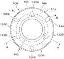
図1に示すように、本実施例のICトークン100は、中央部に配置されたコイン形ICタグモジュール102、コイン形ICタグモジュールの102の外周を囲うように配置された電磁波吸収リング104、及び、電磁波吸収リング104の全周を覆い、かつ、ICタグモジュール102を支える被覆樹脂部106からなる。As shown in FIG. 1, the
まずコイン形ICタグモジュール102を図2〜4を参照して説明する。
コイン形ICタグモジュール102は、内部にICタグ108をインサート成型した樹脂製の円盤である。
この樹脂は、例えば、剛性が高く、熱的電気的性質に優れたポリフェニレンスルフィド(PPS)である。First, the coin-shaped
The coin-shaped
This resin is, for example, polyphenylene sulfide (PPS) having high rigidity and excellent thermal and electrical properties.
ICタグ108は、ICチップと無線通信用のアンテナを組み合わせた超小型であって、少なくとも読取装置を使って、ICチップに記憶されたデータを読み取ることができる。
本実施例のICタグ108は、図4に示すように、フィルム状のシート110にICチップ112、及び、ICチップ112に接続した円形リング状のアンテナ114を貼付して一体化してある。
シート110を用いずに、アンテナ114にICチップ112を一体化したICタグ等も使用することができる。
As shown in FIG. 4, the
Without using the
図3に示すように、ICタグモジュール102は、ICタグ108を被覆するポリフェニレンスルフィド樹脂の被覆部116を有し、外形が円盤形であって、中央部が最も厚く、周縁に向かって徐々に薄くなっている。
換言すれば、ICタグモジュール102は碁石形である。
ICタグ108は、ICタグモジュール102の厚み方向及び径方向の中央に配置されている。As shown in FIG. 3, the
In other words, the
The
次に、電磁波吸収リング104を説明する。
電磁波吸収リング104は、電磁波を吸収し、かつ、ICトークン100に所定の強度を付与する機能を有する。
電磁波吸収リング104は、ICタグ108に外部から作用する電磁波、及び、ICタグから周方向へ発信する電磁波を吸収し、減衰させる機能を有し、ICタグモジュール102の周縁のほぼ全周の外側に配置される。
電磁波吸収リング104は、円形のリング部118、及びリング部118から所定の間隔で内方に半円形に突出する保持部120A、120B、120Cが形成されている。
本実施例では、最も数を少なくし、かつ、ICタグモジュール102の保持をするため、3つの保持部120A、120B、120Cが等間隔で配置されている。
なお、リング部118は、四角形等の多角形であってもよい。Next, the electromagnetic
The electromagnetic
The electromagnetic
The electromagnetic
In the present embodiment, in order to minimize the number and hold the
The
これら保持部120A、120B、120Cで囲まれた領域にICタグモジュール102が配置されている。
詳細には、ICタグモジュール102が保持部120A、120B、120C間に圧入され、所定の摩擦力で三点保持されている。
換言すれば、保持部は、円形の孔であっても良いが、被覆樹脂部106の成形時にリング部118からICタグ108への熱伝導が可及的に少なくなるように、接触面積が極力小さくなるようにすることが好ましい。The
Specifically,
In other words, the holding portion may be a circular hole, but the contact area is as small as possible so that the heat conduction from the
換言すれば、保持部120A、120B、120Cは、内向きに突出していることが好ましい。
保持部が実施例の三箇所である場合、ICタグモジュール102の保持力が安定し、最も好ましいが、2箇所であってもよい。
また、保持部は4箇所以上であってもよいが、射出成型時に電磁波吸収リング104からICタグモジュール102への伝導熱を可及的に少なくするため、より少ないことが好ましい。In other words, the holding
When there are three holding portions in the embodiment, the holding force of the
Further, although the number of holding portions may be four or more, it is preferable that the number of holding portions is smaller in order to minimize the heat of conduction from the electromagnetic
この保持部120A、120B、120Cには、成型型にセットする際の位置決め孔122A、122B、122Cが形成されている。
実施例における位置決め孔122A、122B、122Cは、円形であるが、四角形等角形であってもよい。
保持部120A、120B、120Cに位置決め孔122A、122B、122Cを形成することにより、リング部118と保持部120A、120B、120Cとの接続面積が小さくなり、リング部118からICタグモジュール102への伝導熱がさらに少なくなる利点がある。
しかし、位置決め孔122A、122B、122Cは、リング部118に配置することができる。The holding
The positioning holes 122A, 122B, and 122C in the embodiment are circular, but may be quadrilateral isometric.
By forming the positioning holes 122A, 122B, 122C in the holding
However, the positioning holes 122A, 122B, 122C can be disposed in the
さらに、リング部118には、三つの通孔124A、124B、124Cが等間隔で位置決め孔122A、122B、122Cに対し所定の間隔で形成されている。
通孔124A、124B、124Cは、射出成型時に後述の注入口からの樹脂がリング部118の背面側に流入しやすくするための機能を有する。
したがって、通孔124A、124B、124Cが無くとも樹脂が電磁波吸収リング104の全周に良好に回り込む場合、設ける必要はない。
また、前記目的が達成出来る場合、通孔の数及び位置は適当に設定することができる。
また、図5に示すように、電磁波吸収リング104のリング部118にすり割り126を形成することができる。
スリ割り126を形成した場合、電磁波吸収リング104の電磁波吸収効果が減少する。
したがって、ICトークン100との通信可能域を大きくする場合、スリ割り126を有する電磁波吸収リング104を用いることができる。Further, three through
The through
Therefore, even if the through
Moreover, when the said objective can be achieved, the number and position of a through-hole can be set appropriately.
Further, as shown in FIG. 5, a
When the
Therefore, when increasing the communicable area with the
電磁波吸収リング104は、電磁波吸収材料にて形成される。
電磁波吸収材料は、所定の強度及び重量を得るため、比重が大きい金属を用いることが好ましい。
また、電磁波吸収率を高めるため、金属の中でも強磁性体を用いることが好ましい。
さらに、安価であり、加工性に優れた鉄を用いることが好ましい。
鉄の他、真鍮、銅、白銅及びステンレスは、入手性がよく、比重が大きく、かつ、比較的安価であり、使用に適している。
電磁波吸収リング104が金属で作られる場合、打ち抜きプレスにより1行程又は2行程にて作ることができ、安価につくることができる。
なお、電磁波吸収リング104が金属の場合、発錆を防止するためメッキを施すことができる。
しかし、電磁波吸収材料であれば、金属以外の材料、例えば、カーボン繊維構造体を使用することができる。The electromagnetic
The electromagnetic wave absorbing material is preferably a metal having a large specific gravity in order to obtain a predetermined strength and weight.
In order to increase the electromagnetic wave absorption rate, it is preferable to use a ferromagnetic material among the metals.
Furthermore, it is preferable to use iron that is inexpensive and excellent in workability.
In addition to iron, brass, copper, white copper, and stainless steel are highly available, have a large specific gravity, and are relatively inexpensive, and are suitable for use.
When the electromagnetic
When the electromagnetic
However, if the electromagnetic wave absorbing material, material other than metal, for example, there can be used carbon fiber structure.
次に、被覆樹脂部106を説明する。
被覆樹脂部106は、電磁波吸収リング104の全周を覆い、かつ、ICタグモジュール102を支える機能を有する。
具体的には、図2及び3に示すように、電磁波吸収リング104の両側面及び外周面を所定の厚さで覆い、かつ、ICタグモジュール102の周縁端部の両側面を覆っている。
換言すれば、ICタグモジュール102の中央部は、被覆樹脂部106によって覆われていない。Next, the
The
Specifically, as shown in FIGS. 2 and 3, both side surfaces and the outer peripheral surface of the electromagnetic
In other words, the central portion of the
また、厳密には保持部120A、120B、120CとICタグモジュール102の外周との圧接部は被覆樹脂部106によって覆われないので、被覆樹脂部106は電磁波吸収リング104の全周を完全に覆っていない。
また、後述の保持ピン142又は位置決め保持ピン155が成型時に成型空間から抜かれない場合、それらと接する電磁波吸収リング104の一部は被覆樹脂106によって覆われない。
しかし、本発明において、電磁波吸収リング104の全周を覆う被覆樹脂部106の意味において、これらの僅かに覆わないこれらのケースを含むものである。
被覆樹脂部106は、ICタグモジュール102の被覆部116と同一の樹脂を用いることが好ましい。
なぜなら、被覆樹脂部106を成型する際、射出された高熱樹脂によってICタグモジュール102の被覆部116の表層が融解され、被覆樹脂部106と融合してICタグモジュール102を強力に保持しうるからである。Strictly speaking, the press contact portion between the holding
In addition, when a later-described
However, in the present invention, in the meaning of the covering
The covering
This is because when the covering
したがって、被覆樹脂部106は、その外周面124が円柱状であるので、後述のICトークン選別装置の傾斜ガイドレール168上を転がり易い。
また、電磁波吸収リング104の側面に対応する側面128及び130は、平坦に形成される。
したがって、成型型に文字、絵等を突部又は凹部により形成することにより、又は、成型後、スタンプ等により着色すること、更には、別に作成したシールを貼付することにより、側面128、130に装飾を施すことが容易にできる。Accordingly, since the outer
Further, the side surfaces 128 and 130 corresponding to the side surfaces of the electromagnetic
Therefore, by forming letters, pictures, etc. on the molding die with protrusions or recesses, or coloring with a stamp after molding, and further sticking a separately created seal to the side surfaces 128, 130 It can be easily decorated.
ICタグモジュール102の側面は、被覆樹脂部106の側面128及び130よりも僅かに奥部に位置している。
したがって、ICタグモジュール102が直接他の部位と接触する機会は極めて少ない。
よって、ICタグモジュール102が脱落する恐れがほとんど無い利点がある。
なお、この奥部に位置するICタグモジュール102の側面にプリントシールを貼付することにより、ICトークン100の装飾性を高めることができる。The side surface of the
Therefore, there is very little opportunity for the
Therefore, there is an advantage that the
Note that by sticking a printed seal on the side surface of the
次に被覆樹脂部106の射出成形型装置が図6を参照して説明される。
被覆樹脂部106は、ICタグモジュール102が電磁波吸収リング104に嵌め込まれ、一体化された状態で下型132にセットされる。
下型132には、ICタグモジュール102の中央部側面に密着するよう同一形状に形成した、皿状の下側モジュール保持部134が形成されている。
下側モジュール保持部134の下方の下型132内に下側冷却室136が形成されている。
下側冷却室136には、冷却装置(図示せず)を介して冷却液が供給され、強制的に下型132を冷却する。
したがって、下側冷却室136は、下型132を人為的に冷却する強制冷却装置138である。Next, an injection mold apparatus for the
The
The
A
The
Therefore, the
なお、本明細書において冷却とは、型内に射出された樹脂を冷却する意味である。
したがって、「樹脂を冷却」の意味において、下型132及び後述の上型146を加熱する場合も含むものである。
具体的には、射出する樹脂の流動性及びICタグモジュール102に悪影響を与えないよう射出成型時にICタグモジュール102を冷却することを満足する範囲の温度に保つことを意味する。In this specification, cooling means cooling the resin injected into the mold.
Therefore, in the meaning of “cool the resin”, the case where the
Specifically, this means that the temperature of the
電磁波吸収リング104は、下型132の成型凹部140に配置される。
このとき、成型凹部140の位置決め孔122A、122B、122Cに対応する底部の所定の位置から位置決め孔122A、122B、122Cにそれぞれ挿入することができる、位置決めピン142が突出している。
この位置決めピン142は、溶解樹脂が成型空間に射出される前に自動的に下型132内に引っ込み、その先端が成型凹部140の底面と面一になって被覆樹脂部106に孔が出来ないようにする。The electromagnetic
At this time, positioning pins 142 that can be inserted into the positioning holes 122A, 122B, and 122C respectively from predetermined positions on the bottom corresponding to the positioning holes 122A, 122B, and 122C of the
The
したがって、ICタグモジュール102と電磁波吸収リング104とを一体化した基材モジュール144を型にセットする場合、位置決め孔122A、122B、122Cを位置決めピン142に合わせてICタグモジュール102の下面が下側モジュール保持部134に密着するまで押し込む。
これにより、電磁波吸収リング104は、その内周面、下面及び外周面が下型132の凹部140と所定の間隔を持って保持される。Therefore, when the
Thus, the electromagnetic
しかし、位置決めピン142が固定され、射出成型された場合、その孔が側面130に残るようにすることができる。
その場合、位置決め孔122A、122B、122Cの内面が目視可能であるので、装飾性を高めるため、位置決め孔122A、122B、122Cにメッキを施すことができる。However, when the
In that case, since the inner surfaces of the positioning holes 122A, 122B, and 122C are visible, the positioning holes 122A, 122B, and 122C can be plated in order to improve the decorativeness.
次いで、上型146を下型132に対しセットする。
これにより、ICタグモジュール102の上面は同一形状に形成された上側モジュール保持部148と密接する。
上側モジュール保持部148の直ぐ近くの上型146にも、上側冷却室150が形成され、冷却液が下側冷却室136同様に供給される。
なお、下側冷却室136又は上側冷却室150のどちらか一方のみの設置でICタグモジュール102を十分に冷却出来る場合、どちらか一方のみを設ければよい。Next, the
Thereby, the upper surface of the
The
Note that if only one of the
この状態で、通孔124A、124B、124Cのそれぞれに上型の一部の注入口152の端面が相対する。
射出された樹脂が、通孔124A、124B、124Cを通って下型132と電磁波吸収リング104の下面との間に進入しやすくするためであるが、必要に応じ設けないことが出来る。
上型146がセットされた状態において、上型146の突状の成型面と電磁波吸収リング104の上面及び内周面との間に所定の成型空間が形成される。In this state, the end surfaces of the injection holes 152 that are part of the upper mold face the respective through
This is to make it easier for the injected resin to enter between the
In a state where the
次いで、複数の注入口152から成型空間に溶融樹脂を注入することにより、電磁波吸収リング104の周囲に樹脂が充填される。
結果として、電磁波吸収リング104の全周が樹脂で被覆される。
また、ICタグモジュール102は下側冷却室136及び上側冷却室150の冷却液によって強制的に冷却される。
換言すれば、ICタグ108のICチップ112が冷却され、耐熱温度以上になることを防止される。
したがって、被覆樹脂部106を成型する際、ICタグ108が機能的に破壊されることがない。Next, the resin is filled around the electromagnetic
As a result, the entire circumference of the electromagnetic
Further, the
In other words, the
Therefore, when the
成型後、上型146が下型132から離され、成型されたICトークン100が押し出しピン(図示せず)により押し出され、離型される。
なお、被覆樹脂部106の成型時に、電磁波吸収リング104の位置を所定の位置に保持できない場合、上型146及び下型132の相対位置から支えピン154U及び154Bをそれぞれ突出させ、それらの端面により挟んで保持することにより、電磁波吸収リング104の振動を防止することができ、所定の位置に保持することができる。After molding, the
If the position of the electromagnetic
また、図6(B)に図示するように、段部155を形成した支えピン154Cを固定状態に配置することが出来る。
この場合、電磁波吸収リング104の位置決め孔122A、122B、122Cを支えピン154Cの小径部に嵌め合わせ、段部155によって電磁波吸収リング104を支えるようにしてもよい。
この場合、被覆樹脂部106には、支えピン154Cによる穴のみであるので外観上に優れると共に、型装置が安価である利点がある。Further, as illustrated in FIG. 6 (B), it can be arranged support pins 154C forming the
In this case, the positioning holes 122A, 122B, 122C of the electromagnetic
In this case, since the
次に図7を参照してICトークン100の製造手順を説明する。
まず、最初に図7(A)に示すように、ICタグモジュール102を準備する。
このICタグモジュール102は、基材メーカーから購入、又は、自己にて製造する。
次に、図7(B)に示すように、ICタグモジュール102を保持部120A、120B、120Cの先端間に圧入し、電磁波吸収リング104とICタグモジュール102とを一体化し、基材モジュール144を製造する。Next, the manufacturing procedure of the
First, as shown in FIG. 7A, an
The
Next, as shown in FIG. 7B, the
次に、この基材モジュール144を恒温室に放置し、電磁波吸収リング104を所定の温度に加熱することが好ましい。
換言すれば、射出された樹脂が電磁波吸収リング104に沿って成型空間を流動し易いよう射出樹脂との温度差が所定の範囲になるよう調節する。
しかし、この行程は成型空間における樹脂の流動を確保できる場合、省略することができる。Next, it is preferable that the
In other words, the temperature difference from the injected resin is adjusted to a predetermined range so that the injected resin can easily flow in the molding space along the electromagnetic
However, this step can be omitted if the resin flow in the molding space can be secured.
次に、図7(D)に示すように、下型132に対し、基材モジュール144を位置決め孔122A、122B、122Cに位置決めピン142が嵌り合うよう位置決めし、ICタグモジュール108の下面が下側モジュール保持部134に密に接触するまで押し込む。Next, as shown in FIG. 7D, the
次に図7(E)に示すように上型146をセットする。
これにより、電磁波吸収リング104の周囲に樹脂成形空間が形成され、かつ、注入口152と相対して通孔124A、124B、124Cが自動的に位置される。
支えピン154B、154Uが使用される場合、それら支えピンが上下から自動的に進行し、それら先端間で電磁波吸収リング104を保持する。
樹脂の射出前に位置決めピン142は下型132内に戻される。Next, the
As a result, a resin molding space is formed around the electromagnetic
When the support pins 154B and 154U are used, the support pins automatically advance from above and below, and hold the electromagnetic
The positioning pins 142 are returned into the
次に、複数の注入口152から樹脂が射出され、被覆樹脂部106が成型される。
その後、上型146が上方に移動され、ICトークン100が離型される。
支えピン154B、154Uが使用された場合、上型146を下型から離す前に支えピン154U、154Bを下型132及び上型146内に引っ込める。Next, resin is injected from the plurality of
Thereafter, the
When the support pins 154B and 154U are used, the support pins 154U and 154B are retracted into the
次に、本発明に係るICトークン100を処理するために好ましい選別装置160が図8を参照して説明される。
選別装置160は、例えばゲーム機162に内蔵される。
選別装置160の前面に縦長スリット形の投入口164が形成される。Next, a
The
A vertical slit-shaped
この投入口164の長手寸法は、ICトークン100の直径よりも僅かに大きく、幅はICトークン100の厚みよりも僅かに大きく形成されている。
したがって、ICトークン100の直径又は幅よりも大きいサイズのトークンは投入口164に投入することができない。The longitudinal dimension of the
Therefore, a token having a size larger than the diameter or width of the IC token 100 cannot be inserted into the
投入口164に続いて投入口164から遠ざかる方向に伸びる傾斜通路166が形成される。
この傾斜通路166は、下流側ほど下になる下向き傾斜ガイドレール168によって形成されている。
また、下向きガイドレール168の両側には、ICトークン100の幅よりも僅かに間隔を開けてガイド側壁(図示せず)が配置される。
これらガイド側壁の一方は、ジャムしたICトークン100を返却口173に戻すため、傾斜通路166の幅を広げるよう移動可能である。Following the
The
Further, on both sides of the
One of these guide side walls is movable to increase the width of the
したがって、ICトークン100は傾斜通路166において、その側面をガイド側壁に案内されつつ、傾斜ガイドレール168上を転動する。
この傾斜通路166において、材質センサ170がガイド側壁に固定されている。
材質センサ170は、電磁波吸収リング104の材質を検知する機能を有する。
材質センサ170は、例えばコイルであり、電磁波吸収リング104が通過する側方に配置される。Therefore, IC token 100 in the
In the
The
The
傾斜通路166における材質センサ170の下流の側壁に、ICトークン100のICタグ108と通信するためのアンテナ172が取り付けられる。
アンテナ172は、図8(B)に示すように、板状の基板174にプリントされており、その長さ、換言すれば傾斜ガイドレール168に沿った長さは、ICタグ108のアンテナ114の直径の2倍以上に形成されている。
理由は、転動するICトークン100との通信時間を長くするためである。Downstream of the side wall of the
As shown in FIG. 8B, the
The reason is to increase the communication time with the rolling
したがって、アンテナ172は、投入口164から遠い位置、換言すれば、ゲーム機162の外部から遠い位置に配置される。
本発明のICトークン100は、ICタグ108の周囲が電磁波吸収リング104によって囲われているので、周方向の電磁波は吸収される。
傾斜ガイドレール168上を転動するICトークン100は、外周面124がゲーム機162の外部に向いている。
したがって、選別装置160に投入されたICトークン100に対し、ゲーム機162の外部から不正アクセスし、記憶情報を改ざんすることができない。Therefore, the
The
Therefore, unauthorized access to the IC token 100 inserted into the
傾斜通路166の下流には、上下方向に伸びる振分通路176が設けられ、振分ゲート178が配置される。
振分ゲート178は、通常スプリング(図示せず)によって振分通路176に突出される。
したがって、傾斜通路166から落下した偽貨や異なるゲーム場のICトークンは、振分ゲート178によって返却通路180に案内され、返却口173に戻される。A
The sorting
Accordingly, the false coins that have dropped from the
受け入られるべきICトークン100は、ゲート178がソレノイド182によって振分通路176から退出させられるため、受入口184に落下し、保留部(図示せず)に保留される。
受入口184にICトークン100が落下する途上において、ICトークン100は受入センサ186によって検知される。
受入センサ186は、例えば、ICコイン100によって接触子188が押動されるマイクロスイッチ190である。The
The
The
次に選別装置160の判別ユニット194を説明する。
判別ユニット194は、マイクロプロセッサ196であり、ROM198に記憶されたプログラムに基づいてRAM200に随時情報を書き込み、読み込みしつつ所定の処理を行う。Next, the
The
詳述すれば、材質センサ170からの信号、アンテナ172から読込ユニット202を介してICタグ108のICチップ112に記憶されている情報を読み込んで受け入れすべきICトークン100であるかどうかを判別する。
受け入れすべきトークン100である場合、前述のようにソレノイド182をドライバ204を介して所定時間励磁し、ゲート178を振分通路176から退出させて受入口184へ落下させる。More specifically, the signal from the
When the token 100 is to be received, the
また、材質センサ170及び読込ユニット202から信号を受けて受け入れるべきICトークン100であると判別した後、所定時間の間に受入センサ186から信号を受けた場合、入金信号をゲーム機162に出力し、ゲームのスタートが可能な状態にする。In addition, after receiving a signal from the
なお、マイクロプロセッサ196の出力に基づいて書込ユニット206及びアンテナ172を介してICタグ108に記憶されている情報を書き換えることができる。
例えば、ICトークン100に1000円に相当する価値情報が記憶されている場合、
一回投入される毎に100円に相当する価値情報を減算し、書き込むことが出来る。Incidentally, it is possible to rewrite the information stored in the
For example, if value information equivalent to 1000 yen is stored in the
Every time it is inserted, value information equivalent to 100 yen can be subtracted and written.
この場合、ICトークン100に記憶されている価値情報がゼロになった場合、ドライバ204を介してソレノイド182を励磁し、ゲート178を振分通路176から退出させて受入口184に落下させ、その他の場合、ソレノイド182を励磁させることなく、返却通路180を介して返却口173に戻すことができる。
なお、材質センサ170は、受け入れるべきICトークンの選別精度を高める場合等、必要に応じて使用することができる。
換言すれば、材質センサ170は、選択的に配置される。In this case, when the value information stored in the
The
In other words, the
100 ICトークン
102 コイン形ICタグモジュール
104 電磁波吸収リング
106 被覆樹脂部
108 ICタグ
112 ICチップ
114 アンテナ
120A、120B、120C 保持部
132、146 型
134、148 保持部
142 位置決めピン
154 保持ピン
164 投入口
168 傾斜ガイドレール
170 材質センサ
172 アンテナ
173 返却口
178 振り分けゲート
184 受入口
194 判別ユニット
202 読込ユニット100 IC token
102 Coin IC tag module
104 Electromagnetic wave absorbing ring
106 Coating resin part
108 IC tag
112 IC chip
114 Antenna
120A, 120B, 120C Holding part
132, 146 type
134, 148 Holding part
142 Locating pin
154 Holding pin
164 slot
168 Inclined guide rail
170 Material sensor
172 antenna
173 Return port
178 Sorting gate
184 Entrance
194 discrimination unit
202 Reading unit
Claims (3)
Translated fromJapanese前記電磁波吸収リングは内向きに等間隔で突出する3つの保持部(120A、120B、120C)を有し、前記コイン形ICタグモジュールの周縁が前記保持部の先端間に圧入されて保持され、
前記電磁波吸収リングの全周が前記被覆樹脂部により被覆され、さらに前記被覆樹脂部は前記コイン形ICタグモジュールの両側面を覆っていることを特徴とするICトークン。Ametal electromagnetic wave absorbing ring (104) is arranged on the outer periphery of a coin-shaped IC tag module (102) including an IC chip (112) and an antenna (114), and the coin-shaped IC tag module and the electromagnetic wave absorbing ring are connected to the electromagnetic wave. In theIC token integrated with the coating resin part (106) that covers the entire circumference of the absorption ring,
The electromagnetic wave absorbing ring has three holding portions (120A, 120B, 120C) protruding inward at equal intervals, and the periphery of the coin-shaped IC tag module is press-fitted between the tips of the holding portions and is held,
An IC token,wherein the entire circumference of the electromagnetic wave absorbing ring is covered with the coating resin portion, and the coating resin portion covers both side surfaces of the coin-shaped IC tag module .
前記電磁波吸収リングは内向きに等間隔で突出する3つの保持部(120A、120B、120C)を有し、前記コイン形ICタグモジュールの周縁が前記保持部の先端間に圧入されて保持され、
前記電磁波吸収リングの全周が前記被覆樹脂部により被覆され、さらに前記被覆樹脂部は前記コイン形ICタグモジュールの両側面を覆っているICトークンの射出成型型装置において、
前記コイン形ICタグモジュールの両面の夫々を保持する一対のモジュール保持部(134、148)を有し、かつ、前記電磁波吸収リング(104)の周囲に前記被覆樹脂部(106)を形成するための一対の型(132、146)の少なくとも一方を強制冷却型にし、
前記コイン形ICタグモジュールが嵌め込まれ一体化された前記電磁波吸収リングに形成された位置決め孔(122A,122B,122C)に嵌り合い前記一方のモジュール保持部に対し所定位置に位置決めする位置決めピン(142)を有するICトークンの射出成型型装置。Ametal electromagnetic wave absorbing ring (104) is arranged on the outer periphery of a coin-shaped IC tag module (102) including an IC chip (112) and an antenna (114), and the coin-shaped IC tag module and the electromagnetic wave absorbing ring are connected to the electromagnetic wave. In theIC token integrated with the coating resin part (106) that covers the entire circumference of the absorption ring,
The electromagnetic wave absorbing ring has three holding portions (120A, 120B, 120C) protruding inward at equal intervals, and the periphery of the coin-shaped IC tag module is press-fitted between the tips of the holding portions and is held,
The entire circumference of the electromagnetic wave absorbing ring is covered with the coating resin portion, and the coating resin portion further covers the both sides of the coin-shaped IC tag module in an IC token injection mold device,
A pair of module holding portion (134,148) for holding each of both surfaces of the coin-shaped IC tag module, and, for formingthe coating resin portion around said electromagnetic wave absorbing ring (104) (106) At least one of the pair of molds (132, 146) is a forced cooling mold,
Positioning pins (142) that fit into positioning holes (122A, 122B, 122C) formed in the electromagnetic wave absorption ring in which the coin-shaped IC tag module is fitted and integrated and are positioned at a predetermined position with respect to theone module holding portion. IC token injection mold device.
前記リング(104)と一体化した前記コイン形ICタグモジュールの面を一対の型(132、146)にて保持するとともに前記リングの周囲に樹脂装填空間を前記型にて形成し、
かつ、前記リングを前記一対の型からそれぞれ突出する支えピン(154U、154B)の端面により挟んで保持した後、前記装填空間に樹脂を装填することを特徴とするICトークンの製造方法。The outer periphery of the coin-shaped IC tag module (102) is an inward projection of ametal ring (104)made of an electromagnetic wave absorbing material, andthree holding portions (120A, 120B, 120C) and is heldby press fitbetween integral,
Holding the surface of the coin-shaped IC tag module integrated with thering (104) with apair of molds (132, 146) and forming a resin loading space around the ring with the mold,
The method of manufacturing an IC token is characterized in that the ringis heldbetween the end faces of the support pins (154U, 154B) protruding from the pair of molds, and then the resin is loaded into the loading space.
Priority Applications (3)
| Application Number | Priority Date | Filing Date | Title |
|---|---|---|---|
| JP2004381357AJP4709989B2 (en) | 2004-12-28 | 2004-12-28 | IC token, IC token injection mold apparatus, and IC token manufacturing method |
| GB0523258AGB2421877B (en) | 2004-12-28 | 2005-11-15 | IC token, injecting molding die device for IC token, method for manufacturing IC token, selection device for IC token |
| US11/318,670US20060160628A1 (en) | 2004-12-28 | 2005-12-27 | IC token, injection molding die for the IC token manufacturing method for the IC token and an IC token selection device |
Applications Claiming Priority (1)
| Application Number | Priority Date | Filing Date | Title |
|---|---|---|---|
| JP2004381357AJP4709989B2 (en) | 2004-12-28 | 2004-12-28 | IC token, IC token injection mold apparatus, and IC token manufacturing method |
Publications (2)
| Publication Number | Publication Date |
|---|---|
| JP2006185397A JP2006185397A (en) | 2006-07-13 |
| JP4709989B2true JP4709989B2 (en) | 2011-06-29 |
Family
ID=35516964
Family Applications (1)
| Application Number | Title | Priority Date | Filing Date |
|---|---|---|---|
| JP2004381357AExpired - Fee RelatedJP4709989B2 (en) | 2004-12-28 | 2004-12-28 | IC token, IC token injection mold apparatus, and IC token manufacturing method |
Country Status (3)
| Country | Link |
|---|---|
| US (1) | US20060160628A1 (en) |
| JP (1) | JP4709989B2 (en) |
| GB (1) | GB2421877B (en) |
Families Citing this family (15)
| Publication number | Priority date | Publication date | Assignee | Title |
|---|---|---|---|---|
| US20080113774A1 (en)* | 2006-11-10 | 2008-05-15 | Christine Denlay | Sentinel/guard for protecting a predefined gaming area |
| JP2008246103A (en)* | 2007-03-30 | 2008-10-16 | Angel Shoji Kk | Game token including rfid and its manufacturing method |
| JP5331378B2 (en)* | 2007-05-29 | 2013-10-30 | 株式会社半導体エネルギー研究所 | Card game machine |
| JP5425447B2 (en)* | 2008-11-19 | 2014-02-26 | 株式会社ユニバーサルエンターテインメント | GAME CHIP AND GAME SYSTEM |
| JP5335471B2 (en)* | 2009-02-18 | 2013-11-06 | 株式会社中京遊技 | Game medal with identification information |
| US8665094B2 (en) | 2009-07-23 | 2014-03-04 | System Integration Technology Korea Co., Ltd. | RFID tag-embedded casino chip |
| KR100959902B1 (en)* | 2009-07-23 | 2010-05-26 | 주식회사 에스아이티코리아 | Casino chip with rfid tag |
| DE102011105847A1 (en)* | 2011-05-17 | 2012-11-22 | Saxonia Eurocoin Gmbh | Biteilige coin with a core of plastic |
| US10226688B1 (en)* | 2014-08-27 | 2019-03-12 | Frank A. Camaratta, Jr. | Chess pieces weighted with powdered metal |
| US9514594B1 (en)* | 2015-08-11 | 2016-12-06 | Comdata, Inc. | Metallic stored value token and method of manufacture |
| TWI609329B (en) | 2016-12-19 | 2017-12-21 | 韋僑科技股份有限公司 | Rfid device and method for making the same |
| JP7003592B2 (en)* | 2017-11-16 | 2022-02-04 | 凸版印刷株式会社 | Coin type IC tag |
| RU2706655C1 (en)* | 2019-01-28 | 2019-11-19 | Акционерное общество "Гознак" (АО "Гознак") | Polymer-containing composite protected article |
| DE102019130175A1 (en)* | 2019-11-08 | 2021-05-12 | Hellermanntyton Gmbh | Injection molding of a component, such as a cable holder, with an integrated wireless identification film |
| PH12022552805A1 (en)* | 2020-04-20 | 2024-03-25 | Angel Group Co Ltd | Gaming chip and method for manufacturing the same |
Family Cites Families (14)
| Publication number | Priority date | Publication date | Assignee | Title |
|---|---|---|---|---|
| GB1399422A (en)* | 1972-01-17 | 1975-07-02 | Int Cybernetic Machines Ltd | Coin testing device |
| US5166502A (en)* | 1990-01-05 | 1992-11-24 | Trend Plastics, Inc. | Gaming chip with implanted programmable identifier means and process for fabricating same |
| ES2095021T5 (en)* | 1993-10-18 | 2006-05-01 | Gemplus | ELECTRONIC PURCHASING GAMES MACHINE. |
| US6121544A (en)* | 1998-01-15 | 2000-09-19 | Petsinger; Julie Ann | Electromagnetic shield to prevent surreptitious access to contactless smartcards |
| US6296190B1 (en)* | 1999-05-03 | 2001-10-02 | Trend Plastics, Inc. | Gaming chip with transponder and a method for making same |
| BR9907298A (en)* | 1999-05-15 | 2000-10-24 | Kde Inc | RF card and device for your reading |
| JP2000331132A (en)* | 1999-05-25 | 2000-11-30 | Hitachi Maxell Ltd | IC token and reader / writer |
| JP3534042B2 (en)* | 2000-06-21 | 2004-06-07 | オムロン株式会社 | Coin-shaped IC tag and method of manufacturing the same |
| JP2002024775A (en)* | 2000-07-06 | 2002-01-25 | Nippon Conlux Co Ltd | Coin type ic card reader/writer |
| AUPQ873400A0 (en)* | 2000-07-13 | 2000-08-03 | Dolphin Advanced Technologies Pty Limited | Improved gaming chip |
| JP2002150364A (en)* | 2000-11-09 | 2002-05-24 | Nippon Conlux Co Ltd | Coin handling device |
| JP2003331250A (en)* | 2002-03-05 | 2003-11-21 | Mitsubishi Materials Corp | Small disk with rfid |
| JP4028763B2 (en)* | 2002-06-17 | 2007-12-26 | 日立マクセル株式会社 | Non-contact communication type information carrier |
| JP2004141490A (en)* | 2002-10-25 | 2004-05-20 | Aruze Corp | Game media lending machines and gaming machines |
- 2004
- 2004-12-28JPJP2004381357Apatent/JP4709989B2/ennot_activeExpired - Fee Related
- 2005
- 2005-11-15GBGB0523258Apatent/GB2421877B/ennot_activeExpired - Fee Related
- 2005-12-27USUS11/318,670patent/US20060160628A1/ennot_activeAbandoned
Also Published As
| Publication number | Publication date |
|---|---|
| GB2421877B (en) | 2010-03-03 |
| JP2006185397A (en) | 2006-07-13 |
| GB2421877A (en) | 2006-07-05 |
| US20060160628A1 (en) | 2006-07-20 |
| GB0523258D0 (en) | 2005-12-21 |
Similar Documents
| Publication | Publication Date | Title |
|---|---|---|
| JP4709989B2 (en) | IC token, IC token injection mold apparatus, and IC token manufacturing method | |
| US5676376A (en) | Composite gaming chip | |
| EP0232174B1 (en) | Tokens and apparatus for handling tokens | |
| JP2003331250A (en) | Small disk with rfid | |
| CN105358005B (en) | Valuable token with the embedding core comprising radio frequency identification and electromagnetic detection feature | |
| EP2016447A1 (en) | Identification tags, objects adapted to be identified, and related methods, devices and systems | |
| JP2007310696A (en) | Ic token | |
| US20040173434A1 (en) | Coin-like products, identification method thereof and identification device thereof | |
| RU2213374C2 (en) | Bimetal coin discriminator | |
| US5908103A (en) | Token with Wiegand wire | |
| JP2004227133A (en) | Detector of coin receiving device | |
| JP4403231B2 (en) | Coin sorting device with smart card billing function | |
| WO1996018173A2 (en) | Coin or similar legal tender with an electromagnetic component and method for manufacturing same | |
| JP4130991B2 (en) | Coin with identification information | |
| KR20030096685A (en) | Card for exchanging for a Gift and Method for Preventing from Counterfeiting the Card | |
| JP2004089462A (en) | Illicitness preventive system of game token for pachinko slot machine | |
| CN1516080A (en) | detecting device of coin receiver | |
| JP4134339B2 (en) | Bimetal coin selector | |
| JP2009207694A (en) | Counter | |
| JP7134600B2 (en) | Coin type IC tag | |
| TWM351413U (en) | Coin refund structure for learning type coin machine | |
| ITRM20110176U1 (en) | COIN DETECTION DEVICE. | |
| JP3140749U (en) | Game media counter using IC tag | |
| KR20100023981A (en) | Credit card having contents and drviving method thereof | |
| JP4747276B2 (en) | Game machine medal and medal game machine using the medal |
Legal Events
| Date | Code | Title | Description |
|---|---|---|---|
| A621 | Written request for application examination | Free format text:JAPANESE INTERMEDIATE CODE: A621 Effective date:20071129 | |
| A977 | Report on retrieval | Free format text:JAPANESE INTERMEDIATE CODE: A971007 Effective date:20101001 | |
| A131 | Notification of reasons for refusal | Free format text:JAPANESE INTERMEDIATE CODE: A131 Effective date:20101013 | |
| A521 | Request for written amendment filed | Free format text:JAPANESE INTERMEDIATE CODE: A523 Effective date:20101209 | |
| TRDD | Decision of grant or rejection written | ||
| A01 | Written decision to grant a patent or to grant a registration (utility model) | Free format text:JAPANESE INTERMEDIATE CODE: A01 Effective date:20110223 | |
| A61 | First payment of annual fees (during grant procedure) | Free format text:JAPANESE INTERMEDIATE CODE: A61 Effective date:20110223 | |
| R150 | Certificate of patent or registration of utility model | Ref document number:4709989 Country of ref document:JP Free format text:JAPANESE INTERMEDIATE CODE: R150 | |
| R250 | Receipt of annual fees | Free format text:JAPANESE INTERMEDIATE CODE: R250 | |
| R250 | Receipt of annual fees | Free format text:JAPANESE INTERMEDIATE CODE: R250 | |
| R250 | Receipt of annual fees | Free format text:JAPANESE INTERMEDIATE CODE: R250 | |
| R250 | Receipt of annual fees | Free format text:JAPANESE INTERMEDIATE CODE: R250 | |
| R250 | Receipt of annual fees | Free format text:JAPANESE INTERMEDIATE CODE: R250 | |
| R250 | Receipt of annual fees | Free format text:JAPANESE INTERMEDIATE CODE: R250 | |
| R250 | Receipt of annual fees | Free format text:JAPANESE INTERMEDIATE CODE: R250 | |
| R250 | Receipt of annual fees | Free format text:JAPANESE INTERMEDIATE CODE: R250 | |
| R250 | Receipt of annual fees | Free format text:JAPANESE INTERMEDIATE CODE: R250 | |
| R250 | Receipt of annual fees | Free format text:JAPANESE INTERMEDIATE CODE: R250 | |
| LAPS | Cancellation because of no payment of annual fees |