JP4708577B2 - Method for manufacturing thin film semiconductor device - Google Patents
Method for manufacturing thin film semiconductor deviceDownload PDFInfo
- Publication number
- JP4708577B2 JP4708577B2JP2001023848AJP2001023848AJP4708577B2JP 4708577 B2JP4708577 B2JP 4708577B2JP 2001023848 AJP2001023848 AJP 2001023848AJP 2001023848 AJP2001023848 AJP 2001023848AJP 4708577 B2JP4708577 B2JP 4708577B2
- Authority
- JP
- Japan
- Prior art keywords
- layer
- semiconductor
- thin film
- semiconductor device
- manufacturing
- Prior art date
- Legal status (The legal status is an assumption and is not a legal conclusion. Google has not performed a legal analysis and makes no representation as to the accuracy of the status listed.)
- Expired - Fee Related
Links
Images


Classifications
- H—ELECTRICITY
- H01—ELECTRIC ELEMENTS
- H01L—SEMICONDUCTOR DEVICES NOT COVERED BY CLASS H10
- H01L21/00—Processes or apparatus adapted for the manufacture or treatment of semiconductor or solid state devices or of parts thereof
- H01L21/02—Manufacture or treatment of semiconductor devices or of parts thereof
- H01L21/04—Manufacture or treatment of semiconductor devices or of parts thereof the devices having potential barriers, e.g. a PN junction, depletion layer or carrier concentration layer
- H01L21/18—Manufacture or treatment of semiconductor devices or of parts thereof the devices having potential barriers, e.g. a PN junction, depletion layer or carrier concentration layer the devices having semiconductor bodies comprising elements of Group IV of the Periodic Table or AIIIBV compounds with or without impurities, e.g. doping materials
- H01L21/30—Treatment of semiconductor bodies using processes or apparatus not provided for in groups H01L21/20 - H01L21/26
- H01L21/302—Treatment of semiconductor bodies using processes or apparatus not provided for in groups H01L21/20 - H01L21/26 to change their surface-physical characteristics or shape, e.g. etching, polishing, cutting
- H01L21/304—Mechanical treatment, e.g. grinding, polishing, cutting
- H—ELECTRICITY
- H01—ELECTRIC ELEMENTS
- H01L—SEMICONDUCTOR DEVICES NOT COVERED BY CLASS H10
- H01L21/00—Processes or apparatus adapted for the manufacture or treatment of semiconductor or solid state devices or of parts thereof
- H01L21/02—Manufacture or treatment of semiconductor devices or of parts thereof
- H01L21/02104—Forming layers
- H01L21/02107—Forming insulating materials on a substrate
- H01L21/02109—Forming insulating materials on a substrate characterised by the type of layer, e.g. type of material, porous/non-porous, pre-cursors, mixtures or laminates
- H01L21/02203—Forming insulating materials on a substrate characterised by the type of layer, e.g. type of material, porous/non-porous, pre-cursors, mixtures or laminates the layer being porous
- H—ELECTRICITY
- H01—ELECTRIC ELEMENTS
- H01L—SEMICONDUCTOR DEVICES NOT COVERED BY CLASS H10
- H01L21/00—Processes or apparatus adapted for the manufacture or treatment of semiconductor or solid state devices or of parts thereof
- H01L21/02—Manufacture or treatment of semiconductor devices or of parts thereof
- H01L21/02104—Forming layers
- H01L21/02107—Forming insulating materials on a substrate
- H01L21/02225—Forming insulating materials on a substrate characterised by the process for the formation of the insulating layer
- H01L21/02227—Forming insulating materials on a substrate characterised by the process for the formation of the insulating layer formation by a process other than a deposition process
- H01L21/0223—Forming insulating materials on a substrate characterised by the process for the formation of the insulating layer formation by a process other than a deposition process formation by oxidation, e.g. oxidation of the substrate
- H01L21/02233—Forming insulating materials on a substrate characterised by the process for the formation of the insulating layer formation by a process other than a deposition process formation by oxidation, e.g. oxidation of the substrate of the semiconductor substrate or a semiconductor layer
- H01L21/02236—Forming insulating materials on a substrate characterised by the process for the formation of the insulating layer formation by a process other than a deposition process formation by oxidation, e.g. oxidation of the substrate of the semiconductor substrate or a semiconductor layer group IV semiconductor
- H01L21/02238—Forming insulating materials on a substrate characterised by the process for the formation of the insulating layer formation by a process other than a deposition process formation by oxidation, e.g. oxidation of the substrate of the semiconductor substrate or a semiconductor layer group IV semiconductor silicon in uncombined form, i.e. pure silicon
- H—ELECTRICITY
- H01—ELECTRIC ELEMENTS
- H01L—SEMICONDUCTOR DEVICES NOT COVERED BY CLASS H10
- H01L21/00—Processes or apparatus adapted for the manufacture or treatment of semiconductor or solid state devices or of parts thereof
- H01L21/02—Manufacture or treatment of semiconductor devices or of parts thereof
- H01L21/02104—Forming layers
- H01L21/02107—Forming insulating materials on a substrate
- H01L21/02225—Forming insulating materials on a substrate characterised by the process for the formation of the insulating layer
- H01L21/02227—Forming insulating materials on a substrate characterised by the process for the formation of the insulating layer formation by a process other than a deposition process
- H01L21/02255—Forming insulating materials on a substrate characterised by the process for the formation of the insulating layer formation by a process other than a deposition process formation by thermal treatment
- H—ELECTRICITY
- H01—ELECTRIC ELEMENTS
- H01L—SEMICONDUCTOR DEVICES NOT COVERED BY CLASS H10
- H01L21/00—Processes or apparatus adapted for the manufacture or treatment of semiconductor or solid state devices or of parts thereof
- H01L21/02—Manufacture or treatment of semiconductor devices or of parts thereof
- H01L21/02104—Forming layers
- H01L21/02107—Forming insulating materials on a substrate
- H01L21/02296—Forming insulating materials on a substrate characterised by the treatment performed before or after the formation of the layer
- H01L21/02299—Forming insulating materials on a substrate characterised by the treatment performed before or after the formation of the layer pre-treatment
- H01L21/02307—Forming insulating materials on a substrate characterised by the treatment performed before or after the formation of the layer pre-treatment treatment by exposure to a liquid
- H—ELECTRICITY
- H01—ELECTRIC ELEMENTS
- H01L—SEMICONDUCTOR DEVICES NOT COVERED BY CLASS H10
- H01L21/00—Processes or apparatus adapted for the manufacture or treatment of semiconductor or solid state devices or of parts thereof
- H01L21/02—Manufacture or treatment of semiconductor devices or of parts thereof
- H01L21/02104—Forming layers
- H01L21/02107—Forming insulating materials on a substrate
- H01L21/02296—Forming insulating materials on a substrate characterised by the treatment performed before or after the formation of the layer
- H01L21/02318—Forming insulating materials on a substrate characterised by the treatment performed before or after the formation of the layer post-treatment
- H01L21/02337—Forming insulating materials on a substrate characterised by the treatment performed before or after the formation of the layer post-treatment treatment by exposure to a gas or vapour
- H—ELECTRICITY
- H01—ELECTRIC ELEMENTS
- H01L—SEMICONDUCTOR DEVICES NOT COVERED BY CLASS H10
- H01L21/00—Processes or apparatus adapted for the manufacture or treatment of semiconductor or solid state devices or of parts thereof
- H01L21/02—Manufacture or treatment of semiconductor devices or of parts thereof
- H01L21/04—Manufacture or treatment of semiconductor devices or of parts thereof the devices having potential barriers, e.g. a PN junction, depletion layer or carrier concentration layer
- H01L21/18—Manufacture or treatment of semiconductor devices or of parts thereof the devices having potential barriers, e.g. a PN junction, depletion layer or carrier concentration layer the devices having semiconductor bodies comprising elements of Group IV of the Periodic Table or AIIIBV compounds with or without impurities, e.g. doping materials
- H01L21/30—Treatment of semiconductor bodies using processes or apparatus not provided for in groups H01L21/20 - H01L21/26
- H01L21/302—Treatment of semiconductor bodies using processes or apparatus not provided for in groups H01L21/20 - H01L21/26 to change their surface-physical characteristics or shape, e.g. etching, polishing, cutting
- H01L21/306—Chemical or electrical treatment, e.g. electrolytic etching
- H01L21/3063—Electrolytic etching
- H—ELECTRICITY
- H01—ELECTRIC ELEMENTS
- H01L—SEMICONDUCTOR DEVICES NOT COVERED BY CLASS H10
- H01L21/00—Processes or apparatus adapted for the manufacture or treatment of semiconductor or solid state devices or of parts thereof
- H01L21/70—Manufacture or treatment of devices consisting of a plurality of solid state components formed in or on a common substrate or of parts thereof; Manufacture of integrated circuit devices or of parts thereof
- H01L21/77—Manufacture or treatment of devices consisting of a plurality of solid state components or integrated circuits formed in, or on, a common substrate
- H01L21/78—Manufacture or treatment of devices consisting of a plurality of solid state components or integrated circuits formed in, or on, a common substrate with subsequent division of the substrate into plural individual devices
- H—ELECTRICITY
- H01—ELECTRIC ELEMENTS
- H01L—SEMICONDUCTOR DEVICES NOT COVERED BY CLASS H10
- H01L2221/00—Processes or apparatus adapted for the manufacture or treatment of semiconductor or solid state devices or of parts thereof covered by H01L21/00
- H01L2221/67—Apparatus for handling semiconductor or electric solid state devices during manufacture or treatment thereof; Apparatus for handling wafers during manufacture or treatment of semiconductor or electric solid state devices or components; Apparatus not specifically provided for elsewhere
- H01L2221/683—Apparatus for handling semiconductor or electric solid state devices during manufacture or treatment thereof; Apparatus for handling wafers during manufacture or treatment of semiconductor or electric solid state devices or components; Apparatus not specifically provided for elsewhere for supporting or gripping
- H01L2221/68304—Apparatus for handling semiconductor or electric solid state devices during manufacture or treatment thereof; Apparatus for handling wafers during manufacture or treatment of semiconductor or electric solid state devices or components; Apparatus not specifically provided for elsewhere for supporting or gripping using temporarily an auxiliary support
- H01L2221/68363—Apparatus for handling semiconductor or electric solid state devices during manufacture or treatment thereof; Apparatus for handling wafers during manufacture or treatment of semiconductor or electric solid state devices or components; Apparatus not specifically provided for elsewhere for supporting or gripping using temporarily an auxiliary support used in a transfer process involving transfer directly from an origin substrate to a target substrate without use of an intermediate handle substrate
- H—ELECTRICITY
- H01—ELECTRIC ELEMENTS
- H01L—SEMICONDUCTOR DEVICES NOT COVERED BY CLASS H10
- H01L2224/00—Indexing scheme for arrangements for connecting or disconnecting semiconductor or solid-state bodies and methods related thereto as covered by H01L24/00
- H01L2224/01—Means for bonding being attached to, or being formed on, the surface to be connected, e.g. chip-to-package, die-attach, "first-level" interconnects; Manufacturing methods related thereto
- H01L2224/42—Wire connectors; Manufacturing methods related thereto
- H01L2224/47—Structure, shape, material or disposition of the wire connectors after the connecting process
- H01L2224/48—Structure, shape, material or disposition of the wire connectors after the connecting process of an individual wire connector
- H01L2224/4805—Shape
- H01L2224/4809—Loop shape
- H01L2224/48091—Arched
- H—ELECTRICITY
- H01—ELECTRIC ELEMENTS
- H01L—SEMICONDUCTOR DEVICES NOT COVERED BY CLASS H10
- H01L2924/00—Indexing scheme for arrangements or methods for connecting or disconnecting semiconductor or solid-state bodies as covered by H01L24/00
- H01L2924/01—Chemical elements
- H01L2924/01067—Holmium [Ho]
- H—ELECTRICITY
- H01—ELECTRIC ELEMENTS
- H01L—SEMICONDUCTOR DEVICES NOT COVERED BY CLASS H10
- H01L2924/00—Indexing scheme for arrangements or methods for connecting or disconnecting semiconductor or solid-state bodies as covered by H01L24/00
- H01L2924/10—Details of semiconductor or other solid state devices to be connected
- H01L2924/102—Material of the semiconductor or solid state bodies
- H01L2924/1025—Semiconducting materials
- H01L2924/10251—Elemental semiconductors, i.e. Group IV
- H01L2924/10253—Silicon [Si]
- H—ELECTRICITY
- H01—ELECTRIC ELEMENTS
- H01L—SEMICONDUCTOR DEVICES NOT COVERED BY CLASS H10
- H01L2924/00—Indexing scheme for arrangements or methods for connecting or disconnecting semiconductor or solid-state bodies as covered by H01L24/00
- H01L2924/10—Details of semiconductor or other solid state devices to be connected
- H01L2924/11—Device type
- H01L2924/13—Discrete devices, e.g. 3 terminal devices
- H01L2924/1304—Transistor
- H01L2924/1305—Bipolar Junction Transistor [BJT]
Landscapes
- Engineering & Computer Science (AREA)
- Physics & Mathematics (AREA)
- Condensed Matter Physics & Semiconductors (AREA)
- General Physics & Mathematics (AREA)
- Manufacturing & Machinery (AREA)
- Computer Hardware Design (AREA)
- Microelectronics & Electronic Packaging (AREA)
- Power Engineering (AREA)
- Dicing (AREA)
- Thin Film Transistor (AREA)
Description
Translated fromJapanese【0001】
【発明の属する技術分野】
本発明は薄膜半導体装置、及びその製造方法の関わる。
【0002】
【従来の技術】
LSIチップを薄層化するため、シリコン基板に集積回路等を形成した後、基板裏面側からグラインダーにより薄層化する技術が知られている。
【0003】
しかし、集積回路等が形成される層はシリコン基板の表面のみであり、大部分の領域が研削され捨てられてしまう。これでは限りある資源の有効活用とはいえない。一方では、半導体装置の微細化・高集積化に伴いチップ発熱密度が飛躍的に大きくなることが懸念され、早急にLSIチップを薄層化する技術の確立が求められている。
【0004】
また、通常の半導体チップ自体にはフレキシブル性が無く、ICカードなど薄型デバイスに搭載する際には、曲げ強度を高める必要がある。これは、ICカードのように携帯される場合には、収容時に曲げの力が加わる場合があるからである。
従って、薄型デバイスに搭載されるLSIチップ等にもその放熱性及び機械的柔軟性の点から薄層化が求められる。
【0005】
特開平9−312349号公報には、LSIチップのフレキシブル化の為ために多孔質層による分離を利用した技術が記載されている。
【0006】
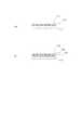
具体的には図4(a)示すように半導体基体11上に多孔質層12を介してデバイス形成層10を設け、該デバイス形成層と保持基板16とを接着剤17を介して貼り合せる。その後、半導体基体11と保持基板16との間に両者を引き離す方向の外力を与える。すると、機械的強度の弱い多孔質層12で分離が生じ、半導体基体11から保持基板16とともにデバイス形成層12が剥離する(図4(b))。
【0007】
次に剛性を有する保持基板16側に面方向の引っ張りによって延伸するダイシング用フィルム18を接合する。そして、ダイシング装置によってデバイス形成層側から切り込み溝19を形成するダイシング作業を行う(図4(c))。その後、ダイシング用フィルムを面方向にのばして各チップに分断する。こうして、薄層化されたLSIチップが出来上がる。
【0008】
【発明が解決しようとする課題】
しかしながら、上記LSIチップの薄層化技術では、保持基板との接着工程やダイシング用フィルムとの接合工程などの複数の工程を経なければならない。
【0009】
更に、分離する際にデバイス形成層全体が繋がっていると、その一部に局所的に歪み等が加わりデバイス特性に影響を及ぼす場合がある。
【0010】
本発明の目的は上記問題点に鑑み、少ない工程で、且つ分離の際のデバイス形成層への影響を少なくした薄膜半導体装置、及びその製造方法を提供することにある。更に、一度薄膜半導体装置の製造に使用した部材を、再度その製造に利用することができる経済的な薄膜半導体装置の製造方法を提供することをも目的とする。
【0011】
【課題を解決するための手段】
本発明に係る薄膜半導体装置の製造方法は、半導体領域上に分離層、前記分離層上に半導体素子及び/又は半導体集積回路を備えた半導体膜を有する部材を用意する工程と、前記部材の前記半導体膜側から切り込み溝を、前記切り込み溝の先端が、前記半導体領域、前記分離層内部あるいは前記半導体膜と前記分離層との界面に位置するように形成する溝形成工程と、前記溝形成工程後、前記分離層に熱、振動、又は外力を加えることにより、前記分離層において前記半導体素子及び/又は半導体集積回路の領域の一部を前記部材から分離する分離工程と、を有することを特徴とする。
【0012】
特に前記分離工程を、前記切り込み溝に流体を注入することにより行うことができる。
【0013】
ここで、前記部材は、半導体基板表面に多孔質層を形成し、且つ該多孔質層表面に前記半導体膜を形成した後、前記半導体素子及び/又は半導体集積回路を形成して得られる。あるいは半導体基板表面に前記半導体素子及び/又は半導体集積回路を形成した後、該表面側から所定深さにイオンを注入して前記分離層を形成して得られる。
【0014】
前記切り込み溝は、前記半導体膜に形成してもよいし、あるいは前記半導体素子及び/又は半導体集積回路を前記半導体膜に形成する過程において作製された領域に形成してもよい。
【0015】
また、前記切り込み溝の先端が、前記分離層内部、あるいは前記半導体膜と前記分離層との界面に位置するように該切り込み溝を形成することができる。更にまた、前記部材が、半導体領域上に前記分離層、及び前記半導体膜を有している場合に、前記切り込み溝の先端が、前記分離層と該半導体領域の界面、あるいは該半導体領域内部に位置するように該切り込み溝を形成してもよい。
【0016】
前記分離工程は、前記切り込み溝から高圧の流体を注入することにより行われたり、あるいは液体あるいは気体からなる前記流体を、前記切り込み溝の少なくとも一部に噴きつけることにより行われる。前記分離工程を静圧下で行うこともできる。前記分離工程により前記領域の一部が複数のチップにチップ化することもできる。
【0017】
なお、前記部材から前記領域の一部が分離された後に残る残留部材を用いて、前記部材を再度作製することもできる。
【0018】
本発明においては、半導体素子や半導体集積回路素子が形成されたデバイス層を部材から分離する前に、切り込み溝を形成し、そして流体を用いて領域の一部を分離するので、きわめて効率的にかつデバイス層に影響を与えることなく半導体装置の薄層化が可能となる。
【0019】
【発明の実施の形態】
本発明の主たる実施形態につき図1を用いて説明する。
【0020】
まず、図1(a)に示すように、半導体領域130上に分離層100を介して半導体膜110を有する部材120を用意する。そして、上記半導体膜110に半導体素子及び/又は半導体集積回路140を形成する(図1(b))。そして、半導体素子及び/又は半導体集積回路140をチップ化するに先だって、所望の位置に、上記半導体膜110側から切り込み溝150を形成する。
【0021】
その後、所望の半導体素子又は半導体集積回路140を上記分離層100を利用して分離する。分離工程は、例えば切り込み溝150の少なくとも一部に流体を注入することにより分離を行うことができる。あるいは、分離する所望領域を真空チャック等で保持した後、その領域に超音波振動を印加して分離層で分離したり、あるいは所望領域に局所的に熱を印加して分離することもできる。
【0022】
こうしてチップ化された、単数あるいは複数の薄膜半導体装置160が得られる(図1(d))。
【0023】
薄膜半導体装置160に分離層100の一部が残留する場合には、当該残留部分を研磨、研削あるいはエッチング等により除去した後、他の回路との接続、あるいはパッケージングを行うことができる。勿論、当該残留部分を残したまま、パッケージングを行ってもよい。即ち、図1(e)のように残留分離層101を介して支持基体170上に薄膜半導体装置160を載置したり、図1(f)のように、プラスチックカード上に移設することもできる。なお、180は封入用樹脂、190はワイヤ、200は封止樹脂/フィルム、210はプラスチックカードである。また、分離層がゲッタリングサイトになり、プロセス中の金属汚染耐性が増す。
【0024】
(分離層)なお、分離層100は、具体的には単結晶シリコンウエハ表面の陽極化成により形成される多孔質シリコン層や、単結晶シリコンウエハの所望の深さに水素、ヘリウム、希ガス等のイオンを注入して形成されるイオン注入層である。
【0025】
前者の場合には、部材120を形成するには、多孔質シリコン層上にCVD法等を用いて単結晶シリコンなどの非多孔質薄膜を成長させる。また、分離層100を多孔度の異なる複数の層で構成することもできる。例えば、図2(a)に示すように、半導体領域130側から高多孔度層310、低多孔度層300と2層の構成にしてもよいし、あるいは半導体領域130側から低多孔度層320、高多孔度層330、低多孔度層340と3層構成にすることもできる。高多孔度層の場合の多孔度は、10%から90%、低多孔度層の場合の多孔度は、0%から70%の範囲で利用可能である。多孔度の異なる複数の層の形成は、陽極化成の際の電流密度を変えたり、化成溶液の種類あるいは濃度を変えることで実現できる。
【0026】
陽極化成により多孔質層を形成した場合には、該多孔質層上へ半導体膜110を成長させるに先だって、多孔質の孔の内壁に窒化膜あるいは酸化膜などの保護膜を設ける保護膜形成工程、や水素を含む雰囲気中での熱処理工程を行うのがよい。勿論、上記保護膜形成工程後、前記熱処理工程を行うことも好ましい。
【0027】
更に、CVD法により半導体膜110を成長させる場合には、所定の厚み(例えば10nm)までは、20nm/min.以下の低成長速度で行うのがよい。
【0028】
(半導体膜)また、半導体膜110としては、非多孔質単結晶シリコン薄膜や、GaAs、InP、GaN等の化合物半導体膜を用いることができる。半導体膜が単結晶シリコンの場合に原料ガスとして、SiH2Cl2、SiHCl3、SiCl4、SiH4、あるいはHClガスを添加しても良い。形成方法はCVD法に限らず、MBE法、スパッター法等も可能である。
【0029】
なお、多孔質層を水素を含む雰囲気中で第1の熱処理した後、薄膜を成長させるに先だって当該第1の熱処理温度よりも高い温度で第2の熱処理することも好ましいものである。第1の熱処理温度としては、800℃〜1000℃、第2の熱処理温度として、900℃〜融点の範囲で利用できる。これにより多孔質層表面の孔の封止が十分行われるのである。例えば、第1の熱処理温度を950℃で行い、第2の熱処理を1100℃で行うことができる。
【0030】
(部材)また、部材120としては、CZ法、MCZ法、あるいはFZ法などで作製された単結晶シリコンウエハのみならず、基板表面が水素アニール処理されたウエハ、あるいはエピタキシャルシリコンウエハなどを用いることができる。勿論、シリコンに限らずGaAs基板やInP基板等の化合物半導体基板も用いることができる。
【0031】
(半導体素子及び/又は半導体集積回路)また、半導体素子及び/又は半導体集積回路140としては、CMOS、バイポーラトランジスタ、ダイオード、コイル、キャパシタ等の素子、DRAM、マイクロプロセッサー、ロジックIC、メモリ等の半導体集積回路を作製することができる。素子や回路の用途としては、電子回路、発振回路、受・発光素子、光導波路、各種センサーなどを含む。
【0032】
(切り込み溝)また、切り込み溝150は、通常用いられるダイシング装置を用いることができる他、エッチングやレーザーアブレーション、超音波カッター、高圧ジェット(例えば、ウォータージェット)、超音波カッターなども用いることができる。エッチングにより行う場合は、HF+H2O2、HF+HNO3、アルカリ溶液などのエッチング液を用いることができる。レーザーとしては、YAGレーザー、CO2レーザー、エキシマレーザー等である。
【0033】
切り込み溝の先端は、半導体領域130に達しても構わないが、好ましくは分離層100の内部、あるいは半導体膜110と分離層100との界面付近に達することが好ましい。分離層が高多孔度層と低多孔度層を含み形成される場合には、高多孔度層の内部あるいはその界面付近に切り込み溝の先端が達するのが好ましい。
【0034】
なお、切り込み溝を形成する先だって、分離後は個々のチップになる当該チップ間を、LOCOS(局所酸化)あるいはメサエッチングし、チップ間には半導体膜が存在しないようにしておいてもよい。
【0035】
(分離)また、分離方法としては、分離したい箇所、すなわち複数のチップ化された部分の所望のチップを取り囲む切り込み溝150の少なくとも一部に液体や気体等の流体を注入することにより行うことができる。ここでいう、流体を注入するとは、高圧の流体ジェットを噴きつける場合や、静圧下での分離をも含むものである。各チップの周囲の切り込み溝に流体を噴きつける場合は、所望のチップ毎に分離できるし、静圧下の場合は、複数のチップをまとめて、即ち複数個を一度に分離することも可能である。かかる場合には、分離に先だって各チップを支持する支持部材にあらかじめ貼り合わせておくことも好ましいものである。なお、流体に超音波を印加しておくことも可能である。流体としては、液体として水、エッチング液、アルコールなど、気体としては空気、窒素ガス、アルゴンガス等である。
【0036】
流体を切り込み溝に吹きつけて分離する場合の一例について、具体的に説明する。なお、ノズルを2つ用いて分離する場合について説明するが、流体の圧力等を制御して分離できさえすれば、以下の分離方法に限定されるものではない。
【0037】
図3(a)は、半導体領域430上に分離層としての多孔質層400を介して半導体膜410が形成され、更に当該半導体膜に半導体素子又は半導体集積回路440が形成されている場合を示している。ここで、441は、絶縁キャップ層である。図3(b)に示すように切り込み溝450を形成する。同図においては切り込み溝449、450の先端が多孔質層の内部に位置する場合を示している。チップ460を半導体領域430から剥離する場合、チップ保持手段452で保持しつつ、ノズル451及び454から流体453、455を切り込み溝に向けて噴射する。流体は切り込み溝の先端まで達した後、横方向に拡がろうとするので(456〜459は流体の流れを模式的に示すものである。)それぞれの切り込み溝449、450から進入した流体457、458が重なるとチップ460は半導体領域430から剥離する(図3(d))。多孔質層内で多孔度の変化がある場合には、より剥離しやすくする為に切り込み溝の先端部付近を境に多孔度が変わるように分離層を形成しておくのがよい。そして、チップ保持手段452で保持したまま半導体領域430上から移設する(図3(e))。次にチップ470を剥離したい場合は、ノズル454からは流体を噴きつけず、ノズル451のみから切り込み溝471に流体を吹きつけることのみにより剥離を行ってもよい(図3(f))。
【0038】
なお、チップ保持手段452として、真空チャック、切り込み溝で挟み込むようにして保持することができる。さらに、分離するチップを真空チャック等で保持した後、そのチップに超音波振動を印加して分離する。
流体を切り込み溝に噴きつける場合は、チップの周囲を取り囲む切り込み溝のうち、相対向する溝の2箇所に噴きつけてもよいし、チップのコーナー部分の1箇所に噴きつけることもできる。
【0039】
また、切り込み溝の形成により微小領域に区分けされた所望領域を真空チャック等で保持した後その領域に超音波振動を印加したり、あるいは局所的に熱を印加することで分離することができる。とりわけ分離層を水素、窒素、He、希ガス等のイオン注入により作製した場合には、400℃から600℃程度の熱処理を施すことで、イオン注入により形成される微小気泡層が凝集するので斯かる現象を利用して分離することもできる。CO2レーザー等により加熱することもできる。あるいは、切り込み溝により微小領域に区分けされているので、所望領域を真空チャック等で保持したまま、引っ張り力、圧縮力、剪断力を加えることで分離することもできる。このように、分離前に微小領域に区分けしておくことで、外力により分離する際にも不必要な応力集中を避けることができる。微小領域としては、10cm×10cm以下、好ましくは5cm×5cm以下、更に好ましくは2cm×2cm以下が望ましい。
【0040】
(実施例1)
比抵抗0.01Ω・cmのP型の単結晶Si基板を用意し、HF溶液中において基板表面の陽極化成を行った。陽極化成条件は以下の通りであった。
【0041】
電流密度 :7(mA・cm−2)
陽極化成溶液 :HF:H2O:C2H5OH=1:1:1
時間 :11(分)
多孔質Si層の厚み :12(μm)
多孔質Si層は、当該多孔質Si層上に高品質エピタキシャルSi層を形成させることができ、さらに分離層として用いることができるよう多孔度を調整した。具体的には、20%であった。なお、多孔質Si層の厚さは、上記厚さに限らず、数百μmから0.1μm程度まで使用できる。
【0042】
この単結晶Si基板を400℃の酸素雰囲気中で1時間酸化した。これにより多孔質Siの孔の内壁は熱酸化膜で覆われた。その後、この多孔質Si層の表面をフッ酸に浸漬し、孔の内壁の酸化膜を残して、多孔質Si層の表面の酸化膜のみ除去した。次に多孔質Si層上にCVD(Chemical Vapor Deposition)法により単結晶Si層を3μmエピタキシャル成長した。成長条件は以下の通りである。
【0043】
ソースガス :SiH2Cl2/H2
ガス流量 :0.5/180 l/min
ガス圧力 :80Torr
温度 :950℃
成長速度 :0.3μm/min
エピタキシャル成長に先立って、水素含有雰囲気中の熱処理を行った。これは、表面孔を封止するためである。この熱処理に加えて、微小なSi原子を原料ガスなどにより添加し、その表面孔封止用の原子を補っても良い。
【0044】
こうして得られる部材は、通常用いられているエピウエハと同一のウエハとして扱うことが出来る。異なるのは、エピ層の下に多孔質Si層が形成されていることのみである。このエピ層に、マイクロプロセッサー、ロジックIC、メモリ、等の回路を作製した。LSIの作製は、通常と全く同じ工程を通すことにより、従来と同一の性能を持つLSIを作製できた。なお、エピ層にデバイスを形成するに先立って、エピ層を水素雰囲気中で熱処理することも好ましいものである。
【0045】
多孔質Siの残留Si領域は空乏化しており、高抵抗化されている。これにより一種SOI的なデバイスの高速化、低消費電力化が実現される。
【0046】
なお、素子分離としてトレンチを用いることにより、チップ面積の縮小が達成されウエハ内の取れ数も増大する。また、トレンチあるいはLOCOSを多孔質Si層まで達するようにすることにより、多孔質Si層の高抵抗性と合わせて、素子間絶縁性を達成することが出来た。
【0047】
次に、複数のチップに分ける為に、デバイス形成層側からダイシングを行い、切り込み溝を形成した。溝の先端は多孔質Si層の内部に位置していた。
【0048】
そして、流体として水を切り込み溝から吹きつけた。流体ジェットはチップの周囲の切り込み溝の2箇所から吹きつけた。こうして、チップが部材から分離された。既に周囲のチップが剥離されている場合には、一つのノズルから噴射される流体のみで分離できた。
【0049】
なお、流体には、気体、液体、あるいは、それらに固体の粒体・粉体を含有したものがある。この実施例では、ウォータージェット(以下「WJ」と記述する)を記述するが、エアージェット、窒素ガスジェット、その他気体ジェット、水以外の液体ジェット、氷やプラスチック片、研磨材の混ざった流体ジェット、あるいはこれらの静圧をかけることも可能である。流体は非常に微小な隙間へも流入し内部の圧力を上げることが可能で、外圧を分散して印加できることが特徴である。また、一部に極端に圧力がかからないことから、もっとも分離しやすい個所を選択的に分離させるという特徴がある。
【0050】
分離の際には、チップ表面を支持部材等で支持するのが好ましい。デバイス層側に残留した多孔質Siは、除去してもしなくても良い。
【0051】
その後、それぞれのチップをパッケージした。分離面をパッケージ台に乗せて、表面側からワイアーボンディングしても良いし、表面を伏せてパッケージしてもよい。なお、プラスチックカードに直接パッケージすることで、ICカードを作製することもできる。
【0052】
パッケージ台をヒートシンクとして用いれば、従来のバックグラインダー方式に比較して格段の熱放散性を有する。バックグラインダーによる裏面の薄層化は、通常数百ミクロンである。本発明では、表面のエピ層の厚さと多孔質Siの残留部の厚さ合計、即ち10μm程度以下しか残留しないため、デバイスの熱発生源とヒートシンクの距離が狭まり、熱放散性が格段に向上する。OEIC(Optoelectronic Integrated Circuits)をのエピ層に作製して、光透過性基板あるいは光導波路にパッケージすることもできる。
【0053】
なお、分離して残った単結晶Si基板は、必要に応じて表面再研磨、エッチング等を行い、再度同じ工程に投入できた。あるいは、別目的の基板として利用することもできる。
【0054】
(実施例2)
実施例1においては、多孔質層は1層であったが、本実施例においては、多孔度の異なる2層構成の多孔質層とした。
【0055】
まず、シリコン基板表面の陽極化成を以下の条件で行った。
【0056】
電流密度 :8(mA・cm−2)
陽極化成溶液 :HF:H2O:C2H5OH=1:1:1
時間 :5(分)
多孔質Si層の厚み :6(μm)
その後、以下の条件で陽極化成を行った。
【0057】
電流密度 :33(mA・cm−2)
陽極化成溶液 :HF:H2O:C2H5OH=1:1:1
時間 :80(秒)
多孔質Siの厚み :3(μm)
こうして、単結晶シリコン基板側から多孔度45%の高多孔度層、更にその上に20%の低多孔度層が形成された。その後、実施例1と同じ条件によりエピタキシャルシリコン層を低多孔度層上に形成し、更に集積回路等を形成した。次に、チップ化のためにエピタキシャル層側からダイシングを行った。切り込み溝の先端が前記高多孔度層と低多高度層の界面付近に位置するように制御した。そして、当該溝に水を噴射してチップを剥離することができた。分離は、上述の2層の多孔質層の界面付近で生じた。その他の要件は、実施例1と同様とした。
【0058】
なお、2層の多孔質層の厚さは、6μm/3μmの構成でなくてもよく、陽極化成条件を変えることによって、厚さを可変させることができる。また陽極化成液は、HF:H2O:C2H5OH=1:1:1でなくても良い。また、エタノールの代わりにIPA(イソプロピルアルコール)等の他のアルコールを用いても良い。アルコールは界面活性剤として反応泡のウエハ表面付着を防止することを目的としているので、アルコールでなくて他の界面活性剤でもよいし、界面活性剤を添加せずに超音波で表面付着泡を除去してもよい。
【0059】
なお、切り込み溝を形成した後、上記集積回路等のデバイス層を形成してもよい。
【0060】
(実施例3)
抵抗率14Ω・cmのP型の単結晶Si基板を用意した。面方位は<100>であった。この単結晶Si基板表面に、マイクロプロセッサー、ロジックIC、メモリ等の回路形成層を作製した。
【0061】
その後、回路形成層側から、所定の深さ(本実施例では、表面側から3μmの深さ)に水素イオンを注入してイオン注入層を形成した。注入量は、数E16からE17/cm2であった。注入に際して、最表面にSiO2などの保護膜を形成しておいてもよい。
【0062】
次に、ダイシングを行い所望領域に区分けされるよう切り込み溝を作製した。溝の先端はイオン注入層の内部に位置していた。その後、該切り込み溝からウォータージェットを噴きつけたところ複数のチップに分離することができた。
【0063】
また、切り込み溝にウォータージェットを噴きつけることなく、分離してチップ化したい領域に局所的にレーザー加熱を行うことでも分離できる。また、イオン注入層を形成する前に、切り込み溝を形成しておくことも可能である。
【0064】
なお、分離層をイオン注入により形成している場合は、400℃から600℃程度の加熱でイオン注入による微小空隙(マイクロキャビティ−)が凝集し分離が生じるので、通常800℃程度以上のプロセス温度が必要な集積回路等の形成は困難であるが、本実施例のようにイオン注入層の形成に先だって、デバイス層を形成しておくことで上記問題点が解消できる。
【0065】
(実施例4)
比抵抗0.01Ω・cmのP型の単結晶Si基板を用意し、HF溶液中において基板表面の陽極化成を行った。陽極化成条件は以下の通りであった。
【0066】
電流密度 :8(mA・cm−2)
陽極化成溶液 :HF:H2O:C2H5OH=1:1:1
時間 :5(分)
多孔質Si層の厚み :6(μm)
その後、以下の条件で陽極化成を行った。
【0067】
電流密度 :33(mA・cm−2)
陽極化成溶液 :HF:H2O:C2H5OH=1:1:1
時間 :80(秒)
多孔質Siの厚み :3(μm)
こうして、単結晶シリコン基板側から多孔度45%の高多孔度層、更にその上に20%の低多孔度層が形成された。その後、実施例1と同じ条件によりエピタキシャルシリコン層を低多孔度層上に形成し、更に集積回路等を形成した。次に、チップ化のためにエピタキシャル層側からダイシングを行い、微小領域に区分けした。切り込み溝の先端が前記高多孔度層と低多高度層の界面付近に位置するように制御した。
【0068】
次に、チップ化を図りたい領域の一部を真空ピンセット等の保持手段で保持しつつ、外力(本実施例においては、引っ張り力)により分離した。
【0069】
なお、分離の際に、圧縮力を加えた後、引っ張り力により剥がすなど、種々の外力を組み合わせたり、外力と流体とを組み合わせて分離を行うこともできる。
【0070】
【発明の効果】
本発明によれば、少ない工程で、且つ分離の際のデバイス形成層への影響を少なくした薄膜半導体装置を製造することができる。
【図面の簡単な説明】
【図1】本発明の実施形態の一例を示す模式的断面図である。
【図2】本発明における分離層の構成の一例を示す為の模式的断面図である。
【図3】本発明における分離工程の一例を示す模式的断面図である。
【図4】従来例を説明する為の模式的断面図である。
【符号の説明】
100 分離層
101 残留分離層
110 半導体膜
120 部材
130 半導体領域
140 半導体素子又は半導体集積回路
150 切り込み溝
160 薄膜半導体装置[0001]
BACKGROUND OF THE INVENTION
The present invention relates to a thin film semiconductor device and a manufacturing method thereof.
[0002]
[Prior art]
In order to reduce the thickness of an LSI chip, a technique is known in which an integrated circuit or the like is formed on a silicon substrate, and then the thickness is reduced by a grinder from the back side of the substrate.
[0003]
However, the layer on which the integrated circuit or the like is formed is only the surface of the silicon substrate, and most of the region is ground and discarded. This is not an effective use of limited resources. On the other hand, there is a concern that the heat generation density of the chip will increase dramatically with the miniaturization and high integration of the semiconductor device, and there is a need to establish a technology for making the LSI chip thinner as soon as possible.
[0004]
In addition, ordinary semiconductor chips themselves are not flexible, and when mounted on thin devices such as IC cards, it is necessary to increase the bending strength. This is because in the case of being carried like an IC card, a bending force may be applied during storage.
Accordingly, LSI chips and the like mounted on thin devices are also required to be thin from the viewpoint of heat dissipation and mechanical flexibility.
[0005]
Japanese Patent Application Laid-Open No. 9-312349 describes a technique using separation by a porous layer for making an LSI chip flexible.
[0006]
Specifically, as shown in FIG. 4A, the
[0007]
Next, a dicing film 18 that is stretched by pulling in the surface direction is bonded to the
[0008]
[Problems to be solved by the invention]
However, in the LSI chip thinning technology, a plurality of processes such as an adhesion process with a holding substrate and a bonding process with a dicing film must be performed.
[0009]
Furthermore, if the entire device formation layer is connected at the time of separation, distortion may be locally added to a part of the device formation layer, which may affect device characteristics.
[0010]
In view of the above-described problems, an object of the present invention is to provide a thin film semiconductor device that has a small number of steps and has less influence on a device formation layer at the time of separation, and a method for manufacturing the same. It is another object of the present invention to provide an economical method for manufacturing a thin film semiconductor device in which a member once used for manufacturing a thin film semiconductor device can be used again for the manufacture thereof.
[0011]
[Means for Solving the Problems]
Method of manufacturing a thin film semiconductor device according to the present invention,the separation layer on a semiconductor region, a step of preparing a member forhave a semiconductor element and / or a semiconductor film having a semiconductor integrated circuiton the separation layer,the member a groove cut fromthe semiconductor filmside, the tip of the cut groove, the semiconductor region, a groove forming step of formingso as to be located at the interface between the separation layer inside or the semiconductor film and the separation layer,the groove formed after step,heat to the separation layer, vibration, or by applying an external force, by having a separation step of separating a part of region ofthe semiconductor device and / or a semiconductor integrated circuit fromsaid memberat said separation layer Features.
[0012]
In particular, the separation step can be performed by injecting a fluid into the cut groove.
[0013]
Wherein said member is a porous layer formed on a semiconductor substrate surface, and after forming the semiconductor film on the porous layer surface,Ru obtained by forming the semiconductor elements and / or semiconductor integratedcircuit. Alternatively, after the semiconductor element and / or the semiconductor integrated circuit is formed on the surface of the semiconductor substrate, ions are implanted from the surface side to a predetermined depth to form the separation layer.
[0014]
The cut groove may be formed in the semiconductor film, or may be formed in a region formed in the process of forming the semiconductor element and / or the semiconductor integrated circuit in the semiconductor film.
[0015]
The tip of the cut groove, it is possible to form the notches to be positionedat the fieldsurface with the separation layer inside, or the semiconductor film and the separation layer. Furthermore, when the member has the separation layer and the semiconductor film on a semiconductor region, the tip of the cut groove is located at the interface between the separation layer and the semiconductor region, or inside the semiconductor region. The cut groove may be formed so as to be positioned.
[0016]
The separation step is performed by injecting a high-pressure fluid from the cut groove, or by spraying the fluid made of liquid or gas onto at least a part of the cut groove. The separation step can also be performed under static pressure.A part of the region may be formed into a plurality of chips by the separation step.
[0017]
In addition, the said member can also be produced again using the remaining member which remains aftera part of saidarea |region was isolate | separated from the said member.
[0018]
In the present invention, a notch groove is formed before a device layer on which a semiconductor element or a semiconductor integrated circuit element is formed is separated from a member, anda part of theregion is separated using a fluid. In addition, the semiconductor device can be thinned without affecting the device layer.
[0019]
DETAILED DESCRIPTION OF THE INVENTION
A main embodiment of the present invention will be described with reference to FIG.
[0020]
First, as shown in FIG. 1A, a
[0021]
Thereafter, a desired semiconductor element or semiconductor integrated
[0022]
In this way, one or a plurality of thin
[0023]
When a part of the
[0024]
(Separation layer) The
[0025]
In the former case, in order to form the
[0026]
When a porous layer is formed by anodization, a protective film forming step of providing a protective film such as a nitride film or an oxide film on the inner wall of the porous hole before growing the
[0027]
Further, when the
[0028]
(Semiconductor Film) As the
[0029]
Note that it is also preferable that after the first heat treatment of the porous layer in an atmosphere containing hydrogen, the second heat treatment is performed at a temperature higher than the first heat treatment temperature before the thin film is grown. The first heat treatment temperature may be 800 ° C. to 1000 ° C., and the second heat treatment temperature may be 900 ° C. to the melting point. As a result, the pores on the surface of the porous layer are sufficiently sealed. For example, the first heat treatment temperature can be performed at 950 ° C., and the second heat treatment can be performed at 1100 ° C.
[0030]
(Member) Further, as the
[0031]
(Semiconductor element and / or semiconductor integrated circuit) Also, as the semiconductor element and / or semiconductor integrated
[0032]
(Cut Groove) In addition, the
[0033]
The tip of the cut groove may reach the
[0034]
Prior to forming the cut groove, LOCOS (local oxidation) or mesa etching may be performed between the chips that become individual chips after separation so that no semiconductor film exists between the chips.
[0035]
(Separation) Further, as a separation method, itis performed by injecting a fluid such as a liquid or a gas into at least a part of a
[0036]
An example of the case where the fluid is blown into the cut groove and separated will be specifically described. In addition, although the case where it isolate | separates using two nozzles is demonstrated, as long as it can isolate | separate by controlling the pressure of a fluid etc., it is not limited to the following separation methods.
[0037]
FIG. 3 (a) shows a case where a semiconductor film 410 is formed on a semiconductor region 430 via a porous layer 400 as a separation layer, and a semiconductor element or a semiconductor integrated circuit 440 is further formed on the semiconductor film. ing. Here, 441 is an insulating cap layer. A cut groove 450 is formed as shown in FIG. 3 (b). In the same figure, the case where the front-end | tip of the notch grooves 449 and 450 is located inside a porous layer is shown. When the chip 460 is peeled from the semiconductor region 430, the fluids 453 and 455 are ejected from the nozzles 451 and 454 toward the cut groove while being held by the chip holding means 452. Since the fluid reaches the tip of the cut groove and then spreads in the lateral direction (456 to 459 schematically show the flow of the fluid), the fluid 457 entered from the respective cut grooves 449 and 450, When 458 overlaps, the chip 460 is separated from the semiconductor region 430 (FIG. 3D). When there is a change in porosity in the porous layer, it is preferable to form a separation layer so that the porosity changes with the vicinity of the tip of the cut groove as a boundary in order to make it easier to peel. Then, it is moved from above the semiconductor region 430 while being held by the chip holding means 452 (FIG. 3 (e)). Next, when the chip 470 is desired to be peeled off, the fluid may not be sprayed from the nozzle 454, but may be peeled only by spraying the fluid into the cut groove 471 only from the nozzle 451 (FIG. 3 (f)).
[0038]
The chip holding means 452 can be held by being sandwiched between a vacuum chuck and a cut groove. Furthermore, after the chip to be separated is held by a vacuum chuck or the like, the chip isseparated by applying ultrasonic vibration.
In the case of spraying the fluid into the cut groove, it may be sprayed to two locations of the opposed grooves among the cut grooves surrounding the periphery of the chip, or may be sprayed to one corner portion of the chip.
[0039]
Further, after a desired area divided into minute areas by holding a cut groove is held by a vacuum chuck or the like, it can be separated by applying ultrasonic vibration to the area or applying heat locally. In particular, when the separation layer is produced by ion implantation of hydrogen, nitrogen, He, a rare gas, or the like, the microbubble layer formed by ion implantation is aggregated by performing a heat treatment at about 400 ° C. to 600 ° C. Separation can also be performed using this phenomenon. It can also be heated by a CO2 laser or the like. Alternatively, since it is divided into minute regions by the cut grooves, it can be separated by applying a tensile force, a compressive force, and a shearing force while holding the desired region with a vacuum chuck or the like. As described above, by dividing into small regions before separation, unnecessary stress concentration can be avoided even when separation is performed by an external force. The minute region is 10 cm × 10 cm or less, preferably 5 cm × 5 cm or less, more preferably 2 cm × 2 cm or less.
[0040]
Example 1
A P-type single crystal Si substrate having a specific resistance of 0.01 Ω · cm was prepared, and the substrate surface was anodized in an HF solution. The anodizing conditions were as follows.
[0041]
Current density: 7 (mA · cm−2)
Anodizing solution: HF: H2O: C2H5OH = 1: 1: 1
Time: 11 (minutes)
Thickness of porous Si layer: 12 (μm)
The porosity of the porous Si layer was adjusted so that a high-quality epitaxial Si layer could be formed on the porous Si layer and used as a separation layer. Specifically, it was 20%. In addition, the thickness of the porous Si layer is not limited to the above-mentioned thickness, and it can be used from several hundred μm to about 0.1 μm.
[0042]
This single crystal Si substrate was oxidized in an oxygen atmosphere at 400 ° C. for 1 hour. As a result, the inner walls of the porous Si holes were covered with the thermal oxide film. Thereafter, the surface of the porous Si layer was immersed in hydrofluoric acid, and only the oxide film on the surface of the porous Si layer was removed leaving the oxide film on the inner wall of the hole. Next, a single crystal Si layer was epitaxially grown by 3 μm on the porous Si layer by CVD (Chemical Vapor Deposition). The growth conditions are as follows.
[0043]
Source gas: SiH2Cl2 / H2
Gas flow rate: 0.5 / 180 l / min
Gas pressure: 80 Torr
Temperature: 950 ° C
Growth rate: 0.3 μm / min
Prior to the epitaxial growth, a heat treatment in a hydrogen-containing atmosphere was performed. This is to seal the surface holes. In addition to this heat treatment, fine Si atoms may be added by a source gas or the like to supplement the atoms for sealing the surface holes.
[0044]
The member thus obtained can be handled as the same wafer as a commonly used epi-wafer. The only difference is that a porous Si layer is formed under the epi layer. Circuits such as a microprocessor, logic IC, and memory were fabricated on this epi layer. An LSI with the same performance as before could be manufactured by going through the same process as usual. It is also preferable to heat the epi layer in a hydrogen atmosphere prior to forming the device on the epi layer.
[0045]
The residual Si region of porous Si is depleted and has a high resistance. As a result, high speed and low power consumption of a kind of SOI device is realized.
[0046]
By using trenches for element isolation, the chip area can be reduced and the number of wafers in the wafer can be increased. In addition, by extending the trench or LOCOS to the porous Si layer, it was possible to achieve inter-element insulation in combination with the high resistance of the porous Si layer.
[0047]
Next, in order to divide into a plurality of chips, dicing was performed from the device forming layer side to form cut grooves. The tip of the groove was located inside the porous Si layer.
[0048]
Then, water was cut as a fluid and sprayed from the groove. The fluid jet was blown from two places in the notch groove around the chip. Thus, the chip was separated from the member. When the surrounding chip was already peeled off, it could be separated only by the fluid ejected from one nozzle.
[0049]
The fluid includes gas, liquid, or those containing solid particles / powder. In this embodiment, a water jet (hereinafter referred to as “WJ”) is described. However, an air jet, a nitrogen gas jet, other gas jets, a liquid jet other than water, ice, a plastic piece, a fluid jet mixed with abrasives. Alternatively, these static pressures can be applied. A feature of the fluid is that it can flow into a very small gap to increase the internal pressure, and the external pressure can be distributed and applied. In addition, there is a feature that a part that is most easily separated is selectively separated because a part of the pressure is not extremely applied.
[0050]
In the separation, the chip surface is preferably supported by a support member or the like. The porous Si remaining on the device layer side may or may not be removed.
[0051]
Then, each chip was packaged. The separation surface may be placed on a package base and wire-bonded from the surface side or may be packaged with the surface down. An IC card can also be manufactured by packaging directly on a plastic card.
[0052]
If the package base is used as a heat sink, the heat dissipation is much higher than that of the conventional back grinder system. The backside thinning with a back grinder is usually a few hundred microns. In the present invention, since the total thickness of the epi layer on the surface and the remaining thickness of the porous Si, that is, about 10 μm or less remains, the distance between the heat generation source of the device and the heat sink is narrowed, and the heat dissipation is remarkably improved. To do. OEIC (Optoelectronic Integrated Circuits) can be fabricated on an epi layer and packaged on a light transmissive substrate or an optical waveguide.
[0053]
The single crystal Si substrate remaining after separation was subjected to surface repolishing, etching and the like as needed, and could be put into the same process again. Alternatively, it can be used as a substrate for another purpose.
[0054]
(Example 2)
In Example 1, there was one porous layer, but in this example, a porous layer having a two-layer structure with different porosities was used.
[0055]
First, anodization of the silicon substrate surface was performed under the following conditions.
[0056]
Current density: 8 (mA · cm−2)
Anodizing solution: HF: H2O: C2H5OH = 1: 1: 1
Time: 5 (minutes)
Thickness of porous Si layer: 6 (μm)
Thereafter, anodization was performed under the following conditions.
[0057]
Current density: 33 (mA · cm−2)
Anodizing solution: HF: H2O: C2H5OH = 1: 1: 1
Time: 80 (seconds)
Porous Si thickness: 3 (μm)
Thus, a high porosity layer having a porosity of 45% was formed from the single crystal silicon substrate side, and a 20% low porosity layer was further formed thereon. Thereafter, an epitaxial silicon layer was formed on the low porosity layer under the same conditions as in Example 1, and an integrated circuit and the like were further formed. Next, dicing was performed from the epitaxial layer side for chip formation. The tip of the cut groove was controlled to be located in the vicinity of the interface between the high porosity layer and the low multi-altitude layer. And the chip | tip was able to be peeled by injecting water into the said groove | channel. Separation occurred near the interface between the two porous layers described above. Other requirements were the same as in Example 1.
[0058]
Note that the thickness of the two porous layers may not be 6 μm / 3 μm, and the thickness can be varied by changing the anodizing conditions. The anodizing solution may not be HF: H2O: C2H5OH = 1: 1: 1. Further, other alcohols such as IPA (isopropyl alcohol) may be used instead of ethanol. Alcohol is used as a surfactant to prevent the reaction foam from adhering to the wafer surface, so other surfactants may be used instead of alcohol, and the surface-adhered foam may be ultrasonically added without adding a surfactant. It may be removed.
[0059]
Note that a device layer such as the integrated circuit may be formed after the cut groove is formed.
[0060]
(Example 3)
A P-type single crystal Si substrate having a resistivity of 14 Ω · cm was prepared. The plane orientation was <100>. Circuit formation layers such as a microprocessor, a logic IC, and a memory were formed on the surface of the single crystal Si substrate.
[0061]
Thereafter, hydrogen ions were implanted from the circuit forming layer side to a predetermined depth (in this example, 3 μm deep from the surface side) to form an ion implanted layer. The injection amount was several E16 to E17 / cm2. At the time of implantation, a protective film such as SiO2 may be formed on the outermost surface.
[0062]
Next, dicing was performed to produce cut grooves so as to be divided into desired regions. The tip of the groove was located inside the ion implantation layer. Thereafter, when a water jet was sprayed from the cut groove, it could be separated into a plurality of chips.
[0063]
Further, separation can also be performed by locally performing laser heating on a region desired to be separated into chips without spraying water jets into the cut grooves. It is also possible to form a cut groove before forming the ion implantation layer.
[0064]
In the case where the separation layer is formed by ion implantation, since the minute voids (microcavities) formed by ion implantation are aggregated and separated by heating at about 400 ° C. to 600 ° C., the process temperature is usually about 800 ° C. or higher. However, it is difficult to form an integrated circuit or the like that requires a device layer, but the above-mentioned problems can be solved by forming a device layer prior to the formation of an ion implantation layer as in this embodiment.
[0065]
(Example 4)
A P-type single crystal Si substrate having a specific resistance of 0.01 Ω · cm was prepared, and the substrate surface was anodized in an HF solution. The anodizing conditions were as follows.
[0066]
Current density: 8 (mA · cm−2)
Anodizing solution: HF: H2O: C2H5OH = 1: 1: 1
Time: 5 (minutes)
Thickness of porous Si layer: 6 (μm)
Thereafter, anodization was performed under the following conditions.
[0067]
Current density: 33 (mA · cm−2)
Anodizing solution: HF: H2O: C2H5OH = 1: 1: 1
Time: 80 (seconds)
Porous Si thickness: 3 (μm)
Thus, a high porosity layer having a porosity of 45% was formed from the single crystal silicon substrate side, and a 20% low porosity layer was further formed thereon. Thereafter, an epitaxial silicon layer was formed on the low porosity layer under the same conditions as in Example 1, and an integrated circuit and the like were further formed. Next, dicing was performed from the epitaxial layer side for chip formation to divide into small regions. The tip of the cut groove was controlled to be located in the vicinity of the interface between the high porosity layer and the low multi-altitude layer.
[0068]
Next, a part of the region to be formed into chips was held by holding means such as vacuum tweezers and separated by external force (in this embodiment, tensile force).
[0069]
In the separation, after applying a compressive force, separation can be performed by combining various external forces such as peeling by a pulling force, or by combining an external force and a fluid.
[0070]
【The invention's effect】
According to the present invention, it is possible to manufacture a thin film semiconductor device with fewer steps and less influence on the device formation layer at the time of separation.
[Brief description of the drawings]
FIG. 1 is a schematic cross-sectional view showing an example of an embodiment of the present invention.
FIG. 2 is a schematic cross-sectional view for illustrating an example of a configuration of a separation layer in the present invention.
FIG. 3 is a schematic cross-sectional view showing an example of a separation step in the present invention.
FIG. 4 is a schematic cross-sectional view for explaining a conventional example.
[Explanation of symbols]
100 Separating layer 101
Claims (13)
Translated fromJapanese前記部材の前記半導体膜側から切り込み溝を、前記切り込み溝の先端が、前記半導体領域、前記分離層内部あるいは前記半導体膜と前記分離層との界面に位置するように形成する溝形成工程と、
前記溝形成工程後、前記分離層に熱、振動、又は外力を加えることにより、前記分離層において前記半導体素子及び/又は半導体集積回路の領域の一部を前記部材から分離する分離工程と、
を有することを特徴とする薄膜半導体装置の製造方法。Isolation layer on a semiconductor region, a step of preparing a member forhave a semiconductor film having a semiconductor element and / or a semiconductor integrated circuiton the separation layer,
A groove cut fromthe semiconductor layer side ofthemember, the tip of the cut groove, andthe semiconductor region, a groove forming step of formingso as to be located at the interface between the separation layer inside or the semiconductor film and the separation layer,
Afterthe groove forming step,heat to the separation layer, vibration, or by applying an external force, a separation step of separating a part of region ofthe semiconductor device and / or a semiconductor integrated circuitin the separation layer fromsaid member,
A method for manufacturing a thin film semiconductor device, comprising:
Priority Applications (4)
| Application Number | Priority Date | Filing Date | Title |
|---|---|---|---|
| JP2001023848AJP4708577B2 (en) | 2001-01-31 | 2001-01-31 | Method for manufacturing thin film semiconductor device |
| EP02002258AEP1229581A3 (en) | 2001-01-31 | 2002-01-30 | Thin-film semiconductor device and method of manufacturing the same |
| US10/059,116US6677183B2 (en) | 2001-01-31 | 2002-01-31 | Method of separation of semiconductor device |
| US10/687,743US6972215B2 (en) | 2001-01-31 | 2003-10-20 | Thin-film semiconductor device and method of manufacturing the same |
Applications Claiming Priority (1)
| Application Number | Priority Date | Filing Date | Title |
|---|---|---|---|
| JP2001023848AJP4708577B2 (en) | 2001-01-31 | 2001-01-31 | Method for manufacturing thin film semiconductor device |
Related Child Applications (1)
| Application Number | Title | Priority Date | Filing Date |
|---|---|---|---|
| JP2011034786ADivisionJP5425122B2 (en) | 2011-02-21 | 2011-02-21 | Method for manufacturing thin film semiconductor device |
Publications (3)
| Publication Number | Publication Date |
|---|---|
| JP2002231912A JP2002231912A (en) | 2002-08-16 |
| JP2002231912A5 JP2002231912A5 (en) | 2007-06-07 |
| JP4708577B2true JP4708577B2 (en) | 2011-06-22 |
Family
ID=18889080
Family Applications (1)
| Application Number | Title | Priority Date | Filing Date |
|---|---|---|---|
| JP2001023848AExpired - Fee RelatedJP4708577B2 (en) | 2001-01-31 | 2001-01-31 | Method for manufacturing thin film semiconductor device |
Country Status (3)
| Country | Link |
|---|---|
| US (2) | US6677183B2 (en) |
| EP (1) | EP1229581A3 (en) |
| JP (1) | JP4708577B2 (en) |
Cited By (1)
| Publication number | Priority date | Publication date | Assignee | Title |
|---|---|---|---|---|
| JP2011101062A (en)* | 2011-02-21 | 2011-05-19 | Canon Inc | Method of manufacturing thin-film semiconductor device |
Families Citing this family (80)
| Publication number | Priority date | Publication date | Assignee | Title |
|---|---|---|---|---|
| US7227176B2 (en) | 1998-04-10 | 2007-06-05 | Massachusetts Institute Of Technology | Etch stop layer system |
| US20100044079A1 (en)* | 1999-08-27 | 2010-02-25 | Lex Kosowsky | Metal Deposition |
| WO2001017320A1 (en)* | 1999-08-27 | 2001-03-08 | Lex Kosowsky | Current carrying structure using voltage switchable dielectric material |
| US20100044080A1 (en)* | 1999-08-27 | 2010-02-25 | Lex Kosowsky | Metal Deposition |
| US20100038121A1 (en)* | 1999-08-27 | 2010-02-18 | Lex Kosowsky | Metal Deposition |
| US20100038119A1 (en)* | 1999-08-27 | 2010-02-18 | Lex Kosowsky | Metal Deposition |
| US6573126B2 (en)* | 2000-08-16 | 2003-06-03 | Massachusetts Institute Of Technology | Process for producing semiconductor article using graded epitaxial growth |
| JP4708577B2 (en)* | 2001-01-31 | 2011-06-22 | キヤノン株式会社 | Method for manufacturing thin film semiconductor device |
| JP4803884B2 (en)* | 2001-01-31 | 2011-10-26 | キヤノン株式会社 | Method for manufacturing thin film semiconductor device |
| JP2002229473A (en)* | 2001-01-31 | 2002-08-14 | Canon Inc | Display device manufacturing method |
| WO2002082514A1 (en)* | 2001-04-04 | 2002-10-17 | Massachusetts Institute Of Technology | A method for semiconductor device fabrication |
| JP2003258210A (en) | 2001-12-27 | 2003-09-12 | Canon Inc | Display device and method of manufacturing the same |
| WO2003079415A2 (en)* | 2002-03-14 | 2003-09-25 | Amberwave Systems Corporation | Methods for fabricating strained layers on semiconductor substrates |
| US6904769B2 (en)* | 2002-05-15 | 2005-06-14 | Denso Corporation | Ejector-type depressurizer for vapor compression refrigeration system |
| US20030227057A1 (en)* | 2002-06-07 | 2003-12-11 | Lochtefeld Anthony J. | Strained-semiconductor-on-insulator device structures |
| US7074623B2 (en)* | 2002-06-07 | 2006-07-11 | Amberwave Systems Corporation | Methods of forming strained-semiconductor-on-insulator finFET device structures |
| US7307273B2 (en)* | 2002-06-07 | 2007-12-11 | Amberwave Systems Corporation | Control of strain in device layers by selective relaxation |
| US6995430B2 (en)* | 2002-06-07 | 2006-02-07 | Amberwave Systems Corporation | Strained-semiconductor-on-insulator device structures |
| US7335545B2 (en)* | 2002-06-07 | 2008-02-26 | Amberwave Systems Corporation | Control of strain in device layers by prevention of relaxation |
| US6907176B2 (en)* | 2002-06-24 | 2005-06-14 | Dow Corning Corporation | Planar optical waveguide assembly and method of preparing same |
| WO2004099473A1 (en)* | 2003-05-06 | 2004-11-18 | Canon Kabushiki Kaisha | Semiconductor substrate, semiconductor device, light emitting diode and producing method therefor |
| JP2004335642A (en)* | 2003-05-06 | 2004-11-25 | Canon Inc | Substrate and manufacturing method thereof |
| US20050124137A1 (en)* | 2003-05-07 | 2005-06-09 | Canon Kabushiki Kaisha | Semiconductor substrate and manufacturing method therefor |
| TWI242232B (en)* | 2003-06-09 | 2005-10-21 | Canon Kk | Semiconductor substrate, semiconductor device, and method of manufacturing the same |
| JP2005005509A (en)* | 2003-06-12 | 2005-01-06 | Canon Inc | Thin film transistor and manufacturing method thereof |
| US7094633B2 (en)* | 2003-06-23 | 2006-08-22 | Sandisk Corporation | Method for efficiently producing removable peripheral cards |
| US20050132332A1 (en)* | 2003-12-12 | 2005-06-16 | Abhay Sathe | Multi-location coordinated test apparatus |
| JP4771510B2 (en)* | 2004-06-23 | 2011-09-14 | キヤノン株式会社 | Semiconductor layer manufacturing method and substrate manufacturing method |
| JP4950047B2 (en)* | 2004-07-22 | 2012-06-13 | ボード オブ トラスティーズ オブ ザ レランド スタンフォード ジュニア ユニバーシティ | Method for growing germanium and method for manufacturing semiconductor substrate |
| JP4838504B2 (en) | 2004-09-08 | 2011-12-14 | キヤノン株式会社 | Manufacturing method of semiconductor device |
| US7393733B2 (en) | 2004-12-01 | 2008-07-01 | Amberwave Systems Corporation | Methods of forming hybrid fin field-effect transistor structures |
| US20060113603A1 (en)* | 2004-12-01 | 2006-06-01 | Amberwave Systems Corporation | Hybrid semiconductor-on-insulator structures and related methods |
| US20070012574A1 (en)* | 2005-07-13 | 2007-01-18 | Trex Enterprises Corporation | Fabrication of macroporous silicon |
| WO2007019487A2 (en)* | 2005-08-05 | 2007-02-15 | Reveo, Inc. | Method and system for fabricating thin devices |
| KR20070047114A (en)* | 2005-11-01 | 2007-05-04 | 주식회사 엘지화학 | Manufacturing method of device with flexible substrate and device with flexible substrate manufactured by the same |
| EP1969627A4 (en) | 2005-11-22 | 2010-01-20 | Shocking Technologies Inc | SEMICONDUCTOR DEVICES COMPRISING VOLTAGE SWITCHING MATERIALS PROVIDING OVERVOLTAGE PROTECTION |
| EP1997137B1 (en)* | 2006-03-14 | 2014-05-07 | Institut Für Mikroelektronik Stuttgart | Method for producing an integrated circuit |
| DE102006013419B4 (en)* | 2006-03-14 | 2008-05-29 | Institut Für Mikroelektronik Stuttgart | Method for producing an integrated circuit |
| WO2008036423A2 (en) | 2006-09-24 | 2008-03-27 | Shocking Technologies, Inc. | Formulations for voltage switchable dielectric material having a stepped voltage response and methods for making the same |
| US7928010B2 (en)* | 2006-10-20 | 2011-04-19 | Sandisk Corporation | Method for producing portable memory devices |
| US8013332B2 (en)* | 2006-10-20 | 2011-09-06 | Sandisk Technologies Inc. | Portable memory devices |
| JP5171016B2 (en) | 2006-10-27 | 2013-03-27 | キヤノン株式会社 | Semiconductor member, manufacturing method of semiconductor article, and LED array using the manufacturing method |
| EP1970951A3 (en)* | 2007-03-13 | 2009-05-06 | Semiconductor Energy Laboratory Co., Ltd. | Semiconductor device and manufacturing method thereof |
| US20090001416A1 (en)* | 2007-06-28 | 2009-01-01 | National University Of Singapore | Growth of indium gallium nitride (InGaN) on porous gallium nitride (GaN) template by metal-organic chemical vapor deposition (MOCVD) |
| KR20090013474A (en)* | 2007-08-02 | 2009-02-05 | 삼성전자주식회사 | Manufacturing method of nonvolatile memory device |
| JP5460984B2 (en) | 2007-08-17 | 2014-04-02 | 株式会社半導体エネルギー研究所 | Method for manufacturing semiconductor device |
| JP5268305B2 (en) | 2007-08-24 | 2013-08-21 | 株式会社半導体エネルギー研究所 | Method for manufacturing semiconductor device |
| JP2009094144A (en)* | 2007-10-04 | 2009-04-30 | Canon Inc | Method for manufacturing light emitting device |
| KR20120007556A (en)* | 2007-10-09 | 2012-01-20 | 히다치 가세고교 가부시끼가이샤 | The manufacturing method of the semiconductor chip with an adhesive film, the adhesive film for semiconductors used for this manufacturing method, and the manufacturing method of a semiconductor device |
| US7804151B2 (en)* | 2008-08-07 | 2010-09-28 | International Business Machines Corporation | Integrated circuit structure, design structure, and method having improved isolation and harmonics |
| US7927963B2 (en)* | 2008-08-07 | 2011-04-19 | International Business Machines Corporation | Integrated circuit structure, design structure, and method having improved isolation and harmonics |
| US8034663B2 (en) | 2008-09-24 | 2011-10-11 | Eastman Kodak Company | Low cost die release wafer |
| US9226391B2 (en) | 2009-01-27 | 2015-12-29 | Littelfuse, Inc. | Substrates having voltage switchable dielectric materials |
| US8272123B2 (en) | 2009-01-27 | 2012-09-25 | Shocking Technologies, Inc. | Substrates having voltage switchable dielectric materials |
| US8399773B2 (en) | 2009-01-27 | 2013-03-19 | Shocking Technologies, Inc. | Substrates having voltage switchable dielectric materials |
| WO2010110909A1 (en) | 2009-03-26 | 2010-09-30 | Shocking Technologies, Inc. | Components having voltage switchable dielectric materials |
| US8269931B2 (en)* | 2009-09-14 | 2012-09-18 | The Aerospace Corporation | Systems and methods for preparing films using sequential ion implantation, and films formed using same |
| US20110198544A1 (en)* | 2010-02-18 | 2011-08-18 | Lex Kosowsky | EMI Voltage Switchable Dielectric Materials Having Nanophase Materials |
| US9082622B2 (en) | 2010-02-26 | 2015-07-14 | Littelfuse, Inc. | Circuit elements comprising ferroic materials |
| US9224728B2 (en)* | 2010-02-26 | 2015-12-29 | Littelfuse, Inc. | Embedded protection against spurious electrical events |
| US9320135B2 (en)* | 2010-02-26 | 2016-04-19 | Littelfuse, Inc. | Electric discharge protection for surface mounted and embedded components |
| CN102437254A (en)* | 2010-09-29 | 2012-05-02 | 展晶科技(深圳)有限公司 | Method for forming light-emitting diode chip by cutting and separating light-emitting diode wafer |
| JP2012109327A (en)* | 2010-11-16 | 2012-06-07 | Disco Abrasive Syst Ltd | Division method |
| US8946864B2 (en) | 2011-03-16 | 2015-02-03 | The Aerospace Corporation | Systems and methods for preparing films comprising metal using sequential ion implantation, and films formed using same |
| US8883612B2 (en) | 2011-09-12 | 2014-11-11 | Infineon Technologies Austria Ag | Method for manufacturing a semiconductor device |
| US9368404B2 (en)* | 2012-09-28 | 2016-06-14 | Plasma-Therm Llc | Method for dicing a substrate with back metal |
| DE102012111358A1 (en)* | 2012-11-23 | 2014-05-28 | Osram Opto Semiconductors Gmbh | Method for separating a composite into semiconductor chips and semiconductor chip |
| US9324579B2 (en) | 2013-03-14 | 2016-04-26 | The Aerospace Corporation | Metal structures and methods of using same for transporting or gettering materials disposed within semiconductor substrates |
| US9196535B2 (en) | 2013-06-18 | 2015-11-24 | Infineon Technologies Ag | Method and apparatus for separating semiconductor devices from a wafer |
| US9523158B2 (en)* | 2014-02-07 | 2016-12-20 | Applied Materials, Inc. | Methods and apparatus for forming semiconductor |
| CN104409417B (en)* | 2014-10-10 | 2017-08-11 | 中国电子科技集团公司第四十一研究所 | A kind of profile cutting-up for ultrathin quartz substrate thin film circuit and pick piece method |
| JP6396853B2 (en)* | 2015-06-02 | 2018-09-26 | 信越化学工業株式会社 | Method for manufacturing composite wafer having oxide single crystal thin film |
| JP6396852B2 (en) | 2015-06-02 | 2018-09-26 | 信越化学工業株式会社 | Method for manufacturing composite wafer having oxide single crystal thin film |
| JP6396854B2 (en) | 2015-06-02 | 2018-09-26 | 信越化学工業株式会社 | Method for manufacturing composite wafer having oxide single crystal thin film |
| JP6454606B2 (en) | 2015-06-02 | 2019-01-16 | 信越化学工業株式会社 | Method for manufacturing composite wafer having oxide single crystal thin film |
| DE102017102127B4 (en) | 2017-02-03 | 2023-03-09 | Infineon Technologies Ag | Method of manufacturing semiconductor devices using epitaxy and semiconductor devices with a lateral structure |
| JP6991673B2 (en)* | 2018-02-27 | 2022-01-12 | 株式会社ディスコ | Peeling method |
| US10685863B2 (en) | 2018-04-27 | 2020-06-16 | Semiconductor Components Industries, Llc | Wafer thinning systems and related methods |
| FR3098342B1 (en)* | 2019-07-02 | 2021-06-04 | Soitec Silicon On Insulator | semiconductor structure comprising a buried porous layer, for RF applications |
| US11355340B2 (en)* | 2019-07-19 | 2022-06-07 | Iqe Plc | Semiconductor material having tunable permittivity and tunable thermal conductivity |
Family Cites Families (50)
| Publication number | Priority date | Publication date | Assignee | Title |
|---|---|---|---|---|
| US100941A (en)* | 1870-03-15 | Improvement in corn-huskers | ||
| US102758A (en)* | 1870-05-10 | Improvement in churn-dashers | ||
| US588348A (en)* | 1897-08-17 | Holder for incandescent lamps | ||
| US76904A (en)* | 1868-04-21 | James e | ||
| US4136668A (en)* | 1977-04-08 | 1979-01-30 | Davis Ariel R | Solar heat storage and utility system |
| JPS55145354A (en)* | 1979-04-27 | 1980-11-12 | Nec Home Electronics Ltd | Separating method of semiconductor pellet |
| US5158818A (en)* | 1984-01-30 | 1992-10-27 | National Starch And Chemical Investment Holding Corporation | Conductive die attach tape |
| US5206749A (en) | 1990-12-31 | 1993-04-27 | Kopin Corporation | Liquid crystal display having essentially single crystal transistors pixels and driving circuits |
| US5256562A (en) | 1990-12-31 | 1993-10-26 | Kopin Corporation | Method for manufacturing a semiconductor device using a circuit transfer film |
| JPH04305945A (en)* | 1991-04-02 | 1992-10-28 | Sony Corp | Semiconductor integrated circuit device and manufacture thereof |
| WO1993021663A1 (en)* | 1992-04-08 | 1993-10-28 | Georgia Tech Research Corporation | Process for lift-off of thin film materials from a growth substrate |
| EP0603973A3 (en)* | 1992-12-23 | 1995-06-28 | Philips Electronics Nv | Semiconductor component having p-n junctions separated by trenches and its manufacturing process. |
| DE4317721C1 (en)* | 1993-05-27 | 1994-07-21 | Siemens Ag | Process for separating chips from a wafer |
| JP3257580B2 (en) | 1994-03-10 | 2002-02-18 | キヤノン株式会社 | Manufacturing method of semiconductor substrate |
| US5942768A (en)* | 1994-10-07 | 1999-08-24 | Semionductor Energy Laboratory Co., Ltd. | Semiconductor device having improved crystal orientation |
| US6107213A (en) | 1996-02-01 | 2000-08-22 | Sony Corporation | Method for making thin film semiconductor |
| JP3381443B2 (en) | 1995-02-02 | 2003-02-24 | ソニー株式会社 | Method for separating semiconductor layer from substrate, method for manufacturing semiconductor device, and method for manufacturing SOI substrate |
| US5757456A (en)* | 1995-03-10 | 1998-05-26 | Semiconductor Energy Laboratory Co., Ltd. | Display device and method of fabricating involving peeling circuits from one substrate and mounting on other |
| JP3893645B2 (en) | 1996-03-18 | 2007-03-14 | ソニー株式会社 | Thin film semiconductor device and IC card manufacturing method |
| DE19613561C2 (en)* | 1996-04-04 | 2002-04-11 | Micronas Gmbh | Method for separating electrically tested electronic elements connected to one another in a body |
| CN1143394C (en) | 1996-08-27 | 2004-03-24 | 精工爱普生株式会社 | Peeling method, thin film device transfer method and thin film device |
| JP3662260B2 (en)* | 1996-09-24 | 2005-06-22 | 三菱電機株式会社 | Semiconductor device and manufacturing method thereof |
| KR100304161B1 (en) | 1996-12-18 | 2001-11-30 | 미다라이 후지오 | Manufacturing method of semiconductor member |
| DE69738307T2 (en) | 1996-12-27 | 2008-10-02 | Canon K.K. | Manufacturing method of a semiconductor device and manufacturing method of a solar cell |
| SG68035A1 (en) | 1997-03-27 | 1999-10-19 | Canon Kk | Method and apparatus for separating composite member using fluid |
| JP3492142B2 (en) | 1997-03-27 | 2004-02-03 | キヤノン株式会社 | Manufacturing method of semiconductor substrate |
| US6245161B1 (en) | 1997-05-12 | 2001-06-12 | Silicon Genesis Corporation | Economical silicon-on-silicon hybrid wafer assembly |
| JPH115064A (en) | 1997-06-16 | 1999-01-12 | Canon Inc | Sample separation apparatus and method, and substrate manufacturing method |
| US6306729B1 (en) | 1997-12-26 | 2001-10-23 | Canon Kabushiki Kaisha | Semiconductor article and method of manufacturing the same |
| US6075280A (en)* | 1997-12-31 | 2000-06-13 | Winbond Electronics Corporation | Precision breaking of semiconductor wafer into chips by applying an etch process |
| US6017804A (en)* | 1998-01-09 | 2000-01-25 | Lucent Technologies Inc. | Method and apparatus for cleaving semiconductor material |
| TW437078B (en) | 1998-02-18 | 2001-05-28 | Canon Kk | Composite member, its separation method, and preparation method of semiconductor substrate by utilization thereof |
| JP3031904B2 (en) | 1998-02-18 | 2000-04-10 | キヤノン株式会社 | Composite member, method of separating the same, and method of manufacturing semiconductor substrate using the same |
| JPH11240730A (en)* | 1998-02-27 | 1999-09-07 | Nec Kansai Ltd | Break cutting of brittle material |
| US6222513B1 (en) | 1998-03-10 | 2001-04-24 | Xerox Corporation | Charge retention islands for electric paper and applications thereof |
| US6331208B1 (en) | 1998-05-15 | 2001-12-18 | Canon Kabushiki Kaisha | Process for producing solar cell, process for producing thin-film semiconductor, process for separating thin-film semiconductor, and process for forming semiconductor |
| US6271101B1 (en)* | 1998-07-29 | 2001-08-07 | Semiconductor Energy Laboratory Co., Ltd. | Process for production of SOI substrate and process for production of semiconductor device |
| JP2000188269A (en)* | 1998-10-16 | 2000-07-04 | Canon Inc | Member separating method and separating apparatus, and substrate manufacturing method |
| JP3461449B2 (en)* | 1998-10-13 | 2003-10-27 | シャープ株式会社 | Method for manufacturing semiconductor device |
| US6465329B1 (en)* | 1999-01-20 | 2002-10-15 | Amkor Technology, Inc. | Microcircuit die-sawing protector and method |
| JP2001007362A (en)* | 1999-06-17 | 2001-01-12 | Canon Inc | Semiconductor substrate and method for manufacturing solar cell |
| US6455398B1 (en)* | 1999-07-16 | 2002-09-24 | Massachusetts Institute Of Technology | Silicon on III-V semiconductor bonding for monolithic optoelectronic integration |
| JP2001085715A (en)* | 1999-09-09 | 2001-03-30 | Canon Inc | Method for separating semiconductor layer and method for manufacturing solar cell |
| JP2001094136A (en)* | 1999-09-22 | 2001-04-06 | Canon Inc | Method for manufacturing semiconductor element module and method for manufacturing solar cell module |
| TW494447B (en) | 2000-02-01 | 2002-07-11 | Semiconductor Energy Lab | Semiconductor device and manufacturing method thereof |
| SG148819A1 (en)* | 2000-09-14 | 2009-01-29 | Semiconductor Energy Lab | Semiconductor device and manufacturing method thereof |
| US6518079B2 (en)* | 2000-12-20 | 2003-02-11 | Lumileds Lighting, U.S., Llc | Separation method for gallium nitride devices on lattice-mismatched substrates |
| JP4708577B2 (en)* | 2001-01-31 | 2011-06-22 | キヤノン株式会社 | Method for manufacturing thin film semiconductor device |
| JP2002229473A (en) | 2001-01-31 | 2002-08-14 | Canon Inc | Display device manufacturing method |
| JP4803884B2 (en)* | 2001-01-31 | 2011-10-26 | キヤノン株式会社 | Method for manufacturing thin film semiconductor device |
- 2001
- 2001-01-31JPJP2001023848Apatent/JP4708577B2/ennot_activeExpired - Fee Related
- 2002
- 2002-01-30EPEP02002258Apatent/EP1229581A3/ennot_activeWithdrawn
- 2002-01-31USUS10/059,116patent/US6677183B2/ennot_activeExpired - Fee Related
- 2003
- 2003-10-20USUS10/687,743patent/US6972215B2/ennot_activeExpired - Fee Related
Cited By (1)
| Publication number | Priority date | Publication date | Assignee | Title |
|---|---|---|---|---|
| JP2011101062A (en)* | 2011-02-21 | 2011-05-19 | Canon Inc | Method of manufacturing thin-film semiconductor device |
Also Published As
| Publication number | Publication date |
|---|---|
| JP2002231912A (en) | 2002-08-16 |
| US20040082149A1 (en) | 2004-04-29 |
| EP1229581A2 (en) | 2002-08-07 |
| US20020102777A1 (en) | 2002-08-01 |
| EP1229581A3 (en) | 2005-01-12 |
| US6972215B2 (en) | 2005-12-06 |
| US6677183B2 (en) | 2004-01-13 |
Similar Documents
| Publication | Publication Date | Title |
|---|---|---|
| JP4708577B2 (en) | Method for manufacturing thin film semiconductor device | |
| JP4803884B2 (en) | Method for manufacturing thin film semiconductor device | |
| JP3293736B2 (en) | Semiconductor substrate manufacturing method and bonded substrate | |
| JP4313874B2 (en) | Substrate manufacturing method | |
| KR100283373B1 (en) | Semiconductor member and manufacturing method | |
| US5710057A (en) | SOI fabrication method | |
| US6426270B1 (en) | Substrate processing method and method of manufacturing semiconductor substrate | |
| JP3352340B2 (en) | Semiconductor substrate and method of manufacturing the same | |
| JP3453544B2 (en) | Manufacturing method of semiconductor member | |
| US9406551B2 (en) | Method for manufacturing a semiconductor substrate, and method for manufacturing semiconductor devices integrated in a semiconductor substrate | |
| EP1026729A2 (en) | Composite member and separating method therefor, bonded substrate stack and separating method therefor, transfer method for transfer layer, and SOI substrate manufacturing method | |
| KR20060007428A (en) | Substrate, Method of Manufacturing the Same, and Semiconductor Device | |
| KR20010070458A (en) | Semiconductor substrate, Semiconductor device, and Processes of production of same | |
| US20090085196A1 (en) | Integrated circuit chip manufaturing method and semiconductor device | |
| WO2004038790A1 (en) | Pasted soi substrate, process for producing the same and semiconductor device | |
| JP2002229473A (en) | Display device manufacturing method | |
| JP4838504B2 (en) | Manufacturing method of semiconductor device | |
| JP5425122B2 (en) | Method for manufacturing thin film semiconductor device | |
| JP3013932B2 (en) | Semiconductor member manufacturing method and semiconductor member | |
| JP2000188269A (en) | Member separating method and separating apparatus, and substrate manufacturing method | |
| JP2001320033A (en) | Semiconductor member manufacturing method, semiconductor member using the same, and semiconductor device | |
| JP2005347301A (en) | Substrate manufacturing method | |
| JP2007019112A (en) | Semiconductor chip manufacturing method, separation apparatus, and separation method | |
| JP2002289818A (en) | Manufacturing method of semiconductor substrate |
Legal Events
| Date | Code | Title | Description |
|---|---|---|---|
| A521 | Request for written amendment filed | Free format text:JAPANESE INTERMEDIATE CODE: A523 Effective date:20070412 | |
| A621 | Written request for application examination | Free format text:JAPANESE INTERMEDIATE CODE: A621 Effective date:20070412 | |
| RD04 | Notification of resignation of power of attorney | Free format text:JAPANESE INTERMEDIATE CODE: A7424 Effective date:20100201 | |
| RD01 | Notification of change of attorney | Free format text:JAPANESE INTERMEDIATE CODE: A7421 Effective date:20100630 | |
| A131 | Notification of reasons for refusal | Free format text:JAPANESE INTERMEDIATE CODE: A131 Effective date:20101221 | |
| A977 | Report on retrieval | Free format text:JAPANESE INTERMEDIATE CODE: A971007 Effective date:20101222 | |
| A521 | Request for written amendment filed | Free format text:JAPANESE INTERMEDIATE CODE: A523 Effective date:20110221 | |
| A01 | Written decision to grant a patent or to grant a registration (utility model) | Free format text:JAPANESE INTERMEDIATE CODE: A01 Effective date:20110315 | |
| A61 | First payment of annual fees (during grant procedure) | Free format text:JAPANESE INTERMEDIATE CODE: A61 Effective date:20110317 | |
| LAPS | Cancellation because of no payment of annual fees |