JP4707858B2 - Shift register, display device using the same, camera system, and portable terminal device - Google Patents
Shift register, display device using the same, camera system, and portable terminal deviceDownload PDFInfo
- Publication number
- JP4707858B2 JP4707858B2JP2001091682AJP2001091682AJP4707858B2JP 4707858 B2JP4707858 B2JP 4707858B2JP 2001091682 AJP2001091682 AJP 2001091682AJP 2001091682 AJP2001091682 AJP 2001091682AJP 4707858 B2JP4707858 B2JP 4707858B2
- Authority
- JP
- Japan
- Prior art keywords
- gate
- level
- stage
- pulse
- shift register
- Prior art date
- Legal status (The legal status is an assumption and is not a legal conclusion. Google has not performed a legal analysis and makes no representation as to the accuracy of the status listed.)
- Expired - Fee Related
Links
Images


Landscapes
- Control Of Indicators Other Than Cathode Ray Tubes (AREA)
- Liquid Crystal (AREA)
- Shift Register Type Memory (AREA)
- Liquid Crystal Display Device Control (AREA)
- Transforming Electric Information Into Light Information (AREA)
Description
Translated fromJapanese【0001】
【発明の属する技術分野】
本発明は、シフトレジスタおよびこれを用いた表示装置、ならびにカメラシステムおよび携帯端末装置に関し、特にレベルシフト機能を持つシフトレジスタおよびこれを用いた表示装置、ならびに当該表示装置を具備するカメラシステムおよび携帯端末装置に関する。
【0002】
【従来の技術】
表示装置、例えば液晶表示装置として、画素が行列状に配置された画素部を駆動するための駆動回路を、画素部と同一の基板(液晶パネル)上に一体的に形成してなるいわゆる駆動回路一体型液晶表示装置がある。この駆動回路一体型液晶表示装置では、外部ICから例えばTTL信号の低電圧振幅レベルが液晶パネル内に供給されることから、液晶パネル内ではこの低電圧振幅レベルを、液晶の駆動に必要な高電圧振幅レベルに変換する必要がある。
【0003】
一例として、水平駆動系を考えると、当該水平駆動系では従来、外部から与えられる水平スタートパルスHstについては液晶パネル内に設けられたレベル変換回路で高電圧振幅レベルに変換して水平スキャナに供給し、外部から与えられる水平クロックHckについては低電圧振幅レベルのまま水平スキャナに供給し、その水平スキャナを構成するシフトレジスタに内蔵されたレベルシフタで高電圧振幅レベルに変換する構成が採られていた。
【0004】
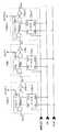
そのため、駆動回路一体型液晶表示装置では、水平スキャナを構成するシフトレジスタとして、レベルシフト機能を持つシフトレジスタを用いていた。このレベルシフト機能付きシフトレジスタの従来例を図8に示す。ここでは、n段目の転送段(レジスタ段)の構成を例にとって説明するが、他の転送段も全く同じ構成となっている。
【0005】
前段(n−1段)から供給される転送パルスQn−1は、Dタイプフリップフロップ(以下、単にD-FFと記す)101nに対してそのD入力として与えられるとともに、ANDゲート102nおよびORゲート103nに対してそれらの各一方の入力として与えられる。D-FF101nのQ出力は、バッファ104nを介して転送パルスQnとして次段(n+1段)に供給されるとともに、ANDゲート102nおよびORゲート103nに対してそれらの各他方の入力として与えられる。
【0006】
ANDゲート102nの出力パルスは自段の水平走査パルスOUTnとなる。ORゲート103nの出力は、レベルシフタ105nに対してこれをレベルシフト動作可能な状態とさせるためのON制御パルスとして与えられる。レベルシフタ105nには、アクティブLow(低レベルがアクティブ)のリセットパルスXRESETが与えられるとともに、互いに逆相のクロックCK,XCKが与えられる。これらクロックCK,XCKは、低電圧振幅の水平クロックHck(同相のクロックおよび逆相のクロック)である。
【0007】
レベルシフタ105nは、ORゲート103nからON制御パルスが与えられることでレベルシフト動作可能な状態となり、低電圧振幅の水平クロックHckであるクロックCK,XCKを高電圧振幅のクロックにレベル変換(レベルシフト)してD-FF101nに対してそのクロック(CK)入力として与える。n段目では、クロックCKについてレベルシフト動作が行われる。
【0008】
次に、上記構成の従来例に係るレベルシフト機能付きシフトレジスタの回路動作について、図9のタイミングチャートを用いてn段目の回路動作を中心に説明する。なお、図9のタイミングチャートには、n−1段目〜n+1段目の各部の信号のタイミング関係が示されている。
【0009】
n−1段目から転送パルスQn−1が入力され、これがORゲート103を通してレベルシフタ105nにON制御パルスとして与えられることにより、レベルシフタ105nはレベルシフト動作可能な状態となり、低電圧振幅のクロックCK,XCKを高電圧振幅のクロックにレベル変換する。このレベル変換されたクロックCKはD-FF101nにそのCK入力として与えられる。
【0010】
転送パルスQn−1は同時に、D-FF101nに対してそのD入力として与えられる。すると、D-FF101nのQ出力FFnがクロックCKの立ち上がりのタイミングで低レベル(以下、“L”レベルと記す)から高レベル(以下、“H”レベルと記す)に遷移する。このD-FF101nのQ出力FFnがORゲート103を通してレベルシフタ105nにON制御パルスとして与えられることで、レベルシフタ105nは引き続きレベルシフト動作可能な状態を維持して、クロックCK,XCKに対するレベル変換動作を続ける。
【0011】
D-FF101nのQ出力FFnはさらに、バッファ104nを経由して自段の転送パルスQnとしてn+1段目に供給されるとともに、ANDゲート102nにも供給される。ANDゲート102nでは、前段からの転送パルスQn−1とD-FF101nのQ出力FFnとの論理積演算が行われる。そして、このANDゲート102nの論理積出力が、自段の水平走査パルスOUTnとして出力されることになる。
【0012】
【発明が解決しようとする課題】
ところで、パルスを順次転送するシフトレジスタにおいて、各転送段間で転送パルスを伝送する配線には、図10の等価回路図に示すように、抵抗や容量などの寄生素子が少なからず存在し、この寄生素子の影響によって転送パルスに遅延が生じるのは避けられない問題である。この遅延は、ANDゲート102nを通して水平走査パルスOUTnの遅延の原因となって現れる。
【0013】
特に、上述した従来例に係るシフトレジスタでは、転送パルスQn−1のパルス幅をクロックCKの1周期とし、この転送パルスQn−1をD-FF101nでラッチし、そのラッチ出力パルスと転送パルスQn−1との論理積をANDゲート102nでとって水平走査パルスOUTnとして出力する構成を採っていることから、D-FF101nでの遅延も発生し、その遅延時間も加わることになるため、クロックCK,XCKのパルスエッジから水平走査パルスOUTnの出力までの応答時間が長くなるという課題があった。さらに、D-FF101nの存在によってその分だけ回路規模が増大するとともに、消費電力も増加するという課題があった。
【0014】
本発明は、上記課題に鑑みてなされたものであり、その目的とするところは、クロックに対するシフトパルスの出力の応答性に優れるとともに、回路規模の縮小化および低消費電力化を可能にしたレベルシフト機能付きシフトレジスタおよびこれを用いた表示装置、ならびに当該表示装置を具備するカメラシステムおよび携帯端末装置を提供することにある。
【0015】
【課題を解決するための手段】
本発明によるシフトレジスタは、縦続接続された転送段の各々が、前段から供給される転送パルスを一方の入力とするORゲートと、このORゲートの出力信号に応答して動作状態となってクロック信号のレベルをシフトするレベルシフタと、ORゲートの出力信号とレベルシフタでレベルシフトされたクロック信号との論理積をとり、その出力信号を自段のシフトパルスおよび次段への転送パルスとして出力するとともに、ORゲートに対してその他方の入力として与えるANDゲートとを有する構成となっている。
【0016】
上記構成のレベルシフタ機能付きシフトレジスタにおいて、ORゲートは前段から供給される転送パルスと自段のシフトパルスとの論理和をとり、レベルシフタにレベルシフト動作可能な状態とする制御信号として与える。レベルシフタはこれに応答してクロック信号のレベルシフト動作を行い、そのレベルシフト後のクロック信号をANDゲートに与える。すると、ANDゲートは、ORゲートの出力信号とレベルシフト後のクロック信号との論理積をとり、自段のシフトパルスおよび次段への転送パルスとして出力する。このレベルシフタ機能付きシフトレジスタは、表示装置の走査系を構成するシフトレジスタとして用いられる。そして、この表示装置は、カメラシステムや携帯端末装置において、その表示装置として搭載される。
【0017】
【発明の実施の形態】
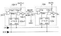
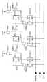
以下、本発明の実施の形態について図面を参照して詳細に説明する。図1は、本発明の一実施形態に係るレベルシフト機能付きシフトレジスタの構成を示すブロック図である。ここでは、図面の簡略化のために、n−1段目、n段目、n+1段目の各転送段10n−1,10n,10n+1のみを示している。また、縦続接続された各転送段は同じ構成となっているので、n段目の転送段10nの場合を例にとってその具体的な構成について説明するものとする。
【0018】
図1において、n段目の転送段10nは、2入力ORゲート11n、レベルシフタ12n、2入力ANDゲート13nおよびバッファ14nを有する構成となっている。ORゲート11nは、n−1段目から供給される転送パルスQn−1を一方の入力とし、ANDゲート13nの出力を他方の入力としている。ORゲート11nの論理和信号ENnは、レベルシフタ12nに対してそのON制御信号、即ちレベルシフト動作可能な状態とするための制御信号として与えられるとともに、ANDゲート13nに対してその一方の入力として与えられる。
【0019】
レベルシフタ12nにはアクティブLowのリセットパルスXRESETが与えられるとともに、例えば低電圧振幅の互いに逆相のクロックCK,XCKが与えられる。レベルシフタ12nは、ORゲート11nからON制御信号が与えられることによってレベルシフト動作可能な状態となり、低電圧振幅のクロックCK,XCKを高電圧振幅のクロックCK,XCKにレベルシフト(レベル変換)する。
【0020】
ここで、レベルシフタに対する低電圧振幅のクロックCK,XCKの入力については、各段ごとに交互に正相、逆相の繰り返しで入力される。すなわち、レベルシフタ12nにはクロックCK,XCKがCK入力、XCK入力として与えられ、レベルシフタ12n−1,12n+1にはクロックCK,XCKがXCK入力、CK入力として与えられる。したがって、本段(n段)ではレベル変換後のクロックCKが、ANDゲート13nに対してその他方の入力として与えられることになる。
【0021】
ANDゲート13nの論理積信号は、自段のシフトパルスOUTnとして出力されるとともに、ORゲート11nに対してその他方の入力として与えられ、さらにバッファ14nを経由して自段の転送パルスQnとして次段(n+1段)の転送段10n+1に供給される。
【0022】
以下、上記構成の本実施形態に係るレベルシフト機能付きシフトレジスタの回路動作について、図2のタイミングチャートを用いてn段目を中心に説明する。なお、図2のタイミングチャートには、n−1段目〜n+1段目の各部の信号のタイミング関係が示されている。
【0023】
n−1段目の転送段10n−1から出力される転送パルスQn−1がn段目の転送段10nに供給される。ここで、図3の等価回路に示すように、n−1段目の転送段10n−1からn段目の転送段10nに転送パルスQn−1を伝送する配線には抵抗や容量などの寄生素子が少なからず存在し、その影響を受けることによって転送パルスQn−1は、n−1段目のシフトパルスOUTn−1に対して若干の遅れ(遅延時間Td)をもってn段目の転送段10nに供給される。
【0024】
転送パルスQn−1がn段目の転送段10nに入力されると、ORゲート11nの論理和信号ENnが“H”レベルとなり、レベルシフタ12nにそのON制御信号として与えられるとともに、ANDゲート13nに一方の入力として与えられる。これにより、レベルシフタ12nが動作状態、即ちレベルシフト動作が可能な状態となる。
【0025】
そして、クロックCK,XCKが“H”レベルになると、レベルシフタ12nにおいて、低電圧振幅のクロックCK,XCKを高電圧振幅のクロックCK,XCKにレベルシフトする動作が行われる。ここで、転送パルスQn−1には先述した配線の寄生素子に起因する遅延があり、クロックCKが“H”レベルに遷移した後に転送パルスQn−1が“L”レベルに遷移するため、クロックCKが立ち上がる前にレベルシフタ12nが非動作状態になることはない。
【0026】
レベルシフタ10nでレベル変換されたクロックCKがANDゲート13nにその他方の入力として与えられると、ANDゲート13nにおいて、ORゲート11nの論理和信号ENn、即ち前段からの転送パルスQn−1とレベル変換後のクロックCKとの論理積がとられ、その論理積信号が自段のシフトパルスOUTnとして出力されるとともに、バッファ14nを経て転送パルスQnとして次段(n+1段)の転送段10n+1に供給される。
【0027】
ANDゲート13nの論理積信号はさらに、ORゲート11nを通して論理和信号ENnとなり、レベルシフタ12nにそのON制御信号として、ANDゲート13nにその一方の入力として与えられる。これにより、レベルシフタ12nは引き続き動作状態を維持して、クロックCK,XCKに対するレベル変換動作を続ける。
【0028】
次に、クロックCKが“H”レベルから“L”レベルに遷移すると、ANDゲート13nの論理積信号、即ちシフトパルスOUTnが“L”レベルとなり、ORゲート11nの論理和信号ENnも“L”レベルとなるので、レベルシフタ12nが非動作状態、即ちクロックCK,XCKのレベルシフト動作が不可能な状態となる。その結果、ANDゲート13nからはクロックCKと同じパルス幅、即ちクロックCKの半周期のパルス幅のパルス信号が、自段のシフトパルスOUTnとして出力されるとともに、自段の転送パルスQnとしてバッファ14nを経由して次段(n+1段)の転送段10n+1に供給される。
【0029】
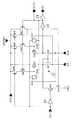
図4は、上記実施形態に係るレベルシフト機能付きシフトレジスタにおいて、n段目の転送段10nを実現するための具体的な回路構成の一例を示す回路図である。
【0030】
図4において、NチャンネルMOSトランジスタQn1,Qn2は、ゲートが相互に接続されかつMOSトランジスタQn1がゲートとドレインが共通接続されたダイオード接続となっていることで、カレントミラー回路21を構成している。MOSトランジスタQn1,Qn2の各ソースには、低電圧振幅の逆相のクロックCK,XCKがそれぞれ入力される。
【0031】
このカレントミラー回路21において、MOSトランジスタQn2のドレイン出力が、インバータ22で反転されて自段のシフトパルスOUTnとして出力されるとともに、バッファ23(図1のバッファ14nに相当)を経由して自段の転送パルスQnとしてn+1段目の転送段10n+1に供給される。
【0032】
MOSトランジスタQn1,Qn2の各ドレインと電源VDDとの間には、PチャンネルMOSトランジスタQp1,Qp2がそれぞれ接続されている。MOSトランジスタQn1のドレインとGNDとの間には、NチャンネルMOSトランジスタQn3,Qn4が直列に接続されている。MOSトランジスタQn3のゲートには、前段からの転送パルスQn−1がインバータ24で反転されて与えられる。MOSトランジスタQn4のゲートには、MOSトランジスタQn2のドレイン出力が直接与えられる。
【0033】
MOSトランジスタQp1のゲートで電源VDDとの間には、PチャンネルMOSトランジスタQp3,Qp4が直列に接続されている。MOSトランジスタQp2のゲートで電源VDDとの間には、PチャンネルMOSトランジスタQp5,Qp6が直列に接続されている。MOSトランジスタQn2のドレイン(MOSトランジスタQp2のドレイン)と電源VDDとの間には、PチャンネルMOSトランジスタQp7,Qp8が並列に接続されている。
【0034】
MOSトランジスタQp3,Qp5,Qp7の各ゲートには、MOSトランジスタQn2のドレイン出力がインバータ22で反転されて与えられる。MOSトランジスタQp4,Qp6の各ゲートには、前段からの転送パルスQn−1が直接与えられる。MOSトランジスタQp8のゲートには、アクティブLowのリセットパルスXRESETが与えられる。
【0035】
MOSトランジスタQp1のゲートには、互いに並列に接続されたNチャンネルMOSトランジスタQn5,Qn6を介してクロックXCKが与えられる。MOSトランジスタQp2のゲートには、互いに並列に接続されたNチャンネルMOSトランジスタQn7,Qn8を介してクロックCKが与えられる。MOSトランジスタQn5,Qn7の各ゲートには、前段からの転送パルスQn−1が直接与えられる。MOSトランジスタQn6,Qn8の各ゲートには、MOSトランジスタQn2のドレイン出力がインバータ22で反転されて与えられる。
【0036】
次に、上記構成の転送部10nのリセット時、休止時、スタンバイ時およびレベルシフト動作時の各回路動作について説明する。
【0037】
(1)リセット時
リセット時、リセットパルスXRESETが“L”レベルになるので、MOSトランジスタQp8がオン状態となる。すると、インバータ22の入力が“H”レベルになるため、その出力OUTnは“L”レベルに固定される。このときまだ、前段から転送パルスQn−1が供給されておらず、インバータ24の出力が“H”レベルの状態にあり、またMOSトランジスタQp8がオンすることでMOSトランジスタQn4のゲートが“H”レベルとなるため、MOSトランジスタQn3,Qn4が共にオン状態となる。
【0038】
MOSトランジスタQn3,Qn4がオンすると、カレントミラー回路21のMOSトランジスタQn1,Qn2の各ゲートが“L”レベルとなるため、これらMOSトランジスタQn1,Qn2はオフ状態となる。さらに、MOSトランジスタQn5,Qn6,Qn7,Qn8がオフ状態となり、MOSトランジスタQp3,Qp4,Qp5,Qp6がオン状態となるため、MOSトランジスタQp1,Qp2のゲートが“H”レベルとなり、MOSトランジスタQp1,Qp2はオフ状態となる。故に、リセット時には、MOSトランジスタQn1,Qn2およびMOSトランジスタQp1,Qp2には電流は流れない。
【0039】
(2)休止時
リセットパルスXRESETが“H”レベルになり、MOSトランジスタQp8がオフ状態となるが、インバータ22の出力OUTnが“L”レベルにあることによってMOSトランジスタQp7がオン状態にあるため、インバータ22の入力が“H”レベルの状態を維持し、したがって出力OUTnは“L”レベルに保持される。
【0040】
リセット時と同様に、MOSトランジスタQn3,Qn4がオンするため、MOSトランジスタQn1,Qn2は各ゲートが“L”レベルとなり、したがってオフ状態となる。さらに、MOSトランジスタQn5〜Qn8がオフ、MOSトランジスタQp3〜Qp6がオンするため、MOSトランジスタQp1,Qp2のゲートが“H”レベルとなり、MOSトランジスタQp1,Qp2はオフ状態となる。故に、休止時にも、MOSトランジスタQn1,Qn2およびMOSトランジスタQp1,Qp2には電流が流れない。
【0041】
(3)スタンバイ時
前段から“H”レベルの転送パルスQn−1が入力されると、MOSトランジスタQn3,Qp4,Qp6がオフ状態となり、MOSトランジスタQn5,Qn7がオン状態となるため、MOSトランジスタQp1,Qp2およびMOSトランジスタQn1,Qn2のオフ状態が解除される。また、クロックCK,XCKの低電圧振幅を0V〜Vppとすると、クロックCKの電圧が0V、クロックXCKの電圧がVppである。
【0042】
このとき、MOSトランジスタQp1,Qp2,Qn1,Qn2の各ゲート-ソース間電圧をVgs(p1),Vgs(p2),Vgs(n1),Vgs(n2)とすると、それらの関係は、
Vgs(p1)<Vgs(p2)
Vgs(n1)>Vgs(n2)
となる。
【0043】
仮に、MOSトランジスタQp1,Qp2およびMOSトランジスタQn1,Qn2のサイズ比が1対1ならば、MOSトランジスタQp1,Qp2,Qn1,Qn2に流れようとする電流をI(p1),I(p2),I(n1),I(n2)とすると、それらの関係は、
I(p2)>I(p1)=I(n1)>I(n2)
となる。よって、MOSトランジスタQp2,Qn2の各ドレイン電圧は“H”レベルに保持される。
【0044】
(4)レベルシフト動作時
クロックCKの電圧がVpp、クロックXCKの電圧が0Vとなると、Vgs(p1),Vgs(p2),Vgs(n1),Vgs(n2)の関係は、
Vgs(p1)>Vgs(p2)
Vgs(n1)<Vgs(n2)
となる。
【0045】
仮に、MOSトランジスタQp1,Qp2およびMOSトランジスタQn1,Qn2のサイズ比が1対1ならば、I(p1),I(p2),I(n1),I(n2)の関係は、
I(p2)<I(p1)=I(n1)<I(n2)
となる。したがって、MOSトランジスタQp2,Qn2の各ドレイン電圧はほぼ“L”レベルになる。そして、このドレイン電圧はインバータ22によって反転され、VDDレベルである“H”レベルにレベルシフトされる。
【0046】
この後、転送パルスQn−1が“L”レベルになって、MOSトランジスタQn4,Qn5,Qn7,Qp3,Qp5がオフしても、MOSトランジスタQn6,Qn8がオンするので、MOSトランジスタQp1,Qp2およびMOSトランジスタQn1,Qn2がオフ状態になることはない。
【0047】
次に、クロックCKの電圧が0V、クロックXCKの電圧がVppとなると、Vgs(p1),Vgs(p2),Vgs(n1),Vgs(n2)の関係は、
Vgs(p1)<Vgs(p2)
Vgs(n1)>Vgs(n2)
となる。
【0048】
仮に、MOSトランジスタQp1,Qp2およびMOSトランジスタQn1,Qn2のサイズ比が1対1ならば、I(p1),I(p2),I(n1),I(n2)の関係は、
I(p2)>I(p1)=I(n1)>I(n2)
となる。よって、MOSトランジスタQp2,Qn2の各ドレイン電圧は“H”レベルになる。そして、このドレイン電圧はインバータ22によって反転され、“L”レベルにレベルシフトされる(OUTn)。
【0049】
すると、MOSトランジスタQn3,Qn4がオンするので、MOSトランジスタQn1,Qn2の各ゲート電位が“L”レベルとなり、これらMOSトランジスタQn1,Qn2はオフ状態になる。さらに、MOSトランジスタQn5,Qn6,Qn7,Qn8がオフし、MOSトランジスタQp3,Qp4,Qp5,Qp6がオンするので、MOSトランジスタQp1,Qp2の各ゲート電位が“H”レベルとなり、これらMOSトランジスタQp1,Qp2もオフする。
【0050】
しかし、MOSトランジスタQp7がオンすることにより、MOSトランジスタQp2,Qn2の各ドレイン電位が確実に“H”レベルになり、また出力OUTnは“L”レベルで保持される。ここで、再び、上述した休止状態(2)となり、上述した回路動作が繰り返される。
【0051】
上述した回路構成のレベルシフト機能付きシフトレジスタは、同じ導電型MOSトランジスタQp1とQp2およびQn1とQn2のマッチングのみが重要であり、異なる導電型であるMOSトランジスタQp1とQn1およびQp2とQn2のマッチングはレベルシフト動作マージンにさほど影響を与えないので、薄膜トランジスタを使用した製造ばらつきの大きいプロセスに対して動作マージンが大である。また、MOSトランジスタQn1,Qn2からなるカレントミラー回路21のカレントミラー比をクロックCK,XCKの反転ごとに積極的に変化させることにより、ダイナミック応答の向上も可能である。
【0052】
以上のように、本実施形態に係るレベルシフト機能付きシフトレジスタにおいては、転送パルスのパルス幅をクロックCKの半周期とするとともに、各転送段間で転送パルスを伝送する配線に存在する抵抗や容量などの寄生素子の影響によって転送パルスに生じる遅延を積極的に利用し、ORゲート11nを経た転送パルスQn−1とレベルシフト後のクロックCKとの論理積をANDゲート13nでとってシフトパルスOUTnとして出力するとともに、その論理積出力をORゲート11nに帰還することで、従来技術では、回路規模の小型化や低消費電力化の妨げとなっていたD-FFを必要としない回路構成を実現している。
【0053】
換言すれば、転送段の各々を、ORゲート、レベルシフタ、ANDゲートおよびバッファ、具体的な回路例の一つとして、各々8個のPチャンネルMOSトランジスタQp1〜Qp8,Qn1〜Qn8、2個のインバータ22,24およびバッファ23の簡単な回路構成によって実現できるので、各転送段ごとにD-FFを不要とする分だけ、シフトレジスタ全体の回路規模の小型化および低消費電力化が図れる。
【0054】
また、ANDゲート13nの出力パルスを直接シフトパルスOUTnとして導出するとともに、転送パルスQnとしてバッファ14nを経由して次段の転送段10n+1に供給する構成を採っていることで、転送パルスQnの伝送系とシフトパルスOUTnの出力系とがバッファ14nによって分断され、しかも従来技術のように、シフトパルスOUTnとして導出する際に前段の転送パルスQn−1との論理積をとっていないため、クロックCKに対するシフトパルスOUTnの出力応答が、前段からの転送パルスの遅延の影響を受けず、かつ、必要なときにn段目だけクロックCKのレベルシフタ12nを動作させながら、シフト動作を繰り返すことができる。
【0055】
[適用例]
以上説明したレベルシフト機能付きシフトレジスタは、表示装置、例えば画素の電気光学素子として液晶セルを用いた液晶表示装置やエレクトロルミネッセンス(EL)素子を用いたEL表示装置の走査系を構成するシフトレジスタや、MOS型などに代表されるX-Yアドレス型固体撮像装置の走査系を構成するシフトレジスタなどに適用可能である。
【0056】
但し、本発明はこれらの適用例に限定されるものではなく、レベルシフト機能を持つシフトレジスタ全般に適用し得るものである。ここでは、一例として、液晶表示装置の水平駆動系を構成するシフトレジスタに適用した場合を例にとって説明する。
【0057】
図5は、駆動回路一体型液晶表示装置の構成例を示す概略構成図である。本液晶表示装置では、その駆動方式として、画素の各々に対して個々の独立した画素電極を配列し、これら画素電極の各々に薄膜トランジスタ(TFT;Thin Film Transistor)などのスイッチング素子を接続して画素を選択的に駆動する、いわゆるアクティブマトリクス駆動方式(以下、アクティブマトリクス型と記す)を用いている。
【0058】
図5において、本例に係るアクティブマトリクス型液晶表示装置は、後述するように画素が行列状(マトリクス状)に配置されてなる画素部31と、画素部31の例えば上側に配置され、各画素への映像信号の書き込みを例えば点順次で行う水平(H)駆動系32と、画素部31の例えば左側に配置され、各画素を行単位で選択する垂直(V)駆動系33とを備え、水平駆動系32および垂直駆動系33が画素部31と共に、例えばTFTを用いて同一の基板(液晶パネル)34上に一体的に形成された構成となっている。
【0059】
画素部31は、スイッチング素子として例えばTFT(画素トランジスタ)が形成されたTFT基板と、カラーフィルタや対向電極等が形成された対向基板とを重ね合わせ、これら2枚の透明絶縁基板(例えば、ガラス基板)間に液晶材料を封入することによって作製される。この画素部31において、行列状に配置された各画素40は、スイッチング素子であるTFT41と、このTFT41のドレイン電極に画素電極が接続された液晶セル42と、TFT41のドレイン電極に一方の電極が接続された補助キャパシタ43とから構成されている。
【0060】
この画素構造において、各画素40のTFT41は、そのゲート電極が垂直方向(行方向)の画素数Y(以下、垂直画素数Yと称す)に対応したy行分のゲートライン44-1,44-2,……,44-y-1,44-yの各々にそれぞれ接続され、かつそのソース電極が水平方向(列方向)の画素数X(以下、水平画素数Xと称す)に対応したx列分の信号ライン45-1,45-2,……,45-x-1,45-xの各々にそれぞれ接続されている。また、液晶セル42の対向電極および補助キャパシタ43の他方の電極は、コモン電位Vcomが与えられるコモンライン46に接続されている。
【0061】
水平駆動系32は、水平画素数Xに対応した段数のシフトレジスタからなるHスキャナ321と、水平画素数Xに対応して設けられたx個の水平スイッチ322-1〜322-xとを有する構成となっている。Hスキャナ321はシフトレジスタによって構成され、水平スタートパルスHstを水平クロックHckに同期して順に転送することによって得られる各段の転送パルスを水平走査パルスとして順に出力する。このHスキャナ321を構成するシフトレジスタとして、先述した実施形態に係るレベルシフト機能付きシフトレジスタが用いられる。
【0062】
Hスキャナ321には、外部から供給される例えばTTLレベルの低電圧振幅の水平スタートパルスHstが、液晶パネル34上に作製されたレベル変換回路35によって液晶の駆動に必要な高電圧振幅のパルスに変換されて入力される。水平クロックHckについては、外部から供給される例えばTTLレベルの低電圧振幅のままHスキャナ321に入力され、先述したシフトレジスタ内のレベルシフタで高電圧振幅のクロックに変換される。
【0063】
水平スイッチ322-1〜322-xは例えばMOSトランジスタからなり、Hスキャナ321から順に出力される水平走査パルスに応答して順にオン状態となることで、映像信号を画素部31の信号ライン45-1〜45-xに順次供給する。
【0064】
垂直駆動系33は、垂直画素数Yに対応した段数のシフトレジスタからなるVスキャナ331によって構成されている。Vスキャナ331は例えばシフトレジスタによって構成され、垂直スタートパルスVstを垂直クロックVckに同期して順に転送することによって得られる各段の転送パルスを垂直走査パルスとして順に出力する。これら垂直走査パルスは、画素部31のゲートライン44-1〜44-yに順次与えられる。
【0065】
なお、本適用例では、先述した実施形態に係るレベルシフト機能付きシフトレジスタを、Hスキャナ321を構成するシフトレジスタとして用いるとしたが、Vスキャナ331を構成するシフトレジスタとして用いることも可能である。
【0066】
このように、駆動回路一体型液晶表示装置において、例えば水平駆動系のスキャナを構成するシフトレジスタとして、先述したレベルシフト機能付きシフトレジスタを用いることにより、当該シフトレジスタは回路規模の小型化、低消費電力化が可能であるため、液晶パネル34の駆動回路を形成する画素部周辺の領域(額縁)の狭額縁化および液晶表示装置の低消費電力化に大きく寄与できる。特に、レベルシフト機能付きシフトレジスタがTFTを使用した製造ばらつきの大きいプロセスに有効な回路であるため、当該シフトレジスタの適用例としては、駆動系を画素トランジスタと共にTFTを用いて同一基板上に一体形成してなる駆動回路一体型液晶表示装置が最適である。
【0067】
本例に係る駆動回路一体型液晶表示装置は、ビデオカメラやデジタルスチルカメラなどのカメラシステムのモニターとして、あるいは携帯電話機やPDA(Personal Digital Assistants)などの携帯端末装置の表示装置として用いて好適なものである。
【0068】
図6は、本発明に係るカメラシステム、例えばVTR機能を一体的に搭載したカムコーダと称されるビデオカメラの構成例を概略的に示すブロック図である。図6において、撮像デバイス、例えばCCD(Charge Coupled Device)撮像素子51で被写体の撮像が行われ、その撮像信号はアナログ信号処理回路52およびカメラ信号処理回路53で各種の信号処理が行われる。
【0069】
具体的には、アナログ信号処理回路52では、CCD撮像素子51から出力される撮像信号に対して、当該撮像素子51の出力部で発生する1/fノイズなどを除去するためのCDS(相関二重サンプリング)処理や、信号レベルを一定にするためのAGC(自動利得制御)処理などの信号処理が行われる。また、カメラ信号処理回路53では、輝度信号および色差信号の生成や、オートホワイトバランス等の画質調整などの信号処理が例えばデジタル処理にて行われ、最終的にアナログ映像信号として出力される。
【0070】
このアナログ映像信号は、記録/再生部54に供給される。記録/再生部54は、入力されるアナログ映像信号を磁気テープなどの記録媒体55に記録(あるいは、画像メモリなどの記憶媒体に記憶)し、また記録媒体55に記録されている記録情報を再生する。
【0071】
本カムコーダは、撮像中の被写体(撮像画像)を確認するための表示装置として、液晶モニタ56および液晶ビューファインダ57を備えている。これら液晶モニタ56および液晶ビューファインダ57として、先述した実施形態に係る駆動回路一体型液晶表示装置が用いられる。そして、液晶モニタ56および液晶ビューファインダ57には、ドライバIC58でコモン電位Vcomを中心に交流駆動化されたアナログ映像信号が、切り替えスイッチ59を介して選択的に供給される。
【0072】
このように、本発明に係るカメラシステムでは、液晶モニタ56および液晶ビューファインダ57として、先述した実施形態に係る駆動回路一体型液晶表示装置を用いていることにより、当該液晶表示装置は狭額縁化および低消費電力化が可能であるため、本カメラシステムの小型化および低消費電力化に大きく寄与できる。
【0073】
なお、本適用例では、液晶モニタ56および液晶ビューファインダ57の双方に、先述した実施形態に係る駆動回路一体型液晶表示装置を用いるとしたが、いずれか一方のみに用いるようにしても良く、またいずれか一方の液晶表示装置を備えたビデオカメラやデジタルスチルカメラなどのカメラシステムに対しても同様に適用可能である。
【0074】
図7は、本発明に係る携帯端末装置、例えば携帯電話機の構成の概略を示す外観図である。本例に係る携帯電話機は、装置筐体61の前面側に、スピーカ部62、表示部63、操作部64およびマイク部65が上部側から順に配置された構成となっている。かかる構成の携帯電話機において、表示部63には例えば液晶表示装置が用いられ、この液晶表示装置として、先述した実施形態に係る駆動回路一体型液晶表示装置が用いられる。
【0075】
このように、携帯電話機やPDAなどの携帯端末装置において、先述した実施形態に係る駆動回路一体型液晶表示装置を表示部53として用いることにより、当該液晶表示装置は狭額縁化および低消費電力化が可能であるため、本端末装置の小型化および低消費電力化に大きく寄与でき、特に低消費電力化によってバッテリの使用時間を延長できる効果がある。
【0076】
【発明の効果】
以上説明したように、本発明によれば、レベルシフト機能付きシフトレジスタの各転送段を、従来技術では回路規模の小型化や低消費電力化の妨げとなっていたD-FFを必要としない回路構成で実現しているので、回路規模の縮小化および低消費電力化が図れる。
【図面の簡単な説明】
【図1】本発明の一実施形態に係るレベルシフト機能付きシフトレジスタの構成を示すブロック図である。
【図2】本実施形態に係るレベルシフト機能付きシフトレジスタの回路動作を説明するためのタイミングチャートである。
【図3】本実施形態に係るレベルシフト機能付きシフトレジスタの等価回路図である。
【図4】n段目の転送段を実現するための具体的な回路構成例を示す回路図である。
【図5】駆動回路一体型液晶表示装置の構成例を示す概略構成図である。
【図6】本発明に係るカメラシステムの構成例を概略的に示すブロック図である。
【図7】本発明に係る携帯端末装置の構成の概略を示す外観図である。
【図8】従来例に係るレベルシフト機能付きシフトレジスタの構成を示すブロック図である。
【図9】従来例に係るレベルシフト機能付きシフトレジスタの回路動作を説明するためのタイミングチャートである。
【図10】従来例に係るレベルシフト機能付きシフトレジスタの等価回路図である。
【符号の説明】
10n−1〜10n+1…転送段、11n−1〜11n+1…ORゲート、12n−1〜12n+1…レベルシフタ、13n−1〜13n+1…ANDゲート、14n−1〜14n+1…バッファ[0001]
BACKGROUND OF THE INVENTION
The present invention relates to a shift register, a display device using the shift register, a camera system, and a portable terminal device, and more particularly, to a shift register having a level shift function, a display device using the shift register, and a camera system and a portable device including the display device. It relates to a terminal device.
[0002]
[Prior art]
As a display device, for example, a liquid crystal display device, a so-called drive circuit in which a drive circuit for driving a pixel portion in which pixels are arranged in a matrix is integrally formed on the same substrate (liquid crystal panel) as the pixel portion. There is an integrated liquid crystal display device. In this driving circuit integrated liquid crystal display device, for example, a low voltage amplitude level of a TTL signal is supplied from an external IC into the liquid crystal panel. Therefore, this low voltage amplitude level is set to a high level necessary for driving the liquid crystal in the liquid crystal panel. It needs to be converted to a voltage amplitude level.
[0003]
As an example, considering a horizontal drive system, conventionally, the horizontal start pulse Hst applied from the outside is converted into a high voltage amplitude level by a level conversion circuit provided in the liquid crystal panel and supplied to the horizontal scanner. The horizontal clock Hck supplied from the outside is supplied to the horizontal scanner as it is at the low voltage amplitude level, and is converted to the high voltage amplitude level by the level shifter built in the shift register constituting the horizontal scanner. .
[0004]
Therefore, in the drive circuit integrated liquid crystal display device, a shift register having a level shift function is used as a shift register constituting the horizontal scanner. A conventional example of a shift register with a level shift function is shown in FIG. Here, the configuration of the nth transfer stage (register stage) will be described as an example, but the other transfer stages have the same configuration.
[0005]
The transfer pulse Qn-1 supplied from the previous stage (n-1 stage) is given as its D input to a D-type flip-flop (hereinafter simply referred to as D-FF) 101n, and also includes an
[0006]
The output pulse of the
[0007]
The level shifter 105n is in a state in which a level shift operation is possible when an ON control pulse is applied from the
[0008]
Next, the circuit operation of the shift register with level shift function according to the conventional example having the above configuration will be described with a focus on the n-th stage circuit operation with reference to the timing chart of FIG. Note that the timing chart of FIG. 9 shows the timing relationship of the signals of the respective sections from the (n−1) th stage to the (n + 1) th stage.
[0009]
The transfer pulse Qn−1 is input from the (n−1) th stage, and this is given as an ON control pulse to the level shifter 105n through the OR gate 103, whereby the level shifter 105n becomes ready for level shift operation, and the low voltage amplitude clocks CK, XCK is level-converted to a clock having a high voltage amplitude. This level-converted clock CK is given to the D-FF 101n as its CK input.
[0010]
The transfer pulse Qn-1 is simultaneously given as its D input to the D-FF 101n. Then, the Q output FFn of the D-
[0011]
The Q output FFn of the D-
[0012]
[Problems to be solved by the invention]
By the way, in the shift register for sequentially transferring pulses, there are not a few parasitic elements such as resistors and capacitors in the wiring for transmitting the transfer pulses between the transfer stages, as shown in the equivalent circuit diagram of FIG. It is an unavoidable problem that the transfer pulse is delayed due to the influence of the parasitic element. This delay appears as a cause of the delay of the horizontal scanning pulse OUTn through the
[0013]
In particular, in the shift register according to the above-described conventional example, the pulse width of the transfer pulse Qn-1 is set to one cycle of the clock CK, the transfer pulse Qn-1 is latched by the D-
[0014]
The present invention has been made in view of the above problems, and the object of the present invention is to provide a level that is excellent in the response of the output of the shift pulse with respect to the clock, and that can reduce the circuit scale and reduce the power consumption. It is an object of the present invention to provide a shift register with a shift function, a display device using the shift register, a camera system and a portable terminal device including the display device.
[0015]
[Means for Solving the Problems]
In the shift register according to the present invention, each of the cascade-connected transfer stages has an OR gate that receives the transfer pulse supplied from the previous stage as one input and an operating state in response to an output signal of the OR gate. The logical product of the level shifter that shifts the level of the signal and the output signal of the OR gate and the clock signal level-shifted by the level shifter is output, and the output signal is output as a shift pulse of the own stage and a transfer pulse to the next stage. , And an AND gate given as the other input to the OR gate.
[0016]
In the shift register with the level shifter function configured as described above, the OR gate takes the logical sum of the transfer pulse supplied from the previous stage and the shift pulse of the own stage, and gives it to the level shifter as a control signal for enabling the level shift operation. In response to this, the level shifter performs a level shift operation of the clock signal, and applies the clock signal after the level shift to the AND gate. Then, the AND gate takes a logical product of the output signal of the OR gate and the clock signal after the level shift, and outputs it as a shift pulse of its own stage and a transfer pulse to the next stage. This shift register with a level shifter function is used as a shift register constituting a scanning system of a display device. And this display apparatus is mounted as the display apparatus in a camera system or a portable terminal device.
[0017]
DETAILED DESCRIPTION OF THE INVENTION
Hereinafter, embodiments of the present invention will be described in detail with reference to the drawings. FIG. 1 is a block diagram showing a configuration of a shift register with a level shift function according to an embodiment of the present invention. Here, for simplification of the drawing, only the transfer stages 10n-1, 10n, 10n + 1 of the (n-1) th stage, the nth stage, and the (n + 1) th stage are shown. Since the cascaded transfer stages have the same configuration, the specific configuration will be described by taking the case of the n-
[0018]
In FIG. 1, the n-
[0019]
The
[0020]
Here, the low-voltage amplitude clocks CK and XCK are input to the level shifter alternately in the normal phase and the reverse phase for each stage. That is, the clocks CK and XCK are supplied to the
[0021]
The AND signal of the AND
[0022]
Hereinafter, the circuit operation of the shift register with level shift function according to the present embodiment having the above-described configuration will be described with a focus on the nth stage using the timing chart of FIG. Note that the timing chart of FIG. 2 shows the timing relationship of the signals of the respective sections from the (n−1) th stage to the (n + 1) th stage.
[0023]
The transfer pulse Qn-1 output from the (n-1)
[0024]
When the transfer pulse Qn-1 is input to the n-
[0025]
When the clocks CK and XCK become “H” level, the
[0026]
When the clock CK level-converted by the
[0027]
The logical product signal of the AND
[0028]
Next, when the clock CK transitions from the “H” level to the “L” level, the logical product signal of the AND
[0029]
FIG. 4 is a circuit diagram showing an example of a specific circuit configuration for realizing the n-
[0030]
In FIG. 4, N-channel MOS transistors Qn1 and Qn2 form a
[0031]
In the
[0032]
P-channel MOS transistors Qp1 and Qp2 are connected between the drains of the MOS transistors Qn1 and Qn2 and the power supply VDD, respectively. N-channel MOS transistors Qn3 and Qn4 are connected in series between the drain of the MOS transistor Qn1 and GND. Transfer pulse Qn-1 from the previous stage is inverted by
[0033]
P-channel MOS transistors Qp3 and Qp4 are connected in series between the gate of the MOS transistor Qp1 and the power supply VDD. P-channel MOS transistors Qp5 and Qp6 are connected in series between the gate of the MOS transistor Qp2 and the power supply VDD. P-channel MOS transistors Qp7 and Qp8 are connected in parallel between the drain of the MOS transistor Qn2 (the drain of the MOS transistor Qp2) and the power supply VDD.
[0034]
The drain output of the MOS transistor Qn2 is inverted by the
[0035]
A clock XCK is applied to the gate of the MOS transistor Qp1 through N-channel MOS transistors Qn5 and Qn6 connected in parallel. A clock CK is applied to the gate of the MOS transistor Qp2 via N-channel MOS transistors Qn7 and Qn8 connected in parallel. Transfer pulse Qn-1 from the previous stage is directly applied to the gates of MOS transistors Qn5 and Qn7. The drain output of the MOS transistor Qn2 is inverted by the
[0036]
Next, each circuit operation at the time of resetting, resting, standby, and level shift operation of the
[0037]
(1) At reset
At the time of reset, the reset pulse XRESET is set to the “L” level, so that the MOS transistor Qp8 is turned on. Then, since the input of the
[0038]
When the MOS transistors Qn3 and Qn4 are turned on, the gates of the MOS transistors Qn1 and Qn2 of the
[0039]
(2) At rest
The reset pulse XRESET is set to “H” level, and the MOS transistor Qp8 is turned off. However, since the output OUTn of the
[0040]
Since the MOS transistors Qn3 and Qn4 are turned on in the same manner as at the time of resetting, the gates of the MOS transistors Qn1 and Qn2 are set to the “L” level, and thus are turned off. Further, since the MOS transistors Qn5 to Qn8 are turned off and the MOS transistors Qp3 to Qp6 are turned on, the gates of the MOS transistors Qp1 and Qp2 are set to the “H” level, and the MOS transistors Qp1 and Qp2 are turned off. Therefore, no current flows through the MOS transistors Qn1 and Qn2 and the MOS transistors Qp1 and Qp2 even during a pause.
[0041]
(3) During standby
When "H" level transfer pulse Qn-1 is input from the previous stage, MOS transistors Qn3, Qp4 and Qp6 are turned off and MOS transistors Qn5 and Qn7 are turned on. Therefore, MOS transistors Qp1 and Qp2 and MOS transistor The off states of Qn1 and Qn2 are released. When the low voltage amplitude of the clocks CK and XCK is 0 V to Vpp, the voltage of the clock CK is 0 V and the voltage of the clock XCK is Vpp.
[0042]
At this time, assuming that the gate-source voltages of the MOS transistors Qp1, Qp2, Qn1, and Qn2 are Vgs (p1), Vgs (p2), Vgs (n1), and Vgs (n2), their relationship is
Vgs (p1) <Vgs (p2)
Vgs (n1)> Vgs (n2)
It becomes.
[0043]
If the size ratio of the MOS transistors Qp1 and Qp2 and the MOS transistors Qn1 and Qn2 is 1: 1, currents that flow through the MOS transistors Qp1, Qp2, Qn1, and Qn2 are I (p1), I (p2), I Assuming (n1) and I (n2), their relationship is
I (p2)> I (p1) = I (n1)> I (n2)
It becomes. Therefore, the drain voltages of the MOS transistors Qp2 and Qn2 are held at the “H” level.
[0044]
(4) During level shift operation
When the voltage of the clock CK is Vpp and the voltage of the clock XCK is 0 V, the relationship between Vgs (p1), Vgs (p2), Vgs (n1), and Vgs (n2) is
Vgs (p1)> Vgs (p2)
Vgs (n1) <Vgs (n2)
It becomes.
[0045]
If the size ratio of the MOS transistors Qp1 and Qp2 and the MOS transistors Qn1 and Qn2 is 1: 1, the relationship between I (p1), I (p2), I (n1), and I (n2) is
I (p2) <I (p1) = I (n1) <I (n2)
It becomes. Therefore, the drain voltages of the MOS transistors Qp2 and Qn2 are substantially at the “L” level. The drain voltage is inverted by the
[0046]
After this, even if the transfer pulse Qn-1 becomes "L" level and the MOS transistors Qn4, Qn5, Qn7, Qp3, Qp5 are turned off, the MOS transistors Qn6, Qn8 are turned on. MOS transistors Qn1 and Qn2 are not turned off.
[0047]
Next, when the voltage of the clock CK is 0 V and the voltage of the clock XCK is Vpp, the relationship between Vgs (p1), Vgs (p2), Vgs (n1), and Vgs (n2) is
Vgs (p1) <Vgs (p2)
Vgs (n1)> Vgs (n2)
It becomes.
[0048]
If the size ratio of the MOS transistors Qp1 and Qp2 and the MOS transistors Qn1 and Qn2 is 1: 1, the relationship between I (p1), I (p2), I (n1), and I (n2) is
I (p2)> I (p1) = I (n1)> I (n2)
It becomes. Therefore, the drain voltages of the MOS transistors Qp2 and Qn2 are set to the “H” level. The drain voltage is inverted by the
[0049]
Then, since MOS transistors Qn3 and Qn4 are turned on, the gate potentials of MOS transistors Qn1 and Qn2 become "L" level, and these MOS transistors Qn1 and Qn2 are turned off. Further, MOS transistors Qn5, Qn6, Qn7, Qn8 are turned off and MOS transistors Qp3, Qp4, Qp5, Qp6 are turned on, so that the gate potentials of MOS transistors Qp1, Qp2 are set to "H" level, and these MOS transistors Qp1, Qp2 is also turned off.
[0050]
However, when the MOS transistor Qp7 is turned on, the drain potentials of the MOS transistors Qp2 and Qn2 are reliably set to the “H” level, and the output OUTn is held at the “L” level. Here, the above-described rest state (2) is entered again, and the above-described circuit operation is repeated.
[0051]
In the shift register with a level shift function having the above-described circuit configuration, only the matching of the same conductivity type MOS transistors Qp1 and Qp2 and Qn1 and Qn2 is important, and the matching of the MOS transistors Qp1 and Qn1 and Qp2 and Qn2 having different conductivity types is Since the level shift operation margin is not affected so much, the operation margin is large for a process using a thin film transistor and having a large manufacturing variation. Further, the dynamic response can be improved by positively changing the current mirror ratio of the
[0052]
As described above, in the shift register with a level shift function according to the present embodiment, the pulse width of the transfer pulse is set to a half cycle of the clock CK, and the resistance existing in the wiring that transmits the transfer pulse between the transfer stages The delay generated in the transfer pulse due to the influence of the parasitic element such as the capacitance is positively utilized, and the AND of the transfer pulse Qn-1 passed through the
[0053]
In other words, each of the transfer stages includes an OR gate, a level shifter, an AND gate, and a buffer, each of which includes eight P-channel MOS transistors Qp1 to Qp8, Qn1 to Qn8, and two inverters as one specific circuit example. Since it can be realized by a simple circuit configuration of the
[0054]
Further, the output pulse of the AND
[0055]
[Application example]
The shift register with level shift function described above is a shift register that constitutes a scanning system of a display device, for example, a liquid crystal display device using a liquid crystal cell as an electro-optical element of a pixel or an EL display device using an electroluminescence (EL) element. In addition, the present invention can be applied to a shift register constituting a scanning system of an XY address type solid-state imaging device represented by a MOS type.
[0056]
However, the present invention is not limited to these application examples, and can be applied to all shift registers having a level shift function. Here, as an example, a case where the present invention is applied to a shift register constituting a horizontal drive system of a liquid crystal display device will be described as an example.
[0057]
FIG. 5 is a schematic configuration diagram showing a configuration example of a liquid crystal display device integrated with a drive circuit. In this liquid crystal display device, as the driving method, individual pixel electrodes are arranged for each of the pixels, and a switching element such as a thin film transistor (TFT) is connected to each of the pixel electrodes. A so-called active matrix driving method (hereinafter referred to as an active matrix type) is used.
[0058]
5, the active matrix liquid crystal display device according to this example includes a pixel unit 31 in which pixels are arranged in a matrix (matrix shape) as described later, and an upper side of the pixel unit 31, for example. For example, a horizontal (H)
[0059]
The pixel unit 31 includes, for example, a TFT substrate on which a TFT (pixel transistor) is formed as a switching element and a counter substrate on which a color filter, a counter electrode, and the like are formed, and these two transparent insulating substrates (for example, glass) The liquid crystal material is sealed between the substrates. In the pixel unit 31, each pixel 40 arranged in a matrix includes a TFT 41 as a switching element, a liquid crystal cell 42 in which a pixel electrode is connected to the drain electrode of the TFT 41, and one electrode on the drain electrode of the TFT 41. The auxiliary capacitor 43 is connected.
[0060]
In this pixel structure, the TFT 41 of each pixel 40 has gate lines 44-1 and 44 corresponding to y rows whose gate electrodes correspond to the number of pixels Y in the vertical direction (row direction) (hereinafter referred to as the number of vertical pixels Y). -2,..., 44-y-1, 44-y respectively, and the source electrode corresponds to the number of pixels X in the horizontal direction (column direction) (hereinafter referred to as the number of horizontal pixels X). The signal lines 45-1, 45-2,..., 45-x-1, 45-x for x columns are respectively connected. The counter electrode of the liquid crystal cell 42 and the other electrode of the auxiliary capacitor 43 are connected to a
[0061]
The
[0062]
In the
[0063]
The horizontal switches 322-1 to 322-x are composed of, for example, MOS transistors, and are sequentially turned on in response to horizontal scanning pulses sequentially output from the
[0064]
The
[0065]
In this application example, the shift register with a level shift function according to the above-described embodiment is used as a shift register constituting the
[0066]
As described above, in the drive circuit integrated liquid crystal display device, for example, by using the above-described shift register with a level shift function as the shift register constituting the horizontal drive system scanner, the shift register can be reduced in circuit scale and reduced. Since power consumption can be reduced, it can greatly contribute to narrowing the frame (frame) around the pixel portion forming the driving circuit of the liquid crystal panel 34 and reducing power consumption of the liquid crystal display device. In particular, since the shift register with a level shift function is an effective circuit for a process with large manufacturing variations using TFTs, as an application example of the shift register, the drive system is integrated on the same substrate using the TFTs together with the pixel transistors. A liquid crystal display device integrated with a driving circuit is optimal.
[0067]
The drive circuit integrated liquid crystal display device according to this example is suitable for use as a monitor of a camera system such as a video camera or a digital still camera, or as a display device of a mobile terminal device such as a mobile phone or a PDA (Personal Digital Assistants). Is.
[0068]
FIG. 6 is a block diagram schematically showing a configuration example of a camera system according to the present invention, for example, a video camera called a camcorder in which a VTR function is integrally mounted. In FIG. 6, an object is imaged by an imaging device, for example, a CCD (Charge Coupled Device)
[0069]
Specifically, the analog
[0070]
This analog video signal is supplied to the recording / reproducing
[0071]
This camcorder includes a liquid crystal monitor 56 and a
[0072]
As described above, in the camera system according to the present invention, the liquid crystal display device is narrowed by using the drive circuit integrated liquid crystal display device according to the above-described embodiment as the liquid crystal monitor 56 and the
[0073]
In this application example, the liquid crystal monitor 56 and the
[0074]
FIG. 7 is an external view showing an outline of the configuration of a mobile terminal device according to the present invention, for example, a mobile phone. The mobile phone according to the present example has a configuration in which a speaker unit 62, a display unit 63, an operation unit 64, and a microphone unit 65 are arranged in this order from the upper side on the front side of the device casing 61. In the mobile phone having such a configuration, for example, a liquid crystal display device is used as the display unit 63, and the liquid crystal display device according to the above-described embodiment is used as the liquid crystal display device.
[0075]
As described above, in a mobile terminal device such as a mobile phone or a PDA, the liquid crystal display device according to the above-described embodiment is used as the
[0076]
【The invention's effect】
As described above, according to the present invention, each transfer stage of a shift register with a level shift function does not require a D-FF that has hindered circuit size reduction and power consumption reduction in the prior art. Since the circuit configuration is used, the circuit scale can be reduced and the power consumption can be reduced.
[Brief description of the drawings]
FIG. 1 is a block diagram showing a configuration of a shift register with a level shift function according to an embodiment of the present invention.
FIG. 2 is a timing chart for explaining the circuit operation of the shift register with level shift function according to the embodiment.
FIG. 3 is an equivalent circuit diagram of a shift register with a level shift function according to the present embodiment.
FIG. 4 is a circuit diagram illustrating a specific circuit configuration example for realizing an n-th transfer stage.
FIG. 5 is a schematic configuration diagram showing a configuration example of a liquid crystal display device integrated with a drive circuit.
FIG. 6 is a block diagram schematically showing a configuration example of a camera system according to the present invention.
FIG. 7 is an external view schematically showing the configuration of a mobile terminal device according to the present invention.
FIG. 8 is a block diagram showing a configuration of a shift register with a level shift function according to a conventional example.
FIG. 9 is a timing chart for explaining a circuit operation of a shift register with a level shift function according to a conventional example.
FIG. 10 is an equivalent circuit diagram of a shift register with a level shift function according to a conventional example.
[Explanation of symbols]
10n-1 to 10n + 1 ... transfer stage, 11n-1 to 11n + 1 ... OR gate, 12n-1 to 12n + 1 ... level shifter, 13n-1 to 13n + 1 ... AND gate, 14n-1 to 14n + 1 ... buffer
Claims (7)
Translated fromJapanese前段から供給される転送パルスを一方の入力とするORゲートと、
前記ORゲートの出力信号に応答してレベルシフト動作可能な状態となってクロック信号のレベルをシフトするレベルシフタと、
前記ORゲートの出力信号と前記レベルシフタでレベルシフトされたクロック信号との論理積をとり、その出力信号を自段のシフトパルスおよび次段への転送パルスとして出力するとともに、前記ORゲートに対してその他方の入力として与えるANDゲートとを有する
ことを特徴とするシフトレジスタ。Each of the cascaded transfer stages
An OR gate having the transfer pulse supplied from the previous stage as one input;
A level shifter that shifts the level of the clock signal in a state in which a level shift operation is enabled in response to the output signal of the OR gate;
The logical product of the output signal of the OR gate and the clock signal level-shifted by the level shifter is taken, and the output signal is output as a shift pulse of its own stage and a transfer pulse to the next stage, and to the OR gate A shift register having an AND gate provided as the other input.
ことを特徴とする請求項1記載のシフトレジスタ。2. The shift register according to claim 1, wherein the OR gate, the level shifter and the AND gate are formed by thin film transistors.
前記画素部の各画素を行単位で選択する垂直駆動系と、
前記垂直駆動系によって選択された行の各画素に情報を書き込む水平駆動系とを具備し、
前記垂直駆動系および前記水平駆動系の少なくとも一方の走査系を構成するシフトレジスタの各転送段が、
前段から供給される転送パルスを一方の入力とするORゲートと、
前記ORゲートの出力信号に応答してレベルシフト動作可能な状態となってクロック信号のレベルをシフトするレベルシフタと、
前記ORゲートの出力信号と前記レベルシフタでレベルシフトされたクロック信号との論理積をとり、その出力信号を自段のシフトパルスおよび次段への転送パルスとして出力するとともに、前記ORゲートに対してその他方の入力として与えるANDゲートとを各々有する
ことを特徴する表示装置。A pixel portion in which pixels are arranged in a matrix;
A vertical drive system for selecting each pixel of the pixel unit in a row unit;
A horizontal drive system for writing information to each pixel in a row selected by the vertical drive system,
Each transfer stage of a shift register constituting at least one scanning system of the vertical drive system and the horizontal drive system,
An OR gate having the transfer pulse supplied from the previous stage as one input;
A level shifter that shifts the level of the clock signal in a state in which a level shift operation is enabled in response to the output signal of the OR gate;
The logical product of the output signal of the OR gate and the clock signal level-shifted by the level shifter is taken, and the output signal is output as a shift pulse of its own stage and a transfer pulse to the next stage, and to the OR gate A display device comprising AND gates provided as other inputs.
ことを特徴とする請求項3記載の表示装置。4. The display device according to claim 3, wherein the vertical drive system and the horizontal drive system are integrally formed on the same substrate as the pixel portion.
ことを特徴とする請求項4記載の表示装置。5. The display device according to claim 4, wherein the shift register is formed using a thin film transistor together with the pixel transistor of the pixel portion, the vertical drive system, and the horizontal drive system.
前記ORゲートの出力信号に応答してレベルシフト動作可能な状態となってクロック信号のレベルをシフトするレベルシフタと、
前記ORゲートの出力信号と前記レベルシフタでレベルシフトされたクロック信号との論理積をとり、その出力信号を自段のシフトパルスおよび次段への転送パルスとして出力するとともに、前記ORゲートに対してその他方の入力として与えるANDゲートと
を各々有する転送段を縦続接続してなるシフトレジスタを用いて走査系を構成してなる表示装置
を具備することを特徴とするカメラシステム。An OR gate having the transfer pulse supplied from the previous stage as one input;
A level shifter that shifts the level of the clock signal in a state in which a level shift operation is enabled in response to the output signal of the OR gate;
The logical product of the output signal of the OR gate and the clock signal level-shifted by the level shifter is taken, and the output signal is output as a shift pulse of its own stage and a transfer pulse to the next stage, and to the OR gate What is claimed is: 1. A camera system comprising: a display device comprising a scanning system using a shift register formed by cascading transfer stages each having an AND gate provided as the other input.
前記ORゲートの出力信号に応答して動作状態となってクロック信号のレベルをシフトするレベルシフタと、
前記ORゲートの出力信号と前記レベルシフタでレベルシフトされたクロック信号との論理積をとり、その出力信号を自段のシフトパルスおよび次段への転送パルスとして出力するとともに、前記ORゲートに対してその他方の入力として与えるANDゲートと
を各々有する転送段を縦続接続してなるシフトレジスタを用いて走査系を構成してなる表示装置
を具備することを特徴とする携帯端末装置。An OR gate having the transfer pulse supplied from the previous stage as one input;
A level shifter that shifts the level of the clock signal in an operating state in response to the output signal of the OR gate;
The logical product of the output signal of the OR gate and the clock signal level-shifted by the level shifter is taken, and the output signal is output as a shift pulse of its own stage and a transfer pulse to the next stage, and to the OR gate A portable terminal device comprising a display device comprising a scanning system using a shift register formed by cascading transfer stages each having an AND gate provided as the other input.
Priority Applications (1)
| Application Number | Priority Date | Filing Date | Title |
|---|---|---|---|
| JP2001091682AJP4707858B2 (en) | 2001-03-28 | 2001-03-28 | Shift register, display device using the same, camera system, and portable terminal device |
Applications Claiming Priority (1)
| Application Number | Priority Date | Filing Date | Title |
|---|---|---|---|
| JP2001091682AJP4707858B2 (en) | 2001-03-28 | 2001-03-28 | Shift register, display device using the same, camera system, and portable terminal device |
Publications (2)
| Publication Number | Publication Date |
|---|---|
| JP2002287711A JP2002287711A (en) | 2002-10-04 |
| JP4707858B2true JP4707858B2 (en) | 2011-06-22 |
Family
ID=18946260
Family Applications (1)
| Application Number | Title | Priority Date | Filing Date |
|---|---|---|---|
| JP2001091682AExpired - Fee RelatedJP4707858B2 (en) | 2001-03-28 | 2001-03-28 | Shift register, display device using the same, camera system, and portable terminal device |
Country Status (1)
| Country | Link |
|---|---|
| JP (1) | JP4707858B2 (en) |
Families Citing this family (5)
| Publication number | Priority date | Publication date | Assignee | Title |
|---|---|---|---|---|
| US7142030B2 (en) | 2002-12-03 | 2006-11-28 | Semiconductor Energy Laboratory Co., Ltd. | Data latch circuit and electronic device |
| US6870895B2 (en) | 2002-12-19 | 2005-03-22 | Semiconductor Energy Laboratory Co., Ltd. | Shift register and driving method thereof |
| KR101080352B1 (en) | 2004-07-26 | 2011-11-04 | 삼성전자주식회사 | Display device |
| CN1983371B (en)* | 2005-12-12 | 2010-05-12 | 统宝光电股份有限公司 | Flat panel display and scanning driving device |
| JP4832100B2 (en) | 2006-02-15 | 2011-12-07 | 株式会社 日立ディスプレイズ | Display device |
Family Cites Families (5)
| Publication number | Priority date | Publication date | Assignee | Title |
|---|---|---|---|---|
| JP3038757B2 (en)* | 1990-02-01 | 2000-05-08 | 日本電気株式会社 | Shift register circuit |
| JP4120082B2 (en)* | 1999-02-01 | 2008-07-16 | ソニー株式会社 | Level shift circuit, shift register using the same, and liquid crystal display device having the same |
| JP2000235374A (en)* | 1999-02-16 | 2000-08-29 | Matsushita Electric Ind Co Ltd | Shift register, liquid crystal display device using the shift register, and bias voltage generation circuit |
| JP2000352957A (en)* | 1999-06-11 | 2000-12-19 | Matsushita Electric Ind Co Ltd | Shift register and data latch circuit and liquid crystal display device |
| JP3692846B2 (en)* | 1999-07-21 | 2005-09-07 | セイコーエプソン株式会社 | Shift register, shift register control method, data line driving circuit, scanning line driving circuit, electro-optical panel, and electronic apparatus |
- 2001
- 2001-03-28JPJP2001091682Apatent/JP4707858B2/ennot_activeExpired - Fee Related
Also Published As
| Publication number | Publication date |
|---|---|
| JP2002287711A (en) | 2002-10-04 |
Similar Documents
| Publication | Publication Date | Title |
|---|---|---|
| EP1178607B1 (en) | Driving method of an electric circuit | |
| JP4912023B2 (en) | Shift register circuit | |
| KR100847090B1 (en) | Shift register and image display apparatus containing the same | |
| US9105520B2 (en) | Pulse output circuit, shift register and display device | |
| US7190342B2 (en) | Shift register and display apparatus using same | |
| US7372300B2 (en) | Shift register and image display apparatus containing the same | |
| US6275210B1 (en) | Liquid crystal display device and driver circuit thereof | |
| JP3958271B2 (en) | Level shifter and display device using the same | |
| JP2006277789A (en) | Shift register and display apparatus | |
| JP4707858B2 (en) | Shift register, display device using the same, camera system, and portable terminal device | |
| JPH11134893A (en) | Shift register and driving circuit of matrix-type liquid crystal display device using the shift register | |
| US20050206640A1 (en) | Image display panel and level shifter | |
| JP5246726B2 (en) | Shift register circuit and display device | |
| JP3937827B2 (en) | Electronic device, display device, camera system, and portable terminal device | |
| US7623110B2 (en) | Systems for displaying images by utilizing horizontal shift register circuit for generating overlapped output signals | |
| JP5184673B2 (en) | Shift register circuit | |
| JP3675071B2 (en) | Liquid crystal drive device | |
| JP2002287710A (en) | Liquid crystal display device, camera system, and portable terminal device | |
| CN119339684A (en) | Gate driving circuit, display panel and display device |
Legal Events
| Date | Code | Title | Description |
|---|---|---|---|
| A621 | Written request for application examination | Free format text:JAPANESE INTERMEDIATE CODE: A621 Effective date:20080205 | |
| A521 | Request for written amendment filed | Free format text:JAPANESE INTERMEDIATE CODE: A821 Effective date:20091016 | |
| RD02 | Notification of acceptance of power of attorney | Free format text:JAPANESE INTERMEDIATE CODE: A7422 Effective date:20091016 | |
| RD04 | Notification of resignation of power of attorney | Free format text:JAPANESE INTERMEDIATE CODE: A7424 Effective date:20091028 | |
| A521 | Request for written amendment filed | Free format text:JAPANESE INTERMEDIATE CODE: A821 Effective date:20091016 | |
| A977 | Report on retrieval | Free format text:JAPANESE INTERMEDIATE CODE: A971007 Effective date:20110218 | |
| A01 | Written decision to grant a patent or to grant a registration (utility model) | Free format text:JAPANESE INTERMEDIATE CODE: A01 Effective date:20110222 | |
| A61 | First payment of annual fees (during grant procedure) | Free format text:JAPANESE INTERMEDIATE CODE: A61 Effective date:20110316 | |
| FPAY | Renewal fee payment (event date is renewal date of database) | Free format text:PAYMENT UNTIL: 20140325 Year of fee payment:3 | |
| S111 | Request for change of ownership or part of ownership | Free format text:JAPANESE INTERMEDIATE CODE: R313115 | |
| FPAY | Renewal fee payment (event date is renewal date of database) | Free format text:PAYMENT UNTIL: 20140325 Year of fee payment:3 | |
| R360 | Written notification for declining of transfer of rights | Free format text:JAPANESE INTERMEDIATE CODE: R360 | |
| R360 | Written notification for declining of transfer of rights | Free format text:JAPANESE INTERMEDIATE CODE: R360 | |
| R371 | Transfer withdrawn | Free format text:JAPANESE INTERMEDIATE CODE: R371 | |
| FPAY | Renewal fee payment (event date is renewal date of database) | Free format text:PAYMENT UNTIL: 20140325 Year of fee payment:3 | |
| S111 | Request for change of ownership or part of ownership | Free format text:JAPANESE INTERMEDIATE CODE: R313117 Free format text:JAPANESE INTERMEDIATE CODE: R313115 | |
| FPAY | Renewal fee payment (event date is renewal date of database) | Free format text:PAYMENT UNTIL: 20140325 Year of fee payment:3 | |
| R350 | Written notification of registration of transfer | Free format text:JAPANESE INTERMEDIATE CODE: R350 | |
| R250 | Receipt of annual fees | Free format text:JAPANESE INTERMEDIATE CODE: R250 | |
| R250 | Receipt of annual fees | Free format text:JAPANESE INTERMEDIATE CODE: R250 | |
| R250 | Receipt of annual fees | Free format text:JAPANESE INTERMEDIATE CODE: R250 | |
| R250 | Receipt of annual fees | Free format text:JAPANESE INTERMEDIATE CODE: R250 | |
| LAPS | Cancellation because of no payment of annual fees |