JP4707330B2 - Semiconductor device and manufacturing method thereof - Google Patents
Semiconductor device and manufacturing method thereofDownload PDFInfo
- Publication number
- JP4707330B2 JP4707330B2JP2004101586AJP2004101586AJP4707330B2JP 4707330 B2JP4707330 B2JP 4707330B2JP 2004101586 AJP2004101586 AJP 2004101586AJP 2004101586 AJP2004101586 AJP 2004101586AJP 4707330 B2JP4707330 B2JP 4707330B2
- Authority
- JP
- Japan
- Prior art keywords
- semiconductor device
- insulating film
- interlayer insulating
- film
- lower electrode
- Prior art date
- Legal status (The legal status is an assumption and is not a legal conclusion. Google has not performed a legal analysis and makes no representation as to the accuracy of the status listed.)
- Expired - Lifetime
Links
Images


Classifications
- H—ELECTRICITY
- H10—SEMICONDUCTOR DEVICES; ELECTRIC SOLID-STATE DEVICES NOT OTHERWISE PROVIDED FOR
- H10D—INORGANIC ELECTRIC SEMICONDUCTOR DEVICES
- H10D86/00—Integrated devices formed in or on insulating or conducting substrates, e.g. formed in silicon-on-insulator [SOI] substrates or on stainless steel or glass substrates
- H10D86/80—Integrated devices formed in or on insulating or conducting substrates, e.g. formed in silicon-on-insulator [SOI] substrates or on stainless steel or glass substrates characterised by multiple passive components, e.g. resistors, capacitors or inductors
- H10D86/85—Integrated devices formed in or on insulating or conducting substrates, e.g. formed in silicon-on-insulator [SOI] substrates or on stainless steel or glass substrates characterised by multiple passive components, e.g. resistors, capacitors or inductors characterised by only passive components
- H—ELECTRICITY
- H01—ELECTRIC ELEMENTS
- H01L—SEMICONDUCTOR DEVICES NOT COVERED BY CLASS H10
- H01L23/00—Details of semiconductor or other solid state devices
- H01L23/52—Arrangements for conducting electric current within the device in operation from one component to another, i.e. interconnections, e.g. wires, lead frames
- H01L23/522—Arrangements for conducting electric current within the device in operation from one component to another, i.e. interconnections, e.g. wires, lead frames including external interconnections consisting of a multilayer structure of conductive and insulating layers inseparably formed on the semiconductor body
- H01L23/5222—Capacitive arrangements or effects of, or between wiring layers
- H01L23/5223—Capacitor integral with wiring layers
- H—ELECTRICITY
- H10—SEMICONDUCTOR DEVICES; ELECTRIC SOLID-STATE DEVICES NOT OTHERWISE PROVIDED FOR
- H10D—INORGANIC ELECTRIC SEMICONDUCTOR DEVICES
- H10D1/00—Resistors, capacitors or inductors
- H10D1/60—Capacitors
- H10D1/68—Capacitors having no potential barriers
- H10D1/682—Capacitors having no potential barriers having dielectrics comprising perovskite structures
- H—ELECTRICITY
- H01—ELECTRIC ELEMENTS
- H01L—SEMICONDUCTOR DEVICES NOT COVERED BY CLASS H10
- H01L2924/00—Indexing scheme for arrangements or methods for connecting or disconnecting semiconductor or solid-state bodies as covered by H01L24/00
- H01L2924/0001—Technical content checked by a classifier
- H01L2924/0002—Not covered by any one of groups H01L24/00, H01L24/00 and H01L2224/00
- Y—GENERAL TAGGING OF NEW TECHNOLOGICAL DEVELOPMENTS; GENERAL TAGGING OF CROSS-SECTIONAL TECHNOLOGIES SPANNING OVER SEVERAL SECTIONS OF THE IPC; TECHNICAL SUBJECTS COVERED BY FORMER USPC CROSS-REFERENCE ART COLLECTIONS [XRACs] AND DIGESTS
- Y10—TECHNICAL SUBJECTS COVERED BY FORMER USPC
- Y10S—TECHNICAL SUBJECTS COVERED BY FORMER USPC CROSS-REFERENCE ART COLLECTIONS [XRACs] AND DIGESTS
- Y10S257/00—Active solid-state devices, e.g. transistors, solid-state diodes
- Y10S257/923—Active solid-state devices, e.g. transistors, solid-state diodes with means to optimize electrical conductor current carrying capacity, e.g. particular conductor aspect ratio
- Y—GENERAL TAGGING OF NEW TECHNOLOGICAL DEVELOPMENTS; GENERAL TAGGING OF CROSS-SECTIONAL TECHNOLOGIES SPANNING OVER SEVERAL SECTIONS OF THE IPC; TECHNICAL SUBJECTS COVERED BY FORMER USPC CROSS-REFERENCE ART COLLECTIONS [XRACs] AND DIGESTS
- Y10—TECHNICAL SUBJECTS COVERED BY FORMER USPC
- Y10S—TECHNICAL SUBJECTS COVERED BY FORMER USPC CROSS-REFERENCE ART COLLECTIONS [XRACs] AND DIGESTS
- Y10S257/00—Active solid-state devices, e.g. transistors, solid-state diodes
- Y10S257/924—Active solid-state devices, e.g. transistors, solid-state diodes with passive device, e.g. capacitor, or battery, as integral part of housing or housing element, e.g. cap
Landscapes
- Engineering & Computer Science (AREA)
- Power Engineering (AREA)
- Physics & Mathematics (AREA)
- Condensed Matter Physics & Semiconductors (AREA)
- General Physics & Mathematics (AREA)
- Computer Hardware Design (AREA)
- Microelectronics & Electronic Packaging (AREA)
- Internal Circuitry In Semiconductor Integrated Circuit Devices (AREA)
- Semiconductor Integrated Circuits (AREA)
Description
Translated fromJapanese本発明は、MIM構造のキャパシタを搭載した半導体装置に関する。 The present invention relates to a semiconductor device on which a capacitor having an MIM structure is mounted.
RFアナログデバイスは、高い周波数信号を扱う能動素子と、抵抗、キャパシタ等の受動素子とを含む構成を有する。RFアナログデバイスは、高速動作性の向上および低消費電力化の観点から、寄生抵抗、寄生容量の削減が求められる。このため、キャパシタ素子においては、従来のMOS型キャパシタに比し、寄生抵抗、寄生容量が著しく小さいMIM(Metal-Insulator-Metal)キャパシタが広く利用されている。 The RF analog device has a configuration including an active element that handles a high-frequency signal and a passive element such as a resistor or a capacitor. RF analog devices are required to reduce parasitic resistance and parasitic capacitance from the viewpoint of improving high-speed operability and reducing power consumption. For this reason, MIM (Metal-Insulator-Metal) capacitors are widely used in capacitor elements as compared with conventional MOS type capacitors.
一方、こうしたRFアナログデバイスをロジックデバイス中に組み込みワンチップ化した構造も開発されている。かかる構造を実現するには、両デバイスの構造および製造プロセスの統合を図る必要がある。ロジックデバイスでは、素子高速動作性および低消費電力化の観点から、銅配線を多層に積層した構造が一般的に利用されている。こうした銅多層配線構造に、MIMキャパシタの構造やプロセスを如何に適合させるかが重要な技術的課題となる。 On the other hand, a structure in which such an RF analog device is incorporated into a logic device to form a single chip has also been developed. To realize such a structure, it is necessary to integrate the structures and manufacturing processes of both devices. In a logic device, a structure in which copper wirings are laminated in multiple layers is generally used from the viewpoint of high-speed element operation and low power consumption. An important technical issue is how to adapt the structure and process of the MIM capacitor to such a copper multilayer wiring structure.
ここで、銅多層配線構造にMIMキャパシタを適用する場合、銅配線の一部をMIMキャパシタの電極としても用いることが考えられる。ところが、銅配線は、通常、ダマシンプロセスにより形成されるため、ディッシングが生じる等、表面の平坦性を充分に得ることが困難であった。このディッシングの問題は、キャパシタの電極部のように広い表面積のCu層を形成しようとするときには特に顕著となり、MIMキャパシタの電極部をCu膜で形成することは非常に困難であった。 Here, when the MIM capacitor is applied to the copper multilayer wiring structure, it is considered that a part of the copper wiring is also used as an electrode of the MIM capacitor. However, since copper wiring is usually formed by a damascene process, it has been difficult to obtain sufficient surface flatness such as dishing. This dishing problem is particularly noticeable when a Cu layer having a large surface area such as the electrode portion of the capacitor is to be formed, and it has been very difficult to form the electrode portion of the MIM capacitor with a Cu film.
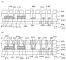
一方、特許文献1記載の技術には、MIMキャパシタの下層電極の下面にCu配線構造を接続させ、Cu配線を介して下層電極に電荷を供給する構成とした半導体装置が開示されている。同文献に記載された半導体装置を図7に示す。図7に示すように、銅配線34a〜dの上に、TiN膜38、SiO2膜39およびTiN膜40が、それぞれ100nm、40nm、150nm程度の膜厚で順次形成されており、TiN膜38がMIMの下部電極になっている。On the other hand, the technology described in Patent Document 1 discloses a semiconductor device having a structure in which a Cu wiring structure is connected to the lower surface of a lower electrode of an MIM capacitor and electric charges are supplied to the lower electrode via the Cu wiring. A semiconductor device described in this document is shown in FIG. As shown in FIG. 7, a TiN film 38, a SiO2 film 39, and a TiN film 40 are sequentially formed on the
ところが、上記公報記載のキャパシタは、以下のような課題を有していた。 However, the capacitor described in the above publication has the following problems.
第一に、銅配線上にバリアメタルを介してキャパシタ下層電極が積層した構造を有するため、依然、下層電極の平坦性が困難であった。第二に、バリアメタルは通常、高抵抗材料からなるため、下部電極の抵抗が高くなるという課題を有していた。膜厚を厚くすることで低抵抗化を図ることも考えられるが、TiNなどのバリアメタルは、一般に内部応力が高く、膜厚を厚くすることにも限界があった。第三に、バリアメタルが高抵抗、高内部応力であるため、大面積化することが困難であり、大きな容量を有するキャパシタを形成することが難しかった。 First, since the capacitor lower layer electrode is laminated on the copper wiring via the barrier metal, the flatness of the lower layer electrode is still difficult. Secondly, since the barrier metal is usually made of a high-resistance material, there is a problem that the resistance of the lower electrode is increased. Although it is conceivable to reduce the resistance by increasing the film thickness, barrier metals such as TiN generally have high internal stress, and there is a limit to increasing the film thickness. Third, since the barrier metal has high resistance and high internal stress, it is difficult to increase the area, and it is difficult to form a capacitor having a large capacity.
以上のように、配線の上部にMIMキャパシタを設ける構成においては、下部電極の平坦性が損なわれたり、下部電極の材料の選択に制限が加わる結果、所望の性能を有するキャパシタを得ることが困難となっていた。 As described above, in the configuration in which the MIM capacitor is provided on the upper part of the wiring, it is difficult to obtain a capacitor having desired performance as a result of the flatness of the lower electrode being impaired or the selection of the material of the lower electrode being restricted. It was.
本発明は、上記事情に鑑みなされたものであって、その目的とするところは、信頼性の高いMIM構造を有するキャパシタを設けた半導体装置を提供することにある。 The present invention has been made in view of the above circumstances, and an object thereof is to provide a semiconductor device provided with a capacitor having a highly reliable MIM structure.
本発明によれば、半導体基板と、半導体基板の上部に設けられた下部配線と、該下部配線を埋めこむ第1層間絶縁膜と、第1層間絶縁膜上に設けられた下部電極、その上部に設けられる上部電極、および、これらの電極に挟まれた誘電膜を有するMIMキャパシタと、MIMキャパシタを埋めこむ第2層間絶縁膜と、第2層間絶縁膜の上部に設けられた上部配線と、前記第1層間絶縁膜と前記第2層間絶縁膜との間に設けられた第3層間絶縁膜とを含み、下部電極が上部配線と電気的に接続され、前記第3層間絶縁膜は、SiO2、SiOC、SiOFからなるグループから選択された材料からなるか、またはSiO2、SiOC、SiOFからなるグループから選択された材料の組合せからなる、ことを特徴とする半導体装置が提供される。According to the present invention, a semiconductor substrate, a lower wiring provided above the semiconductor substrate, a first interlayer insulating film filling the lower wiring, a lower electrode provided on the first interlayer insulating film, and an upper portion thereof An MIM capacitor having a dielectric film sandwiched between these electrodes, a second interlayer insulating film embedded in the MIM capacitor, an upper wiring provided on the second interlayer insulating film,A third interlayer insulating film provided between the first interlayer insulating film and the second interlayer insulating film, wherein a lower electrode is electrically connected to an upper wiring, andthe third interlayer insulating film is made of SiO2. A semiconductor devicecomprising a material selected from the group consisting ofSiO2, SiOC, and SiOF, ora combination of materials selected from the group consisting ofSiO2, SiOC, and SiOF is provided. The
本発明は、下部配線と上部配線との間に挟まれた領域にMIMキャパシタを設けた半導体装置に関するものである。下部電極が第3層間絶縁膜上に形成されるため、下部電極の平坦性が良好となる。また、第1層間絶縁膜中に、下部配線と下部電極とを接続する部材を設けず、下部電極が上部配線と電気的に接続された構成としているため、下部電極の材料選択の自由度が向上する。この結果、下部電極の低抵抗化、大面積化を図ることができる。従来技術においては、下部電極は、下部配線と接する形で設けられており、下部銅配線やその上に設けられたバリアメタル上に下部電極を形成していたため、下部電極の材料選択に一定の制限があったが、本発明では下部電極を上部配線と接続する形態としているため、このような制限が解消される。The present invention relates to a semiconductor device in which an MIM capacitor is provided in a region sandwiched between a lower wiring and an upper wiring. Since the lower electrode is formed on thethird interlayer insulating film, the flatness of the lower electrode is improved. In addition, since a member for connecting the lower wiring and the lower electrode is not provided in the first interlayer insulating film, and the lower electrode is electrically connected to the upper wiring, the degree of freedom in selecting the material of the lower electrode is increased. improves. As a result, it is possible to reduce the resistance and area of the lower electrode. In the prior art, the lower electrode is provided in contact with the lower wiring, and the lower electrode is formed on the lower copper wiring and the barrier metal provided on the lower copper wiring. Although there is a limitation, in the present invention, since the lower electrode is connected to the upper wiring, such limitation is eliminated.
本発明において、上部配線とは、第2層間絶縁膜の上部にある配線群全体をさすこととする。 In the present invention, the upper wiring means the entire wiring group above the second interlayer insulating film.
また、上部電極と下部電極とが、異なる導電材料により構成されていてもよい。ここで、上部電極と下部電極では要求される特性が異なる場合がある。たとえば、下部電極は上部配線と接続するために面積を広くすることが好ましく、そのため低抵抗材料などを用いることが望ましい場合がある。また、上部電極は容量膜上に形成される関係で、当該容量膜上に良好に形成できる材料を用いることが望ましい場合がある。上部電極と下部電極とが異なる導電材料により構成されることにより、たとえば、MIMキャパシタの電極形成プロセス(電極形状に加工するエッチング等)に好適となるように、各電極の材料をそれぞれ独立に選択することができる。また、各電極と同一水準に、同一プロセスにて抵抗やインダクタ等の素子を形成する場合、これらの素子の設計に合わせて電極材料を選択することも可能となる。 Further, the upper electrode and the lower electrode may be made of different conductive materials. Here, the required characteristics may differ between the upper electrode and the lower electrode. For example, it is preferable to increase the area of the lower electrode in order to connect to the upper wiring, and therefore it may be desirable to use a low resistance material or the like. In addition, since the upper electrode is formed on the capacitor film, it may be desirable to use a material that can be satisfactorily formed on the capacitor film. By configuring the upper and lower electrodes with different conductive materials, each electrode material can be independently selected so that it is suitable for the MIM capacitor electrode formation process (such as etching to process the electrode shape). can do. Further, when elements such as resistors and inductors are formed at the same level as each electrode by the same process, it is possible to select an electrode material in accordance with the design of these elements.
本発明において、下部電極および上部電極は、同じ上部配線から接続されていてもよいし、異なる上部配線から接続されていてもよい。 In the present invention, the lower electrode and the upper electrode may be connected from the same upper wiring or may be connected from different upper wirings.
また、上層配線は銅配線であってもよく、下層配線は銅配線であってもよい。 Further, the upper layer wiring may be a copper wiring, and the lower layer wiring may be a copper wiring.
本発明において、銅配線とは、銅のみにより構成される配線だけでなく、銅を主成分として構成される配線のことをも含むこととする。 In the present invention, the copper wiring includes not only wiring composed only of copper but also wiring composed mainly of copper.
また、下部電極は、上部電極の外周縁よりも外方へ張り出した部分を有し、第1接続プラグは、上記部分と接続してもよい。こうすることにより、下部電極と上部配線とを第1接続プラグにより好適に接続することができる。 In addition, the lower electrode may have a portion protruding outward from the outer peripheral edge of the upper electrode, and the first connection plug may be connected to the above portion. By doing so, the lower electrode and the upper wiring can be suitably connected by the first connection plug.
また、下部電極と同一レベルに設けられ、下部電極と同一材料および同一膜厚からなる第1抵抗体を備えてもよいし、上部電極と同一レベルに設けられ、上部電極と同一材料および同一膜厚からなる第2抵抗体を備えてもよい。この構成によれば、MIMキャパシタと抵抗を含み、製造効率に優れた半導体装置が実現される。 Further, the first resistor may be provided at the same level as the lower electrode, and may be provided with the same material and the same film thickness as the lower electrode. You may provide the 2nd resistor which consists of thickness. According to this configuration, a semiconductor device including an MIM capacitor and a resistor and having excellent manufacturing efficiency is realized.
また、下部電極と同一レベルに設けられ、下部電極と同一材料および同一膜厚からなる複数の第1導電体と、上部配線と第1導電体とを接続する複数のビアとにより構成されるインダクタを備えてもよい。この構成によれば、MIMキャパシタとインダクタを含み、製造効率に優れた半導体装置が実現される。 Further, an inductor provided at the same level as the lower electrode and including a plurality of first conductors made of the same material and the same film thickness as the lower electrode, and a plurality of vias connecting the upper wiring and the first conductor. May be provided. According to this configuration, a semiconductor device including an MIM capacitor and an inductor and excellent in manufacturing efficiency is realized.
本発明によれば、半導体基板の上部に下部配線を形成する工程と、下部配線を埋めこむ第1層間絶縁膜と、前記第1層間絶縁膜上に第3層間絶縁膜を形成する工程と、第3層間絶縁膜上に、下部電極、誘電膜および上部電極が積層してなるMIMキャパシタを形成する工程と、MIMキャパシタを埋めこむ第2層間絶縁膜を形成する工程と、第2層間絶縁膜中に、下部電極に到達するビアホールを形成する工程と、ビアホールを導電膜で埋め込み、接続プラグを形成する工程と、第2層間絶縁膜の上部に、接続プラグと接続する上部配線を形成する工程とを含み、前記第3層間絶縁膜は、SiO2、SiOC、SiOFからなるグループから選択された材料からなるか、またはSiO2、SiOC、SiOFからなるグループから選択された材料の組合せからなることを特徴とする半導体装置の製造方法が提供される。
また、本発明によれば、半導体基板と、半導体基板の上部に設けられた下部配線と、該下部配線を埋めこむ第1層間絶縁膜と、第1層間絶縁膜上に設けられた下部電極、その上部に設けられる上部電極、および、これらの電極に挟まれた誘電膜を有するMIMキャパシタと、MIMキャパシタを埋めこむ第2層間絶縁膜と、第2層間絶縁膜の上部に設けられた上部配線と、前記第1層間絶縁膜と前記第2層間絶縁膜との間に設けられ、平坦化された第3層間絶縁膜とを含み、下部電極が上部配線と電気的に接続される、ことを特徴とする半導体装置が提供される。According to the present invention, a step of forming a lower wiring on the semiconductor substrate, a first interlayer insulating film filling the lower wiring, a step of forming athird interlayer insulating film on the first interlayer insulating film , Forming a MIM capacitor formed by laminating a lower electrode, a dielectric film and an upper electrode on thethird interlayer insulating film; forming a second interlayer insulating film filling the MIM capacitor; and a second interlayer insulating film A step of forming a via hole reaching the lower electrode, a step of filling the via hole with a conductive film to form a connection plug, and a step of forming an upper wiring connected to the connection plug on the second interlayer insulating filmlook including thedoor, the third interlayer insulatingfilm,SiO 2, SiOC, or comprises a material selected from the group consisting of SiOF, orSiO2, SiOC, selected from the group consisting of SiOF There is provided a method for manufacturing a semiconductor devicecomprising a combination of materials .
Further, according to the present invention, a semiconductor substrate, a lower wiring provided on the semiconductor substrate, a first interlayer insulating film filling the lower wiring, a lower electrode provided on the first interlayer insulating film, An upper electrode provided thereon, an MIM capacitor having a dielectric film sandwiched between these electrodes, a second interlayer insulating film embedded in the MIM capacitor, and an upper wiring provided above the second interlayer insulating film And a flattened third interlayer insulating film provided between the first interlayer insulating film and the second interlayer insulating film, wherein the lower electrode is electrically connected to the upper wiring. A semiconductor device is provided.
本発明によれば、信頼性の高いMIM構造を有するキャパシタを設けた半導体装置を提供することができる。 According to the present invention, a semiconductor device provided with a capacitor having a highly reliable MIM structure can be provided.
以下、本発明の実施の形態について図面を用いて説明する。なお、すべての図面において、同様な構成要素には、同様の符号を付し、適宜説明を省略する。 Hereinafter, embodiments of the present invention will be described with reference to the drawings. In all the drawings, similar constituent elements are denoted by the same reference numerals, and description thereof will be omitted as appropriate.
第一の実施形態
本実施形態に係る半導体装置は、多層銅配線を含むロジック回路素子中に、MIMキャパシタ、抵抗素子といった受動素子を設けた構造を具備する。First Embodiment A semiconductor device according to this embodiment includes a structure in which a passive element such as an MIM capacitor or a resistance element is provided in a logic circuit element including a multilayer copper wiring.
図1は、本実施形態に係る半導体装置200の構成を示す断面図である。 FIG. 1 is a cross-sectional view showing a configuration of a
半導体装置200は、シリコン基板(不図示)、第1銅配線層202、層間絶縁膜206、受動素子層250、第2銅配線層239が、この順に積層された構成を有する。第1銅配線層202および第2銅配線層239は、それぞれ、たとえば6層〜10層などの多層配線中の銅配線である。第1銅配線層202は、トランジスタが形成された層の直上にある第1層目の銅配線層に対応する。第2銅配線層239は、トランジスタが形成された層の直上にある第2層目の銅配線層に対応する。 The
第1銅配線層202は、絶縁膜204中に下部銅配線214が埋設された構成を有している。また、第2銅配線層239は、絶縁膜230中に上部銅配線238が埋設された構成を有している。 The first
本実施形態では、これらの銅配線層の間に、MIMキャパシタ、抵抗素子といった受動素子を設けられた受動素子層250が配置されている。受動素子層250の厚さは、0.8μm〜2μm程度である。 In this embodiment, a
ビアプラグ240は上部銅配線238と第2抵抗素子218との間を電気的に接続し、ビアプラグ241は上部銅配線238と第1抵抗素子224との間を電気的に接続し、ビアプラグ243は上部銅配線238と下部銅配線214との間を電気的に接続している。また、コンタクト217は上部銅配線238と上部電極216との間を電気的に接続し、コンタクト219は上部銅配線238と下部電極220との間を電気的に接続している。 The via
受動素子層250は、上記構成の第1銅配線層202および第2銅配線層239に挟まれた位置に設けられている。受動素子層250には、MIM構造を有するキャパシタ260、第2抵抗素子218および第1抵抗素子224といった受動素子が形成されており、さらに、ダミー金属膜226a、ダミー金属膜226bが形成されている。 The
キャパシタ260は、上部電極216、下部電極220、および、これら2つの電極に挟まれ容量膜として機能する誘電体膜210から構成されている。下部電極220は、上部電極216の外周縁よりも外方へ張り出した部分を有し、この張り出した部分と上部銅配線238とがコンタクト219を介して接合している。また、上部電極216は、上部銅配線238とコンタクト217を介して接合している。 The
下部電極220はTi、TiN、Al、Ti、TiNが下からこの順で積層した金属膜からなっている。このようなAlを含む多層金属膜により下部電極を構成することで、下部電極の低抵抗化を図ることができる。また、電極抵抗が低減される結果、電極面積を増大させ容量の向上を図ることが可能となる。ここで、Al層の厚さは、100nm程度以上であればよく、100nm〜200nmの範囲が好ましい。下部電極220全体の厚さとしては、たとえば、400nm程度とするのがよい。 The
上部電極216は、たとえば、高融点金属からなるバリアメタルにより構成されている。こうすることにより、上部電極216は数十Ωから数キロΩの抵抗値を有し、MIMキャパシタを構成する上部電極の抵抗体としての機能を発揮することができる。なお、本実施形態においては、上部電極216を構成する材料としてTaNを用いているが、たとえば、TiN、Ta、Wなどを用いてもよい。 The
誘電体膜210は、キャパシタの容量膜として機能する。誘電体膜210を構成する材料としては、SiO2、SiON、SiOC、SiN、Ta2O5等のほか、ZrOx、HfOx、ZrSiOx、HfSiOx、Al2O3等のいわゆるHigh−K材料や、PZT、PLZT等のペロブスカイト構造を有する材料等を用いることができる。誘電体膜210の膜厚は、材料に応じて適宜選択されるが、たとえば、20nm〜100nm程度とする。本実施形態では、材料としてSiO2を用い、膜厚を50nmとしている。The
ここで、下部電極220、誘電体膜210および上部電極216の合計厚みは、0.5μm以下とすることが好ましい。こうすることにより、ビアホール236の歩留まりを向上させることができる。また、下部電極220と上部電極216の厚みは、電気抵抗値上昇による影響を考慮し、厚めに設定されるのが好ましい。そのため、誘電体膜210の厚みを薄く設定することが好ましく、その結果、MIMキャパシタの容量の設計可能範囲を広くとることができる。また、合計厚みは、0.3μm以下とすることがより好ましい。こうすることにより、受動素子層250全体の平坦性が良好となり、その上に積層される多層配線を歩留まり良く形成することができる。 Here, the total thickness of the
第1抵抗素子224は、キャパシタ260の下部電極220と同一工程で形成される。この結果、第1抵抗素子224と下部電極220とは、同一レベルに設けられ、同一材料および同一膜厚となっている。第1抵抗素子224は、ビアプラグ241により上部銅配線238と接続されている。 The
第2抵抗素子218は、キャパシタ260の上部電極216と同一工程で形成される。この結果、第2抵抗素子218と上部電極216とは、同一レベルに設けられ、同一材料および同一膜厚となっている。第2抵抗素子218は、キャパシタ260と同じ積層構造を有する構造体の上部電極を利用した形態となっており、この上部電極をビアプラグ240により上部銅配線238と接続し抵抗体として利用したものである。なお、第2抵抗素子218の下部に配置されている下部電極222は、配線に接続されておらず浮遊電位となっており、素子として機能していない。 The
以上のように、第1抵抗素子224は、下部電極220と同じAlを含む金属膜により構成され、第2抵抗素子218は、上部電極216と同じTaNにより構成されている。本実施形態によれば、このように材料の異なる2種類の抵抗素子を、キャパシタ260形成と同一プロセスで形成することができる。 As described above, the
ダミー金属膜226aおよびダミー金属膜226bは、下部電極220、下部電極222および第1抵抗素子224と同一材料、同一膜厚で形成されている。ダミー金属膜226aおよびダミー金属膜226bは、配線に接続されておらず浮遊電位となっており、素子として機能していない。 The
次に、図1に示した半導体装置200の製造工程について説明する。 Next, a manufacturing process of the
図2〜図4は、本実施形態に係る半導体装置200の製造工程を示す断面図である。 2 to 4 are cross-sectional views showing the manufacturing process of the
はじめに、図2(a)に示すように、第1銅配線層202および層間絶縁膜206を積層し、その上にAl含有多層膜208、誘電体膜210および上部導電膜212をこの順で積層した構造を得る。はじめに、ダマシンプロセスを用いて絶縁膜204中に下部銅配線214が埋設された配線層を得る。次いでその上に、CVD法などにより層間絶縁膜206を成膜する。その後、スパッタリング法を用い、Ti、TiN、Al、Ti、TiNをこの順で成膜することにより、5層構造のAl含有多層膜208を成膜する。このAl含有多層膜208の上に、CVD法などを用いて誘電体膜210を成膜し、その上に、スパッタリング法などを用いて上部導電膜212を成膜する(図2(a))。ここで、層間絶縁膜206および誘電体膜210を構成する材料としては、SiO2、SiON、SiOC、SiN、Ta2O5等のほか、ZrOx、HfOx、ZrSiOx、HfSiOx、Al2O3等のいわゆるHigh−K材料や、PZT、PLZT等のペロブスカイト構造を有する材料などを用いることができる。ここで、層間絶縁膜206および誘電体膜210の膜厚は、材料に応じて適宜選択されるが、本実施形態では、層間絶縁膜206の材料としてSiOFを用い、誘電体膜210の材料としてSiO2を用いている。また、膜厚をそれぞれ、0.1μm、50nmとしている。第1銅配線層202は、下部銅配線214および絶縁膜204を内部に有する。First, as shown in FIG. 2A, a first
Al含有多層膜208は、図中下から、Ti、TiN、Al、Ti、TiNがこの順に積層された構造を有し、Alの層を主として構成されている。ここで、Alの層の厚さとしては、100nm程度以上であればよく、100nm〜200nmの範囲内が好ましく用いられる。また、Al含有多層膜208の厚さとしては、たとえば、400nm程度が用いられる。 The Al-containing
上部導電膜212は、たとえば、高融点金属からなるバリアメタルにより構成されている。本実施形態においてはTaNを用いているが、たとえば、TiN、Ta、Wなどを用いてもよい。 The upper
ここで、上部導電膜212と、誘電体膜210と、Al含有多層膜208とを合わせた厚さは、0.5μm以下が好ましい。こうすることにより、キャパシタ260の容量の設計可能範囲を広くとることができる。また、0.3μm以下とすることがより好ましい。こうすることにより、受動素子層250全体の平坦性が良好となり、その上に積層される多層配線を歩留まり良く形成することができる。 Here, the total thickness of the upper
後述する上部電極216などを形成する領域を画定するために、上部導電膜212上にレジスト膜を形成し、フォトリソグラフィーにより、レジストパターンを形成する。次にレジストパターンをマスクとして、選択的にドライエッチングすることによりキャパシタ260を構成する上部電極216、抵抗体として用いる第2抵抗素子218を形成する(図2(b))。 A resist film is formed on the upper
後述する下部電極220などを形成する領域を画定するために、誘電体膜210と上部電極216と第2抵抗素子218との上に、レジスト膜を形成し、フォトリソグラフィーにより、レジストパターンを形成する。次にレジストパターンをマスクとして、選択的にドライエッチングすることにより、誘電体膜210の一部を除去すると同時に、キャパシタ260を構成する下部電極220、浮遊電極とする下部電極222、抵抗体として用いる第1抵抗素子224、配線としては用いずダミーとするダミー金属膜226a、ダミー金属膜226bを形成する(図2(c))。 A resist film is formed on the
CVD法などを用いて、層間絶縁膜228を成膜後、たとえば、CMP技術などを用いて、層間絶縁膜228を平坦化する(図3(a))。層間絶縁膜228を構成する材料としては、SiO2、SiON、SiOC、SiN、Ta2O5等のほか、ZrOx、HfOx、ZrSiOx、HfSiOx、Al2O3等のいわゆるHigh−K材料や、PZT、PLZT等のペロブスカイト構造を有する材料などが用いられる。ここで、層間絶縁膜206と層間絶縁膜228とを合わせた厚さは、0.8μm〜2μm程度である。After forming the
層間絶縁膜228上に、たとえば、CVD法などを用いて、絶縁膜230を成膜する(図3(b))。絶縁膜230を構成する材料としては、SiO2、SiON、SiOC、SiN、Ta2O5等のほか、ZrOx、HfOx、ZrSiOx、HfSiOx、Al2O3等のいわゆるHigh−K材料や、PZT、PLZT等のペロブスカイト構造を有する材料などが用いられる。An insulating
絶縁膜230内に銅配線用溝232を形成する領域を画定するために、絶縁膜230上にレジスト膜を形成し、フォトリソグラフィーにより、レジストパターンを形成する。次にレジストパターンをマスクとして、ドライエッチングすることにより、絶縁膜230の一部が除去されて、銅配線用溝232が形成される(図3(c))。 In order to define a region for forming the
銅配線用溝232を埋め込むように、絶縁膜230上にレジスト膜を成膜する。次に、フォトリソグラフィーにより、レジスト膜上にレジストパターンを形成する。ついで、レジストパターンをマスクとして、ドライエッチングすることにより、層間絶縁膜228の一部、層間絶縁膜206の一部を除去する。この手順により、ビアホール236を形成する。(図4(a))。 A resist film is formed on the insulating
ビアホール236および銅配線用溝232内に、それぞれスパッタリング法などにより、たとえば、W、WN、Ta、TaN、Ti、TiNなどからなるバリアメタルを成膜する(不図示)。次に、バリアメタル上に、ビアホール236および銅配線用溝232を埋め込むように、たとえば、電界めっき法などにより銅膜を成膜する。ついで、CMP技術などを用いて銅膜の表面を平坦化し、その後、不要なバリアメタルおよび銅膜を除去することにより、コンタクト217、コンタクト219、ビアプラグ240、ビアプラグ241、ビアプラグ243と、上記コンタクトおよびビアプラグが連結された上部銅配線238とを同時に形成する。(図4(b))。 A barrier metal made of, for example, W, WN, Ta, TaN, Ti, TiN or the like is formed in the via
本実施形態における半導体装置200の効果について以下に説明する。 The effects of the
本実施形態において、MIM構造を有するキャパシタ260は、多層配線層を構成する第1銅配線層202と第2銅配線層239との間の層に設けられている。このため、製造効率に優れ、素子レイアウト効率に優れる半導体装置を実現できる。ロジック回路素子等における多層配線パターンの設計にあっては、以前に作成した回路パターンを用いつつ必要な箇所を修正する手法がしばしば採用される。本実施形態によれば、こうした手法を好適に実現することができる。すなわち、受動素子の回路パターンを変更しようとしたとき、受動素子層250のみを設計変更すればよく、かかる設計変更は、他の配線層に影響を与えることがない。したがって、特許文献1記載の技術に代表される従来技術のように、多層配線層の最上層に配線と混在させた形態でMIMキャパシタを設ける構成と比較し、素子設計のリードタイムを大幅に短縮し得る製造効率に優れる構造の半導体装置を実現できる。また、銅配線層中のスペースに受動素子を設ける構成に比べ、受動素子のレイアウトの自由度が向上する。 In the present embodiment, the
また、本実施形態では、キャパシタ260の下部電極220が、コンタクト219を介して上部銅配線238と接続した構造を採用する。そして、上部電極216の面積よりも下部電極220の面積を広くし、下部電極220の外縁部が上部電極216の外縁部よりも外側に張り出す形態とし、この張り出し部分にコンタクト219の底部が接続する構造を採用している。このため、素子設計のリードタイムを大幅に短縮できるとともに、製造効率に優れる半導体装置が実現される。 In the present embodiment, a structure in which the
受動回路の用途によっては、多層配線の下層に配置することが望まれる場合がある。ところが、下層に位置する配線層は一般に配線密度が高く、余剰スペースに受動素子を配置することは困難である。そこで本実施形態では、下部銅配線と上部銅配線との間に受動素子層250を介在させた構成としている。こうした受動素子層を介在させるにあたっては、周辺の銅配線との電気的接続を如何に確保するかが重要な技術的課題となるが、本実施形態では、キャパシタ260の上部電極216および下部電極220を、それぞれ、コンタクトを介して上部銅配線238と接続する構造としている。このため、受動素子層250を設けることによる膜厚の増大が最小限に抑制される。また、キャパシタ260の各電極に電圧を印加するための配線を上部配線の側にだけ設ければ済み、受動素子層250を設けることによる配線パターンの設計変更を最小限にすることができる。また、上部銅配線238と接続するコンタクトを、他の素子に配設されたビアプラグ(ビアプラグ240、241)や、上部銅配線238と下部銅配線214とを接続するビアプラグ243と同一工程で形成でき、製造効率にも優れる。 Depending on the application of the passive circuit, it may be desired to dispose it below the multilayer wiring. However, the wiring layer located in the lower layer generally has a high wiring density, and it is difficult to dispose passive elements in the surplus space. Therefore, in the present embodiment, the
ここで、上記のように下部電極220を大きくすると、下部電極220の電気抵抗値が高くなり、所望の電荷蓄積量を得ることが困難になる上、複数のキャパシタ間で容量のばらつきが生じることとなる。この結果、MIM構造を有するキャパシタ260を電池として用いる際の電源安定性や、LC回路を構成する素子として用いる際の高速動作性を得ることが難しくなる。こうしたことを解決するために、下部電極220を厚くして下部電極220の電気抵抗値を低くすることも考えられるが、従来のようにTiN、Tiなどのバリアメタルで下部電極を形成した構造では、下部電極の厚さを増すと内部応力が大きくなってしまい、周囲に設けられる絶縁膜との密着性が低下するという問題が生じる。これに対して本実施形態における下部電極220は、主にAlにより構成されているため、バリアメタルよりも電気抵抗値が低く、応力値も低い。したがって、電荷蓄積量および下部電極と絶縁膜との密着性への影響を抑制しつつ、コンタクト219による連結のために下部電極220の面積を広くとることが可能となる上、電気抵抗値を低くするために下部電極220の厚さを増すことができる。この結果、本実施形態によれば、従来にない大容量のMIMキャパシタを歩留まり良く製造することができる。 Here, when the
また、本実施形態において、Al含有多層膜208は、平坦化された層間絶縁膜206上に成膜されているので、Al含有多層膜208、誘電体膜210および上部導電膜212を平坦に成膜することができる。このため、MIM構造を有するキャパシタ260を構成する上部電極216と、下部電極220と、その間に挟まれる誘電体膜210の平坦性を向上させることができ、所望の容量のキャパシタ260を得ることができる。この結果、キャパシタ260を電池として用いる際の電源安定性や、キャパシタ260をLC回路を構成する素子として用いる際の高速動作性を得ることができるため、信頼性の高いMIM構造を有するキャパシタを備える半導体装置200が実現される。 In this embodiment, since the Al-containing
さらに、本実施形態において、Al含有多層膜208をドライエッチングして、下部電極220などを形成する際に、銅配線間を接続するビアプラグ243の近傍に、配線には用いないダミーのダミー金属膜226aおよびダミー金属膜226bが形成されている。このため、層間絶縁膜228を形成する際には、第1抵抗素子224だけでなく、ダミー金属膜226aおよびダミー金属膜226bの上にも形成されることとなる。それゆえ、ダミー金属膜を形成せずに、キャパシタや抵抗素子上に層間絶縁膜が形成される場合と比較して、キャパシタ260や第2抵抗素子218上に形成される層間絶縁膜の高さと、ダミー金属膜上に形成される層間絶縁膜の高さの差を小さくすることができる。そのため、CMP技術などにより層間絶縁膜228を平坦化することができ、層間絶縁膜228の上層に設けられる絶縁膜230および上部銅配線238を平坦化することが可能になる。したがって、銅配線用溝232やビアホール236を寸法精度良く形成することができる。この結果、上部銅配線238と各電極および抵抗素子とを正確に接続することができるため、信頼性の高いMIM構造を有するキャパシタを設けた半導体装置200が実現される。 Furthermore, in this embodiment, when the Al-containing
また、本実施形態において、キャパシタ260を構成する、上部電極216の膜厚と、誘電体膜210と、下部電極220との膜厚の合計値を、0.5μm以下としている。ここで、下部電極220と上部電極216の厚みは、電気抵抗値上昇によるMIMキャパシタ容量の設計可能範囲への影響を考慮し、厚めに設定されるのが好ましい。そのため、容量膜である誘電体膜210の厚みを薄く設定することが好ましい。ここで、容量膜の厚みの薄いキャパシタは容量値の設計範囲を広く設定することができる。このため、キャパシタ260について、所望のキャパシタ容量を得ることができる。また、ビアホール236を形成する際の歩留まりを向上させることができる。したがって、MIM構造を有するキャパシタ260を有する半導体装置200の製造プロセスにおける製造安定性を向上させつつ、キャパシタ260を電池として用いる際の電源安定性や、キャパシタ260をLC回路を構成する素子として用いる際の高速動作性を得ることができる。 In the present embodiment, the total value of the film thickness of the
また、本実施形態において、上部電極は主にTaNにより構成され、下部電極は主にAlにより構成されている。ここで、回路には色々な抵抗値を有する抵抗体を配置することが必要である。本実施形態においては、上部電極を構成する材料と、下部電極を構成する材料とを異なる材料とすることにより、抵抗体を構成する材料の面積や厚さを変えることなく、上部電極の抵抗値と下部電極の抵抗値とを異なるものとしている。この結果、集積度向上を図りつつ、抵抗値の異なる抵抗体を回路に配置することにより、信頼性の高いMIM構造を有するキャパシタを設けた半導体装置200が実現される。 In the present embodiment, the upper electrode is mainly made of TaN, and the lower electrode is mainly made of Al. Here, it is necessary to arrange resistors having various resistance values in the circuit. In the present embodiment, the material constituting the upper electrode and the material constituting the lower electrode are different from each other, thereby changing the resistance value of the upper electrode without changing the area and thickness of the material constituting the resistor. And the resistance value of the lower electrode are different. As a result, the
また、本実施形態において、抵抗体として用いられる第2抵抗素子218と第1抵抗素子224は、第2銅配線層239と第1銅配線層202との間にある層間絶縁膜228中に形成されている。しかし、特許文献1に代表される従来の技術においては、抵抗体は、MIM構造を有するキャパシタと同じ層ではなく、基板に近い層に設けられていた。このため、基板と抵抗体との間に発生する寄生容量の影響を受けてしまい、所望の抵抗値を得ることができなかった。この傾向は、高周波領域において特に顕著である。一方、本実施形態においては、抵抗体が層間絶縁膜228中に形成されているので、基板との間に発生する寄生容量の影響を抑制することができる。したがって、第1抵抗素子224と第2抵抗素子218は所望の抵抗値を得ることができる。 In the present embodiment, the
また、本実施形態においては、第2抵抗素子218や第1抵抗素子224のように、抵抗値の異なる抵抗体を、MIM構造を有するキャパシタの上部電極216および下部電極220を形成する際に、それぞれ同一平面上に、同時に形成している。したがって、MIM構造を有するキャパシタ260を搭載する半導体装置200に抵抗値の異なる抵抗体を形成するプロセスを簡略化することができる。 In the present embodiment, when the
また、本実施形態において、誘電体膜210上に形成された上部導電膜212をドライエッチングすることによって、上部電極216と第2抵抗素子218とが同時に形成されている。また、層間絶縁膜206上に形成されたAl含有多層膜208をドライエッチングすることによって、下部電極220、下部電極222、第1抵抗素子224、ダミー金属膜226aおよびダミー金属膜226bが同時に形成されている。したがって、MIM構造を有するキャパシタ260を搭載する半導体装置200を製造するプロセスを簡略化することができる。 In the present embodiment, the
第二の実施形態
本実施形態に係る半導体装置は、MIMキャパシタを有する層と同層にインダクタが設けられている。Second Embodiment In a semiconductor device according to this embodiment, an inductor is provided in the same layer as a layer having an MIM capacitor.
図5は、本実施形態に係る半導体装置300の構成を示す断面図であり、図6は、図5のインダクタ270を上面から見た構造を示す図である。図5において、インダクタ270は、下部電極220と同一レベルに設けられた第1導体242、第2導体244と、第3導体246、第4導体248、ビアプラグ245、上部銅配線238とにより構成されている。ここで、第1導体242の端部とビアプラグ245、第2導体244の端部とビアプラグ245、第3導体246の端部とビアプラグ245、第4導体248の端部とビアプラグ245とがそれぞれ接続されている。図6において、上部銅配線238、ビアプラグ245、第1導体242、ビアプラグ245、上部銅配線238、ビアプラグ245、第2導体244、ビアプラグ245、上部銅配線238、ビアプラグ245、第3導体246、ビアプラグ245、上部銅配線238、ビアプラグ245、第4導体248、ビアプラグ245、上部銅配線238が、この順に連結され、インダクタ270を形成している。すなわち、インダクタ270は、基板面と略水平な方向の軸の周りに導体が巻回した構造を有している。したがって、インダクタ270に通電すると、基板面と略水平な方向に磁界が発生する。 FIG. 5 is a cross-sectional view showing a configuration of the
次に、図5を用いて、半導体装置300の製造工程について説明する。半導体装置300の製造工程は、インダクタ270を構成する、第1導体242、第2導体244、第3導体246および第4導体248を形成する点、およびビアプラグ245を上記インダクタ270を構成する電極に接続する点で、第一の実施形態と異なる。 Next, the manufacturing process of the
第一の実施形態で説明した図2(a)の工程の後、上部導電膜212上にレジスト膜を形成し、フォトリソグラフィーにより、レジストパターンを形成する。次にレジストパターンをマスクとして、上部導電膜212を選択的にドライエッチングすることにより上部電極216、第1抵抗素子218を形成する。 After the step of FIG. 2A described in the first embodiment, a resist film is formed on the upper
次に、下部電極を形成する領域を画定するために、誘電体膜210と上部電極216と第2抵抗素子218との上に、レジスト膜を形成し、フォトリソグラフィーにより、レジストパターンを形成する。次にレジストパターンをマスクとして、ドライエッチングすることにより、誘電体膜210の一部を除去すると同時に、キャパシタ260を構成する下部電極220、浮遊電極とする下部電極222、抵抗体として用いる第1抵抗素子224、配線としては用いずダミーとするダミー金属膜226a、ダミー金属膜226b、インダクタを構成する第1導体242、第2導体244、第3導体246および第4導体248を形成する。 Next, in order to define a region for forming the lower electrode, a resist film is formed on the
ついで、CVD法などを用いて、層間絶縁膜228を成膜後、たとえば、CMP技術などを用いて、層間絶縁膜228を平坦化する。層間絶縁膜228を構成する材料としては、SiO2、SiON、SiOC、SiN、Ta2O5等のほか、ZrOx、HfOx、ZrSiOx、HfSiOx、Al2O3等のいわゆるHigh−K材料や、PZT、PLZT等のペロブスカイト構造を有する材料などが用いられる。ここで、層間絶縁膜206と層間絶縁膜228とを合わせた厚さは、0.8μm〜2μm程度である。Next, after the
次に、層間絶縁膜228上に、CVD法などを用いて、絶縁膜230を成膜する。絶縁膜230を構成する材料としては、SiO2、SiON、SiOC、SiN、Ta2O5等のほか、ZrOx、HfOx、ZrSiOx、HfSiOx、Al2O3等のいわゆるHigh−K材料や、PZT、PLZT等のペロブスカイト構造を有する材料などが用いられる。Next, the insulating
ついで、絶縁膜230内に銅配線用溝232を形成する領域を画定するために、絶縁膜230上にレジスト膜を形成し、フォトリソグラフィーにより、レジストパターンを形成する。次にレジストパターンをマスクとして、ドライエッチングすることにより、絶縁膜230の一部が除去されて、銅配線用溝232が形成される。 Next, a resist film is formed on the insulating
銅配線用溝232を埋め込むように、絶縁膜230上にレジスト膜を成膜する。次に、フォトリソグラフィーにより、レジスト膜上にレジストパターンを形成する。ついで、レジストパターンをマスクとして、ドライエッチングすることにより、層間絶縁膜228の一部、層間絶縁膜206の一部を除去する。この手順により、ビアホール236を形成する。 A resist film is formed on the insulating
ビアホール236および銅配線用溝232内に、それぞれスパッタリング法により、たとえば、W、WN、Ta、TaN、Ti、TiNなどからなるバリアメタルを成膜する。次に、バリアメタル上に、ビアホール236および銅配線用溝232を埋め込むように、たとえば、電界めっき法により銅膜を成膜する。ついで、たとえば、CMP技術を用いて銅膜の表面を平坦化し、その後、不要なバリアメタルおよび銅膜を除去することにより、コンタクト217、コンタクト219、ビアプラグ240、ビアプラグ241、ビアプラグ243、ビアプラグ245と、上記コンタクトとビアプラグが連結された上部銅配線238とを同時に形成する。 A barrier metal made of, for example, W, WN, Ta, TaN, Ti, TiN or the like is formed in each of the via
本実施形態において、半導体装置300に、インダクタ270を設けた構造としたことの効果について以下に説明する。 In the present embodiment, the effect of providing the
本実施形態において、インダクタ270は、第2銅配線層239と第1銅配線層202との間の層に基板とほぼ水平に設けられている。そのため、多層銅配線層間のスペースを有効に活用して、インダクタ270をレイアウトするとともに、MIM構造を有するキャパシタ260を設けることが可能になる。このため、コイル形成のためのスペースを別途準備する必要がなく、コイルを簡易に形成することができるとともに、デッドスペースを利用してコイルを形成することができるので、省スペース化ができる。また、コイルの磁束が基材に水平な方向に生じるので、半導体装置300に含まれる他の部材との干渉を低減することができる。これにより、コイルの設置場所を考慮することなく他の部材の設計を行うことができ、レイアウトの自由度を高めることができる。したがって、信頼性の高いMIM構造を有するキャパシタ260およびインダクタ270などを用いたLCR回路を備えた半導体装置300が実現できる。 In the present embodiment, the
また、本実施形態において、インダクタ270を構成する、第1導体242、第2導体244、第3導体246および第4導体248は、Al含有多層膜208をドライエッチングすることによって、キャパシタ260を構成する下部電極220などと同時に同一平面状に形成されている。したがって、MIM構造を有するキャパシタ260およびインダクタ270などを用いたLCR回路を備えた半導体装置300を製造するプロセスを簡略化することができる。 In this embodiment, the
以上、本発明を実施の形態に基づいて説明した。この実施の形態はあくまで例示であり、種々の変形例が可能なこと、またそうした変形例も本発明の範囲にあることは当業者に理解されるところである。 The present invention has been described based on the embodiments. This embodiment is merely an example, and it will be understood by those skilled in the art that various modifications are possible and that such modifications are also within the scope of the present invention.
たとえば、上記実施形態においては、ダミーのダミー金属膜226aおよびダミー金属膜226bを設けて層間絶縁膜228を平坦化する形態について説明したが、ダミーのダミー金属膜226aおよびダミー金属膜226bを設けずに、上部電極の膜厚と下部電極の膜厚の合計値を0.3μm以下とすることで、層間絶縁膜228を平坦化してもよい。上部電極の膜厚と下部電極の膜厚の合計値を0.3μm以下とすることにより、下部電極220などを形成した後に成膜される層間絶縁膜228の高低差が小さくなり、CMP技術などにより層間絶縁膜228を平坦化することができる。そのため、層間絶縁膜228の上層に設けられる絶縁膜230および上部銅配線238を平坦化することが可能になる。したがって、ビアホール236を所望の位置に形成することができる。この結果、上部銅配線238と下部電極220とを正確に接続することができるため、信頼性の高いMIM構造を有するキャパシタを設けた半導体装置200を製造することができる。 For example, in the above embodiment, the dummy
また、上記実施形態においては、下部銅配線214と上部銅配線238を用いる形態について説明したが、たとえば、CuAl、CuSiなどのように、銅を主成分とする配線などであってもよい。 In the above embodiment, the form using the
また、上記実施形態においては、Al含有多層膜208が、図中下から、Ti、TiN、Al、Ti、TiNの順に積層された形態について説明したが、Al単独であってもよい。 Moreover, in the said embodiment, although the Al-containing
また、上記実施形態においては、Al含有多層膜208を構成する主な材料として、Alを用いた形態について説明したが、Al−Si、Al−Si−Cuなどを主な材料として用いてもよい。 Moreover, in the said embodiment, although the form using Al was demonstrated as a main material which comprises the Al containing
また、上記実施形態においては、上部導電膜212を構成する材料としてTaNを用いた形態について説明したが、W、WN、Ta、Ti、TiNなどを用いてもよい。 In the above-described embodiment, the form using TaN as the material constituting the upper
また、上記実施形態においては、Al含有多層膜208を構成する主な材料としてAl、上部導電膜212を構成する材料としてTaNを用いた形態について説明したが、上部導電膜212を構成する材料の抵抗値よりも層間絶縁膜206の上に形成される膜を構成する材料の抵抗値が低ければよい。 Further, in the above-described embodiment, the form in which Al is used as the main material constituting the Al-containing
また、上記実施形態においては、デュアルダマシンプロセスを用いた形態について説明したが、シングルダマシンプロセスを用いてもよい。 Further, in the above embodiment, the form using the dual damascene process has been described, but a single damascene process may be used.
また、上記実施形態においては、ビアプラグを構成する材料として銅を用いる形態について説明したが、シングルダマシンプロセスを用いた場合には、ビアプラグとして、たとえば、タングステンなどを用いてもよい。 Further, in the above-described embodiment, the form in which copper is used as the material constituting the via plug has been described. However, when a single damascene process is used, for example, tungsten or the like may be used as the via plug.
また、上記実施形態においては、第1導体242、第2導体244、第3導体246、第4導体248の4個の導体を用いてインダクタ270を形成する形態について説明したが、たとえば、6個や8個などの導体を用いてインダクタを形成してもよい。 In the above embodiment, the
200 半導体装置
202 第1銅配線層
204 絶縁膜
206 層間絶縁膜
208 Al含有多層膜
210 誘電体膜
212 上部導電膜
214 下部銅配線
216 上部電極
217 コンタクト
218 第2抵抗素子
219 コンタクト
220 下部電極
222 下部電極
224 第1抵抗素子
226a ダミー金属膜
226b ダミー金属膜
228 層間絶縁膜
230 絶縁膜
232 銅配線用溝
236 ビアホール
238 上部銅配線
239 第2銅配線層
240 ビアプラグ
241 ビアプラグ
242 第1導体
243 ビアプラグ
244 第2導体
245 ビアプラグ
246 第3導体
248 第4導体
250 受動素子層
260 キャパシタ
270 インダクタ200
Claims (18)
Translated fromJapanese前記半導体基板の上部に設けられた下部配線と、
該下部配線を埋めこむ第1層間絶縁膜と、
前記第1層間絶縁膜上に設けられた下部電極、その上部に設けられる上部電極、および、これらの電極に挟まれた誘電膜を有するMIMキャパシタと、
前記MIMキャパシタを埋めこむ第2層間絶縁膜と、
前記第2層間絶縁膜の上部に設けられた上部配線と、
前記第1層間絶縁膜と前記第2層間絶縁膜との間に設けられた第3層間絶縁膜と、
を含み、
前記下部電極が前記上部配線と電気的に接続され、
前記第3層間絶縁膜は、SiO2、SiOC、SiOFからなるグループから選択された材料からなるか、またはSiO2、SiOC、SiOFからなるグループから選択された材料の組合せからなる、ことを特徴とする半導体装置。A semiconductor substrate;
A lower wiring provided on an upper portion of the semiconductor substrate;
A first interlayer insulating film embedded in the lower wiring;
A MIM capacitor having a lower electrode provided on the first interlayer insulating film, an upper electrode provided thereon, and a dielectric film sandwiched between these electrodes;
A second interlayer insulating film for embedding the MIM capacitor;
An upper wiring provided on the second interlayer insulating film;
A third interlayer insulating film provided between the first interlayer insulating film and the second interlayer insulating film;
Including
The lower electrode is electrically connected to the upper wiring;
The third interlayer insulatingfilm, SiO2, SiOC, or comprises a material selected from the group consisting of SiOF, or consists ofSiO 2, SiOC, a combination of material selected from the group consisting of SiOF, and characterized in that Semiconductor device.
前記上部電極と前記下部電極とが、異なる導電材料により構成されていることを特徴とする半導体装置。The semiconductor device according to claim 1,
The semiconductor device, wherein the upper electrode and the lower electrode are made of different conductive materials.
前記下部配線が銅配線であることを特徴とする半導体装置。The semiconductor device according to claim 1 or 2,
The semiconductor device according to claim 1, wherein the lower wiring is a copper wiring.
前記上部配線が銅配線であることを特徴とする半導体装置。The semiconductor device according to claim 1,
A semiconductor device, wherein the upper wiring is a copper wiring.
前記第2層間絶縁膜中に設けられ、前記下部電極と前記上部配線とを電気的に接続する第1接続プラグと、
前記第2層間絶縁膜中に設けられ、前記上部電極と前記上部配線とを電気的に接続する第2接続プラグと、
を含むことを特徴とする半導体装置。The semiconductor device according to claim 1,
A first connection plug provided in the second interlayer insulating film and electrically connecting the lower electrode and the upper wiring;
A second connection plug provided in the second interlayer insulating film and electrically connecting the upper electrode and the upper wiring;
A semiconductor device comprising:
前記下部電極は、前記上部電極の外周縁よりも外方へ張り出した部分を有し、
前記第1接続プラグは、前記部分と接続することを特徴とする半導体装置。The semiconductor device accordingto claim5 ,
The lower electrode has a portion protruding outward from the outer peripheral edge of the upper electrode,
The semiconductor device, wherein the first connection plug is connected to the portion.
前記上部電極が、前記上部配線と電気的に接続されていることを特徴とする半導体装置。The semiconductor device according to claim 1,
The semiconductor device, wherein the upper electrode is electrically connected to the upper wiring.
前記下部電極はアルミニウム含有膜を含むことを特徴とする半導体装置。The semiconductor device according to claim 1,
The semiconductor device according to claim 1, wherein the lower electrode includes an aluminum-containing film.
前記下部電極の厚みが、300〜500nmであることを特徴とする半導体装置。The semiconductor device according to claim 1,
The thickness of the said lower electrode is 300-500 nm, The semiconductor device characterized by the above-mentioned.
前記下部電極と同一レベルに設けられ、前記下部電極と同一材料および同一膜厚からなる第1抵抗体を備えることを特徴とする半導体装置。The semiconductor device according to claim 1,
A semiconductor device comprising a first resistor provided at the same level as the lower electrode and made of the same material and the same film thickness as the lower electrode.
前記上部電極と同一レベルに設けられ、前記上部電極と同一材料および同一膜厚からなる第2抵抗体を備えることを特徴とする半導体装置。The semiconductor device according to claim 1,
A semiconductor device comprising: a second resistor provided at the same level as the upper electrode and made of the same material and the same film thickness as the upper electrode.
前記下部電極と同一レベルに設けられ、前記下部電極と同一材料および同一膜厚からなる第1抵抗体と、
前記上部電極と同一レベルに設けられ、前記上部電極と同一材料および同一膜厚からなる第2抵抗体と、を備え、
前記第1抵抗体と前記第2抵抗体とが、異なる材料からなることを特徴とする半導体装置。10. The semiconductor device according to claim 1, further comprising:
A first resistor which is provided at the same level as the lower electrode and is made of the same material and the same film thickness as the lower electrode;
A second resistor having the same material and the same film thickness as the upper electrode, provided at the same level as the upper electrode;
The semiconductor device, wherein the first resistor and the second resistor are made of different materials.
前記MIMキャパシタと同層に、前記MIMキャパシタと同じ層構造の構造体を有し、
該構造体を構成する一方の電極は配線に接続せず、他方の電極を前記上部配線と接続して抵抗体として用いたことを特徴とする半導体装置。The semiconductor device according to claim 1,
In the same layer as the MIM capacitor, there is a structure having the same layer structure as the MIM capacitor,
One of the electrodes constituting the structure is not connected to a wiring, and the other electrode is connected to the upper wiring and used as a resistor.
前記下部電極と同一レベルに設けられ、前記下部電極と同一材料および同一膜厚からなる複数の第1導電体と、
前記上部配線と前記第1導電体とを接続する複数のビアと、
により構成されるインダクタを備えることを特徴とする半導体装置。The semiconductor device according to claim 1,
A plurality of first conductors provided at the same level as the lower electrode and made of the same material and the same film thickness as the lower electrode;
A plurality of vias connecting the upper wiring and the first conductor;
A semiconductor device comprising an inductor constituted by:
前記下部配線を埋めこむ第1層間絶縁膜と、前記第1層間絶縁膜上に第3層間絶縁膜を形成する工程と、
前記第3層間絶縁膜上に、下部電極、誘電膜および上部電極が積層してなるMIMキャパシタを形成する工程と、
前記MIMキャパシタを埋めこむ第2層間絶縁膜を形成する工程と、
前記第2層間絶縁膜中に、前記下部電極に到達するビアホールを形成する工程と、
前記ビアホールを導電膜で埋め込み、接続プラグを形成する工程と、
前記第2層間絶縁膜の上部に、前記接続プラグと接続する上部配線を形成する工程と、
を含み、
前記第3層間絶縁膜は、SiO2、SiOC、SiOFからなるグループから選択された材料からなるか、またはSiO2、SiOC、SiOFからなるグループから選択された材料の組合せからなる、
ことを特徴とする半導体装置の製造方法。Forming a lower wiring on the semiconductor substrate;
Forming a first interlayer insulating film filling the lower wiring, and forming a third interlayer insulating film on the first interlayer insulating film;
Forming a MIM capacitor formed by laminating a lower electrode, a dielectric film and an upper electrode on the third interlayer insulating film;
Forming a second interlayer insulating film to fill the MIM capacitor;
Forming a via hole reaching the lower electrode in the second interlayer insulating film;
Filling the via hole with a conductive film to form a connection plug;
Forming an upper wiring connected to the connection plug on the second interlayer insulating film;
Including
The third interlayer insulating filmis made of SiO 2, SiOC, or comprises a material selected from the group consisting of SiOF orSiO 2, SiOC, a combination of material selected from the group consisting of SiOF,,
A method for manufacturing a semiconductor device.
前記MIMキャパシタを形成する工程は、
前記第1層間絶縁膜上に、第1導電体膜を形成する工程と、
前記第1導電体膜を選択的に除去し、前記MIMキャパシタの下部電極を形成するとともに、該下部電極と同一レベルに設けられた第1抵抗体を形成する工程と、
を含むことを特徴とする半導体装置の製造方法。In the manufacturing method of the semiconductor device according to claim 15,
The step of forming the MIM capacitor includes:
Forming a first conductor film on the first interlayer insulating film;
Selectively removing the first conductor film to form a lower electrode of the MIM capacitor and forming a first resistor provided at the same level as the lower electrode;
A method for manufacturing a semiconductor device, comprising:
前記MIMキャパシタを形成する工程は、
前記第1層間絶縁膜の上部に、第2導電体膜を形成する工程と、
前記第2導電体膜を選択的に除去し、前記MIMキャパシタの上部電極を形成するとともに、該上部電極と同一レベルに設けられた第2抵抗体を形成する工程と、
を含むことを特徴とする半導体装置の製造方法。In the manufacturing method of the semiconductor device according to claim 15 or 16,
The step of forming the MIM capacitor includes:
Forming a second conductor film on the first interlayer insulating film;
Selectively removing the second conductor film to form an upper electrode of the MIM capacitor and forming a second resistor provided at the same level as the upper electrode;
A method for manufacturing a semiconductor device, comprising:
前記MIMキャパシタを形成する工程は、
前記第1層間絶縁膜上に、第1導電体膜を形成する工程と、
前記第1導電体膜上に誘電体膜を形成する工程と、
前記誘電体膜上に、第2導電体膜を形成する工程と、
前記第2導電体膜を選択的に除去し、前記MIMキャパシタの上部電極を形成する工程
と、
前記誘電体膜を選択的に除去する工程と、
前記第1導電体膜を選択的に除去し、前記MIMキャパシタの下部電極を形成するとともに、該下部電極と同一レベルに設けられた複数の第1導電体を形成する工程と、
前記第2層間絶縁膜中に、複数の第1導電体に到達する複数のホールを設ける工程と、
前記ホールを導電材料で埋め込み、プラグを形成する工程と、
前記第1導電体、前記プラグおよび前記上部配線からなるインダクタを形成する工程と、
を含むことを特徴とする半導体装置の製造方法。In the manufacturing method of the semiconductor device in any one of Claims 15 thru | or 17,
The step of forming the MIM capacitor includes:
Forming a first conductor film on the first interlayer insulating film;
Forming a dielectric film on the first conductor film;
Forming a second conductor film on the dielectric film;
Selectively removing the second conductor film to form an upper electrode of the MIM capacitor;
Selectively removing the dielectric film;
Selectively removing the first conductor film to form a lower electrode of the MIM capacitor and forming a plurality of first conductors provided at the same level as the lower electrode;
Providing a plurality of holes reaching the plurality of first conductors in the second interlayer insulating film;
Filling the holes with a conductive material to form a plug;
Forming an inductor comprising the first conductor, the plug and the upper wiring;
A method for manufacturing a semiconductor device, comprising:
Priority Applications (3)
| Application Number | Priority Date | Filing Date | Title |
|---|---|---|---|
| JP2004101586AJP4707330B2 (en) | 2004-03-30 | 2004-03-30 | Semiconductor device and manufacturing method thereof |
| US11/090,112US7202567B2 (en) | 2004-03-30 | 2005-03-28 | Semiconductor device and manufacturing method for the same |
| US11/681,850US7494867B2 (en) | 2004-03-30 | 2007-03-05 | Semiconductor device having MIM capacitive elements and manufacturing method for the same |
Applications Claiming Priority (1)
| Application Number | Priority Date | Filing Date | Title |
|---|---|---|---|
| JP2004101586AJP4707330B2 (en) | 2004-03-30 | 2004-03-30 | Semiconductor device and manufacturing method thereof |
Publications (2)
| Publication Number | Publication Date |
|---|---|
| JP2005286255A JP2005286255A (en) | 2005-10-13 |
| JP4707330B2true JP4707330B2 (en) | 2011-06-22 |
Family
ID=35053382
Family Applications (1)
| Application Number | Title | Priority Date | Filing Date |
|---|---|---|---|
| JP2004101586AExpired - LifetimeJP4707330B2 (en) | 2004-03-30 | 2004-03-30 | Semiconductor device and manufacturing method thereof |
Country Status (2)
| Country | Link |
|---|---|
| US (2) | US7202567B2 (en) |
| JP (1) | JP4707330B2 (en) |
Families Citing this family (27)
| Publication number | Priority date | Publication date | Assignee | Title |
|---|---|---|---|---|
| JP4308691B2 (en)* | 2004-03-19 | 2009-08-05 | 富士通マイクロエレクトロニクス株式会社 | Semiconductor substrate and method for manufacturing semiconductor substrate |
| JP2005347511A (en)* | 2004-06-03 | 2005-12-15 | Matsushita Electric Ind Co Ltd | Semiconductor device and manufacturing method thereof |
| US8791006B2 (en) | 2005-10-29 | 2014-07-29 | Stats Chippac, Ltd. | Semiconductor device and method of forming an inductor on polymer matrix composite substrate |
| US8669637B2 (en)* | 2005-10-29 | 2014-03-11 | Stats Chippac Ltd. | Integrated passive device system |
| US8409970B2 (en) | 2005-10-29 | 2013-04-02 | Stats Chippac, Ltd. | Semiconductor device and method of making integrated passive devices |
| US8158510B2 (en) | 2009-11-19 | 2012-04-17 | Stats Chippac, Ltd. | Semiconductor device and method of forming IPD on molded substrate |
| US8188590B2 (en) | 2006-03-30 | 2012-05-29 | Stats Chippac Ltd. | Integrated circuit package system with post-passivation interconnection and integration |
| JP5027441B2 (en)* | 2006-05-11 | 2012-09-19 | ルネサスエレクトロニクス株式会社 | Semiconductor device |
| US8124490B2 (en)* | 2006-12-21 | 2012-02-28 | Stats Chippac, Ltd. | Semiconductor device and method of forming passive devices |
| US7608538B2 (en)* | 2007-01-05 | 2009-10-27 | International Business Machines Corporation | Formation of vertical devices by electroplating |
| US7813811B2 (en)* | 2007-02-08 | 2010-10-12 | Neuropace, Inc. | Refillable reservoir lead systems |
| US7863706B2 (en)* | 2007-06-28 | 2011-01-04 | Stats Chippac Ltd. | Circuit system with circuit element |
| JP2009141237A (en)* | 2007-12-10 | 2009-06-25 | Panasonic Corp | Semiconductor device and manufacturing method thereof |
| JP5287175B2 (en)* | 2008-11-26 | 2013-09-11 | 三菱電機株式会社 | Manufacturing method of semiconductor device |
| FR2943783B1 (en)* | 2009-03-31 | 2011-06-10 | Commissariat Energie Atomique | BOLOMETER PIXEL WITH MIM INTEGRATION CAPACITOR |
| US8766417B2 (en) | 2009-05-04 | 2014-07-01 | Mediatek Inc. | Integrated circuit chip with reduced IR drop |
| US8476745B2 (en)* | 2009-05-04 | 2013-07-02 | Mediatek Inc. | Integrated circuit chip with reduced IR drop |
| TWI395292B (en)* | 2009-12-31 | 2013-05-01 | Advanced Semiconductor Eng | Semiconductor package structure and method of manufacturing same |
| US8878338B2 (en)* | 2012-05-31 | 2014-11-04 | Taiwan Semiconductor Manufacturing Company, Ltd. | Capacitor for interposers and methods of manufacture thereof |
| JP6077240B2 (en)* | 2012-08-21 | 2017-02-08 | ラピスセミコンダクタ株式会社 | Resistance structure, integrated circuit, and method of manufacturing resistance structure |
| KR101669382B1 (en)* | 2013-03-25 | 2016-10-25 | 아사히 가세이 일렉트로닉스 가부시끼가이샤 | Semiconductor device and semiconductor device manufacturing method |
| US9966426B2 (en) | 2015-09-14 | 2018-05-08 | Qualcomm Incorporated | Augmented capacitor structure for high quality (Q)-factor radio frequency (RF) applications |
| JP2018186285A (en)* | 2018-07-03 | 2018-11-22 | ルネサスエレクトロニクス株式会社 | Semiconductor device |
| US10879172B2 (en)* | 2018-08-14 | 2020-12-29 | Taiwan Semiconductor Manufacturing Co., Ltd. | Semiconductor structure |
| JP7323343B2 (en)* | 2019-06-17 | 2023-08-08 | ローム株式会社 | chip parts |
| US11437331B2 (en)* | 2019-10-17 | 2022-09-06 | Taiwan Semiconductor Manufacturing Co., Ltd. | Chip structure and method for forming the same |
| CN111509122B (en)* | 2020-04-20 | 2023-09-22 | 上海航天电子通讯设备研究所 | LCP (liquid crystal display) packaging substrate embedded with passive resistance-capacitance element and manufacturing method |
Family Cites Families (20)
| Publication number | Priority date | Publication date | Assignee | Title |
|---|---|---|---|---|
| US5926359A (en)* | 1996-04-01 | 1999-07-20 | International Business Machines Corporation | Metal-insulator-metal capacitor |
| KR100200488B1 (en)* | 1996-10-14 | 1999-06-15 | 윤종용 | Method for manufacturing semiconductor device having thin film resistance |
| JP3550294B2 (en)* | 1998-01-23 | 2004-08-04 | 株式会社東芝 | Semiconductor capacitor, semiconductor device having the same, and method of manufacturing the same |
| JPH11354723A (en)* | 1998-06-11 | 1999-12-24 | Kobe Steel Ltd | Ferroelectric capacitor and its manufacture |
| JP3967544B2 (en)* | 1999-12-14 | 2007-08-29 | 株式会社東芝 | MIM capacitor |
| JP3715502B2 (en)* | 2000-03-14 | 2005-11-09 | 株式会社東芝 | Semiconductor device and manufacturing method thereof |
| JP2002164506A (en)* | 2000-11-27 | 2002-06-07 | Toshiba Corp | Semiconductor device and manufacturing method thereof |
| JP4947849B2 (en)* | 2001-05-30 | 2012-06-06 | ルネサスエレクトロニクス株式会社 | Semiconductor device and manufacturing method thereof |
| US6410386B1 (en)* | 2001-06-15 | 2002-06-25 | Silicon Integrated Systems Corp. | Method for forming a metal capacitor in a damascene process |
| JP4226804B2 (en)* | 2001-06-25 | 2009-02-18 | 株式会社東芝 | Semiconductor device and manufacturing method thereof |
| JP2003100757A (en)* | 2001-09-27 | 2003-04-04 | Toshiba Corp | Semiconductor device and method of manufacturing the same |
| JP2003264235A (en) | 2002-03-08 | 2003-09-19 | Fujitsu Ltd | Semiconductor device and manufacturing method thereof |
| JP2003318269A (en)* | 2002-04-24 | 2003-11-07 | Mitsubishi Electric Corp | Semiconductor device and method of manufacturing the same |
| US6746914B2 (en)* | 2002-05-07 | 2004-06-08 | Chartered Semiconductor Manufacturing Ltd. | Metal sandwich structure for MIM capacitor onto dual damascene |
| US6720608B2 (en)* | 2002-05-22 | 2004-04-13 | United Microelectronics Corp. | Metal-insulator-metal capacitor structure |
| JP4463482B2 (en)* | 2002-07-11 | 2010-05-19 | パナソニック株式会社 | MISFET and manufacturing method thereof |
| KR100505658B1 (en)* | 2002-12-11 | 2005-08-03 | 삼성전자주식회사 | Semiconductor device having MIM capacitor |
| JP4018615B2 (en)* | 2003-10-06 | 2007-12-05 | 株式会社東芝 | Semiconductor device and manufacturing method thereof |
| KR100585115B1 (en)* | 2003-12-10 | 2006-05-30 | 삼성전자주식회사 | Semiconductor device including metal-insulator-metal capacitor and manufacturing method thereof |
| US6919244B1 (en)* | 2004-03-10 | 2005-07-19 | Motorola, Inc. | Method of making a semiconductor device, and semiconductor device made thereby |
- 2004
- 2004-03-30JPJP2004101586Apatent/JP4707330B2/ennot_activeExpired - Lifetime
- 2005
- 2005-03-28USUS11/090,112patent/US7202567B2/ennot_activeExpired - Lifetime
- 2007
- 2007-03-05USUS11/681,850patent/US7494867B2/ennot_activeExpired - Lifetime
Also Published As
| Publication number | Publication date |
|---|---|
| US7202567B2 (en) | 2007-04-10 |
| US7494867B2 (en) | 2009-02-24 |
| US20070148825A1 (en) | 2007-06-28 |
| JP2005286255A (en) | 2005-10-13 |
| US20050218520A1 (en) | 2005-10-06 |
Similar Documents
| Publication | Publication Date | Title |
|---|---|---|
| JP4707330B2 (en) | Semiconductor device and manufacturing method thereof | |
| US7538005B2 (en) | Semiconductor device and method for fabricating the same | |
| JP6046282B2 (en) | Metal insulator metal capacitor structure | |
| US6777777B1 (en) | High density composite MIM capacitor with flexible routing in semiconductor dies | |
| KR20020018603A (en) | Stacked structure for parallel capacitors and method of fabrication | |
| US7796372B2 (en) | Manufacture of 3 dimensional MIM capacitors in the last metal level of an integrated circuit | |
| TW200826278A (en) | Capacitor structure for integrated circuit | |
| JP2011086769A (en) | Method of designing power wiring structure, method of manufacturing semiconductor device, and semiconductor device | |
| TWI877130B (en) | Integrated rc architecture, and methods of fabrication thereof | |
| JP2011165966A (en) | Semiconductor device and method of manufacturing semiconductor device | |
| US6979854B2 (en) | Thin-film capacitor device, mounting module for the same, and method for fabricating the same | |
| JP5090688B2 (en) | Semiconductor device | |
| JP2010140972A (en) | Semiconductor device | |
| JP2010141097A (en) | Semiconductor device and method for manufacturing the same | |
| JP2010135515A (en) | Semiconductor device and method of manufacturing the same | |
| KR100634000B1 (en) | MM capacitor formation method | |
| CN115335993A (en) | Contact structure in RC network components | |
| JP2008252044A (en) | Semiconductor device provided with MIM capacitive element and method for manufacturing the same | |
| JP2004119461A (en) | Semiconductor device and manufacturing method thereof | |
| KR100685877B1 (en) | Semiconductor device and manufacturing method | |
| JP2005093531A (en) | Semiconductor device structure and manufacturing method thereof | |
| KR100548522B1 (en) | Semiconductor device with capacitor structure | |
| JP2010040775A (en) | Semiconductor device and manufacturing method thereof | |
| JP2005129816A (en) | Semiconductor device provided with MIM capacitance element and method for manufacturing the same | |
| JP2006210952A (en) | Semiconductor device and manufacturing method thereof |
Legal Events
| Date | Code | Title | Description |
|---|---|---|---|
| A621 | Written request for application examination | Free format text:JAPANESE INTERMEDIATE CODE: A621 Effective date:20070208 | |
| A131 | Notification of reasons for refusal | Free format text:JAPANESE INTERMEDIATE CODE: A131 Effective date:20100302 | |
| A977 | Report on retrieval | Free format text:JAPANESE INTERMEDIATE CODE: A971007 Effective date:20100311 | |
| A521 | Request for written amendment filed | Free format text:JAPANESE INTERMEDIATE CODE: A523 Effective date:20100426 | |
| A131 | Notification of reasons for refusal | Free format text:JAPANESE INTERMEDIATE CODE: A131 Effective date:20100720 | |
| A131 | Notification of reasons for refusal | Free format text:JAPANESE INTERMEDIATE CODE: A131 Effective date:20101221 | |
| A521 | Request for written amendment filed | Free format text:JAPANESE INTERMEDIATE CODE: A523 Effective date:20110214 | |
| TRDD | Decision of grant or rejection written | ||
| A01 | Written decision to grant a patent or to grant a registration (utility model) | Free format text:JAPANESE INTERMEDIATE CODE: A01 Effective date:20110308 | |
| A61 | First payment of annual fees (during grant procedure) | Free format text:JAPANESE INTERMEDIATE CODE: A61 Effective date:20110315 | |
| R150 | Certificate of patent or registration of utility model | Ref document number:4707330 Country of ref document:JP Free format text:JAPANESE INTERMEDIATE CODE: R150 | |
| S531 | Written request for registration of change of domicile | Free format text:JAPANESE INTERMEDIATE CODE: R313531 | |
| R350 | Written notification of registration of transfer | Free format text:JAPANESE INTERMEDIATE CODE: R350 | |
| EXPY | Cancellation because of completion of term |