JP4703660B2 - Spin MOS field effect transistor - Google Patents
Spin MOS field effect transistorDownload PDFInfo
- Publication number
- JP4703660B2 JP4703660B2JP2008005041AJP2008005041AJP4703660B2JP 4703660 B2JP4703660 B2JP 4703660B2JP 2008005041 AJP2008005041 AJP 2008005041AJP 2008005041 AJP2008005041 AJP 2008005041AJP 4703660 B2JP4703660 B2JP 4703660B2
- Authority
- JP
- Japan
- Prior art keywords
- layer
- heusler alloy
- ferromagnetic
- mgo
- spin
- Prior art date
- Legal status (The legal status is an assumption and is not a legal conclusion. Google has not performed a legal analysis and makes no representation as to the accuracy of the status listed.)
- Expired - Fee Related
Links
Images


Classifications
- G—PHYSICS
- G11—INFORMATION STORAGE
- G11B—INFORMATION STORAGE BASED ON RELATIVE MOVEMENT BETWEEN RECORD CARRIER AND TRANSDUCER
- G11B5/00—Recording by magnetisation or demagnetisation of a record carrier; Reproducing by magnetic means; Record carriers therefor
- G11B5/127—Structure or manufacture of heads, e.g. inductive
- G11B5/33—Structure or manufacture of flux-sensitive heads, i.e. for reproduction only; Combination of such heads with means for recording or erasing only
- G11B5/39—Structure or manufacture of flux-sensitive heads, i.e. for reproduction only; Combination of such heads with means for recording or erasing only using magneto-resistive devices or effects
- G11B5/3903—Structure or manufacture of flux-sensitive heads, i.e. for reproduction only; Combination of such heads with means for recording or erasing only using magneto-resistive devices or effects using magnetic thin film layers or their effects, the films being part of integrated structures
- G11B5/3906—Details related to the use of magnetic thin film layers or to their effects
- G11B5/3909—Arrangements using a magnetic tunnel junction
- B—PERFORMING OPERATIONS; TRANSPORTING
- B82—NANOTECHNOLOGY
- B82Y—SPECIFIC USES OR APPLICATIONS OF NANOSTRUCTURES; MEASUREMENT OR ANALYSIS OF NANOSTRUCTURES; MANUFACTURE OR TREATMENT OF NANOSTRUCTURES
- B82Y10/00—Nanotechnology for information processing, storage or transmission, e.g. quantum computing or single electron logic
- B—PERFORMING OPERATIONS; TRANSPORTING
- B82—NANOTECHNOLOGY
- B82Y—SPECIFIC USES OR APPLICATIONS OF NANOSTRUCTURES; MEASUREMENT OR ANALYSIS OF NANOSTRUCTURES; MANUFACTURE OR TREATMENT OF NANOSTRUCTURES
- B82Y25/00—Nanomagnetism, e.g. magnetoimpedance, anisotropic magnetoresistance, giant magnetoresistance or tunneling magnetoresistance
- G—PHYSICS
- G01—MEASURING; TESTING
- G01R—MEASURING ELECTRIC VARIABLES; MEASURING MAGNETIC VARIABLES
- G01R33/00—Arrangements or instruments for measuring magnetic variables
- G01R33/02—Measuring direction or magnitude of magnetic fields or magnetic flux
- G01R33/06—Measuring direction or magnitude of magnetic fields or magnetic flux using galvano-magnetic devices
- G01R33/09—Magnetoresistive devices
- G01R33/098—Magnetoresistive devices comprising tunnel junctions, e.g. tunnel magnetoresistance sensors
- G—PHYSICS
- G11—INFORMATION STORAGE
- G11B—INFORMATION STORAGE BASED ON RELATIVE MOVEMENT BETWEEN RECORD CARRIER AND TRANSDUCER
- G11B5/00—Recording by magnetisation or demagnetisation of a record carrier; Reproducing by magnetic means; Record carriers therefor
- G11B5/127—Structure or manufacture of heads, e.g. inductive
- G11B5/33—Structure or manufacture of flux-sensitive heads, i.e. for reproduction only; Combination of such heads with means for recording or erasing only
- G11B5/39—Structure or manufacture of flux-sensitive heads, i.e. for reproduction only; Combination of such heads with means for recording or erasing only using magneto-resistive devices or effects
- G11B5/3903—Structure or manufacture of flux-sensitive heads, i.e. for reproduction only; Combination of such heads with means for recording or erasing only using magneto-resistive devices or effects using magnetic thin film layers or their effects, the films being part of integrated structures
- G11B5/3906—Details related to the use of magnetic thin film layers or to their effects
- G—PHYSICS
- G11—INFORMATION STORAGE
- G11C—STATIC STORES
- G11C11/00—Digital stores characterised by the use of particular electric or magnetic storage elements; Storage elements therefor
- G11C11/02—Digital stores characterised by the use of particular electric or magnetic storage elements; Storage elements therefor using magnetic elements
- G11C11/16—Digital stores characterised by the use of particular electric or magnetic storage elements; Storage elements therefor using magnetic elements using elements in which the storage effect is based on magnetic spin effect
- G11C11/161—Digital stores characterised by the use of particular electric or magnetic storage elements; Storage elements therefor using magnetic elements using elements in which the storage effect is based on magnetic spin effect details concerning the memory cell structure, e.g. the layers of the ferromagnetic memory cell
- G—PHYSICS
- G11—INFORMATION STORAGE
- G11C—STATIC STORES
- G11C11/00—Digital stores characterised by the use of particular electric or magnetic storage elements; Storage elements therefor
- G11C11/02—Digital stores characterised by the use of particular electric or magnetic storage elements; Storage elements therefor using magnetic elements
- G11C11/16—Digital stores characterised by the use of particular electric or magnetic storage elements; Storage elements therefor using magnetic elements using elements in which the storage effect is based on magnetic spin effect
- G11C11/165—Auxiliary circuits
- G11C11/1659—Cell access
- H—ELECTRICITY
- H01—ELECTRIC ELEMENTS
- H01F—MAGNETS; INDUCTANCES; TRANSFORMERS; SELECTION OF MATERIALS FOR THEIR MAGNETIC PROPERTIES
- H01F10/00—Thin magnetic films, e.g. of one-domain structure
- H01F10/08—Thin magnetic films, e.g. of one-domain structure characterised by magnetic layers
- H01F10/10—Thin magnetic films, e.g. of one-domain structure characterised by magnetic layers characterised by the composition
- H01F10/18—Thin magnetic films, e.g. of one-domain structure characterised by magnetic layers characterised by the composition being compounds
- H01F10/193—Magnetic semiconductor compounds
- H01F10/1936—Half-metallic, e.g. epitaxial CrO2 or NiMnSb films
- H—ELECTRICITY
- H01—ELECTRIC ELEMENTS
- H01F—MAGNETS; INDUCTANCES; TRANSFORMERS; SELECTION OF MATERIALS FOR THEIR MAGNETIC PROPERTIES
- H01F10/00—Thin magnetic films, e.g. of one-domain structure
- H01F10/32—Spin-exchange-coupled multilayers, e.g. nanostructured superlattices
- H01F10/324—Exchange coupling of magnetic film pairs via a very thin non-magnetic spacer, e.g. by exchange with conduction electrons of the spacer
- H01F10/3254—Exchange coupling of magnetic film pairs via a very thin non-magnetic spacer, e.g. by exchange with conduction electrons of the spacer the spacer being semiconducting or insulating, e.g. for spin tunnel junction [STJ]
- H—ELECTRICITY
- H10—SEMICONDUCTOR DEVICES; ELECTRIC SOLID-STATE DEVICES NOT OTHERWISE PROVIDED FOR
- H10D—INORGANIC ELECTRIC SEMICONDUCTOR DEVICES
- H10D48/00—Individual devices not covered by groups H10D1/00 - H10D44/00
- H10D48/385—Devices using spin-polarised carriers
- H—ELECTRICITY
- H10—SEMICONDUCTOR DEVICES; ELECTRIC SOLID-STATE DEVICES NOT OTHERWISE PROVIDED FOR
- H10N—ELECTRIC SOLID-STATE DEVICES NOT OTHERWISE PROVIDED FOR
- H10N50/00—Galvanomagnetic devices
- H10N50/10—Magnetoresistive devices
- H—ELECTRICITY
- H10—SEMICONDUCTOR DEVICES; ELECTRIC SOLID-STATE DEVICES NOT OTHERWISE PROVIDED FOR
- H10N—ELECTRIC SOLID-STATE DEVICES NOT OTHERWISE PROVIDED FOR
- H10N50/00—Galvanomagnetic devices
- H10N50/80—Constructional details
- H10N50/85—Materials of the active region
- H—ELECTRICITY
- H01—ELECTRIC ELEMENTS
- H01F—MAGNETS; INDUCTANCES; TRANSFORMERS; SELECTION OF MATERIALS FOR THEIR MAGNETIC PROPERTIES
- H01F10/00—Thin magnetic films, e.g. of one-domain structure
- H01F10/32—Spin-exchange-coupled multilayers, e.g. nanostructured superlattices
- H01F10/324—Exchange coupling of magnetic film pairs via a very thin non-magnetic spacer, e.g. by exchange with conduction electrons of the spacer
- H01F10/3295—Spin-exchange coupled multilayers wherein the magnetic pinned or free layers are laminated without anti-parallel coupling within the pinned and free layers
- H—ELECTRICITY
- H10—SEMICONDUCTOR DEVICES; ELECTRIC SOLID-STATE DEVICES NOT OTHERWISE PROVIDED FOR
- H10B—ELECTRONIC MEMORY DEVICES
- H10B61/00—Magnetic memory devices, e.g. magnetoresistive RAM [MRAM] devices
- H10B61/20—Magnetic memory devices, e.g. magnetoresistive RAM [MRAM] devices comprising components having three or more electrodes, e.g. transistors
- H10B61/22—Magnetic memory devices, e.g. magnetoresistive RAM [MRAM] devices comprising components having three or more electrodes, e.g. transistors of the field-effect transistor [FET] type
Landscapes
- Engineering & Computer Science (AREA)
- Chemical & Material Sciences (AREA)
- Nanotechnology (AREA)
- Physics & Mathematics (AREA)
- Crystallography & Structural Chemistry (AREA)
- Power Engineering (AREA)
- Computer Hardware Design (AREA)
- Manufacturing & Machinery (AREA)
- Theoretical Computer Science (AREA)
- Mathematical Physics (AREA)
- Condensed Matter Physics & Semiconductors (AREA)
- General Physics & Mathematics (AREA)
- Materials Engineering (AREA)
- Hall/Mr Elements (AREA)
- Mram Or Spin Memory Techniques (AREA)
- Magnetic Heads (AREA)
- Thin Magnetic Films (AREA)
Description
Translated fromJapanese本発明は、ホイスラー合金を用いたトンネル磁気抵抗効果素子及びスピンMOS電界効果トランジスタに関する。 The present invention relates to a tunnel magnetoresistive effect element and a spin MOS field effect transistor using a Heusler alloy.
近年、強磁性体/絶縁体/強磁性体のサンドイッチ構造で構成されるトンネル磁気抵抗効果(TMR:Tunneling MagnetoResistance effect)素子(あるいは磁気トンネル接合(MTJ:Magnetic tunnel junction)素子)を記憶素子として用いた磁気記憶装置(MRAM:Magnetic Random Access Memory)への応用が提案されている。これは一つの強磁性体層のスピンを固定し(固定層)、もう一つの強磁性体層のスピンを制御する(フリー層)ことによってサンドイッチ構造間の抵抗を変化させ、メモリとして利用するものである。固定層とフリー層のスピンが平行の場合は抵抗が小さく、反平行の場合は抵抗が大きくなる。このスピン効率の指標となる磁気抵抗変化率(TMR比)は数年前までは室温下で数10%であったが最近では500%にまで達し、MRAMに限らず、さまざまなスピンデバイスとしての可能性が拡がっている。その一つに、MTJ素子を組み合わせたスピンMOS電界効果トランジスタ(スピンMOSFET)が提案されている。これは、キャリアにスピンの自由度を付加したスピンMOSFETに、MTJ素子を組み合わせることで、ゲート電極とTMR比による二重の抵抗変化を可能とする。 In recent years, a tunneling magnetoresistive effect (TMR) element (or a magnetic tunnel junction (MTJ) element) composed of a ferromagnetic / insulator / ferromagnetic sandwich structure has been used as a memory element. Application to a magnetic random access memory (MRAM) has been proposed. This is used as a memory by changing the resistance between sandwich structures by fixing the spin of one ferromagnetic layer (fixed layer) and controlling the spin of another ferromagnetic layer (free layer) It is. When the spin of the fixed layer and the free layer is parallel, the resistance is small, and when the spin is antiparallel, the resistance is large. The magnetoresistance change rate (TMR ratio), which is an index of the spin efficiency, was several tens of percent at room temperature up to several years ago, but has recently reached 500%, not limited to MRAM, but as various spin devices. The possibilities are expanding. As one of them, a spin MOS field effect transistor (spin MOSFET) combining an MTJ element has been proposed. This enables a double resistance change by the gate electrode and the TMR ratio by combining an MTJ element with a spin MOSFET in which a degree of freedom of spin is added to a carrier.
高効率な磁気記憶装置やスピンMOSFETなどを実現するためには、TMR比を大きくすることが重要である。そのためにはスピン偏極率(P)の大きい強磁性体を用いることが必要で、P=100%のハーフメタル材料を用いれば、Julliereの法則からTMR比は無限大を示すと考えられている。室温ハーフメタル材料の候補としては、CrO2、Fe3O4、ホイスラー合金などがあり、近年ではCo基ホイスラー合金で高いTMR比が実現しており、これらを用いたスピンデバイスが期待される。ホイスラー合金(またはフルホイスラー合金とも言う)とは、X2YZの化学組成をもつ金属間化合物の総称であり、ここで、Xは周期表上で、Co、Ni、あるいはCu族の遷移金属元素または貴金属元素、YはMn、VあるいはTi族の遷移金属、ZはIII族からV族の典型元素である。ホイスラー合金X2YZはX・Y・Zの規則性から3種類の結晶構造に分けられる。3元素の区別ができるX≠Y≠Zとなる最も規則性の高い構造がL21構造、次に規則性の高いX≠Y=Zとなる構造がB2構造、そして3元素の区別ができないX=Y=Zとなる構造がA2構造である。In order to realize a high-efficiency magnetic memory device, spin MOSFET, etc., it is important to increase the TMR ratio. For that purpose, it is necessary to use a ferromagnet having a large spin polarization (P). If a half-metal material with P = 100% is used, it is considered that the TMR ratio is infinite by Julliere's law. . Candidates for room temperature half metal materials include CrO2 , Fe3 O4 , and Heusler alloys. In recent years, high TMR ratios have been realized with Co-based Heusler alloys, and spin devices using these are expected. Heusler alloy (or full Heusler alloy) is a general term for intermetallic compounds having a chemical composition of X2 YZ, where X is a transition metal element of Co, Ni, or Cu group on the periodic table. Alternatively, a noble metal element, Y is a Mn, V or Ti group transition metal, and Z is a group III to V typical element. Heusler alloy X2 YZ is divided into three types of crystal structures based on the regularity of X, Y, and Z. The most regular structure that can distinguish three elements X ≠ Y ≠ Z is the L21 structure, the next most regular structure X ≠ Y = Z is B2 structure, and the three elements cannot be distinguished from X A structure where = Y = Z is an A2 structure.
ホイスラー合金において高いTMR比を実現するためには、積層構造を形成する際、結晶構造が規則的なエピタキシャル成長が必要不可欠となっており、これまでの研究からホイスラー合金の高スピン偏極率を実現するためには、エピタキシャル成長したB2構造またはL21構造が必要である。特に、スピンMOSFETにホイスラー合金を用いる場合、半導体上に高い規則性をもったホイスラー合金を形成する技術が必要不可欠となる(例えば、非特許文献1参照)。
本発明は、規則性の高い結晶構造を持つホイスラー合金を用いたTMR比が高いトンネル磁気抵抗効果素子、及び前記トンネル磁気抵抗効果素子を利用したスピンMOS電界効果トランジスタを提供することを目的とする。 It is an object of the present invention to provide a tunnel magnetoresistive effect element having a high TMR ratio using a Heusler alloy having a highly ordered crystal structure, and a spin MOS field effect transistor using the tunnel magnetoresistive effect element. .
この発明の第1実施態様のスピンMOS電界効果トランジスタは、半導体基板上に形成されたMgO層と、前記MgO層上に形成された体心立方格子構造を有する第1強磁性層と、前記第1強磁性層上に形成された体心立方格子構造を有する、膜厚が3nm以下であるCr層と、前記Cr層上に形成され、B2構造またはL21構造を有するホイスラー合金層とを含む構造をソース及びドレインに具備することを特徴とする。Aspin MOS field effect transistor according to a first embodiment of the present invention includesan MgO layer formed on a semiconductor substrate, a first ferromagnetic layer having a body-centered cubic lattice structure formed on the MgO layer, and the first ferromagnetic layer. 1 with the formed body-centered cubic lattice structure on the ferromagnetic layer, and the Cr layer thickness is 3nm or less, it is formed on the Cr layer,and a Heusler alloy layer having aB2 structure or L21structure The structure includes a source and a drain .
この発明の第2実施態様のスピンMOS電界効果トランジスタは、半導体基板上に形成されたMgO層と、前記MgO層上に形成された体心立方格子構造を有する第1強磁性層と、前記第1強磁性層上に形成された体心立方格子構造を有する、膜厚が3nm以下であるCr層と、前記Cr層上に形成され、B2構造またはL21構造を有するホイスラー合金層と、前記ホイスラー合金層上に形成されたバリア層と、前記バリア層上に形成された第2強磁性層とを含む構造を少なくともソースまたはドレインのいずれかに具備することを特徴とする。A spin MOS field effect transistor according to a second embodiment of the present invention includes an MgO layer formed on a semiconductor substrate, a first ferromagnetic layer having a body-centered cubic lattice structure formed on the MgO layer, and the first ferromagnetic layer. 1 has a body-centered cubic lattice structure formed on the ferromagneticlayer, and thethickness Cr layeris 3nm or less, is formed on the Crlayer, a Heusler alloy layerhaving aB2 structure or L21structure, wherein A structure including a barrier layer formed on a Heusler alloy layer and a second ferromagnetic layer formed on the barrier layer is provided inat least one of a source and a drain .
本発明によれば、規則性の高い結晶構造を持つホイスラー合金を用いたTMR比が高いトンネル磁気抵抗効果素子、及び前記トンネル磁気抵抗効果素子を利用したスピンMOS電界効果トランジスタを提供することが可能である。 According to the present invention, it is possible to provide a tunnel magnetoresistive effect element having a high TMR ratio using a Heusler alloy having a highly ordered crystal structure, and a spin MOS field effect transistor using the tunnel magnetoresistive effect element. It is.
以下、図面を参照して本発明の実施形態を説明する。説明に際し、全図にわたり、共通する部分には共通する参照符号を付す。 Hereinafter, embodiments of the present invention will be described with reference to the drawings. In the description, common parts are denoted by common reference symbols throughout the drawings.
[第1実施形態]
まず、本発明の第1実施形態のトンネル磁気抵抗効果素子について説明する。図1は、第1実施形態のトンネル磁気抵抗効果素子の構成を示す断面図である。[First Embodiment]
First, the tunnel magnetoresistive effect element according to the first embodiment of the present invention will be described. FIG. 1 is a cross-sectional view showing the configuration of the tunnel magnetoresistive effect element according to the first embodiment.
第1実施形態のトンネル磁気抵抗効果素子は、図1に示すように、半導体単結晶基板10上に、MgO層11、体心立方格子(bcc)構造を有する強磁性層12、bcc構造を有するCr層13が順次形成され、Cr層13上にホイスラー合金を用いたトンネル磁気抵抗効果素子が形成された構造を有している。 As shown in FIG. 1, the tunnel magnetoresistive effect element according to the first embodiment has an
詳述すると、半導体基板10の表面にMgO層11が形成され、MgO層11上にbcc構造を有する強磁性層12が形成されている。さらに、強磁性層12上にbcc構造を有するCr層13が形成され、Cr層13上にホイスラー合金層14が形成されている。さらに、ホイスラー合金層14上にトンネルバリア層(例えば、MgO層)15が形成され、トンネルバリア層15上にホイスラー合金層16が形成されている。ホイスラー合金層14及びホイスラー合金層16のいずれか一方は磁化が変化するフリー層(磁化自由層)となり、他方は磁化が維持されるピン層(磁化固定層)となる。フリー層の磁化とピン層の磁化の相対的な関係をスピン注入法や電流磁場印加法等により変化させることによって、トンネル磁気抵抗効果素子の抵抗値を変化させることができる。なお、MgO層11は(001)配向していることが望ましい。また、ホイスラー合金層16は、強磁性層、例えばFe−Co、Fe−Co−Bであってもよい。 More specifically, an
このように構成されたトンネル磁気抵抗効果素子においては、規則性の高い結晶構造(B2構造またはL21構造)を持つ、エピタキシャル成長したホイスラー合金を半導体基板上に形成することが可能である。また、強磁性層とホイスラー合金層との間にbcc構造を有するCr層を形成することにより、MTJ素子におけるトンネルバリア層とホイスラー合金層との界面のラフネスを低減させることができる。これらにより、ホイスラー合金を用いたTMR比が高いトンネル磁気抵抗効果素子を形成することができる。また、bcc構造を有する強磁性層を具備することにより、半導体基板中にスピンの自由度を付加したキャリアを伝導させることが可能となる。In the thus constructed tunnel magnetoresistance effect element has a highly regular crystal structure (B2 structure or L21 structure), it is possible to form an epitaxially grown Heusler alloy on a semiconductor substrate. Further, by forming a Cr layer having a bcc structure between the ferromagnetic layer and the Heusler alloy layer, the roughness of the interface between the tunnel barrier layer and the Heusler alloy layer in the MTJ element can be reduced. Thus, a tunnel magnetoresistive element having a high TMR ratio using a Heusler alloy can be formed. In addition, by providing a ferromagnetic layer having a bcc structure, carriers added with a degree of freedom of spin can be conducted in a semiconductor substrate.
また、bcc構造を有するCr層の膜厚は3nm以下が好ましい。Cr層の膜厚を3nm以下にすれば、bcc構造を有する強磁性層の格子定数を引き摺ることが可能となるため、Cr層上に形成されるホイスラー合金の格子定数を、下地のbcc構造を有する強磁性層/bcc構造を有するCr層によって調節することができる。 The film thickness of the Cr layer having the bcc structure is preferably 3 nm or less. If the film thickness of the Cr layer is set to 3 nm or less, the lattice constant of the ferromagnetic layer having the bcc structure can be dragged. Therefore, the lattice constant of the Heusler alloy formed on the Cr layer is changed to that of the underlying bcc structure. It can be adjusted by the ferromagnetic layer having / the Cr layer having the bcc structure.
[第2実施形態]
本発明の第2実施形態のスピンMOSFETについて説明する。図2は、第2実施形態のスピンMOSFETの構成を示す断面図である。[Second Embodiment]
A spin MOSFET according to a second embodiment of the present invention will be described. FIG. 2 is a cross-sectional view showing the configuration of the spin MOSFET of the second embodiment.
図2に示すように、半導体基板10の表面領域には、ソースまたはドレインとしての不純物拡散層10Aがイオン注入法によって形成されている。不純物拡散層10A上には、MgO層11が形成され、このMgO層11上にはbcc構造を有する強磁性層12が形成されている。強磁性層12上にはbcc構造を有するCr層13が形成され、Cr層13上にはエピタキシャル成長したホイスラー合金層14が形成されている。強磁性層12とホイスラー合金層14との間にはCr層13を介して反強磁性結合が形成されていても良い。さらに、ソースとドレインとの間の半導体基板10上にはゲート絶縁膜21が形成され、このゲート絶縁膜21上にはゲート電極22が形成されている。なお、MgO層11は(001)配向していることが望ましい。 As shown in FIG. 2, an
本実施形態のスピンMOSFETでは、ソース上のホイスラー合金層14及びドレイン上のホイスラー合金層14のいずれか一方は磁化が変化するフリー層(磁化自由層)となり、他方は磁化が維持されるピン層(磁化固定層)となる。ピン層には保持力の強い磁性材料を用いるか、ピン層の上に反強磁性層を設けるなどすれば良い。フリー層の磁化とピン層の磁化の相対的な関係を変化させることによって、トンネル磁気抵抗効果素子の抵抗値を変化させることができる。フリー層の磁化を変化させるためには、例えば、チャネル等を介したスピン注入法や電流磁場印加法等を用いることができる。 In the spin MOSFET of this embodiment, either the Heusler
次に、図2に示したスピンMOSFETの製造方法について説明する。まず、半導体基板10にイオン注入法およびアニールを用いてチャネル領域を形成する。その後、半導体基板10上に、例えばシリコン酸化膜21及び多結晶シリコン膜22を順次形成する。次に、半導体基板10上において、ソースおよびドレインが形成される部分のシリコン酸化膜21及び多結晶シリコン膜22をエッチングにより除去し、図2に示すように、ゲート絶縁膜21及びゲート電極22を形成する。 Next, a method for manufacturing the spin MOSFET shown in FIG. 2 will be described. First, a channel region is formed in the
次に、ソースおよびドレインが形成される半導体基板10の表面領域にイオン注入法及びアニールを用いて不純物拡散層10Aを形成する。続いて、不純物拡散層10A上に、スパッタ法によりMgO層11を形成する。MgO層11上に、スパッタ法によりbcc構造を有する強磁性層12を形成する。強磁性層12上に、スパッタ法によりbcc構造を有するCr層13を形成する。さらに、Cr層13上に、エピタキシャル成長したホイスラー合金層14を形成する。続いて、リフトオフ法またはイオンミリング法、RIE法などを用いて、MgO層11、強磁性層12、Cr層13及びホイスラー合金層14をパターニングしてソース電極及びドレイン電極を形成する。以上により、図2に示したスピンMOSFETが製造される。 Next, an
次に、スピンMOSFETにおける不純物拡散層10Aを形成するためのイオン注入条件について説明する。置換するイオン候補としては、P(リン)、As(砒素)、B(ボロン)などを用いることができる。プロジェクションレンジは20nm以下が望ましく、加速電圧は20keV以下が好ましい。不純物拡散層10Aにおけるキャリア濃度は、1018/cm3〜1020/cm3とする。次に、アニール条件について説明する。アニール方法としては、通常のアニールの他、RTA(Rapid thermal annealing)を用いてもよい。不純物拡散層のアニールの実施時期は、MgO層11の形成後に行ってもよいし、またホイスラー合金層14の形成後に行ってもよい。望ましくは、MgO層11の形成後それに続く成膜の前に行うのがよい。MgO層11の形成後にアニールを行えば、MgO層11の結晶性を向上させることができる。Next, ion implantation conditions for forming the
このように構成されたスピンMOSFETにおいては、規則性の高い結晶構造(B2構造またはL21構造)を持つ、エピタキシャル成長したホイスラー合金を半導体基板上に形成することが可能である。また、強磁性層とホイスラー合金層との間にbcc構造を有するCr層を形成することにより、MTJ素子におけるトンネルバリア層とホイスラー合金層との界面のラフネスを低減させることができる。また、bcc構造を有する強磁性層12を具備することにより、半導体基板中にスピンの自由度を付加したキャリアを伝導させることが可能となる。すなわち、ソースまたはドレインに供給されるスピンを持ったキャリアは、bcc構造を有する強磁性層12を介してバリア層であるMgO層11をトンネルし伝導する。In a spin MOSFET having such a structure, having a highly regular crystal structure (B2 structure or L21 structure), it is possible to form an epitaxially grown Heusler alloy on a semiconductor substrate. Further, by forming a Cr layer having a bcc structure between the ferromagnetic layer and the Heusler alloy layer, the roughness of the interface between the tunnel barrier layer and the Heusler alloy layer in the MTJ element can be reduced. Further, by providing the
また、bcc構造を有するCr層の膜厚は3nm以下が好ましい。Cr層の膜厚を3nm以下にすれば、bcc構造を有する強磁性層の格子定数を引き摺ることが可能となるため、Cr層上に形成されるホイスラー合金の格子定数を、下地のbcc構造を有する強磁性層/bcc構造を有するCr層によって調節することができる。 The film thickness of the Cr layer having the bcc structure is preferably 3 nm or less. If the film thickness of the Cr layer is set to 3 nm or less, the lattice constant of the ferromagnetic layer having the bcc structure can be dragged. Therefore, the lattice constant of the Heusler alloy formed on the Cr layer is changed to that of the underlying bcc structure. It can be adjusted by the ferromagnetic layer having / the Cr layer having the bcc structure.
[第3実施形態]
本発明の第3実施形態のスピンMOSFETについて説明する。図3は、第3実施形態のスピンMOSFETの構成を示す断面図である。[Third Embodiment]
A spin MOSFET according to a third embodiment of the present invention will be described. FIG. 3 is a cross-sectional view showing the configuration of the spin MOSFET of the third embodiment.
図3に示すように、半導体基板10の表面領域には、ソースまたはドレインとしての不純物拡散層10Aがイオン注入法及びアニールを用いて形成されている。不純物拡散層10A上には、MgO層11が形成され、このMgO層11上にはbcc構造を有する強磁性層12が形成されている。強磁性層12上にはbcc構造を有するCr層13が形成され、Cr層13上にはエピタキシャル成長したホイスラー合金層14が形成されている。強磁性層12とホイスラー合金層14との間にはCr層13を介して反強磁性結合が形成されていても良い。また、ソースまたはドレインの少なくとも一方にはトンネルバリア層15が形成され、トンネルバリア層15上にはホイスラー合金層16が形成されている。言い換えると、ソースまたはドレインの少なくとも一方には、MgO層11上に、強磁性層12及びCr層13を介してホイスラー合金を用いたTMR素子(ホイスラー合金層14とトンネルバリア層15とホイスラー合金層16を含む積層構造)が形成されている。さらに、ソースとドレインとの間の半導体基板10上にはゲート絶縁膜21が形成され、このゲート絶縁膜21上にはゲート電極22が形成されている。なお、MgO層11は(001)配向していることが望ましい。また、ホイスラー合金層16は、強磁性層、例えばFe−Co、Fe−Co−Bであってもよい。 As shown in FIG. 3, an
本実施形態のスピンMOSFETでは、ソースまたはドレインの一方の上のホイスラー合金層14は磁化が変化するフリー層(磁化自由層)となり、他方の上のホイスラー合金層14は磁化が維持されるピン層(磁化固定層)となる。さらに、ホイスラー合金層16もピン層となり、その磁化方向はホイスラー合金層(ピン層)14の磁化方向と同じでも良いし逆方向でもよい。これらのピン層には保持力の強い磁性材料を用いるか、ピン層の上に反強磁性層を設けるなどすれば良い。フリー層の磁化とピン層の磁化の相対的な関係を変化させることによって、トンネル磁気抵抗効果素子の抵抗値を変化させることができる。フリー層の磁化を変化させるためには、例えば、チャネル等を介したスピン注入法や電流磁場印加法等を用いることができる。 In the spin MOSFET of this embodiment, the
次に、図3に示したスピンMOSFETの製造方法について説明する。まず、半導体基板10にイオン注入法およびアニールを用いてチャネル領域を形成する。その後、半導体基板10上に、例えばシリコン酸化膜21及び多結晶シリコン膜22を順次形成する。次に、半導体基板10上において、ソースおよびドレインが形成される部分のシリコン酸化膜21及び多結晶シリコン膜22をエッチングにより除去し、図3に示すように、ゲート絶縁膜21及びゲート電極22を形成する。 Next, a method for manufacturing the spin MOSFET shown in FIG. 3 will be described. First, a channel region is formed in the
次に、ソースおよびドレインが形成される半導体基板10の表面領域にイオン注入法及びアニールを用いて不純物拡散層10Aを形成する。続いて、不純物拡散層10A上に、スパッタ法によりMgO層11を形成する。MgO層11上に、スパッタ法によりbcc構造を有する強磁性層12を形成する。強磁性層12上に、スパッタ法によりbcc構造を有するCr層13を形成する。さらに、Cr層13上に、エピタキシャル成長したホイスラー合金層14を形成する。続いて、リフトオフ法またはイオンミリング法、RIE法などを用いて、MgO層11、強磁性層12、Cr層13及びホイスラー合金層14をパターニングしてソース電極及びドレイン電極を形成する。 Next, an
次に、ソース電極またはドレイン電極の少なくとも一方の領域のみを開口し、その他の領域を覆ったレジスト膜を形成する。続いて、トンネルバリア層15とホイスラー合金層16を半導体基板10上に積層し、レジスト膜を剥離して、ソース電極上またはドレイン電極上の少なくとも一方のみにトンネルバリア層15及びホイスラー合金層16を形成する。これにより、ソース電極またはドレイン電極の少なくとも一方にMTJ素子を形成する。以上により、図3に示したスピンMOSFETが製造される。 Next, a resist film is formed by opening only at least one region of the source electrode or the drain electrode and covering the other region. Subsequently, the
以上に説明した第1、2、3実施形態において、bcc構造を有する強磁性層12としては、Fe(鉄)またはFe−Co(鉄コバルト)、Fe−Mn(鉄マンガン)、または前記Fe、Fe−Co、Fe−Mnに、V(バナジウム)、Nb(ニオブ)、Mo(モリブデン)、Ta(タンタル)、Ni(ニッケル)、W(タングステン)の少なくともいずれかを含む合金、またはこれら強磁性体の積層構造を用いることができる。また、bcc構造を有するCr層13の膜厚を薄くすることにより、bcc構造を有した強磁性層12の格子定数によってホイスラー合金の格子定数を調整することができる。 In the first, second, and third embodiments described above, the
また、以上に説明した第1、2、3実施形態においては、半導体基板の材料として少なくとも表面にSi単結晶、Ge単結晶、GaAs単結晶、Si−Ge単結晶のいずれかを有する基板またはSOI(Silicon on Insulator)基板であることを特徴としている。 In the first, second, and third embodiments described above, a substrate having at least one of a Si single crystal, a Ge single crystal, a GaAs single crystal, and a Si—Ge single crystal as a material of a semiconductor substrate or SOI. It is characterized by being a (Silicon on Insulator) substrate.
このように構成されたスピンMOSFETにおいては、規則性の高い結晶構造(B2構造またはL21構造)を持つ、エピタキシャル成長したホイスラー合金を半導体基板上に形成することが可能である。また、強磁性層とホイスラー合金層との間にbcc構造を有するCr層を形成することにより、MTJ素子におけるトンネルバリア層とホイスラー合金層との界面のラフネスを低減させることができる。これらにより、ホイスラー合金を用いたTMR比が高いトンネル磁気抵抗効果素子を形成することができる。また、bcc構造を有する強磁性層を具備することにより、半導体基板中にスピンの自由度を付加したキャリアを伝導させることが可能となる。In a spin MOSFET having such a structure, having a highly regular crystal structure (B2 structure or L21 structure), it is possible to form an epitaxially grown Heusler alloy on a semiconductor substrate. Further, by forming a Cr layer having a bcc structure between the ferromagnetic layer and the Heusler alloy layer, the roughness of the interface between the tunnel barrier layer and the Heusler alloy layer in the MTJ element can be reduced. Thus, a tunnel magnetoresistive element having a high TMR ratio using a Heusler alloy can be formed. In addition, by providing a ferromagnetic layer having a bcc structure, carriers added with a degree of freedom of spin can be conducted in a semiconductor substrate.
また、bcc構造を有するCr層の膜厚は3nm以下が好ましい。Cr層の膜厚を3nm以下にすれば、bcc構造を有する強磁性層の格子定数を引き摺ることが可能となるため、形成されたホイスラー合金の格子定数を、下地のbcc構造を有する強磁性層/bcc構造を有するCr層によって調節することができる。 The film thickness of the Cr layer having the bcc structure is preferably 3 nm or less. If the thickness of the Cr layer is 3 nm or less, the lattice constant of the ferromagnetic layer having the bcc structure can be dragged. Therefore, the lattice constant of the formed Heusler alloy is changed to the ferromagnetic layer having the underlying bcc structure. It can be adjusted by a Cr layer having a / bcc structure.
[第4実施形態]
次に、本発明の第4実施形態のMRAMについて説明する。このMRAMにおけるメモリセルには、ホイスラー合金を有するMTJ素子を用いている。図4は、第4実施形態のMRAMにおけるメモリセルの構成を示す断面図である。[Fourth Embodiment]
Next, an MRAM according to a fourth embodiment of the present invention will be described. An MTJ element having a Heusler alloy is used for a memory cell in this MRAM. FIG. 4 is a cross-sectional view showing the configuration of the memory cell in the MRAM of the fourth embodiment.
第4実施形態のMRAMにおけるメモリセルは、図4に示すように、半導体基板30に形成されたトランジスタ上に、電極層、多結晶金属下地配線37、MTJ素子38、金属ビア(または金属ハードマスク)39を順次形成し、その上にビット線40を形成した構造を有している。 As shown in FIG. 4, the memory cell in the MRAM of the fourth embodiment includes an electrode layer, a polycrystalline
以下に、MRAMにおけるメモリセルの構造を詳述する。半導体基板30には素子分離領域31が形成され、素子分離領域31に挟まれた半導体基板にはソース領域またはドレイン領域32が形成されている。ソース領域とドレイン領域との間の半導体基板30上には、ゲート絶縁膜33が形成されている。さらに、このゲート絶縁膜33上には、ゲート電極34が形成されている。また、半導体基板30上には層間絶縁膜35が形成され、ソース領域またはドレイン領域32上の層間絶縁膜35内には、コンタクトプラグ36を介して第1配線M1、第2配線M2、第3配線M3が順次形成されている。第3配線M3上のコンタクトプラグ36上には、多結晶金属下地配線37が形成されている。この多結晶金属下地配線37上には、MTJ素子38が形成されている。さらに、MTJ素子38上には金属ビア(または金属ハードマスク)39が形成され、この金属ビア39上にはビット線40が形成されている。 Hereinafter, the structure of the memory cell in the MRAM will be described in detail. An
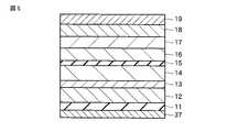
図5に、MTJ素子38の詳細な断面構造を示す。図5に示すように、多結晶金属下地配線37上にはMgO層11が形成され、このMgO層11上にはbcc構造を有する強磁性層12、bcc構造を有するCr層13が順次形成されている。Cr層13上には、ホイスラー合金層14(記録層)、トンネルバリア層(例えば、MgO層)15、ホイスラー合金層16が順次形成されている。さらに、ホイスラー合金層16上には、トップ固定層とするために、強磁性層(例えば、CoFe層)17、反強磁性層18、キャップ層19が順次形成されている。なお、MgO層11は(001)配向していることが望ましい。 FIG. 5 shows a detailed cross-sectional structure of the
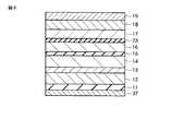
また、MTJ素子38は、図6に示すようなデュアル固定層構造としてもよい。多結晶金属下地配線37上に、MgO層11、bcc構造を有する強磁性層12、bcc構造を有するCr層13、ホイスラー合金層14、トンネルバリア層15、ホイスラー合金層16(記録層)が順次形成されている。さらに、ホイスラー合金層16上に、トンネルバリア層(例えば、MgO層)23、強磁性層17、反強磁性層18、キャップ層19が順次形成されている。強磁性層12、ホイスラー合金層14をピン層とするためには、これらに保持力の強い磁性層を用いるなどすればよい。強磁性層12とホイスラー合金層14との間にCr層13を介して反強磁性結合を形成しても良い。その他、MgO層11と強磁性層12との間に反強磁性層を設けたり、MgO層11の代わりに反強磁性層を用いることができる。 The
さらに、MTJ素子38をトップ固定層として形成した場合を図5に示したが、図7に示すように、ボトム固定層として形成してもよい。すなわち、多結晶金属下地配線37上に、反強磁性層18、bcc構造を有する強磁性層17、bcc構造を有するCr層13、エピタキシャル成長したホイスラー合金層14、トンネルバリア層15、ホイスラー合金層16(記録層)、キャップ層19を順次積層したMTJ構造であってもよい。強磁性層17とホイスラー合金層14との間にCr層13を介して反強磁性結合を形成することもできる。多結晶金属下地配線37と反強磁性層18の間にはMgO層を設けることも可能である。また、多結晶金属下地配線37には、AlまたはAu、Ag、Pt、Cu、Cr等の材料を用いることができ、その他ポリシリコン等の半導体材料などを下地配線として用いてもよい。さらに、図5、図6及び図7において、ホイスラー合金層16は、強磁性層、例えばFe−Co、Fe−Co−Bであってもよい。 Furthermore, although the case where the
第4実施形態によれば、規則性の高い結晶構造を持つホイスラー合金を用いたトンネル磁気抵抗効果素子を形成することができる。これにより、TMR比が高いトンネル磁気抵抗効果素子を備えたMRAMを提供することが可能である。 According to the fourth embodiment, a tunnel magnetoresistive effect element using a Heusler alloy having a highly regular crystal structure can be formed. As a result, it is possible to provide an MRAM including a tunnel magnetoresistive effect element having a high TMR ratio.
[第5実施形態]
次に、本発明の第5実施形態のTMRヘッドについて説明する。このTMRヘッドは、MTJ素子を用いて形成されており、ハードディスクドライブ(HDD)に使用される。図8は、第5実施形態のTMRヘッドの構成を示す断面図である。[Fifth Embodiment]
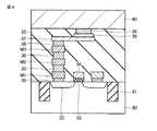
Next, a TMR head according to a fifth embodiment of the invention will be described. This TMR head is formed using an MTJ element and is used in a hard disk drive (HDD). FIG. 8 is a cross-sectional view showing the configuration of the TMR head of the fifth embodiment.
このTMRヘッドは、図8に示すように、MTJ素子が下部電極層41と上部電極層42の間に配置された構造を有している。ここでMTJ素子は、下部電極層41上に、アモルファス層(金属アモルファス層または絶縁体アモルファス層)20、MgO層11、bcc構造を有する強磁性層12、bcc構造を有するCr層13、エピタキシャル成長したホイスラー合金層14、トンネルバリア層15、ホイスラー合金層16を順次積層した構造を有している。強磁性層12とホイスラー合金層14との間にはCr層13を介して反強磁性結合が形成されていても良い。 As shown in FIG. 8, the TMR head has a structure in which an MTJ element is disposed between a
詳述すると、図8に示すように、下部電極層(磁気シールド層)41上には、アモルファス層20、MgO層11、強磁性層12、Cr層13、ホイスラー合金層14、トンネルバリア層(例えば、MgO層)15、ホイスラー合金層16、強磁性層(例えば、CoFe層)17、反強磁性層18、キャップ層19が順次形成されている。さらに、キャップ層19上には、上部電極層(磁気シールド層)42が形成されている。下部電極層41と上部電極層42の間には絶縁膜24が形成されている。なお、MgO層11は(001)配向していることが望ましい。また、ホイスラー合金層16は、強磁性層、例えばFe−Co、Fe−Co−Bであってもよい。 More specifically, as shown in FIG. 8, on the lower electrode layer (magnetic shield layer) 41, the
以上に説明した第4、5実施形態において、bcc構造を有する強磁性層12としては、Fe(鉄)またはFe−Co(鉄コバルト)、Fe−Mn(鉄マンガン)、または前記Fe、Fe−Co、Fe−Mnに、V(バナジウム)、Nb(ニオブ)、Mo(モリブデン)、Ta(タンタル)、Ni(ニッケル)、W(タングステン)の少なくともいずれかを含む合金、またはこれら強磁性体の積層構造を用いることができる。また、bcc構造を有した強磁性層12の格子定数により、ホイスラー合金の格子定数を調整するために、bcc構造を有するCr層13の膜厚は3nm以下が好ましい。また、下部電極層41上のアモルファス層20とMgO層11の膜厚は、キャリアがトンネル可能な膜厚が望ましい。アモルファス層20が導電体の場合は、MgO層11の膜厚がキャリアのトンネル可能な3nm以下であることが望ましく、アモルファス層20が絶縁体の場合は、アモルファス層20とMgO層11とを合せた膜厚が3nm以下であることが望ましい
MTJ素子においてトンネルバリア層となる絶縁体層には、MgOまたはAl2O3を用いることができる。MTJ素子におけるトンネルバリア層の膜厚は、キャリアのスピン緩和が起こらず、かつキャリアがトンネル可能な膜厚が望ましく、スピン拡散長より十分小さい3nm以下が望ましい。In the fourth and fifth embodiments described above, as the
第5実施形態によれば、規則性の高い結晶構造を持つホイスラー合金を用いたトンネル磁気抵抗効果素子を形成することができる。これにより、TMR比が高いトンネル磁気抵抗効果素子を備えたTMRヘッドを提供することが可能である。 According to the fifth embodiment, a tunnel magnetoresistive effect element using a Heusler alloy having a highly regular crystal structure can be formed. Thereby, it is possible to provide a TMR head including a tunnel magnetoresistive effect element having a high TMR ratio.
以下に、比較例及び実施例を参照して本発明の実施形態をさらに詳細に説明する。 Hereinafter, embodiments of the present invention will be described in more detail with reference to comparative examples and examples.
比較例として、ホイスラー合金を有するトンネル磁気抵抗効果素子を作製した。その作製手順を以下に示す。図9は、比較例のトンネル磁気抵抗効果素子の構成を示す断面図である。 As a comparative example, a tunnel magnetoresistive element having a Heusler alloy was produced. The production procedure is shown below. FIG. 9 is a cross-sectional view showing a configuration of a tunnel magnetoresistive effect element of a comparative example.
まず、(001)配向したMgO基板11のスパッタクリーニングを行い、MgO基板11の表面をクリーニングする。次に、MgO基板11上に、スパッタ法によりbcc構造を有する強磁性層(CoFe層)43を膜厚20nm形成する。さらに、強磁性層43上に、スパッタ法によりCo2FeAl0.5Si0.5からなるホイスラー合金層14を膜厚30nm、トンネルバリア層(MgO層)15を膜厚1nm、Co2FeAl0.5Si0.5からなるホイスラー合金層16を膜厚5nm順次形成した。さらに、交換結合磁界を付与するため、ホイスラー合金層16上に、反強磁性層(IrMn層)44を膜厚10nm形成し、反強磁性層44上にキャップ層(Ru層)45を膜厚7nm形成した。上記の手順で作製した比較例のトンネル磁気抵抗効果素子に対して、成膜後に真空中で400℃のアニール処理を行った。First, the (001) -oriented
CIPT(Current In-plane Technique)装置を用いて、作製したトンネル磁気抵抗効果素子の磁気抵抗を測定したところ、TMR比=15.6%と非常に小さい値を示した。また、図9に示したトンネル磁気抵抗効果素子において、CoFe層43の代わりにFe層を用いた場合でもTMR比は小さい値を示した。 When the magnetoresistance of the produced tunnel magnetoresistive effect element was measured using a CIPT (Current In-plane Technique) apparatus, it showed a very small value of TMR ratio = 15.6%. In the tunnel magnetoresistive effect element shown in FIG. 9, even when the Fe layer was used instead of the
そこで次に、本発明の実施例として、図10に示すトンネル磁気抵抗効果素子を作製した。その作製手順を以下に示す。図10は、実施例のトンネル磁気抵抗効果素子の構造を示す断面図である。 Therefore, as an example of the present invention, a tunnel magnetoresistive element shown in FIG. 10 was produced. The production procedure is shown below. FIG. 10 is a cross-sectional view showing the structure of the tunnel magnetoresistive element of the example.
図10に示す実施例のトンネル磁気抵抗効果素子は、図9に示した構造において、bcc構造を有するCoFe層43とCo2FeAl0.5Si0.5からなるホイスラー合金層14との界面にCr層13を膜厚1nm形成した構造を有している。Cr層13を用いることで、MTJ素子におけるホイスラー合金層14とトンネルバリア層15との界面のラフネスを低減させることができる。このような構造を持つトンネル磁気抵抗効果素子を成膜した後、真空中で400℃のアニール処理を行った。The tunnel magnetoresistive element of the embodiment shown in FIG. 10 has an interface between the
CIPT(Current In-plane Technique)装置を用いて、実施例のトンネル磁気抵抗効果素子の磁気抵抗を測定したところ、TMR比=116.0%と高い値を示した。 Using a CIPT (Current In-plane Technique) apparatus, the magnetoresistance of the tunnel magnetoresistive element of the example was measured, and the TMR ratio was 116.0%, which was a high value.
また、形成されたホイスラー合金の結晶構造を、X線回折装置において評価した結果を図11に示す。図11より、形成されているホイスラー合金は(002)ピークを観測していることから、B2構造であることがわかる。また、bcc構造を有するCoFe層43とCo2FeAl0.5Si0.5からなるホイスラー合金層14との界面にCr層13を膜厚1nm形成しても、ホイスラー合金層14はB2構造を保ち、さらに格子定数の変化も無いことがわかる。よって、bcc構造を有する強磁性層とホイスラー合金層との界面に、膜厚が薄いCr層を形成することにより、bcc構造を有した強磁性層の格子定数を引き摺ったホイスラー合金が形成できることが明らかとなった。なお、図11中のCFASは、Co2FeAl0.5Si0.5からなるホイスラー合金を表す。また、CFAS(30)/Cr(1)/CoFe(20)等の記載は、CoFe層(膜厚20nm)上に、Cr層(膜厚1nm)、Co2FeAl0.5Si0.5からなるホイスラー合金(膜厚30nm)を順次形成した構造であることを表す。Moreover, the result of having evaluated the crystal structure of the formed Heusler alloy in the X-ray-diffraction apparatus is shown in FIG. FIG. 11 shows that the formed Heusler alloy has a (002) peak, and thus has a B2 structure. Even if the
また、図10に示した構造において、bcc構造を有するCoFe層43の代わりに、bcc構造を有するCr層/bcc構造を有するCoFe層を形成した。詳述すると、MgO基板11上にbcc構造を有するCr層を形成し、このCr層上にbcc構造を有するCoFe層を形成した。このCoFe層上にはCr層13が形成されている。このような構造を有するトンネル磁気抵抗効果素子では、TMR比が更に向上することが明らかとなった。これより、bcc構造を有する強磁性層は、上記元素を一部その他の元素で置換してもbcc構造が保たれていればよく、その場合にも強磁性層上のホイスラー合金の結晶性、ひいては磁気的特性などが良好なものとなる。また、前記強磁性層は、積層構造を形成していてもよい。 Further, in the structure shown in FIG. 10, instead of the
以上のことから、本発明の実施例によれば、規則性の高い結晶構造を持つホイスラー合金を形成でき、かつ高いTMR比を持つトンネル磁気抵抗効果素子を実現できることが明らかとなった。本実施例の図10に示した構造を半導体基板上に形成すれば、bcc構造を有する強磁性層から、スピンの自由度を付加したキャリアを半導体基板中に伝導させることが可能である。 From the above, according to the example of the present invention, it has become clear that a Heusler alloy having a highly ordered crystal structure can be formed and a tunnel magnetoresistive element having a high TMR ratio can be realized. If the structure shown in FIG. 10 of this embodiment is formed on a semiconductor substrate, carriers added with a degree of freedom of spin can be conducted from the ferromagnetic layer having the bcc structure into the semiconductor substrate.
また、前述した各実施形態はそれぞれ、単独で実施できるばかりでなく、適宜組み合わせて実施することも可能である。さらに、前述した各実施形態には種々の段階の発明が含まれており、各実施形態において開示した複数の構成要件の適宜な組み合わせにより、種々の段階の発明を抽出することも可能である。 In addition, each of the above-described embodiments can be implemented not only independently but also in an appropriate combination. Furthermore, the above-described embodiments include inventions at various stages, and the inventions at various stages can be extracted by appropriately combining a plurality of constituent elements disclosed in the embodiments.
10…半導体単結晶基板、10A…不純物拡散層、11…MgO層、12…強磁性層、13…Cr層、14…ホイスラー合金層、15…トンネルバリア層、16…ホイスラー合金層、17…強磁性層、18…反強磁性層、19…キャップ層、20…アモルファス層、21…ゲート絶縁膜、22…ゲート電極、23…トンネルバリア層、24…絶縁膜、30…半導体単結晶基板、31…素子分離領域、32…ソース領域(またはドレイン領域)、33…ゲート絶縁膜、34…ゲート電極、35…層間絶縁膜、36…コンタクトプラグ、37…多結晶金属下地配線、38…MTJ素子、39…金属ビア(または金属ハードマスク)、40…ビット線、41…下部電極層(磁気シールド層)、42…上部電極層(磁気シールド層)、43…強磁性層(CoFe層)、44…反強磁性層(IrMn層)、45…キャップ層(Ru層)、M1…第1配線、M2…第2配線、M3…第3配線。 DESCRIPTION OF
Claims (5)
Translated fromJapanese前記MgO層上に形成された体心立方格子構造を有する第1強磁性層と、
前記第1強磁性層上に形成された体心立方格子構造を有する、膜厚が3nm以下であるCr層と、
前記Cr層上に形成され、B2構造またはL21構造を有するホイスラー合金層と、
を含む構造をソース及びドレインに具備することを特徴とするスピンMOS電界効果トランジスタ。An MgO layer formed on a semiconductor substrate;
A first ferromagnetic layer having a body-centered cubic lattice structure formed on the MgO layer;
A Cr layer having a body-centered cubic lattice structure formed on the first ferromagnetic layer and having a thickness of 3 nm or less;
A Heusler alloy layer formed on the Cr layer and having a B2 structure or an L21 structure;
A spin MOS field-effect transistor comprising a source and a drain having a structure including:
前記MgO層上に形成された体心立方格子構造を有する第1強磁性層と、
前記第1強磁性層上に形成された体心立方格子構造を有する、膜厚が3nm以下であるCr層と、
前記Cr層上に形成され、B2構造またはL21構造を有するホイスラー合金層と、
前記ホイスラー合金層上に形成されたバリア層と、
前記バリア層上に形成された第2強磁性層と、
を含む構造を少なくともソースまたはドレインのいずれかに具備することを特徴とするスピンMOS電界効果トランジスタ。An MgO layer formed on a semiconductor substrate;
A first ferromagnetic layer having a body-centered cubic lattice structure formed on the MgO layer;
A Cr layer having a body-centered cubic lattice structure formed on the first ferromagnetic layer and having a thickness of 3 nm or less;
A Heusler alloy layer formed on the Cr layer and having a B2 structure or an L21 structure;
A barrier layer formed on the Heusler alloy layer;
A second ferromagnetic layer formed on the barrier layer;
A spin MOS field-effect transistor comprising at least one of a source and a drain having a structure including:
Priority Applications (3)
| Application Number | Priority Date | Filing Date | Title |
|---|---|---|---|
| JP2008005041AJP4703660B2 (en) | 2008-01-11 | 2008-01-11 | Spin MOS field effect transistor |
| US12/342,383US8243400B2 (en) | 2008-01-11 | 2008-12-23 | Tunneling magnetoresistive effect element and spin MOS field-effect transistor |
| US13/533,198US8335059B2 (en) | 2008-01-11 | 2012-06-26 | Tunneling magnetoresistive effect element and spin MOS field-effect |
Applications Claiming Priority (1)
| Application Number | Priority Date | Filing Date | Title |
|---|---|---|---|
| JP2008005041AJP4703660B2 (en) | 2008-01-11 | 2008-01-11 | Spin MOS field effect transistor |
Publications (2)
| Publication Number | Publication Date |
|---|---|
| JP2009170556A JP2009170556A (en) | 2009-07-30 |
| JP4703660B2true JP4703660B2 (en) | 2011-06-15 |
Family
ID=40850422
Family Applications (1)
| Application Number | Title | Priority Date | Filing Date |
|---|---|---|---|
| JP2008005041AExpired - Fee RelatedJP4703660B2 (en) | 2008-01-11 | 2008-01-11 | Spin MOS field effect transistor |
Country Status (2)
| Country | Link |
|---|---|
| US (2) | US8243400B2 (en) |
| JP (1) | JP4703660B2 (en) |
Families Citing this family (32)
| Publication number | Priority date | Publication date | Assignee | Title |
|---|---|---|---|---|
| JP4580966B2 (en)* | 2007-08-24 | 2010-11-17 | 株式会社東芝 | Laminated body having Heusler alloy, spin MOS field effect transistor and tunnel magnetoresistive element using the laminated body |
| JP4703660B2 (en)* | 2008-01-11 | 2011-06-15 | 株式会社東芝 | Spin MOS field effect transistor |
| JP4762285B2 (en)* | 2008-09-24 | 2011-08-31 | 株式会社東芝 | Spin transistor, integrated circuit, and magnetic memory |
| JP4764466B2 (en) | 2008-09-25 | 2011-09-07 | 株式会社東芝 | Laminated body having Heusler alloy, magnetoresistive element using this laminated body, and spin transistor |
| JP4908540B2 (en) | 2009-03-25 | 2012-04-04 | 株式会社東芝 | Spin MOSFET and reconfigurable logic circuit |
| JP5527669B2 (en)* | 2009-05-22 | 2014-06-18 | 独立行政法人物質・材料研究機構 | Ferromagnetic tunnel junction and magnetoresistive effect element using the same |
| WO2011033665A1 (en)* | 2009-09-18 | 2011-03-24 | 株式会社 東芝 | Semiconductor device and method for manufacturing same |
| US8766341B2 (en)* | 2009-10-20 | 2014-07-01 | The Regents Of The University Of California | Epitaxial growth of single crystalline MgO on germanium |
| JP5338714B2 (en)* | 2010-02-24 | 2013-11-13 | Tdk株式会社 | Magnetic sensor, magnetic detection device, and magnetic head |
| JP2012039010A (en) | 2010-08-10 | 2012-02-23 | Tdk Corp | Magnetic sensor and magnetic detection apparatus |
| JP5651826B2 (en)* | 2010-09-03 | 2015-01-14 | Tdk株式会社 | Spin injection electrode structure, spin transport device, and spin transport device |
| JP5786341B2 (en) | 2010-09-06 | 2015-09-30 | ソニー株式会社 | Memory element and memory device |
| US9880232B2 (en) | 2012-03-14 | 2018-01-30 | Seagate Technology Llc | Magnetic sensor manufacturing |
| JP5649605B2 (en) | 2012-03-26 | 2015-01-07 | 株式会社東芝 | Spin transistor and memory |
| JP5959313B2 (en)* | 2012-05-28 | 2016-08-02 | 三菱電機株式会社 | Magnetoresistive element, magnetic field detector and physical quantity detector |
| JP5777588B2 (en)* | 2012-09-21 | 2015-09-09 | 株式会社東芝 | Magnetoresistive effect element |
| JP6148450B2 (en)* | 2012-10-29 | 2017-06-14 | 株式会社東芝 | Stacked structure, spin transistor and reconfigurable logic circuit |
| US9034491B2 (en)* | 2012-11-30 | 2015-05-19 | Seagate Technology Llc | Low resistance area magnetic stack |
| JP2014146405A (en)* | 2013-01-30 | 2014-08-14 | Toshiba Corp | Magnetoresistance effect magnetic head and magnetic recording/reproducing device |
| US9461242B2 (en) | 2013-09-13 | 2016-10-04 | Micron Technology, Inc. | Magnetic memory cells, methods of fabrication, semiconductor devices, memory systems, and electronic systems |
| US9608197B2 (en) | 2013-09-18 | 2017-03-28 | Micron Technology, Inc. | Memory cells, methods of fabrication, and semiconductor devices |
| JP2015061045A (en)* | 2013-09-20 | 2015-03-30 | 株式会社東芝 | Spin-based mosfet |
| US9236564B2 (en) | 2013-12-11 | 2016-01-12 | Samsung Electronics Co., Ltd. | Method and system for providing an engineered magnetic layer including Heusler layers and an amorphous insertion layer |
| US10454024B2 (en) | 2014-02-28 | 2019-10-22 | Micron Technology, Inc. | Memory cells, methods of fabrication, and memory devices |
| US9281466B2 (en) | 2014-04-09 | 2016-03-08 | Micron Technology, Inc. | Memory cells, semiconductor structures, semiconductor devices, and methods of fabrication |
| US9269888B2 (en) | 2014-04-18 | 2016-02-23 | Micron Technology, Inc. | Memory cells, methods of fabrication, and semiconductor devices |
| US9349945B2 (en) | 2014-10-16 | 2016-05-24 | Micron Technology, Inc. | Memory cells, semiconductor devices, and methods of fabrication |
| US9768377B2 (en) | 2014-12-02 | 2017-09-19 | Micron Technology, Inc. | Magnetic cell structures, and methods of fabrication |
| US10439131B2 (en) | 2015-01-15 | 2019-10-08 | Micron Technology, Inc. | Methods of forming semiconductor devices including tunnel barrier materials |
| JP2016178254A (en) | 2015-03-20 | 2016-10-06 | 株式会社東芝 | Spin transistor memory |
| KR102175385B1 (en) | 2016-04-12 | 2020-11-06 | 에스케이하이닉스 주식회사 | Multilayered magnetic thin film stack and data storage device having the same |
| WO2018004700A1 (en)* | 2016-07-01 | 2018-01-04 | Intel Corporation | Transistors with metal source and drain contacts including a heusler alloy |
Family Cites Families (19)
| Publication number | Priority date | Publication date | Assignee | Title |
|---|---|---|---|---|
| JP3629057B2 (en) | 1995-03-14 | 2005-03-16 | 株式会社東芝 | Method for manufacturing Heusler alloy thin film, laminated film provided with magnetic film, magnetoresistive effect element and solid-state magnetic recording element using the same |
| JP3621367B2 (en)* | 2001-09-17 | 2005-02-16 | 株式会社東芝 | Spin transistor |
| EP1737055B1 (en)* | 2004-03-12 | 2012-01-11 | Japan Science and Technology Agency | Magnetoresistive element and its manufacturing method |
| JP4744934B2 (en)* | 2004-06-16 | 2011-08-10 | 株式会社東芝 | Spin transistor |
| JP2006073861A (en)* | 2004-09-03 | 2006-03-16 | Renesas Technology Corp | Magnetic storage device |
| JP4373938B2 (en)* | 2005-02-17 | 2009-11-25 | 株式会社東芝 | Magnetic random access memory |
| JP2006295001A (en)* | 2005-04-13 | 2006-10-26 | Sony Corp | Storage element and memory |
| JP2007092147A (en)* | 2005-09-29 | 2007-04-12 | Tokyo Institute Of Technology | Multilayer structure, semiconductor device, and transistor |
| JP2007150265A (en)* | 2005-10-28 | 2007-06-14 | Toshiba Corp | Magnetoresistive element and magnetic storage device |
| JP4582488B2 (en)* | 2006-04-27 | 2010-11-17 | 独立行政法人科学技術振興機構 | Magnetic thin film, magnetoresistive effect element and magnetic device using the same |
| JP4455558B2 (en)* | 2006-09-08 | 2010-04-21 | 株式会社東芝 | Spin MOSFET |
| JP4580966B2 (en)* | 2007-08-24 | 2010-11-17 | 株式会社東芝 | Laminated body having Heusler alloy, spin MOS field effect transistor and tunnel magnetoresistive element using the laminated body |
| JP4496242B2 (en) | 2007-08-29 | 2010-07-07 | 株式会社東芝 | Spin transistor and magnetic memory |
| JP5082688B2 (en)* | 2007-08-30 | 2012-11-28 | Tdk株式会社 | Spin transistor and semiconductor memory |
| US7936028B2 (en)* | 2007-11-09 | 2011-05-03 | Samsung Electronics Co., Ltd. | Spin field effect transistor using half metal and method of manufacturing the same |
| JP4703660B2 (en)* | 2008-01-11 | 2011-06-15 | 株式会社東芝 | Spin MOS field effect transistor |
| JP2009239122A (en)* | 2008-03-27 | 2009-10-15 | Toshiba Corp | Magneto-resistance effect device and spin mos (metal oxide semiconductor) field-effect transistor |
| JP4764466B2 (en) | 2008-09-25 | 2011-09-07 | 株式会社東芝 | Laminated body having Heusler alloy, magnetoresistive element using this laminated body, and spin transistor |
| JP4738499B2 (en)* | 2009-02-10 | 2011-08-03 | 株式会社東芝 | Manufacturing method of spin transistor |
- 2008
- 2008-01-11JPJP2008005041Apatent/JP4703660B2/ennot_activeExpired - Fee Related
- 2008-12-23USUS12/342,383patent/US8243400B2/ennot_activeExpired - Fee Related
- 2012
- 2012-06-26USUS13/533,198patent/US8335059B2/ennot_activeExpired - Fee Related
Also Published As
| Publication number | Publication date |
|---|---|
| US20090180215A1 (en) | 2009-07-16 |
| US8335059B2 (en) | 2012-12-18 |
| US8243400B2 (en) | 2012-08-14 |
| US20120273856A1 (en) | 2012-11-01 |
| JP2009170556A (en) | 2009-07-30 |
Similar Documents
| Publication | Publication Date | Title |
|---|---|---|
| JP4703660B2 (en) | Spin MOS field effect transistor | |
| JP4580966B2 (en) | Laminated body having Heusler alloy, spin MOS field effect transistor and tunnel magnetoresistive element using the laminated body | |
| US11569441B2 (en) | Maintaining coercive field after high temperature anneal for magnetic device applications with perpendicular magnetic anistropy | |
| JP4455558B2 (en) | Spin MOSFET | |
| JP6464516B2 (en) | Magnetic cell structure and method of manufacture | |
| KR101929583B1 (en) | Nonvolatile magnetic memory device | |
| US8592927B2 (en) | Multilayers having reduced perpendicular demagnetizing field using moment dilution for spintronic applications | |
| JP4496242B2 (en) | Spin transistor and magnetic memory | |
| US20220238799A1 (en) | Magnetoresistive element having a composite recording structure | |
| US20230039108A1 (en) | Perpendicular mtj element having a soft-magnetic adjacent layer and methods of making the same | |
| JP5144569B2 (en) | Spin transistor and logic circuit device | |
| JP4997194B2 (en) | Spin transistor and reconfigurable logic circuit | |
| JP2009239122A (en) | Magneto-resistance effect device and spin mos (metal oxide semiconductor) field-effect transistor | |
| JP4599285B2 (en) | Field effect transistor, integrated circuit, and memory | |
| US11910721B2 (en) | Perpendicular MTJ element having a cube-textured reference layer and methods of making the same | |
| JP5377531B2 (en) | Spin MOS field effect transistor | |
| US20220246836A1 (en) | Composite recording structure for an improved write profermance | |
| US10867651B2 (en) | Initialization process for magnetic random access memory (MRAM) production | |
| WO2011062005A1 (en) | Ferromagnetic tunnel junction element | |
| JP6986729B2 (en) | Single crystal magnetoresistive element and devices using it | |
| JP5072877B2 (en) | Spin transistor |
Legal Events
| Date | Code | Title | Description |
|---|---|---|---|
| A977 | Report on retrieval | Free format text:JAPANESE INTERMEDIATE CODE: A971007 Effective date:20091106 | |
| A131 | Notification of reasons for refusal | Free format text:JAPANESE INTERMEDIATE CODE: A131 Effective date:20091117 | |
| A521 | Request for written amendment filed | Free format text:JAPANESE INTERMEDIATE CODE: A523 Effective date:20100118 | |
| A131 | Notification of reasons for refusal | Free format text:JAPANESE INTERMEDIATE CODE: A131 Effective date:20100629 | |
| A521 | Request for written amendment filed | Free format text:JAPANESE INTERMEDIATE CODE: A523 Effective date:20100830 | |
| TRDD | Decision of grant or rejection written | ||
| A01 | Written decision to grant a patent or to grant a registration (utility model) | Free format text:JAPANESE INTERMEDIATE CODE: A01 Effective date:20110215 | |
| A61 | First payment of annual fees (during grant procedure) | Free format text:JAPANESE INTERMEDIATE CODE: A61 Effective date:20110308 | |
| R151 | Written notification of patent or utility model registration | Ref document number:4703660 Country of ref document:JP Free format text:JAPANESE INTERMEDIATE CODE: R151 | |
| LAPS | Cancellation because of no payment of annual fees |