JP4701691B2 - Etching method - Google Patents
Etching methodDownload PDFInfo
- Publication number
- JP4701691B2 JP4701691B2JP2004344608AJP2004344608AJP4701691B2JP 4701691 B2JP4701691 B2JP 4701691B2JP 2004344608 AJP2004344608 AJP 2004344608AJP 2004344608 AJP2004344608 AJP 2004344608AJP 4701691 B2JP4701691 B2JP 4701691B2
- Authority
- JP
- Japan
- Prior art keywords
- gas
- etching
- containing gas
- nitrogen
- flow rate
- Prior art date
- Legal status (The legal status is an assumption and is not a legal conclusion. Google has not performed a legal analysis and makes no representation as to the accuracy of the status listed.)
- Expired - Fee Related
Links
Images


Classifications
- H—ELECTRICITY
- H01—ELECTRIC ELEMENTS
- H01L—SEMICONDUCTOR DEVICES NOT COVERED BY CLASS H10
- H01L21/00—Processes or apparatus adapted for the manufacture or treatment of semiconductor or solid state devices or of parts thereof
- H01L21/02—Manufacture or treatment of semiconductor devices or of parts thereof
- H01L21/04—Manufacture or treatment of semiconductor devices or of parts thereof the devices having potential barriers, e.g. a PN junction, depletion layer or carrier concentration layer
- H01L21/18—Manufacture or treatment of semiconductor devices or of parts thereof the devices having potential barriers, e.g. a PN junction, depletion layer or carrier concentration layer the devices having semiconductor bodies comprising elements of Group IV of the Periodic Table or AIIIBV compounds with or without impurities, e.g. doping materials
- H01L21/30—Treatment of semiconductor bodies using processes or apparatus not provided for in groups H01L21/20 - H01L21/26
- H01L21/302—Treatment of semiconductor bodies using processes or apparatus not provided for in groups H01L21/20 - H01L21/26 to change their surface-physical characteristics or shape, e.g. etching, polishing, cutting
- H01L21/306—Chemical or electrical treatment, e.g. electrolytic etching
- H01L21/3065—Plasma etching; Reactive-ion etching
- C—CHEMISTRY; METALLURGY
- C23—COATING METALLIC MATERIAL; COATING MATERIAL WITH METALLIC MATERIAL; CHEMICAL SURFACE TREATMENT; DIFFUSION TREATMENT OF METALLIC MATERIAL; COATING BY VACUUM EVAPORATION, BY SPUTTERING, BY ION IMPLANTATION OR BY CHEMICAL VAPOUR DEPOSITION, IN GENERAL; INHIBITING CORROSION OF METALLIC MATERIAL OR INCRUSTATION IN GENERAL
- C23F—NON-MECHANICAL REMOVAL OF METALLIC MATERIAL FROM SURFACE; INHIBITING CORROSION OF METALLIC MATERIAL OR INCRUSTATION IN GENERAL; MULTI-STEP PROCESSES FOR SURFACE TREATMENT OF METALLIC MATERIAL INVOLVING AT LEAST ONE PROCESS PROVIDED FOR IN CLASS C23 AND AT LEAST ONE PROCESS COVERED BY SUBCLASS C21D OR C22F OR CLASS C25
- C23F4/00—Processes for removing metallic material from surfaces, not provided for in group C23F1/00 or C23F3/00
- H—ELECTRICITY
- H01—ELECTRIC ELEMENTS
- H01J—ELECTRIC DISCHARGE TUBES OR DISCHARGE LAMPS
- H01J37/00—Discharge tubes with provision for introducing objects or material to be exposed to the discharge, e.g. for the purpose of examination or processing thereof
- H01J37/32—Gas-filled discharge tubes
- H01J37/32009—Arrangements for generation of plasma specially adapted for examination or treatment of objects, e.g. plasma sources
- H01J37/32192—Microwave generated discharge
- H—ELECTRICITY
- H01—ELECTRIC ELEMENTS
- H01L—SEMICONDUCTOR DEVICES NOT COVERED BY CLASS H10
- H01L21/00—Processes or apparatus adapted for the manufacture or treatment of semiconductor or solid state devices or of parts thereof
- H01L21/02—Manufacture or treatment of semiconductor devices or of parts thereof
- H01L21/04—Manufacture or treatment of semiconductor devices or of parts thereof the devices having potential barriers, e.g. a PN junction, depletion layer or carrier concentration layer
- H01L21/18—Manufacture or treatment of semiconductor devices or of parts thereof the devices having potential barriers, e.g. a PN junction, depletion layer or carrier concentration layer the devices having semiconductor bodies comprising elements of Group IV of the Periodic Table or AIIIBV compounds with or without impurities, e.g. doping materials
- H01L21/30—Treatment of semiconductor bodies using processes or apparatus not provided for in groups H01L21/20 - H01L21/26
- H01L21/31—Treatment of semiconductor bodies using processes or apparatus not provided for in groups H01L21/20 - H01L21/26 to form insulating layers thereon, e.g. for masking or by using photolithographic techniques; After treatment of these layers; Selection of materials for these layers
- H01L21/3205—Deposition of non-insulating-, e.g. conductive- or resistive-, layers on insulating layers; After-treatment of these layers
- H01L21/321—After treatment
- H01L21/3213—Physical or chemical etching of the layers, e.g. to produce a patterned layer from a pre-deposited extensive layer
- H01L21/32133—Physical or chemical etching of the layers, e.g. to produce a patterned layer from a pre-deposited extensive layer by chemical means only
- H01L21/32135—Physical or chemical etching of the layers, e.g. to produce a patterned layer from a pre-deposited extensive layer by chemical means only by vapour etching only
- H01L21/32136—Physical or chemical etching of the layers, e.g. to produce a patterned layer from a pre-deposited extensive layer by chemical means only by vapour etching only using plasmas
Landscapes
- Engineering & Computer Science (AREA)
- Chemical & Material Sciences (AREA)
- Physics & Mathematics (AREA)
- Plasma & Fusion (AREA)
- Condensed Matter Physics & Semiconductors (AREA)
- Power Engineering (AREA)
- Microelectronics & Electronic Packaging (AREA)
- Computer Hardware Design (AREA)
- Manufacturing & Machinery (AREA)
- General Physics & Mathematics (AREA)
- Materials Engineering (AREA)
- General Chemical & Material Sciences (AREA)
- Chemical Kinetics & Catalysis (AREA)
- Organic Chemistry (AREA)
- Metallurgy (AREA)
- Mechanical Engineering (AREA)
- Analytical Chemistry (AREA)
- Drying Of Semiconductors (AREA)
- Internal Circuitry In Semiconductor Integrated Circuit Devices (AREA)
- Electrodes Of Semiconductors (AREA)
- ing And Chemical Polishing (AREA)
Description
Translated fromJapanese本発明は、半導体ウエハ等の被処理体の表面にプラズマにより活性化されたエッチングガスを用いてエッチング処理を施すエッチング方法に関する。The present invention isrelated to etchinggrayed method for performing an etching process using a surface activated etching gas by the plasma of the object to be processed such as a semiconductor wafer.
一般に、半導体製品の集積回路を形成するには、半導体ウエハ等の被処理体に対して、成膜処理、改質処理、酸化拡散処理、エッチング処理等の各種の処理を行うが、近年の半導体集積回路の更なる高密度化、高微細化、薄膜化及び製品歩留まり向上の要請に応じて、エッチング処理時においても、下地層との選択性を高く維持しつつエッチング形状を崩すことなくこの形状を設計通りに精度良く維持することが求められている。
一般に、エッチング処理を行う場合には、エッチング対象層とその下層に位置するエッチングストッパ層となる下地層との選択性を考慮してエッチングガスが選定され、また、このエッチング処理を行う時には低温で処理ができ、且つエッチング効率を高めるためにプラズマを用いる傾向にある(特許文献1及び2)。In general, in order to form an integrated circuit of a semiconductor product, various processes such as a film forming process, a modification process, an oxidation diffusion process, and an etching process are performed on an object to be processed such as a semiconductor wafer. In response to demands for higher density, higher miniaturization, thinner film, and higher product yield in integrated circuits, this shape is maintained without breaking the etching shape while maintaining high selectivity with the underlying layer even during the etching process. Is required to be maintained with high accuracy as designed.
In general, when performing an etching process, an etching gas is selected in consideration of the selectivity between an etching target layer and an underlying layer serving as an etching stopper layer positioned below the etching target layer. There is a tendency to use plasma to improve the etching efficiency (
ここで従来のエッチング方法として、例えばゲート電極を形成するためにポリシリコン層上に形成されたタングステン含有膜をパターンエッチングする場合を例にとって説明する。図8は被処理体の一部を示す部分拡大断面図である。図示するように、この被処理体は、例えばシリコン基板等の半導体ウエハよりなり、ここではこの半導体ウエハSの表面にゲート酸化膜となるSiO2 膜2及びシリコン含有材料である例えばポリシリコン層よりなる下地層4が形成されている。そして、更に上記下地層4上にタングステン含有材料よりなるエッチング対象層6が形成されている。このエッチング対象層6は、ここでは例えば下層となる窒化タングステン(WN)膜6Aと上層となるタングステン(W)膜6Bとの積層構造になっている。そして、このように形成された上記エッチング対象層6の上面に例えばゲート電極を形成するためのパターン化されたマスク8が形成されている。このマスク8としては、例えばSiN膜、SiO2 膜、フォトレジスト膜等が用いられる。Here, as a conventional etching method, for example, a case where a tungsten-containing film formed on a polysilicon layer is patterned to form a gate electrode will be described as an example. FIG. 8 is a partially enlarged sectional view showing a part of the object to be processed. As shown in the figure, the object to be processed is made of, for example, a semiconductor wafer such as a silicon substrate. Here, the surface of the semiconductor wafer S is made of an SiO2 film 2 serving as a gate oxide film and a silicon-containing material such as a polysilicon layer. The
さて、上記したような積層構造を有する半導体ウエハSに対してエッチング処理を行う場合には、従来においては、エッチングガスとしてCl2 ガスやNF3 ガスやSF6 ガスを用い、添加ガスとして下地層との選択性を高めるためにO2 ガス等を用いており、これらのガスをプラズマにより活性化させてエッチング処理を行うようになっている。また必要に応じて不活性ガス、例えばArガスも供給される場合もあり、またO2 ガスに代えてN2 ガスを用いる場合もある。
上記したような半導体ウエハSをエッチングする場合、プラズマによりエッチングガスがプラズマ化されて活性化し、発生した活性種がエッチング対象層6をアタックして、この時、エッチング対象層6を形成する材料と活性種や添加ガスとが反応して反応生成物が生成される。そして、反応生成物は気化してガスとなって排出され、結果的に、マスク8によって保護されている部分以外のエッチング対象層は削り取られ、ストッパ層として機能する下地層4の部分でエッチングが停止することになる。When performing an etching process on the semiconductor wafer S having the above-described laminated structure, conventionally, Cl2 gas, NF3 gas, or SF6 gas is used as an etching gas, and an underlayer is used as an additive gas. In order to improve the selectivity, an O2 gas or the like is used, and these gases are activated by plasma to perform an etching process. Further, an inert gas, for example, Ar gas may be supplied as necessary, and N2 gas may be used instead of O2 gas.
When etching the semiconductor wafer S as described above, the etching gas is turned into plasma by plasma and activated, and the generated active species attack the
ところで、エッチング処理時に発生する反応生成物としては種々の物質があり、その一例としてWFやWOCl4 等の反応生成物は比較的揮発性が高いことから問題はないが、エッチングガスとしてCl系ガスを用いた時に発生するWO3 やWClxOy(x,y:正数)等の反応生成物は比較的揮発性が低いことから堆積し易い性質をもっている。
ここで下地層4との選択比を高めるには上記したようにO2 ガスの流量比を増加すればよいが、O2 ガスの流量比を増加すると、上記WO3 やWClxOy等の揮発し難い反応生成物がエッチング部分に付着してエッチング形状が劣化してしまう。また、エッチングガスとしてF系ガスを用いると、このガスは反応性に富むことからエッチング対象層6が過度に削り取られてアンダーカットが生じてエッチング形状が劣化する、という問題があった。By the way, there are various substances as reaction products generated during the etching process. For example, reaction products such as WF and WOCl4 have no problem because they are relatively volatile. Reaction products such as WO3 and WClxOy (x, y: positive numbers) generated when using benzene have a property of being easily deposited because of their relatively low volatility.
Here, increase the selectivity to the
図9はこのエッチング処理時のエッチング形状の一例を示す電子顕微鏡写真とその模式図である。図9(A)はエッチングが適正に行われて適正なエッチング形状が得られた状態の模式図を示し、図9(B)はエッチングガスとしてN2 が添加されたCl2 ガスを用いたときのエッチング形状を示し、側部にWO3 やWClxOy等の不揮発性堆積物10が堆積する現象が発生しており、図9(C)はエッチングガスとしてO2 が添加されたCl2 ガスを用いたときのエッチング形状を示し、側部が円弧状に過度に削り取られてアンダーカット部12が形成される現象が発生している。このように、従来のエッチング方法では図9(B)及び図9(C)に示すようにエッチング形状が劣化する場合があった。また、単にエッチングガスとしてCl2 ガスのみを用いた場合には選択比が極端に低下して下地層であるポリシリコン層が削られてしまう。FIG. 9 is an electron micrograph showing an example of an etching shape at the time of this etching process and a schematic diagram thereof. FIG. 9A is a schematic view showing a state in which etching is properly performed and an appropriate etching shape is obtained, and FIG. 9B is a case where Cl2 gas added with N2 is used as an etching gas. FIG. 9C shows the use of a Cl2 gas to which O2 is added as an etching gas. In FIG. 9C, a
上記したようなエッチング形状の劣化は、線幅等の寸法の設計ルールがそれ程厳しくない従来の場合には、それ程問題にはならなかったが、今日のように微細化が更に進んで寸法の設計ルールがより厳しくなった状況下においては、早期に解決すべき問題である。
本発明は、以上のような問題点に着目し、これを有効に解決すべく創案されたものである。本発明の目的は、下地層に対して高い選択性を維持しつつ、しかも適正なエッチング形状を得ることが可能なエッチング方法を提供することにある。The deterioration of the etching shape as described above was not so much a problem in the conventional case where the design rule of the dimensions such as the line width is not so strict. In a situation where rules are becoming stricter, this is a problem that should be resolved early.
The present invention has been devised to pay attention to the above problems and to effectively solve them. An object of the present invention isto provide an etchingmethod capable of obtaining an appropriate etching shape while maintaining high selectivity with respect to a base layer.
本発明者は、エッチング処理時のエッチングガスと添加ガスについて鋭意研究した結果、タングステン膜や窒化タングステン膜などのタングステン含有材料よりなる薄膜をエッチングする場合には、Cl2 ガスとO2 ガスとN2 ガスとを用いたり、Cl2 ガスとNO等の酸化窒素系ガスとを用いることにより、高い選択性及び適正なエッチング形状が得られることを見い出すことにより、本発明に至ったものである。As a result of intensive studies on the etching gas and additive gas during the etching process, the present inventor has found that when etching a thin film made of a tungsten-containing material such as a tungsten film or a tungsten nitride film, Cl2 gas, O2 gas, and NThe present invention has been achieved by finding that high selectivity and an appropriate etching shape can be obtained by usingtwo gases or by using a Cl2 gas and a nitrogen oxide-based gas such as NO.
請求項1に係る発明は、ポリシリコン層よりなる下地層上に窒化タングステン膜とタングステン膜との積層構造よりなるエッチング対象層が形成された被処理体に対して真空引き可能になされた処理容器内にてプラズマの存在下でエッチング処理を施すようにしたエッチング方法において、前記エッチング時のガスとしてCl2 よりなる塩素含有ガスとO2 よりなる酸素含有ガスとN2 よりなる窒素含有ガスのみとを用いると共に、前記塩素含有ガス及び前記窒素含有ガスの合計流量に対する前記酸素含有ガスの添加量は2.9〜8.6%の範囲内であり、前記塩素含有ガス及び前記窒素含有ガスの合計流量に対する前記窒素含有ガスの流量比は50〜80%の範囲内であるようにしたことを特徴とするエッチング方法である。
このように、エッチング時のガスとして塩素含有ガスと酸素含有ガスと窒素含有ガスとを用いるようにしたので、下地層に対して高い選択性を維持しつつ、しかも適正なエッチング形状を得ることができる。The invention according to
Thus, since chlorine-containing gas, oxygen-containing gas, and nitrogen-containing gas are used as the etching gas, it is possible to obtain an appropriate etching shape while maintaining high selectivity with respect to the underlayer. it can.
本発明の関連技術は、シリコン含有材料よりなる下地層上にタングステン及び/又は窒化タングステンよりなるエッチング対象層が形成された被処理体に対して真空引き可能になされた処理容器内にてプラズマの存在下でエッチング処理を施すようにしたエッチング方法において、前記エッチング時のガスとして塩素含有ガスと酸化窒素系ガスのみとを用いるようにしたことを特徴とするエッチング方法である。
このように、エッチング時のガスとして塩素含有ガスと酸化窒素系ガスとを用いるようにしたので、下地層に対して高い選択性を維持しつつ、しかも適正なエッチング形状を得ることができる。The related art of the present invention is a method in which a plasma is generated in a processing container that can be evacuated with respect to an object to be processed in which an etching target layer made of tungsten and / or tungsten nitride is formed on a base layermade of a silicon-containing material. In the etching method in which the etching treatment is performed in the presence, only a chlorine-containing gas and a nitrogen oxide-based gas are used as the gas during the etching.
Thus, since the chlorine-containing gas and the nitrogen oxide-based gas are used as the etching gas, an appropriate etching shape can be obtained while maintaining high selectivity with respect to the underlayer.
また本発明では、例えば請求項2に規定するように、前記プラズマはマイクロ波によって発生される。
また例えば請求項3に規定するように、前記エッチング処理はRLSA(Radial Line Slot Antenna)方式の平面アンテナ部材を用いた処理容器内で行われる。
本発明の関連技術は、シリコン含有材料よりなる下地層上にタングステン及び/又は窒化タングステンよりなるエッチング対象層が形成された被処理体に対して真空引き可能になされた処理容器内にてプラズマの存在下でエッチング処理を施すに際して、前記エッチング時のガスとして塩素含有ガスと酸素含有ガスと窒素含有ガスのみとを用いてエッチング処理を施すようにエッチング装置を制御するプログラムを記憶する記憶媒体である。In the present invention, for example, as defined in
Also for example, as defined in claim 3, wherein the etching process isdivided lines in the processing vessel using planar antenna member RLSA (Radial Line Slot Antenna)method.
The related art of thepresent invention is a method in which a plasma is generated in a processing container that can be evacuated with respect to an object to be processed in which an etching target layer made of tungsten and / or tungsten nitride is formed on a base layer made of a silicon-containing material. A storage medium for storing a program for controlling an etching apparatus so as to perform etching using only a chlorine-containing gas, an oxygen-containing gas, and a nitrogen-containing gas as the etching gas when performing the etching process in the presence .
本発明の関連技術は、シリコン含有材料よりなる下地層上にタングステン及び/又は窒化タングステンよりなるエッチング対象層が形成された被処理体に対して真空引き可能になされた処理容器内にてプラズマの存在下でエッチング処理を施すに際して、前記エッチング時のガスとして塩素含有ガスと酸化窒素系ガスのみとを用いてエッチング処理を施すようにエッチング装置を制御するプログラムを記憶する記憶媒体である。The related art of the present invention is a method in which a plasma is generated in a processing container that can be evacuated with respect to an object to be processed in which an etching target layer made of tungsten and / or tungsten nitride is formed on a base layermade of a silicon-containing material. The present invention is a storage medium for storing a program for controlling an etching apparatus so that an etching process is performed usingonly a chlorine-containing gas and a nitrogen oxide-based gas as the etching gas when performing the etching process in the presence.
本発明の関連技術は、真空引き可能になされた処理容器と、シリコン含有材料よりなる下地層上にタングステン及び/又は窒化タングステンよりなるエッチング対象層が形成された被処理体を載置するために前記処理容器内に設けられた載置台と、前記処理容器内へ塩素含有ガスと酸素含有ガスと窒素含有ガスのみとをエッチング時のガスとして供給するためのガス供給手段と、前記処理容器内でプラズマを立てるためのプラズマ形成手段と、前記処理容器内へ前記エッチング時のガスを供給する工程と前記処理容器内へプラズマを立ててエッチングを行う工程とを実行するように制御する制御手段と、を備えたことを特徴とするエッチング装置である。Related art of the present invention, for mounting avacuum evacuable and made a processing vessel, the object to be processed to the etching target layer of tungsten and / or tungsten nitride underlayer made of silicon-containing material is formed And a gas supply means for supplying only a chlorine-containing gas, an oxygen-containing gas, and a nitrogen-containing gas as etching gases into the processing container; And a control means for controlling to execute a step of supplying a gas at the time of etching into the processing container and a step of performing etching by generating a plasma in the processing container. An etching apparatus comprising:
本発明の関連技術は、真空引き可能になされた処理容器と、シリコン含有材料よりなる下地層上にタングステン及び/又は窒化タングステンよりなるエッチング対象層が形成された被処理体を載置するために前記処理容器内に設けられた載置台と、前記処理容器内へ塩素含有ガスと酸化窒素系ガスのみとをエッチング時のガスとして供給するためのガス供給手段と、前記処理容器内でプラズマを立てるためのプラズマ形成手段と、前記処理容器内へ前記エッチング時のガスを供給する工程と前記処理容器内へプラズマを立ててエッチングを行う工程とを実行するように制御する制御手段と、を備えたことを特徴とするエッチング装置である。
この場合、例えば前記プラズマはマイクロ波によって発生される。
また例えば前記プラズマ形成手段は、RLSA方式の平面アンテナ部材によりプラズマを形成するように構成されている。Related art of the present invention, for mounting avacuum evacuable and made a processing vessel, the object to be processed to the etching target layer of tungsten and / or tungsten nitride underlayer made of silicon-containing material is formed A mounting table provided in the processing container, a gas supply means for supplying only a chlorine-containing gas and a nitrogen oxide-based gas into the processing container as etching gas, and plasma in the processing container. Plasma forming means for standing, and control means for controlling to execute a step of supplying a gas during the etching into the processing container and a step of performing etching by raising the plasma into the processing container. An etching apparatus characterized by the above.
In this case,the flop plasmaInvite example embodiment is generated by microwaves.
Alsothe flop plasma forming meansif example embodiment is configured to form a plasma by the plane antenna member RLSA type.
本発明のエッチング方法によれば、次のように優れた作用効果を発揮することができる。
エッチング時のガスとして塩素含有ガスと酸素含有ガスと窒素含有ガスとを用いるようにしたので、下地層に対して高い選択性を維持しつつ、しかも適正なエッチング形状を得ることができる。By the etchinggrayed method of the present invention lever, it is possible to exhibit an excellent action and effect in the following manner.
Since to use a chlorine-containing gas and an oxygen-containing gas and a nitrogen-containing gas as a gas for etching, while maintaining a high selectivity to the underlying layer, moreoverit is Rukoto obtain a proper etchingshape.
以下に、本発明に係るエッチング方法の一実施例の形態について添付図面を参照して説明する。
図1は本発明に係るエッチング装置の一例を示す構成図、図2はプラズマ形成手段の平面アンテナ部材を示す平面図、図3はガス供給手段であるシャワーヘッド部を示す下面図である。ここではエッチング装置としてラジアルラインスロットアンテナ(RLSA:Radial Line Slot Antenna)方式の平面アンテナ部材を用いた場合を例にとって説明する。
図示するように、プラズマを用いたこのエッチング装置22は、例えば側壁や底部がアルミニウム等の導体により構成されて、全体が筒体状に成形された処理容器24を有しており、内部は密閉された処理空間として構成されて、この処理空間にプラズマが形成される。この処理容器24自体は接地されている。
It will be described below with reference to the accompanying drawings form ofKazumi施例the etchingmethod according to the present invention.
FIG. 1 is a block diagram showing an example of an etching apparatus according to the present invention, FIG. 2 is a plan view showing a planar antenna member of plasma forming means, and FIG. 3 is a bottom view showing a shower head portion as gas supply means. Here, a case where a radial line slot antenna (RLSA) type planar antenna member is used as an etching apparatus will be described as an example.
As shown in the figure, this etching apparatus 22 using plasma has a processing container 24 whose side walls and bottom are made of a conductor such as aluminum and formed entirely in a cylindrical shape, and the inside is hermetically sealed. A plasma is formed in the processing space. The processing container 24 itself is grounded.
この処理容器24内には、上面に被処理体としての例えば半導体ウエハSを載置する載置台26が収容される。この載置台26は、例えばアルマイト処理したアルミニウム等により平坦になされた略円板状に形成されており、例えばアルミニウム等よりなる支柱28を介して容器底部より起立されている。
この処理容器24の側壁には、この内部に対してウエハを搬入・搬出する時に開閉するゲートバルブ30が設けられている。また、容器底部には、排気口32が設けられると共に、この排気口32には、圧力制御弁34及び真空ポンプ36が順次介接された排気路38が接続されており、必要に応じて処理容器24内を所定の圧力まで真空引きできるようになっている。
そして、処理容器24の天井部は開口されて、ここに例えばAl2 O3 等のセラミック材よりなるマイクロ波に対しては透過性を有する天板40がOリング等のシール部材42を介して気密に設けられる。この天板40の厚さは耐圧性を考慮して例えば20mm程度に設定される。In the processing container 24, a mounting table 26 on which, for example, a semiconductor wafer S as a processing object is mounted is accommodated on the upper surface. The mounting table 26 is formed, for example, in a substantially disc shape that is flattened with anodized aluminum or the like, and is erected from the bottom of the container via a
A
The ceiling portion of the processing chamber 24 is opened, the
そして、この天板40の上面に上記処理容器24内でプラズマを立てるためのプラズマ形成手段44が設けられている。具体的には、このプラズマ形成手段44は、上記天板40の上面に設けられた円板状の平面アンテナ部材46を有しており、この平面アンテナ部材46上に遅波材48が設けられる。この遅波材48は、マイクロ波の波長を短縮するために高誘電率特性を有している。上記平面アンテナ部材46は、上記遅波材48の上方全面を覆う導電性の中空円筒状容器よりなる導波箱50の底板として構成され、前記処理容器24内の上記載置台26に対向させて設けられる。この導波箱50の上部には、これを冷却するために冷媒を流す冷却ジャケット52が設けられる。 A plasma forming means 44 for generating plasma in the processing container 24 is provided on the top surface of the
この導波箱50及び平面アンテナ部材46の周辺部は共に処理容器24に導通されると共に、この導波箱50の上部の中心には、同軸導波管54の外管54Aが接続され、内部の内部ケーブル54Bは、上記遅波材48の中心の貫通孔を通って上記平面アンテナ部材46の中心部に接続される。そして、この同軸導波管54は、モード変換器56及び導波管58を介してマッチング(図示せず)を有する例えば2.45GHzのマイクロ波発生器60に接続されており、上記平面アンテナ部材46へマイクロ波を伝搬するようになっている。この周波数は2.45GHzに限定されず、他の周波数、例えば8.35GHzを用いてもよい。この導波管58としては、断面円形或いは矩形の導波管や同軸導波管を用いることができる。そして、上記導波箱50内であって、平面アンテナ部材46の上面側に設けた高誘電率特性を有する遅波材48は、この波長短縮効果により、マイクロ波の管内波長を短くしている。この遅波材48としては、例えば窒化アルミ等を用いることができる。 Both the
上記平面アンテナ部材46は、大きさが300mmサイズのウエハ対応の場合には、例えば直径が400〜500mm、厚みが1〜数mmの導電性材料よりなる、例えば表面が銀メッキされた銅板或いはアルミ板よりなり、この円板には、例えば長溝状の貫通孔よりなる多数のマイクロ波放射孔62が形成されている。このマイクロ波放射孔62の配置形態は、特に限定されず、例えば同心円状、渦巻状、或いは放射状に配置させてもよいし、アンテナ部材全面に均一になるように分布させてもよい。図2に示す場合には、マイクロ波放射孔62は、この2個のマイクロ波放射孔62を僅かに離間させて略Tの字状に配置して一対の組を形成して同心円状に配置している。このように形成することにより、この平面アンテナ部材46は、いわゆるRLSA(Radial Line Slot Antenna)方式のアンテナ構造となっており、これにより、高密度プラズマ及び低電子エネルギーの特徴が得られる。 The
また上記載置台26の上方には、この処理容器24内へエッチング時に必要とするガスを供給するためのガス供給手段64が設けられている。具体的には、このガス供給手段64は、図3にも示すようにガス流路66を格子状に形成してこのガス流路66の途中に多数のガス噴射孔68を形成してなるシャワーヘッド部70を有している。この場合、上記格子状のガス流路66の各両端部はリング状に形成されたガス流路66aに接続されて、各ガス流路66に十分にガスを流し得るようになっている。このシャワーヘッド部70には、上記各ガス流路66、66aを避けるような位置において上下方向に抜ける多数の開口部72が形成されており、この開口部72を介して上下方向にガスが流通できるようになっている。このシャワーヘッド部70の全体は、エッチングガスとの関係で耐久性を維持するために、石英やアルミニウム等で形成できるが、特に、塩素系ガスを用いる場合には石英が好ましい。 Further, a gas supply means 64 for supplying a gas required for etching into the processing container 24 is provided above the mounting table 26. Specifically, as shown in FIG. 3, the gas supply means 64 is a shower in which
そして、上記ガス流路66aには、外部に延びるガス路74が接続されており、このガス路74は途中で複数に分岐され、各分岐路には開閉弁76やマスフローコントローラのような流量制御器78がそれぞれ介設されて各ガス源に接続されている。ここでエッチング時のガスとして塩素含有ガスと酸素含有ガスと窒素含有ガスとが用いられ、具体的には、ガス源としては、塩素含有ガスとして例えばCl2 ガスを貯留するCl2 ガス源80A、酸素含有ガスとして例えばO2 ガスを貯留するO2 ガス源80B及び窒素含有ガスとして例えばN2 ガスを貯留するN2 ガス源80Cが用いられている。尚、上記したようなシャワーヘッド部70を上下2段に設け、その一方からO2 ガスとN2 ガスを流し、他方よりCl2 ガスを流すようにしてもよい。A
また、上記載置台26の下方には、ウエハSの搬出入時にこれを昇降させる複数、例えば3本の昇降ピン82(図1においては2本のみ記す)が設けられており、この昇降ピン82は、伸縮可能なベローズ84を介して容器底部を貫通して設けた昇降ロッド86により昇降される。また上記載置台26には、上記昇降ピン82を挿通させるためのピン挿通孔88が形成されている。上記載置台26の全体は耐熱材料、例えばアルミナ等のセラミックにより構成されており、このセラミック中に加熱手段90が設けられる。この加熱手段90は、載置台26の略全域に亘って埋め込まれた薄板状の抵抗加熱ヒータ92を有しており、この抵抗加熱ヒータ92は、支柱28内を通る配線94を介してヒータ電源96に接続されている。 A plurality of, for example, three lifting pins 82 (only two are shown in FIG. 1) for raising and lowering the wafer S when the wafer S is loaded and unloaded are provided below the mounting table 26. Is lifted and lowered by a lifting
また、この載置台26の上面側には、内部に例えば網目状に配設された導体線98を有する薄い静電チャック100が設けられており、この載置台26上、詳しくはこの静電チャック100上に載置されるウエハSを静電吸着力により吸着できるようになっている。そして、この静電チャック100の上記導体線98は、上記静電吸着力を発揮するために配線102を介して直流電源104に接続されている。またこの配線102には、エッチング時に例えば13.56MHzのバイアス用の高周波電力を上記静電チャック100の導体線98へ印加するためにバイアス用高周波電源106が接続されている。
そして、このエッチング装置22の全体の動作は、例えばマイクロコンピュータ等よりなる制御手段108により制御されるようになっており、この動作を行うコンピュータのプログラムはフロッピやCD(Compact Disc)やフラッシュメモリ等の記憶媒体110に記憶されている。具体的には、この制御手段108からの指令により、各ガスの供給や流量制御、マイクロ波や高周波の供給や電力制御、プロセス温度やプロセス圧力の制御等が行われる。Further, a thin
The entire operation of the etching apparatus 22 is controlled by a control means 108 such as a microcomputer, and the computer program for performing this operation is a floppy, a CD (Compact Disc), a flash memory, or the like. Are stored in the
次に、以上のように構成されたエッチング装置22を用いて行なわれるエッチング方法について説明する。
まず、ゲートバルブ30を介して半導体ウエハSを搬送アーム(図示せず)により処理容器24内に収容し、昇降ピン82を上下動させることによりウエハSを載置台26の上面の載置面に載置し、そして、このウエハSを静電チャック100により静電吸着する。このウエハSの表面には、図8で示したように、下地層4上にエッチング対象層6が形成され、このエッチング対象層6上にパターン化されたマスク8が予め前工程で形成されている。
このウエハSは加熱手段90により所定のプロセス温度に維持され、各ガス源80A〜80CよりCl2 ガス、O2 ガス及びN2 ガスをそれぞれ所定の流量で流してシャワーヘッド部70より処理容器24内へ供給し、圧力制御弁34を制御して処理容器24内を所定のプロセス圧力に維持する。これと同時に、プラズマ形成手段44のマイクロ波発生器60を駆動することにより、このマイクロ波発生器60にて発生したマイクロ波を、導波管58及び同軸導波管54を介して平面アンテナ部材46に供給して処理空間に、遅波材48によって波長が短くされたマイクロ波を導入し、これにより処理空間にプラズマを発生させて所定のプラズマを用いたエッチング処理を行う。Next, an etching method performed using the etching apparatus 22 configured as described above will be described.
First, the semiconductor wafer S is accommodated in the processing container 24 by the transfer arm (not shown) via the
The wafer S is maintained at a predetermined process temperature by the heating means 90, and Cl2 gas, O2 gas and N2 gas are flowed from the
このように、平面アンテナ部材46から処理容器24内へマイクロ波が導入されると、Cl2 、O2 、N2 の各ガスがこのマイクロ波によりプラズマ化されて活性化され、この時発生する活性種によってウエハSの表面に形成されているタングステン含有材料よりなるエッチング対象層6が、マスク8により保護されている部分を除いてエッチングされて除去される。そして、上記各ガスは、載置台26の周辺部に略均等に拡散しつつ下方へ流れて行き、排気口32を介して排気路38から排出される。またエッチング処理に際しては、バイアス用高周波電源106より静電チャック100中の導体線98へバイアス用の高周波が印加されており、これにより、活性種等をウエハ表面に対して直進性良く引き込むようにして、エッチング形状ができるだけ崩れないようにしている。As described above, when microwaves are introduced from the
ここで本発明においては、エッチングガスである塩素含有ガスとしてCl2 ガスを用い、また添加ガスとして酸素含有ガスである例えばO2 ガスと窒素含有ガスである例えばN2 ガスとを用いているので、ポリシリコン層よりなる下地層4に対して、窒化タングステン膜6Aとタングステン膜6Bとの積層構造よりなるエッチング対象層6を選択性良くエッチングすることができ、しかもそのエッチング形状を崩すことなく、適正な形状に維持することができる。換言すれば、本発明方法によれば、従来方法で発生していた図9(B)及び図9(C)に示すような不揮発性堆積物10の付着を防止し、またアンダーカット部12の発生も防止して、図9(A)に示すような適正なエッチング形状を得ることができる。尚、上記各ガスに加えて、不活性ガス、例えばArガスやHeガス等を添加するようにしてもよい。
Here, in the present invention, Cl2 gas is used as a chlorine-containing gas that is an etching gas, and oxygen-containing gas such as O2 gas and nitrogen-containing gas such as N2 gas are used as additive gases. The
このように適切なエッチング処理ができる理由は、次のように考えられる。すなわち、エッチングガスとしてCl2 ガスを用いつつ、下地層4であるポリシリコン層との選択比を得るために酸素含有ガスとしてO2 ガスを適切量添加し、また、エッチング形状を適切にするために窒素含有ガスとしてN2 ガスを適切量添加しており、これにより反応生成物としては揮発性の低い物質がほとんど発生することなく主として揮発性の高い物質、例えばWO、WO2 等が発生するので、最適なエッチング条件が得られるからである。更に、反応生成物として揮発性の低い物質が一時的に生じても、この物質がN2 ガスの活性種により還元されて揮発性の高い物質へと変換されると考えられる。The reason why such an appropriate etching process can be performed is considered as follows. That is, an appropriate amount of O2 gas is added as an oxygen-containing gas in order to obtain a selection ratio with the polysilicon layer that is the
この場合のプロセス条件については、プロセス温度は例えば60〜80℃の範囲内であり、プロセス圧力は例えば0.5〜2Paの範囲内である。
また各ガスについては、塩素含有ガス(Cl2 ガス)の流量は、処理容器24の大きさにもよるが、例えばウエハサイズが300mmの時には100〜1000sccm程度の範囲内である。Regarding the process conditions in this case, the process temperature is in the range of 60 to 80 ° C., for example, and the process pressure is in the range of 0.5 to 2 Pa, for example.
For each gas, the flow rate of the chlorine-containing gas (Cl2 gas) depends on the size of the processing vessel 24, but is, for example, in the range of about 100 to 1000 sccm when the wafer size is 300 mm.
また塩素含有ガス(Cl2 ガス)及び窒素含有ガス(N2 ガス)の合計流量に対する窒素含有ガスの流量比は、50〜80%の範囲内である。ここでN2 ガスの流量比が50%よりも少ない場合には、エッチング対象層6と下地層4との選択比が十分にとれなくなって、適正なエッチング形状が得られなくなってしまう。また、N2 ガスの流量比が80%よりも多い場合には、エッチングレートが急激に低下すると同時に、エッチング対象層6の側壁が削られてサイドエッチングが発生してしまう。
また塩素含有ガス(Cl2 ガス)及び窒素含有ガス(N2 ガス)の合計流量に対する酸素含有ガス(O2 ガス)の添加量は、2.9〜8.6%の範囲内である。ここでO2 ガスの流量比が、2.9%よりも少ない場合には、エッチングレートが大幅に低下してスループットが十分でなくなってしまう。また、O2 ガスの流量比が、8.6%よりも大きい場合には、側壁にデポが発生してエッチング形状が劣化してしまうので好ましくない。The flow rate ratio of the nitrogen-containing gas to the total flow rate of the chlorine-containing gas (Cl2 gas) and the nitrogen-containing gas (N2 gas) is in the range of 50 to 80%. Here, when the flow rate ratio of N2 gas is less than 50%, the selective ratio between the
The amount of oxygen-containing gas (O2 gas) added to the total flow rate of chlorine-containing gas (Cl2 gas) and nitrogen-containing gas (N2 gas) is in the range of 2.9 to 8.6%. Here, when the flow rate ratio of the O2 gas is less than 2.9%, the etching rate is significantly reduced, and the throughput becomes insufficient. Further, when the flow rate ratio of O2 gas is larger than 8.6%, deposits are generated on the side walls and the etching shape is deteriorated, which is not preferable.
ここで各ガスの流量に対するエッチング形状の良否及び下地層に対する選択性の有無について実際に評価を行ったので、その評価結果について説明する。
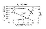
図4はCl2 ガス及びN2 ガスの合計流量に対するN2 ガスの流量比のエッチング依存性を示すグラフである。ここでは左側の縦軸にエッチングレート(エッチング対象層及び下地層)を示し、右側の縦軸に選択比を示している。また図5はN2 ガスの流量比の各代表値、すなわち50%、70%、80%、90%(図5(A)〜図5(D)にそれぞれ対応)の時のエッチング状態を示す電子顕微鏡写真を示す。この時のエッチング条件は、Cl2 ガスとN2 ガスの合計流量を700sccmに一定にし、両ガスの比率を変化させた。またO2 ガスの流量は30sccmに固定した。Here, since the actual evaluation was performed on the quality of the etching shape with respect to the flow rate of each gas and the presence or absence of selectivity with respect to the underlayer, the evaluation results will be described.
Figure 4 is a graph showing the etching dependence of the flow ratio of N2 gas to the total flow rate of Cl2 gas and N2 gas. Here, the left vertical axis represents the etching rate (etching target layer and underlayer), and the right vertical axis represents the selection ratio. Further, FIG. 5 shows the etching state at each representative value of the flow rate ratio of N2 gas, that is, 50%, 70%, 80%, and 90% (corresponding to FIGS. 5A to 5D, respectively). An electron micrograph is shown. The etching conditions at this time were such that the total flow rate of Cl2 gas and N2 gas was fixed at 700 sccm, and the ratio of both gases was changed. The flow rate of O2 gas was fixed at 30 sccm.
図5(A)〜図5(C)は比較的適正なエッチング形状を示しているが、図5(D)はサイドエッチングが発生している。そして、図4のグラフから明らかなように、N2 ガス流量比を増加する程、エッチング対象層のエッチングレートはそれ程低下しないのに対して、下地層のエッチングレートは大幅に低下するので、選択比は向上して好ましい。しかし、N2 ガス流量比が80%を超えて大きくなると、エッチング対象層のエッチングレートが過度に低下するのみならず、グラフには現れていないが、図5(D)に示すようにエッチング対象層にサイドエッチングが発生して好ましくない。またN2 ガス流量比が50%よりも小さい場合には、選択比が小さくなり過ぎてしまって好ましくない。従って、N2 ガス流量比は、50〜80%の範囲内であることが必要であり、特に70〜80%の範囲内においては選択比が実用上十分な値である3.0以上となり、更に好ましいことが確認できた。FIGS. 5A to 5C show a relatively appropriate etching shape, but FIG. 5D shows side etching. As apparent from the graph of FIG. 4, the etching rate of the etching target layer does not decrease so much as the N2 gas flow rate ratio increases, but the etching rate of the underlayer greatly decreases. The ratio is preferably improved. However, when the N2 gas flow rate ratio exceeds 80%, not only does the etching rate of the etching target layer decrease excessively, but it does not appear in the graph, but as shown in FIG. Side etching occurs in the layer, which is not preferable. Moreover, when the N2 gas flow rate ratio is smaller than 50%, the selection ratio becomes too small, which is not preferable. Therefore, the N2 gas flow rate ratio needs to be in the range of 50 to 80%, and particularly in the range of 70 to 80%, the selection ratio is 3.0 or more which is a practically sufficient value, It was further confirmed that it was preferable.
図6はCl2 ガス及びN2 ガスの合計流量に対するO2 ガスの添加量と下地層に対する選択性との関係を示すグラフである。ここでは左側の縦軸にエッチングレート(エッチング対象層及び下地層)を示し、右側の縦軸に選択比を示している。図7はO2 ガスの添加量の各代表値、すなわち2.9%、4.3%、5.7%、8.6%、11.4%の時(図7(A)〜図7(E)にそれぞれ対応)の電子顕微鏡写真を示す。またこの時のプロセス条件は、Cl2 ガスとN2 ガスの流量をそれぞれ200sccm及び500sccmに固定し、O2 ガスの流量のみを変化させた。
図7(A)〜図7(D)は比較的適正なエッチング形状を示しているが、図7(E)は側壁にデポが発生している。そして、図6から明らかなように、O2 ガスの添加量が多くなる程、エッチング対象層のエッチングレートは大きくなるのに対して、下地層のエッチングレートは低下し、従って、選択比は増加している。しかし、O2 ガスの添加量が2.9%よりも少ない場合には、エッチングレートが過度に低下してしまって好ましくない。これに対して、O2 ガスの添加量が8.6%よりも大きくなると、図7(E)に示すように側壁にデポが発生してエッチング形状が劣化してしまって好ましくない。この結果、O2 ガスの添加量が2.9〜8.6%の範囲内では、適正な選択比であり、特に4.3〜5.7%の範囲内では、選択比が3.0以上であり、側壁デポも全く発生せず、更に好ましいことが確認できた。FIG. 6 is a graph showing the relationship between the amount of O2 gas added to the total flow rate of Cl2 gas and N2 gas and the selectivity to the underlying layer. Here, the left vertical axis represents the etching rate (etching target layer and underlayer), and the right vertical axis represents the selection ratio. FIG. 7 shows typical values of the added amount of O2 gas, ie, 2.9%, 4.3%, 5.7%, 8.6%, and 11.4% (FIGS. 7A to 7). Electron micrographs of (corresponding to (E) respectively) are shown. The process conditions at this time were such that the flow rates of Cl2 gas and N2 gas were fixed at 200 sccm and 500 sccm, respectively, and only the flow rate of O2 gas was changed.
7A to 7D show a relatively appropriate etching shape, but FIG. 7E shows a deposit on the side wall. As can be seen from FIG. 6, as the amount of O2 gas added increases, the etching rate of the etching target layer increases, whereas the etching rate of the underlying layer decreases, and the selectivity increases accordingly. is doing. However, when the amount of O2 gas added is less than 2.9%, the etching rate is undesirably lowered. On the other hand, when the amount of O2 gas added is larger than 8.6%, deposits are generated on the side walls as shown in FIG. As a result, when the addition amount of O2 gas is in the range of 2.9 to 8.6%, the selection ratio is appropriate, and particularly in the range of 4.3 to 5.7%, the selection ratio is 3.0. As described above, no side wall deposit was generated, and it was confirmed that it was more preferable.
上記実施例では、塩素含有ガスとしてCl2 ガスを用いたが、これに限定されず、例えばBCl3 等を用いることができる。また上記実施例では、添加ガスとして酸素含有ガスと窒素含有ガスの2種類のガスを用いたが、この2種類のガスに代えて酸化窒素ガスを用いてもよい。この酸化窒素ガスとしては、例えばNOガス、N2 Oガス、NO2 ガス等を用いることができる。In the above embodiment, Cl2 gas is used as the chlorine-containing gas. However, the present invention is not limited to this. For example, BCl3 or the like can be used. Moreover, in the said Example, although two types of gas, oxygen-containing gas and nitrogen-containing gas, was used as additive gas, it may replace with these two types of gas and nitrogen oxide gas may be used. As this nitrogen oxide gas, for example, NO gas, N2 O gas, NO2 gas or the like can be used.
またここでは、被処理体である半導体ウエハSの断面構造としては、下地層4としてポリシリコン層が形成されている場合を例にとって説明したが、これに代えて下地層4がシリコン単結晶よりなる場合にも本発明を適用することができる。また、エッチング対象層6としては、窒化タングステン膜6Aとタングステン膜6Bの積層構造に限定されず、タングステンを含む材料であるならば、どのような膜でもよく、例えば窒化タングステン膜だけの単層、或いはタングステン膜だけの単層の場合にも本発明を適用することができる。
更に、被処理体としては半導体ウエハに限定されず、LCD基板、ガラス基板等にも本発明を適用することができる。Here, the case where the polysilicon layer is formed as the
Furthermore, the object to be processed is not limited to a semiconductor wafer, and the present invention can also be applied to an LCD substrate, a glass substrate, and the like.
4 下地層
6 エッチング対象層
6A 窒化タングステン膜
6B タングステン膜
22 エッチング装置
24 処理容器
26 載置台
44 プラズマ形成手段
46 平面アンテナ部材
60 マイクロ波発生器
64 ガス供給手段
70 シャワーヘッド部
80A Cl2 ガス源
80B O2 ガス源
80C N2 ガス源
90 加熱手段
106 バイアス用高周波電源
108 制御手段
110 記憶媒体
S 半導体ウエハ(被処理体)
DESCRIPTION OF
Claims (3)
Translated fromJapanese前記エッチング時のガスとしてCl2 よりなる塩素含有ガスとO2 よりなる酸素含有ガスとN2 よりなる窒素含有ガスのみとを用いると共に、前記塩素含有ガス及び前記窒素含有ガスの合計流量に対する前記酸素含有ガスの添加量は2.9〜8.6%の範囲内であり、前記塩素含有ガス及び前記窒素含有ガスの合計流量に対する前記窒素含有ガスの流量比は50〜80%の範囲内であるようにしたことを特徴とするエッチング方法。The presence of plasma in a vacuum evacuable processing vessel polysilicondown layer by Li Cheng underlayer relative to the workpiecewhich the laminated structure by Li Cheng etching target layer is formedbetween the tungsten nitride film and a tungsten film In an etching method in which an etching process is performed below,
With using only an oxygen-containing nitrogen-containing gasconsisting of gas andN2consisting ofchlorine-containing gas andO2consisting ofCl2 as gas during the etching, the to the total flow rate of the chlorine-containing gas and the nitrogen-containing gas The addition amount of the oxygen-containing gas is in the range of 2.9 to 8.6%, and the flow rate ratio of the nitrogen-containing gas to the total flow rate of the chlorine-containing gas and the nitrogen-containing gas is in the range of 50 to 80%. An etching method characterized by being provided.
Priority Applications (6)
| Application Number | Priority Date | Filing Date | Title |
|---|---|---|---|
| JP2004344608AJP4701691B2 (en) | 2004-11-29 | 2004-11-29 | Etching method |
| US11/791,718US7842617B2 (en) | 2004-11-29 | 2005-11-18 | Etching method and etching apparatus |
| PCT/JP2005/021256WO2006057202A1 (en) | 2004-11-29 | 2005-11-18 | Etching method and etching apparatus |
| CN200580040949ACN100580887C (en) | 2004-11-29 | 2005-11-18 | Etching method |
| KR1020077014786AKR100910681B1 (en) | 2004-11-29 | 2005-11-18 | Etching method and etching apparatus |
| TW094141915ATWI385721B (en) | 2004-11-29 | 2005-11-29 | Etching method and etching device |
Applications Claiming Priority (1)
| Application Number | Priority Date | Filing Date | Title |
|---|---|---|---|
| JP2004344608AJP4701691B2 (en) | 2004-11-29 | 2004-11-29 | Etching method |
Publications (3)
| Publication Number | Publication Date |
|---|---|
| JP2006156675A JP2006156675A (en) | 2006-06-15 |
| JP2006156675A5 JP2006156675A5 (en) | 2008-02-07 |
| JP4701691B2true JP4701691B2 (en) | 2011-06-15 |
Family
ID=36497939
Family Applications (1)
| Application Number | Title | Priority Date | Filing Date |
|---|---|---|---|
| JP2004344608AExpired - Fee RelatedJP4701691B2 (en) | 2004-11-29 | 2004-11-29 | Etching method |
Country Status (6)
| Country | Link |
|---|---|
| US (1) | US7842617B2 (en) |
| JP (1) | JP4701691B2 (en) |
| KR (1) | KR100910681B1 (en) |
| CN (1) | CN100580887C (en) |
| TW (1) | TWI385721B (en) |
| WO (1) | WO2006057202A1 (en) |
Families Citing this family (51)
| Publication number | Priority date | Publication date | Assignee | Title |
|---|---|---|---|---|
| EP1115147A4 (en)* | 1999-05-26 | 2007-05-02 | Tadahiro Ohmi | PLASMA TREATMENT DEVICE |
| KR101418438B1 (en)* | 2007-07-10 | 2014-07-14 | 삼성전자주식회사 | Plasma generator |
| WO2009084194A1 (en)* | 2007-12-28 | 2009-07-09 | Tokyo Electron Limited | Etching method for metal film and metal oxide film, and manufacturing method for semiconductor device |
| JP2010118549A (en)* | 2008-11-13 | 2010-05-27 | Tokyo Electron Ltd | Plasma etching method and plasma etching device |
| US20110061810A1 (en)* | 2009-09-11 | 2011-03-17 | Applied Materials, Inc. | Apparatus and Methods for Cyclical Oxidation and Etching |
| US20110065276A1 (en)* | 2009-09-11 | 2011-03-17 | Applied Materials, Inc. | Apparatus and Methods for Cyclical Oxidation and Etching |
| US20110061812A1 (en)* | 2009-09-11 | 2011-03-17 | Applied Materials, Inc. | Apparatus and Methods for Cyclical Oxidation and Etching |
| JP2011174540A (en)* | 2010-02-24 | 2011-09-08 | Tokyo Electron Ltd | Ball valve and evacuating device for evacuation |
| US9611544B2 (en) | 2010-04-15 | 2017-04-04 | Novellus Systems, Inc. | Plasma activated conformal dielectric film deposition |
| US9257274B2 (en) | 2010-04-15 | 2016-02-09 | Lam Research Corporation | Gapfill of variable aspect ratio features with a composite PEALD and PECVD method |
| US9373500B2 (en) | 2014-02-21 | 2016-06-21 | Lam Research Corporation | Plasma assisted atomic layer deposition titanium oxide for conformal encapsulation and gapfill applications |
| US9997357B2 (en) | 2010-04-15 | 2018-06-12 | Lam Research Corporation | Capped ALD films for doping fin-shaped channel regions of 3-D IC transistors |
| US8637411B2 (en) | 2010-04-15 | 2014-01-28 | Novellus Systems, Inc. | Plasma activated conformal dielectric film deposition |
| US9892917B2 (en) | 2010-04-15 | 2018-02-13 | Lam Research Corporation | Plasma assisted atomic layer deposition of multi-layer films for patterning applications |
| KR101772723B1 (en)* | 2010-06-28 | 2017-08-29 | 도쿄엘렉트론가부시키가이샤 | Plasma processing method |
| JP5845754B2 (en) | 2010-09-15 | 2016-01-20 | 東京エレクトロン株式会社 | Plasma etching processing method |
| US9685320B2 (en) | 2010-09-23 | 2017-06-20 | Lam Research Corporation | Methods for depositing silicon oxide |
| JP5413342B2 (en)* | 2010-09-27 | 2014-02-12 | 株式会社Sumco | Silicon wafer surface layer etching method and silicon wafer metal contamination analysis method |
| JP5916044B2 (en)* | 2010-09-28 | 2016-05-11 | 東京エレクトロン株式会社 | Plasma processing apparatus and plasma processing method |
| US8562785B2 (en)* | 2011-05-31 | 2013-10-22 | Lam Research Corporation | Gas distribution showerhead for inductively coupled plasma etch reactor |
| US9245717B2 (en) | 2011-05-31 | 2016-01-26 | Lam Research Corporation | Gas distribution system for ceramic showerhead of plasma etch reactor |
| JP5377587B2 (en)* | 2011-07-06 | 2013-12-25 | 東京エレクトロン株式会社 | Antenna, plasma processing apparatus, and plasma processing method |
| US8808562B2 (en)* | 2011-09-12 | 2014-08-19 | Tokyo Electron Limited | Dry metal etching method |
| US8592328B2 (en) | 2012-01-20 | 2013-11-26 | Novellus Systems, Inc. | Method for depositing a chlorine-free conformal sin film |
| JP6538300B2 (en) | 2012-11-08 | 2019-07-03 | ノベラス・システムズ・インコーポレーテッドNovellus Systems Incorporated | Method for depositing a film on a sensitive substrate |
| US9893276B2 (en) | 2013-06-27 | 2018-02-13 | Nec Corporation | Switching element, switching element manufacturing method, semiconductor device, and semiconductor device manufacturing method |
| US9589790B2 (en) | 2014-11-24 | 2017-03-07 | Lam Research Corporation | Method of depositing ammonia free and chlorine free conformal silicon nitride film |
| US9564312B2 (en) | 2014-11-24 | 2017-02-07 | Lam Research Corporation | Selective inhibition in atomic layer deposition of silicon-containing films |
| US9633867B2 (en)* | 2015-01-05 | 2017-04-25 | Lam Research Corporation | Method and apparatus for anisotropic tungsten etching |
| US10566187B2 (en) | 2015-03-20 | 2020-02-18 | Lam Research Corporation | Ultrathin atomic layer deposition film accuracy thickness control |
| US9601693B1 (en) | 2015-09-24 | 2017-03-21 | Lam Research Corporation | Method for encapsulating a chalcogenide material |
| JP6766184B2 (en)* | 2016-06-03 | 2020-10-07 | インテグリス・インコーポレーテッド | Hafnia and zirconia vapor phase etching |
| US9773643B1 (en) | 2016-06-30 | 2017-09-26 | Lam Research Corporation | Apparatus and method for deposition and etch in gap fill |
| US10062563B2 (en) | 2016-07-01 | 2018-08-28 | Lam Research Corporation | Selective atomic layer deposition with post-dose treatment |
| US10629435B2 (en) | 2016-07-29 | 2020-04-21 | Lam Research Corporation | Doped ALD films for semiconductor patterning applications |
| US10074543B2 (en) | 2016-08-31 | 2018-09-11 | Lam Research Corporation | High dry etch rate materials for semiconductor patterning applications |
| US10037884B2 (en) | 2016-08-31 | 2018-07-31 | Lam Research Corporation | Selective atomic layer deposition for gapfill using sacrificial underlayer |
| US9865455B1 (en) | 2016-09-07 | 2018-01-09 | Lam Research Corporation | Nitride film formed by plasma-enhanced and thermal atomic layer deposition process |
| JP6725176B2 (en)* | 2016-10-31 | 2020-07-15 | 株式会社日立ハイテク | Plasma etching method |
| US10454029B2 (en) | 2016-11-11 | 2019-10-22 | Lam Research Corporation | Method for reducing the wet etch rate of a sin film without damaging the underlying substrate |
| US10832908B2 (en) | 2016-11-11 | 2020-11-10 | Lam Research Corporation | Self-aligned multi-patterning process flow with ALD gapfill spacer mask |
| US10134579B2 (en) | 2016-11-14 | 2018-11-20 | Lam Research Corporation | Method for high modulus ALD SiO2 spacer |
| US10373804B2 (en)* | 2017-02-03 | 2019-08-06 | Applied Materials, Inc. | System for tunable workpiece biasing in a plasma reactor |
| US10269559B2 (en) | 2017-09-13 | 2019-04-23 | Lam Research Corporation | Dielectric gapfill of high aspect ratio features utilizing a sacrificial etch cap layer |
| CN112005343B (en) | 2018-03-02 | 2025-05-06 | 朗姆研究公司 | Selective deposition using hydrolysis |
| KR102726216B1 (en) | 2019-05-01 | 2024-11-04 | 램 리써치 코포레이션 | Modulated atomic layer deposition |
| KR102837863B1 (en) | 2019-06-04 | 2025-07-23 | 램 리써치 코포레이션 | Polymeric protective liner for reactive ion etching during patterning |
| JP2022534793A (en) | 2019-06-07 | 2022-08-03 | ラム リサーチ コーポレーション | In situ control of film properties during atomic layer deposition |
| CN114207184A (en) | 2019-08-06 | 2022-03-18 | 朗姆研究公司 | Thermal Atomic Layer Deposition of Silicon-Containing Films |
| CN113643973B (en)* | 2020-04-27 | 2024-11-08 | 中微半导体设备(上海)股份有限公司 | A method and device for low temperature etching |
| CN115735261A (en) | 2020-07-28 | 2023-03-03 | 朗姆研究公司 | Impurity reduction in silicon-containing films |
Family Cites Families (12)
| Publication number | Priority date | Publication date | Assignee | Title |
|---|---|---|---|---|
| JPS6050923A (en)* | 1983-08-31 | 1985-03-22 | Hitachi Ltd | Method of plasma surface treatment and device therefor |
| JPS6265331A (en)* | 1985-09-17 | 1987-03-24 | Hitachi Ltd | Etching method for copper or copper alloy |
| US5880033A (en)* | 1996-06-17 | 1999-03-09 | Applied Materials, Inc. | Method for etching metal silicide with high selectivity to polysilicon |
| JPH11135481A (en) | 1997-10-28 | 1999-05-21 | Yamaha Corp | Etching method |
| US6217704B1 (en)* | 1998-09-22 | 2001-04-17 | Canon Kabushiki Kaisha | Plasma processing apparatus |
| JP2000252259A (en)* | 1999-02-25 | 2000-09-14 | Sony Corp | Dry etching method and manufacture of semiconductor device |
| JP2002025986A (en)* | 2000-07-06 | 2002-01-25 | Matsushita Electric Ind Co Ltd | Dry etching method |
| JP4717295B2 (en)* | 2000-10-04 | 2011-07-06 | 株式会社半導体エネルギー研究所 | Dry etching apparatus and etching method |
| JP4402860B2 (en)* | 2001-03-28 | 2010-01-20 | 忠弘 大見 | Plasma processing equipment |
| JP4147017B2 (en)* | 2001-10-19 | 2008-09-10 | 東京エレクトロン株式会社 | Microwave plasma substrate processing equipment |
| JP2004119781A (en)* | 2002-09-27 | 2004-04-15 | Sharp Corp | Dry etching method |
| JP2004273532A (en)* | 2003-03-05 | 2004-09-30 | Hitachi High-Technologies Corp | Plasma etching method |
- 2004
- 2004-11-29JPJP2004344608Apatent/JP4701691B2/ennot_activeExpired - Fee Related
- 2005
- 2005-11-18WOPCT/JP2005/021256patent/WO2006057202A1/enactiveApplication Filing
- 2005-11-18USUS11/791,718patent/US7842617B2/ennot_activeExpired - Fee Related
- 2005-11-18KRKR1020077014786Apatent/KR100910681B1/ennot_activeExpired - Fee Related
- 2005-11-18CNCN200580040949Apatent/CN100580887C/ennot_activeExpired - Fee Related
- 2005-11-29TWTW094141915Apatent/TWI385721B/ennot_activeIP Right Cessation
Also Published As
| Publication number | Publication date |
|---|---|
| US20080138996A1 (en) | 2008-06-12 |
| CN101069272A (en) | 2007-11-07 |
| WO2006057202A1 (en) | 2006-06-01 |
| TW200636851A (en) | 2006-10-16 |
| TWI385721B (en) | 2013-02-11 |
| JP2006156675A (en) | 2006-06-15 |
| KR20070086761A (en) | 2007-08-27 |
| CN100580887C (en) | 2010-01-13 |
| KR100910681B1 (en) | 2009-08-04 |
| US7842617B2 (en) | 2010-11-30 |
Similar Documents
| Publication | Publication Date | Title |
|---|---|---|
| JP4701691B2 (en) | Etching method | |
| TWI515791B (en) | Plasma etching method and plasma etching device | |
| US7825018B2 (en) | Plasma oxidation method and method for manufacturing semiconductor device | |
| CN100565816C (en) | Engraving method and Etaching device | |
| CN102473634B (en) | Plasma processing device and plasma processing method | |
| JP5138261B2 (en) | Silicon oxide film forming method, plasma processing apparatus, and storage medium | |
| US7811945B2 (en) | Selective plasma processing method | |
| US20100093185A1 (en) | Method for forming silicon oxide film, plasma processing apparatus and storage medium | |
| US7972973B2 (en) | Method for forming silicon oxide film, plasma processing apparatus and storage medium | |
| US11201062B2 (en) | Method and apparatus for processing a substrate | |
| US20090137125A1 (en) | Etching method and etching apparatus | |
| KR20100129311A (en) | A method of manufacturing a silicon nitride film, a method of manufacturing a silicon nitride film laminate, a computer readable storage medium, and a plasma CD device | |
| JP2007165788A (en) | Method for decarbonizing metal film, film forming method, and method for manufacturing semiconductor device | |
| US11264248B2 (en) | Etching method and substrate processing apparatus | |
| TW202043520A (en) | Methods and apparatus for filling a feature disposed in a substrate | |
| JP2009267391A (en) | Process for producing silicon nitride film, process for producing silicon nitride film laminate, computer-readable storage medium, and plasma cvd device | |
| JP2009246210A (en) | Method for forming silicon nitride film, method for manufacturing silicon nitride film laminate, computer-readable storage medium and plasma cvd apparatus |
Legal Events
| Date | Code | Title | Description |
|---|---|---|---|
| A521 | Request for written amendment filed | Free format text:JAPANESE INTERMEDIATE CODE: A523 Effective date:20071107 | |
| A621 | Written request for application examination | Free format text:JAPANESE INTERMEDIATE CODE: A621 Effective date:20071107 | |
| A131 | Notification of reasons for refusal | Free format text:JAPANESE INTERMEDIATE CODE: A131 Effective date:20100921 | |
| A521 | Request for written amendment filed | Free format text:JAPANESE INTERMEDIATE CODE: A523 Effective date:20101111 | |
| A131 | Notification of reasons for refusal | Free format text:JAPANESE INTERMEDIATE CODE: A131 Effective date:20101207 | |
| A521 | Request for written amendment filed | Free format text:JAPANESE INTERMEDIATE CODE: A523 Effective date:20110119 | |
| TRDD | Decision of grant or rejection written | ||
| A01 | Written decision to grant a patent or to grant a registration (utility model) | Free format text:JAPANESE INTERMEDIATE CODE: A01 Effective date:20110208 | |
| A61 | First payment of annual fees (during grant procedure) | Free format text:JAPANESE INTERMEDIATE CODE: A61 Effective date:20110221 | |
| R150 | Certificate of patent or registration of utility model | Ref document number:4701691 Country of ref document:JP Free format text:JAPANESE INTERMEDIATE CODE: R150 | |
| R250 | Receipt of annual fees | Free format text:JAPANESE INTERMEDIATE CODE: R250 | |
| R250 | Receipt of annual fees | Free format text:JAPANESE INTERMEDIATE CODE: R250 | |
| R250 | Receipt of annual fees | Free format text:JAPANESE INTERMEDIATE CODE: R250 | |
| R250 | Receipt of annual fees | Free format text:JAPANESE INTERMEDIATE CODE: R250 | |
| R250 | Receipt of annual fees | Free format text:JAPANESE INTERMEDIATE CODE: R250 | |
| LAPS | Cancellation because of no payment of annual fees |