JP4701565B2 - Light source unit mounting structure - Google Patents
Light source unit mounting structureDownload PDFInfo
- Publication number
- JP4701565B2 JP4701565B2JP2001268477AJP2001268477AJP4701565B2JP 4701565 B2JP4701565 B2JP 4701565B2JP 2001268477 AJP2001268477 AJP 2001268477AJP 2001268477 AJP2001268477 AJP 2001268477AJP 4701565 B2JP4701565 B2JP 4701565B2
- Authority
- JP
- Japan
- Prior art keywords
- light source
- source unit
- sleeve
- mounting structure
- unit mounting
- Prior art date
- Legal status (The legal status is an assumption and is not a legal conclusion. Google has not performed a legal analysis and makes no representation as to the accuracy of the status listed.)
- Expired - Fee Related
Links
Images


Classifications
- H—ELECTRICITY
- H01—ELECTRIC ELEMENTS
- H01L—SEMICONDUCTOR DEVICES NOT COVERED BY CLASS H10
- H01L2224/00—Indexing scheme for arrangements for connecting or disconnecting semiconductor or solid-state bodies and methods related thereto as covered by H01L24/00
- H01L2224/01—Means for bonding being attached to, or being formed on, the surface to be connected, e.g. chip-to-package, die-attach, "first-level" interconnects; Manufacturing methods related thereto
- H01L2224/10—Bump connectors; Manufacturing methods related thereto
- H01L2224/15—Structure, shape, material or disposition of the bump connectors after the connecting process
- H01L2224/16—Structure, shape, material or disposition of the bump connectors after the connecting process of an individual bump connector
- H01L2224/161—Disposition
- H01L2224/16135—Disposition the bump connector connecting between different semiconductor or solid-state bodies, i.e. chip-to-chip
- H01L2224/16145—Disposition the bump connector connecting between different semiconductor or solid-state bodies, i.e. chip-to-chip the bodies being stacked
- H—ELECTRICITY
- H01—ELECTRIC ELEMENTS
- H01L—SEMICONDUCTOR DEVICES NOT COVERED BY CLASS H10
- H01L2224/00—Indexing scheme for arrangements for connecting or disconnecting semiconductor or solid-state bodies and methods related thereto as covered by H01L24/00
- H01L2224/01—Means for bonding being attached to, or being formed on, the surface to be connected, e.g. chip-to-package, die-attach, "first-level" interconnects; Manufacturing methods related thereto
- H01L2224/26—Layer connectors, e.g. plate connectors, solder or adhesive layers; Manufacturing methods related thereto
- H01L2224/31—Structure, shape, material or disposition of the layer connectors after the connecting process
- H01L2224/32—Structure, shape, material or disposition of the layer connectors after the connecting process of an individual layer connector
- H01L2224/321—Disposition
- H01L2224/32151—Disposition the layer connector connecting between a semiconductor or solid-state body and an item not being a semiconductor or solid-state body, e.g. chip-to-substrate, chip-to-passive
- H01L2224/32221—Disposition the layer connector connecting between a semiconductor or solid-state body and an item not being a semiconductor or solid-state body, e.g. chip-to-substrate, chip-to-passive the body and the item being stacked
- H01L2224/32245—Disposition the layer connector connecting between a semiconductor or solid-state body and an item not being a semiconductor or solid-state body, e.g. chip-to-substrate, chip-to-passive the body and the item being stacked the item being metallic
- H01L2224/32257—Disposition the layer connector connecting between a semiconductor or solid-state body and an item not being a semiconductor or solid-state body, e.g. chip-to-substrate, chip-to-passive the body and the item being stacked the item being metallic the layer connector connecting to a bonding area disposed in a recess of the surface of the item
- H—ELECTRICITY
- H01—ELECTRIC ELEMENTS
- H01L—SEMICONDUCTOR DEVICES NOT COVERED BY CLASS H10
- H01L2224/00—Indexing scheme for arrangements for connecting or disconnecting semiconductor or solid-state bodies and methods related thereto as covered by H01L24/00
- H01L2224/01—Means for bonding being attached to, or being formed on, the surface to be connected, e.g. chip-to-package, die-attach, "first-level" interconnects; Manufacturing methods related thereto
- H01L2224/42—Wire connectors; Manufacturing methods related thereto
- H01L2224/47—Structure, shape, material or disposition of the wire connectors after the connecting process
- H01L2224/48—Structure, shape, material or disposition of the wire connectors after the connecting process of an individual wire connector
- H01L2224/481—Disposition
- H01L2224/48151—Connecting between a semiconductor or solid-state body and an item not being a semiconductor or solid-state body, e.g. chip-to-substrate, chip-to-passive
- H01L2224/48221—Connecting between a semiconductor or solid-state body and an item not being a semiconductor or solid-state body, e.g. chip-to-substrate, chip-to-passive the body and the item being stacked
- H01L2224/48245—Connecting between a semiconductor or solid-state body and an item not being a semiconductor or solid-state body, e.g. chip-to-substrate, chip-to-passive the body and the item being stacked the item being metallic
- H01L2224/48247—Connecting between a semiconductor or solid-state body and an item not being a semiconductor or solid-state body, e.g. chip-to-substrate, chip-to-passive the body and the item being stacked the item being metallic connecting the wire to a bond pad of the item
Landscapes
- Arrangement Of Elements, Cooling, Sealing, Or The Like Of Lighting Devices (AREA)
- Led Device Packages (AREA)
- Led Devices (AREA)
Description
Translated fromJapanese【0001】
【発明の属する技術分野】
本発明は、LEDを利用した半導体発光による照明装置に係り、特に放熱性をよくし大電流の印加を可能として高輝度の発光が得られるようにした光源ユニットの装着構造に関する。
【0002】
【従来の技術】
従来から発光ダイオード(LED)を利用したさまざまな半導体発光装置が開発されている。この半導体発光装置の中で最も典型的なものは砲弾型のランプ状としたものと表面実装用のチップ型としたものであり、図4にランプ状の半導体発光装置の従来例を示す。
【0003】
図4において、二股状のリードフレーム51の一方のリード51aの上端にマウント部51bを形成し、このマウント部51bの上にサブマウント素子52を介してフリップチップ型の半導体発光素子53が導通接続されている。サブマウント素子52はたとえば静電気保護素子であり、下面にマウント部51bに導通させるための電極52aを形成し、上面の電極にはワイヤ54をリード51cとの間にボンディングしている。そして、ワイヤ54を含めてリードフレーム51の上端はエポキシの樹脂パッケージ55によって封止されている。
【0004】
リードフレーム51を介して半導体発光素子53に通電すると、半導体発光素子53の基板に積層した化合物半導体の活性層から発光する。この通電の際には、半導体発光素子53が発熱する。
【0005】
【発明が解決しようとする課題】
ところが、半導体発光素子53からの発熱は樹脂パッケージ55やリードフレーム51側に熱伝達されるが、樹脂パッケージ55の放熱性は低く、半導体発光素子53を搭載しているリード51aへの熱伝達量も少ない。特に、半導体発光素子53がサファイアを基板としてGaN系化合物半導体を積層した青色発光のものでは、サファイアの基板の熱伝導率が低いので放熱性は格段に低い。また、サブマウント素子52にSiを用いることにより、これを経由した熱の流れはよくなるが、リードフレーム51が細いので結果的に放熱性は悪くなる。
【0006】
このように従来の半導体発光装置では、半導体発光素子53から発生する熱の放熱性が低いので、現状では20mA程度の電流しか印加できない。これよりも大きな電流を印加すると半導体発光素子53の温度が上昇し、流す電流に比例して発光輝度が増加せず飽和してしまうし、特性が劣化して発光輝度が低下してしまう。したがって、半導体発光素子53には小さな電流しか印加できず、その発光輝度にも限界がある。このため、たとえば植物栽培用の光源や照明用の光源として利用しようとする場合では、多数の半導体発光装置を備える必要があり、光源装置が複雑になるとともにコストも高くなるという問題がある。また、半導体発光素子の発熱をリードフレームに移動できたとしても、リードフレームから電源側に放熱する必要がある。
【0007】
そこで、本発明は、半導体発光素子の放熱を促し大電流印加による高輝度化が可能な光源ユニットの装着構造を提供することを目的とする。
【0008】
【課題を解決するための手段】
本発明は、内側に放熱ブロックを、外側にスリーブを熱伝達可能に設けた光源ユニットの装着構造であって、嵌入する放熱ブロックを半径方向内側に付勢して固定する付勢部材を有しているので、放熱ブロックの軸方向位置によって付勢力が変わらないので、放熱ブロックを壁部に安定して保持し、熱の流れがスムーズになる。
【0009】
この発明によれば、半導体発光素子の放熱を促し大電流印加による高輝度化が可能な光源ユニットの装着構造が得られる。
【0010】
【発明の実施の形態】
請求項1記載の発明は、内側に第1の電極になる放熱ブロックを設け、前記放熱ブロックの先部外側に絶縁膜を挟んで第2の電極になるスリーブを熱伝達可能に設け、取り付けられた半導体発光素子に通電可能な光源ユニットの装着構造であって、金属製の壁部に絶縁体を介して設けられ、前記スリーブが嵌入可能な取付孔が形成された取付板と、前記壁部に形成され前記取付孔に連通する取付凹部と、前記取付凹部の周壁に設けられ、嵌入する前記放熱ブロックを半径方向内側に付勢して固定する付勢部材と、前記取付孔の周壁に設けられ、嵌入する前記スリーブを固定する固定部とを有することを特徴とする光源ユニットの装着構造なので、付勢部材が放熱ブロックを側方から押圧することになり、付勢部材の軸方向位置によらず均一な力で放熱ブロックを保持することができる。
【0011】
請求項2記載の発明は、前記スリーブの外周には雄ねじが形成され、前記固定部は前記雄ねじに螺合する雌ねじであることを特徴とする請求項1記載の光源ユニットの装着構造なので、光源ユニットの抜け落ちを防止して、確実に固定することができる。
【0012】
請求項3記載の発明は、前記付勢部材は、屈曲した中間部が先側に突出する板ばねであって、複数設けられていることを特徴とする請求項1又は2記載の光源ユニットの装着構造であり、光源ユニットを先側から嵌入させようとすると、放熱ブロックの先端が板ばねに当接、摺動しながら徐々に大きな力を受けるので、取付時に必要な力の変化を小さくして容易に取り付けることができる。
【0013】
請求項4記載の発明は、前記固定部は嵌入する前記スリーブを半径方向内側に付勢して固定する先部付勢部材であることを特徴とする請求項1記載の光源ユニットの装着構造であり、光源ユニットの軸方向の2カ所を半径方向に固定して容易に着脱することができる。
【0014】
(第1実施形態)
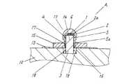
図1は本発明の第1の実施の形態に係る光源ユニットの装着構造の縦断面図である。まず、光源ユニット11について説明する。
【0015】
光源ユニット11は、GaN系化合物半導体をサファイア基板に積層した青色発光の4台の半導体発光素子1の表面をたとえば(Y,Gd)3(Al,Ga)5O12:Ce等の蛍光物質を含む樹脂パッケージで封止した光源を備えたものである。このように青色発光の半導体発光素子1を蛍光物質を含む樹脂パッケージで封止することにより、半導体発光素子1からの光が波長変換されて白色発光として取り出される。
【0016】
4台の半導体発光素子1は静電気保護用のツェナーダイオードなどを利用したサブマウント素子2にそれぞれ導通搭載されている。このサブマウント素子2は熱伝導のよいSiから成り、図示のように放熱ブロック3の上端にAgペーストを介して導通搭載されている。この放熱ブロック3はAlやAgやCuまたはこれらの金属を少なくとも1つ含む合金等のように熱伝導率の高い金属を素材としたもので、下端部を除く外周には絶縁膜4を介して円筒状の金属のスリーブ5を放熱ブロック3に対して熱伝達可能に外挿している。このスリーブ5は外周に雄ねじ5aを形成したもので、各サブマウント素子2との間をワイヤ2aによってボンディングしている。なお、放熱ブロック3は半導体発光素子1のp側電極と導通する第1の電極になり、スリーブ5は半導体発光素子1のn側電極と導通する第2の電極になる。
【0017】
また、放熱ブロック3及びスリーブ5の上端には、半導体発光素子1及びワイヤ2aを含んで封止するエポキシの樹脂パッケージ6が一体化されている。
【0018】
次に光源ユニットの装着構造Aについて説明する。
【0019】
光源ユニット11は金属製の壁部12に取り付けられる。壁部12は導電性を有し、少なくとも一部(例えば上部)に平面を備え、平面には放熱ブロック3より外径が大きい取付凹部16が形成されている。
【0020】
壁部12の上部には、取付凹部16に重合する孔部を備えた絶縁体13が設けられ、絶縁体13の上部には、取付凹部16に連通する取付孔14を備え、導電性を有する取付板15が設けられている。取付孔14の周壁には、スリーブ5の雄ねじ5aに螺合する固定部の一例である雌ねじ17が形成されている。
【0021】
取付凹部16の周壁の対向する2箇所以上には、付勢部材の一例である板ばね18が設けられている。それぞれの板ばね18は、屈曲した中間部が先側に突出する逆V字状又は逆U字状に形成され、嵌入する放熱ブロック3を半径方向内側に付勢して固定することができる。
【0022】
光源ユニット11を壁部12に取り付ける時には、まず、放熱ブロック3を取付孔14に挿通させ、取付凹部16に少し嵌入させる。次いで、スリーブ5の雄ねじ5aを取付孔14の雌ねじ17に螺合させる。このとき、放熱ブロック3は、回転しながら取付凹部16の底部に向かって徐々に移動し、当接する板ばね18から半径方向内側に向かって付勢される。このようにして取付を行うことによって、壁部12は、板ばね18を介して放熱ブロック3に通電可能に接続し、取付板15は、スリーブ5に通電可能に接続される。
【0023】
板ばね18は放熱ブロック3を半径方向内側に付勢するので、放熱ブロック3が所定位置より取付凹部16の底側に移動しすぎても、塑性変形することがなく、付勢力を一定にして通電状態を安定的に保持すると共に板ばねの寿命を長くすることができる。また、放熱ブロック3を取付凹部16の底部に当接させることができるので、放熱ブロック3から壁部12への放熱を効率よく行うことができる。
【0024】
(第2実施形態)
図2は本発明の第2の実施の形態に係る光源ユニットの装着構造の縦断面図である。装着構造Bは、前述した装着構造Aで用いたねじ結合の代わりに付勢手段による結合方式を用いたもので、その他の同一部材については同一番号を付して説明は省略する。
【0025】
光源ユニット19は、スリーブ5の雄ねじ5aを省略した円筒形のスリーブ20を有している。また、取付板21の取付孔22には雌ねじ17が形成されておらず、スリーブ20の外径より大きな周壁には、板ばね18と同形状の先部付勢部材の一例である板ばね23が設けられている。
【0026】
光源ユニット19を壁部12に取り付ける時には、まず、放熱ブロック3を取付孔22に挿通させ、取付凹部16に少し嵌入させる。このとき、放熱ブロック3は、板ばね18に当接し、スリーブ20は板ばね23に当接する。次に、光源ユニット19を取付凹部16の底部に向けて押圧すると、放熱ブロック3及びスリーブ20は、当接する板ばね18,23から半径方向内側に向かって付勢される。
【0027】
このようにして取付を行うことによって、壁部12は、板ばね18を介して放熱ブロック3に通電可能に接続し、取付板21は、板ばね23を介してスリーブ20に通電可能に接続される。光源ユニット19を回転させずに軸方向に移動することができるので、放熱ブロック及びスリーブの外形を断面円形に限らず任意の形状に形成することができ、例えば、正方形や六角形に形成することができ、また、外周に突起部等を設けて取付の向きを規制することもできる。また、取付凹部16及び取付孔22の周壁には、放熱ブロック3及びスリーブ5の半径方向への位置ずれを防止する板状突起を設けることも可能である。さらに絶縁体24を硬質の板状部材で形成し、取付凹部16及び取付孔22に連通する貫通孔の大きさを、放熱ブロック3を位置決めしながら嵌入可能な大きさに形成することも可能である。
【0028】
(第3実施形態)
図3は本発明の第3の実施の形態に係る光源ユニットの装着構造の縦断面図である。装着構造Cは、前述した装着構造Bの放熱ブロックと壁部の固定に用いた付勢手段の代わりにねじ結合を用いたもので、その他の同一部材については同一番号を付して説明は省略する。
【0029】
光源ユニット29の放熱ブロック25の基部には雄ねじ26が形成され、壁部27には雄ねじ26に螺合する雌ねじ28が形成されている。
【0030】
かかる構成によって、放熱ブロック25と壁部27の接触面積が広くなり、放熱がさらに大きくなる。
【0031】
【発明の効果】
本発明では、取付凹部の周壁に設けられ、嵌入する前記放熱ブロックを半径方向内側に付勢して固定する付勢部材を有しているので、付勢部材が放熱ブロックを側方から押圧することになり、付勢部材の軸方向位置によらず均一な力で放熱ブロックを保持することができ、また、付勢部材の大きな変形を防止して装置寿命を長くすることができる。
【0032】
前記取付凹部の底部に放熱ブロックを当接させることにより、放熱効率を向上させることができる。
【0033】
また、スリーブの外周に雄ねじを形成し、固定部を雌ねじにすることにより、光源ユニットの抜け落ちを防止し確実に固定することができる。
【0034】
前記付勢部材を板ばねで構成することにより構造を簡単にし、取付時に必要な力の変化を小さくして容易に取り付けることができる。
【0035】
前記固定部を先部付勢部材にして、光源ユニットの軸方向の2カ所を半径方向に固定することにより、着脱を容易にすることができる。
【図面の簡単な説明】
【図1】本発明の第1実施の形態における光源ユニットの装着構造の縦断面図
【図2】本発明の第2実施の形態における光源ユニットの装着構造の縦断面図
【図3】本発明の第3実施の形態における光源ユニットの装着構造の縦断面図
【図4】従来の半導体発光装置の縦断面図
【符号の説明】
1 半導体発光素子
2 サブマウント素子
2a ワイヤ
3 放熱ブロック
4 絶縁膜
5 スリーブ
5a 雄ねじ
6 樹脂パッケージ
11 光源ユニット
12 壁部
13 絶縁体
14 取付孔
15 取付板
16 取付凹部
17 雌ねじ(固定部)
18 板ばね(先部付勢部材)
19 光源ユニット
20 スリーブ
21 取付板
22 取付孔
23 板ばね(先部付勢部材)
24 絶縁体
25 放熱ブロック
26 雄ねじ
27 壁部
28 雌ねじ
29 光源ユニット
A 装着構造
B 装着構造
C 装着構造[0001]
BACKGROUND OF THE INVENTION
The present invention relates to a lighting device using semiconductor light emission using LEDs, and more particularly to a light source unit mounting structure that improves heat dissipation and enables application of a large current to obtain high luminance light emission.
[0002]
[Prior art]
Conventionally, various semiconductor light emitting devices using light emitting diodes (LEDs) have been developed. The most typical of these semiconductor light emitting devices are a shell type lamp type and a surface mount chip type. FIG. 4 shows a conventional example of a lamp type semiconductor light emitting device.
[0003]
In FIG. 4, a
[0004]
When the semiconductor
[0005]
[Problems to be solved by the invention]
However, the heat generated from the semiconductor
[0006]
As described above, in the conventional semiconductor light emitting device, since the heat radiation of the heat generated from the semiconductor
[0007]
SUMMARY OF THE INVENTION Accordingly, an object of the present invention is to provide a light source unit mounting structure that promotes heat dissipation of a semiconductor light emitting element and can increase brightness by applying a large current.
[0008]
[Means for Solving the Problems]
The present invention is a mounting structure of a light source unit in which a heat dissipation block is provided on the inner side and a sleeve is provided on the outer side so that heat can be transferred, and includes a biasing member that biases and fixes the heat dissipation block to be inserted inward in the radial direction. Therefore, since the urging force does not change depending on the axial position of the heat dissipation block, the heat dissipation block is stably held on the wall portion, and the heat flow becomes smooth.
[0009]
According to the present invention, it is possible to obtain a light source unit mounting structure that promotes heat dissipation of a semiconductor light emitting element and can increase brightness by applying a large current.
[0010]
DETAILED DESCRIPTION OF THE INVENTION
According to the first aspect of the present invention, a heat radiation block serving as the first electrode is provided on the inner side, and a sleeve serving as the second electrode is provided on the outer side of the front portion of the heat radiation block with an insulating film interposed therebetween so that heat can be transferred. A mounting structure of a light source unit capable of energizing the semiconductor light emitting element, the mounting plate being provided through a metal wall portion with an insulator, and having a mounting hole into which the sleeve can be fitted, and the wall portion Provided on the peripheral wall of the mounting recess, and provided on the peripheral wall of the mounting recess, and provided on the peripheral wall of the mounting hole. The light source unit mounting structure has a fixing portion for fixing the sleeve to be inserted, and the biasing member presses the heat radiating block from the side, so that the biasing member is positioned at the axial position. Uniform In can hold the heat sink block.
[0011]
According to a second aspect of the present invention, there is provided a light source unit mounting structure according to the first aspect, wherein a male screw is formed on an outer periphery of the sleeve, and the fixing portion is a female screw screwed into the male screw. It is possible to prevent the unit from falling off and fix it securely.
[0012]
According to a third aspect of the present invention, in the light source unit according to the first or second aspect, the urging member is a leaf spring having a bent intermediate portion protruding forward, and a plurality of the biasing members are provided. With the mounting structure, if the light source unit is inserted from the front side, the tip of the radiating block abuts against the leaf spring and gradually receives a large force while sliding, reducing the change in force required during installation. Can be easily installed.
[0013]
According to a fourth aspect of the present invention, in the light source unit mounting structure according to the first aspect, the fixing portion is a tip urging member that urges and fixes the sleeve to be fitted radially inward. Yes, it is possible to attach and detach easily by fixing two axial positions of the light source unit in the radial direction.
[0014]
(First embodiment)
FIG. 1 is a longitudinal sectional view of a light source unit mounting structure according to a first embodiment of the present invention. First, the
[0015]
The
[0016]
The four semiconductor light emitting elements 1 are each conductively mounted on a submount element 2 using a Zener diode for electrostatic protection or the like. The submount element 2 is made of Si having good heat conduction, and is electrically mounted on the upper end of the
[0017]
Also, an
[0018]
Next, the light source unit mounting structure A will be described.
[0019]
The
[0020]
An
[0021]
Leaf springs 18, which are examples of biasing members, are provided at two or more locations on the peripheral wall of the mounting
[0022]
When attaching the
[0023]
Since the
[0024]
(Second Embodiment)
FIG. 2 is a longitudinal sectional view of a light source unit mounting structure according to the second embodiment of the present invention. The mounting structure B uses a coupling method using biasing means instead of the screw coupling used in the above-described mounting structure A, and other identical members are denoted by the same reference numerals and description thereof is omitted.
[0025]
The
[0026]
When attaching the
[0027]
By performing attachment in this way, the
[0028]
(Third embodiment)
FIG. 3 is a longitudinal sectional view of a light source unit mounting structure according to the third embodiment of the present invention. The mounting structure C uses screw coupling instead of the urging means used to fix the heat dissipating block and the wall portion of the mounting structure B described above, and other identical members are denoted by the same reference numerals and description thereof is omitted. To do.
[0029]
A
[0030]
With this configuration, the contact area between the
[0031]
【The invention's effect】
In the present invention, the biasing member is provided on the peripheral wall of the mounting recess, and biases the heat dissipating block to be fitted inward in the radial direction so that the heat dissipating block is pressed from the side. Thus, the heat radiation block can be held with a uniform force regardless of the axial position of the biasing member, and the device life can be extended by preventing a large deformation of the biasing member.
[0032]
Heat dissipation efficiency can be improved by bringing the heat dissipation block into contact with the bottom of the mounting recess.
[0033]
Further, by forming a male screw on the outer periphery of the sleeve and using a female screw as the fixing portion, the light source unit can be prevented from coming off and fixed securely.
[0034]
By constituting the urging member with a leaf spring, the structure can be simplified, and the change in force required at the time of attachment can be reduced and the attachment can be made easily.
[0035]
By using the fixing portion as a tip urging member and fixing two axial positions of the light source unit in the radial direction, the attachment and detachment can be facilitated.
[Brief description of the drawings]
FIG. 1 is a longitudinal sectional view of a light source unit mounting structure according to a first embodiment of the present invention. FIG. 2 is a longitudinal sectional view of a light source unit mounting structure according to a second embodiment of the present invention. FIG. 4 is a longitudinal sectional view of a light source unit mounting structure according to a third embodiment of the present invention. FIG. 4 is a longitudinal sectional view of a conventional semiconductor light emitting device.
DESCRIPTION OF SYMBOLS 1 Semiconductor light-emitting device 2 Submount
18 Leaf spring (tip biasing member)
19
24
Claims (4)
Translated fromJapanese金属製の壁部に絶縁体を介して設けられ、前記スリーブが嵌入可能な取付孔が形成された取付板と、
前記壁部に形成され前記取付孔に連通する取付凹部と、
前記取付凹部の周壁に設けられ、嵌入する前記放熱ブロックを半径方向内側に付勢して固定する付勢部材と、
前記取付孔の周壁に設けられ、嵌入する前記スリーブを固定する固定部とを有することを特徴とする光源ユニットの装着構造。A heat dissipating block serving as a first electrode is provided on the inner side, and a sleeve serving as a second electrode is provided outside the front portion of the heat dissipating block with an insulating film interposed therebetween so as to be able to transfer heat so that the attached semiconductor light emitting element can be energized A light source unit mounting structure,
A mounting plate provided with an insulator on a wall made of metal and having a mounting hole into which the sleeve can be fitted; and
A mounting recess formed in the wall and communicating with the mounting hole;
An urging member provided on the peripheral wall of the mounting recess and urging and fixing the heat dissipating block to be inserted radially inward;
A light source unit mounting structure, comprising: a fixing portion that is provided on a peripheral wall of the mounting hole and fixes the sleeve to be fitted.
Priority Applications (1)
| Application Number | Priority Date | Filing Date | Title |
|---|---|---|---|
| JP2001268477AJP4701565B2 (en) | 2001-09-05 | 2001-09-05 | Light source unit mounting structure |
Applications Claiming Priority (1)
| Application Number | Priority Date | Filing Date | Title |
|---|---|---|---|
| JP2001268477AJP4701565B2 (en) | 2001-09-05 | 2001-09-05 | Light source unit mounting structure |
Publications (2)
| Publication Number | Publication Date |
|---|---|
| JP2003078174A JP2003078174A (en) | 2003-03-14 |
| JP4701565B2true JP4701565B2 (en) | 2011-06-15 |
Family
ID=19094453
Family Applications (1)
| Application Number | Title | Priority Date | Filing Date |
|---|---|---|---|
| JP2001268477AExpired - Fee RelatedJP4701565B2 (en) | 2001-09-05 | 2001-09-05 | Light source unit mounting structure |
Country Status (1)
| Country | Link |
|---|---|
| JP (1) | JP4701565B2 (en) |
Families Citing this family (5)
| Publication number | Priority date | Publication date | Assignee | Title |
|---|---|---|---|---|
| JP2005136224A (en)* | 2003-10-30 | 2005-05-26 | Asahi Kasei Electronics Co Ltd | Light emitting diode lighting module |
| WO2005091390A1 (en)* | 2004-03-18 | 2005-09-29 | Showa Denko K.K. | Group iii nitride semiconductor light-emitting device and producing method thereof |
| JP2006032804A (en)* | 2004-07-20 | 2006-02-02 | Koha Co Ltd | Light emitting device and its manufacturing method |
| EA013884B1 (en)* | 2006-10-10 | 2010-08-30 | Необульб Текнолоджиз Инк. | A semiconductor light-emitting module with heat isolation |
| CN102943966B (en)* | 2007-12-13 | 2015-02-11 | 皇家飞利浦电子股份有限公司 | Light emitting diode disposed on heat dissipating device |
Family Cites Families (3)
| Publication number | Priority date | Publication date | Assignee | Title |
|---|---|---|---|---|
| GB1295306A (en)* | 1969-04-23 | 1972-11-08 | ||
| FR2574616B1 (en)* | 1984-12-07 | 1987-01-23 | Radiotechnique Compelec | MATRIX OF ELECTRO-LUMINESCENT ELEMENT AND MANUFACTURING METHOD THEREOF |
| US6492725B1 (en)* | 2000-02-04 | 2002-12-10 | Lumileds Lighting, U.S., Llc | Concentrically leaded power semiconductor device package |
- 2001
- 2001-09-05JPJP2001268477Apatent/JP4701565B2/ennot_activeExpired - Fee Related
Also Published As
| Publication number | Publication date |
|---|---|
| JP2003078174A (en) | 2003-03-14 |
Similar Documents
| Publication | Publication Date | Title |
|---|---|---|
| CN102472482B (en) | Solid state lighting device with improved heat sink | |
| CN100452448C (en) | Light emitting element and light emitting device with the light emitting element and method for manufacturing the light emitting element | |
| US7795628B2 (en) | LED assembly with separated thermal and electrical structures thereof | |
| CN100468795C (en) | Semiconductor light-emitting device integrating heat conduction/radiation module | |
| US7675086B2 (en) | LED assembly with high heat dissipating capability | |
| JP5516987B2 (en) | Light emitting device and lighting apparatus | |
| CN103325778B (en) | Light-emitting device and ligthing paraphernalia | |
| JP2008523578A (en) | Semiconductor light emitting device, light emitting module, and lighting device | |
| US20150369461A1 (en) | Illumination light source and illumination device | |
| JP4821343B2 (en) | Submount substrate and light emitting device including the same | |
| US8535959B2 (en) | Method for producing large lighting with power LED | |
| JP5849238B2 (en) | Lamp and lighting device | |
| JP5677806B2 (en) | LED bulb | |
| JP2002223007A (en) | Light source unit and semiconductor light emitting lighting device using the same | |
| WO2011158396A1 (en) | Illumination device | |
| KR101018119B1 (en) | LED Package | |
| JP4816394B2 (en) | Spotlight | |
| JP4701565B2 (en) | Light source unit mounting structure | |
| TW506145B (en) | High Luminescence LED having transparent substrate flip-chip type LED die | |
| TWI273858B (en) | Light-emitting diode cluster lamp | |
| JP6519163B2 (en) | Light source device, vehicular lamp provided with the light source device, and method of manufacturing the light source device | |
| KR20140122474A (en) | Led lamp assembly | |
| JP2006344717A (en) | Light-emitting device and its manufacturing method | |
| JP4048750B2 (en) | Semiconductor light-emitting lighting device for plant cultivation | |
| JP2003288806A (en) | Lighting equipment |
Legal Events
| Date | Code | Title | Description |
|---|---|---|---|
| A621 | Written request for application examination | Free format text:JAPANESE INTERMEDIATE CODE: A621 Effective date:20080905 | |
| RD01 | Notification of change of attorney | Free format text:JAPANESE INTERMEDIATE CODE: A7421 Effective date:20081015 | |
| RD01 | Notification of change of attorney | Free format text:JAPANESE INTERMEDIATE CODE: A7421 Effective date:20091119 | |
| A977 | Report on retrieval | Free format text:JAPANESE INTERMEDIATE CODE: A971007 Effective date:20110201 | |
| A01 | Written decision to grant a patent or to grant a registration (utility model) | Free format text:JAPANESE INTERMEDIATE CODE: A01 Effective date:20110208 | |
| A61 | First payment of annual fees (during grant procedure) | Free format text:JAPANESE INTERMEDIATE CODE: A61 Effective date:20110221 | |
| LAPS | Cancellation because of no payment of annual fees |