JP4688983B2 - Inductively coupled HDP-CVD reactor - Google Patents
Inductively coupled HDP-CVD reactorDownload PDFInfo
- Publication number
- JP4688983B2 JP4688983B2JP22293297AJP22293297AJP4688983B2JP 4688983 B2JP4688983 B2JP 4688983B2JP 22293297 AJP22293297 AJP 22293297AJP 22293297 AJP22293297 AJP 22293297AJP 4688983 B2JP4688983 B2JP 4688983B2
- Authority
- JP
- Japan
- Prior art keywords
- gas
- chamber
- coil
- disposed
- source
- Prior art date
- Legal status (The legal status is an assumption and is not a legal conclusion. Google has not performed a legal analysis and makes no representation as to the accuracy of the status listed.)
- Expired - Fee Related
Links
Images


Classifications
- H—ELECTRICITY
- H01—ELECTRIC ELEMENTS
- H01L—SEMICONDUCTOR DEVICES NOT COVERED BY CLASS H10
- H01L21/00—Processes or apparatus adapted for the manufacture or treatment of semiconductor or solid state devices or of parts thereof
- H01L21/02—Manufacture or treatment of semiconductor devices or of parts thereof
- H01L21/04—Manufacture or treatment of semiconductor devices or of parts thereof the devices having potential barriers, e.g. a PN junction, depletion layer or carrier concentration layer
- H01L21/18—Manufacture or treatment of semiconductor devices or of parts thereof the devices having potential barriers, e.g. a PN junction, depletion layer or carrier concentration layer the devices having semiconductor bodies comprising elements of Group IV of the Periodic Table or AIIIBV compounds with or without impurities, e.g. doping materials
- H01L21/20—Deposition of semiconductor materials on a substrate, e.g. epitaxial growth solid phase epitaxy
- H—ELECTRICITY
- H01—ELECTRIC ELEMENTS
- H01J—ELECTRIC DISCHARGE TUBES OR DISCHARGE LAMPS
- H01J37/00—Discharge tubes with provision for introducing objects or material to be exposed to the discharge, e.g. for the purpose of examination or processing thereof
- H01J37/32—Gas-filled discharge tubes
- H01J37/32431—Constructional details of the reactor
- H01J37/3244—Gas supply means
- H01J37/32449—Gas control, e.g. control of the gas flow
- C—CHEMISTRY; METALLURGY
- C23—COATING METALLIC MATERIAL; COATING MATERIAL WITH METALLIC MATERIAL; CHEMICAL SURFACE TREATMENT; DIFFUSION TREATMENT OF METALLIC MATERIAL; COATING BY VACUUM EVAPORATION, BY SPUTTERING, BY ION IMPLANTATION OR BY CHEMICAL VAPOUR DEPOSITION, IN GENERAL; INHIBITING CORROSION OF METALLIC MATERIAL OR INCRUSTATION IN GENERAL
- C23C—COATING METALLIC MATERIAL; COATING MATERIAL WITH METALLIC MATERIAL; SURFACE TREATMENT OF METALLIC MATERIAL BY DIFFUSION INTO THE SURFACE, BY CHEMICAL CONVERSION OR SUBSTITUTION; COATING BY VACUUM EVAPORATION, BY SPUTTERING, BY ION IMPLANTATION OR BY CHEMICAL VAPOUR DEPOSITION, IN GENERAL
- C23C16/00—Chemical coating by decomposition of gaseous compounds, without leaving reaction products of surface material in the coating, i.e. chemical vapour deposition [CVD] processes
- C23C16/44—Chemical coating by decomposition of gaseous compounds, without leaving reaction products of surface material in the coating, i.e. chemical vapour deposition [CVD] processes characterised by the method of coating
- C23C16/50—Chemical coating by decomposition of gaseous compounds, without leaving reaction products of surface material in the coating, i.e. chemical vapour deposition [CVD] processes characterised by the method of coating using electric discharges
- C23C16/505—Chemical coating by decomposition of gaseous compounds, without leaving reaction products of surface material in the coating, i.e. chemical vapour deposition [CVD] processes characterised by the method of coating using electric discharges using radio frequency discharges
- C23C16/507—Chemical coating by decomposition of gaseous compounds, without leaving reaction products of surface material in the coating, i.e. chemical vapour deposition [CVD] processes characterised by the method of coating using electric discharges using radio frequency discharges using external electrodes, e.g. in tunnel type reactors
- H—ELECTRICITY
- H01—ELECTRIC ELEMENTS
- H01J—ELECTRIC DISCHARGE TUBES OR DISCHARGE LAMPS
- H01J37/00—Discharge tubes with provision for introducing objects or material to be exposed to the discharge, e.g. for the purpose of examination or processing thereof
- H01J37/32—Gas-filled discharge tubes
- H01J37/32009—Arrangements for generation of plasma specially adapted for examination or treatment of objects, e.g. plasma sources
- H01J37/32082—Radio frequency generated discharge
- H01J37/321—Radio frequency generated discharge the radio frequency energy being inductively coupled to the plasma
- H—ELECTRICITY
- H01—ELECTRIC ELEMENTS
- H01J—ELECTRIC DISCHARGE TUBES OR DISCHARGE LAMPS
- H01J37/00—Discharge tubes with provision for introducing objects or material to be exposed to the discharge, e.g. for the purpose of examination or processing thereof
- H01J37/32—Gas-filled discharge tubes
- H01J37/32431—Constructional details of the reactor
- H01J37/32458—Vessel
- H01J37/32467—Material
- H—ELECTRICITY
- H01—ELECTRIC ELEMENTS
- H01J—ELECTRIC DISCHARGE TUBES OR DISCHARGE LAMPS
- H01J37/00—Discharge tubes with provision for introducing objects or material to be exposed to the discharge, e.g. for the purpose of examination or processing thereof
- H01J37/32—Gas-filled discharge tubes
- H01J37/32431—Constructional details of the reactor
- H01J37/32458—Vessel
- H01J37/32522—Temperature
- H—ELECTRICITY
- H01—ELECTRIC ELEMENTS
- H01J—ELECTRIC DISCHARGE TUBES OR DISCHARGE LAMPS
- H01J37/00—Discharge tubes with provision for introducing objects or material to be exposed to the discharge, e.g. for the purpose of examination or processing thereof
- H01J37/32—Gas-filled discharge tubes
- H01J37/32431—Constructional details of the reactor
- H01J37/32798—Further details of plasma apparatus not provided for in groups H01J37/3244 - H01J37/32788; special provisions for cleaning or maintenance of the apparatus
- H01J37/32853—Hygiene
- H01J37/32862—In situ cleaning of vessels and/or internal parts
Landscapes
- Chemical & Material Sciences (AREA)
- Engineering & Computer Science (AREA)
- Physics & Mathematics (AREA)
- Plasma & Fusion (AREA)
- Analytical Chemistry (AREA)
- Organic Chemistry (AREA)
- Chemical Kinetics & Catalysis (AREA)
- Materials Engineering (AREA)
- Mechanical Engineering (AREA)
- Metallurgy (AREA)
- General Chemical & Material Sciences (AREA)
- Health & Medical Sciences (AREA)
- Epidemiology (AREA)
- Public Health (AREA)
- Condensed Matter Physics & Semiconductors (AREA)
- General Physics & Mathematics (AREA)
- Manufacturing & Machinery (AREA)
- Computer Hardware Design (AREA)
- Microelectronics & Electronic Packaging (AREA)
- Power Engineering (AREA)
- Drying Of Semiconductors (AREA)
- Chemical Vapour Deposition (AREA)
- Physical Vapour Deposition (AREA)
Description
Translated fromJapanese【0001】
【発明の分野】
本発明は、半導体基板を処理する装置及び方法に関し、さらに詳しくは、基板上に薄膜、好ましくはαC,αFC,SiN,SiON,ドープ処理されたSiO2 ,ドープ処理されていないSiO2 及びBiNの薄膜を堆積するための高密度プラズマ(HDP)化学気相堆積(CVD)装置に関する。
【0002】
【従来の技術】
化学気相堆積(CVD)、エッチング、反応性イオンエッチング等の半導体処理に用いられるプラズマ装置は、誘導結合又は容量結合のいずれかを使用して、プラズマの点火及び維持をすることが典型的である。誘導結合プラズマが容量結合プラズマより有利な点は、誘導結合プラズマが、基板に印加するバイアス電圧がずっと低い状態で発生するので、基板を損傷する可能性が低下することである。さらに、誘導結合プラズマは、容量結合プラズマよりもはるかに低い圧力で作動するけれども、より高いイオン密度を有しており、それにより、より高い堆積速度及びより長い平均自由行程をもたらす。これらの利点により、処理中にその場スパッタリング(in situ sputtering)、及び/又は、イオン指向性(ion directionality)がもたらされる。
【0003】
最近になって、高密度プラズマ(HDP)CVDプロセスを用いて、化学反応と物理的なスパッタリングとの組み合わせがなされるようになっている。HDP−CVDプロセスは、基板表面の近傍の反応領域に高周波(RF)エネルギを印加することによって反応ガスの解離を促進し、高反応性イオン種のプラズマを生成する。また、比較的不活性なイオン成分すなわちArは、被堆積薄膜材料をスパッタ率曲線に基づき薄膜の断面形状に沿って特定の領域から選択的に除去するために使用される高い運動量(電界)を与えられる。放出したイオン種の反応性が高いので、化学反応が起きるために必要なエネルギを減らし、かくして、これらのプロセスに必要な温度を低める。
【0004】
大抵のHDP−CVDプロセスの目標は、基板の表面全体に均一な厚さの薄膜を堆積し、同時に、基板上に形成された電線路とその他の特徴部分との間の適正なギャップの埋込みをも行うことである。堆積の均一性及びギャップ・ビアの埋込みは、電源の構成と、ガス流量の変化と、高周波発生電源の出力と、バイアス高周波発生電源の出力と、ノズルの配置分布の対称性、ノズルの数、基板サポートの上に配設されるノズルの高さ及び基板サポートに対するノズルの横方向の位置を含むガスノズルの設計とに、非常に影響されやすい。かかる装置内部で行われるプロセスや処理ガスが変化すると、これらの変数も変化する。
【0005】
半導体の製造の際に直面する問題の1つに、基板の上に均一な密度のプラズマの発生及び維持がある。プラズマの均一性は、装置の内外へ流れるガス流量だけでなく、装置内で発生する磁界及び電界にも依存する。基板の大きさが増すにつれ、すなわち300mmにまで増大すると、より広い領域全体で均一性を達成することはいっそう困難になる。
【0006】
堆積の均一性に影響を及ぼす他の問題に、基板表面全体における不均等なガス分布がある。一般的に、処理領域の周縁部にはガスプレナムが設けられており、また、基板表面にガスを供給するために、複数のノズルが半径方向に内向きに向かって延びている。用途によっては、基板表面全体においてガスが不均等に分配されて、基板の縁部の方にガスがより多くもたらされ、基板の中央部の方にガスがそれほどもたらされない傾向がある。さらに、反応ガスは、チャンバ内への導入の前に、ガス噴射装置内で混合されることが一般的である。このような場合、材料がガス噴射装置それ自体の内部で堆積する傾向があり、それによって、一部のガス噴射装置が目詰まりを起こし、不均等なガス分布がさらに強められる。
【0007】
さらに、他の問題としては、基板表面全体の温度を均等に維持することがある。基板を処理するときに、基板表面がプラズマ放射やイオン衝突にさらされるため、かなりの熱負荷が存在する。もし基板表面に温度勾配が存在すると、薄膜の堆積が不均等に進行する可能性がある。したがって、基板の温度を正確に制御することが重要である。
【0008】
他の問題に、装置自体に対する材料の堆積がある。処理中に、堆積材料が、基板支持部材やガス分配部品等チャンバ全体に堆積する。長い間、上述の材料の堆積物は剥離してチャンバ内に落下し、その結果、被製造デバイスの完全性を損なう基板の粒子汚染物質となる。したがって、装置は定期的にクリーニングしなければならない。好ましいクリーニングの方法は、チャンバにクリーニングガスを導入し、被堆積材料と反応させて、チャンバから排出できる生成物を形成することである。典型的には、フッ化ガス(fluorinated gas)等のクリーニングガスをチャンバに導入すると、チャンバ内でプラズマが点火する。その結果得られる励起生成物は堆積材料と反応し、気相の副生成物が作られて、それから、チャンバから排気される。このような工程における問題の1つに、一般的にクリーニングがプラズマに隣接する領域のみに局在化されるのが典型的であることがある。露出したチャンバの全表面のクリーニングを高めるため、クリーニング工程の実施時間を増しているが、そのために、スループットが低下し、及び/又は、高い温度を用いてクリーニング工程を行っているが、そのために、チャンバ表面には事実上過剰にクリーニングされるところがあり、消耗部品のコスト及び/又は保守間隔が増大する。
【0009】
したがって、製造価値を高める方法で、クリーニング機能の強化及びスループットの向上を含む、基板にCVD薄膜を形成するための条件の均等性を高める製造装置が必要とされる。
【0010】
【発明の概要】
本発明の実施態様ではHDP−CDV装置が提供され、ドープされた二酸化ケイ素やドープされていない二酸化ケイ素の堆積及びスパッタリングを使用し、アスペクト比が1.2:1より高い0.5ミクロン未満の特定の寸法を有するウェハに対して、優れたギャップ埋込みやブランケット膜の堆積を可能にしている。本発明の装置は、2重RF領域誘電結合プラズマ源、2重領域ガス分配装置、温度制御されるチャンバ部品、対称形のターボ分子ポンプで真空排気されるチャンバ本体、2重の冷却領域静電チャック、全セラミック/アルミニウム合金製チャンバ構造体、及び、プラズマチャンバクリーニング遠隔装置を含んでいる。
【0011】
【好ましい実施形態の説明】
本発明の上記の特徴、利点及び目的を達成する方法を詳細に理解することができるよう、上記に要約された本発明のより詳細な説明を、添付図面に示されている実施形態を参照して行う。
【0012】
しかしながら、添付図面は本発明の基本的な実施形態にすぎず、それゆえ、本発明の範囲を限定するものとみなされるべきではなく、同等の作用効果のある他の実施形態に導いてもよいことは留意すべきである。
【0013】
本発明の装置を、以下の各サブアセンブリ、すなわち、チャンバ本体、チャンバのリッド(lid)アセンブリ、陰極並びにリフトアセンブリ、プロセスキット、ガス分配アセンブリ及び遠隔プラズマ源を参照して、以下詳細に説明する。
【0014】
チャンバ本体
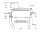
図1は、本発明の処理装置10の断面図である。処理装置10はチャンバ本体12、リッドアセンブリ14及び取外し可能な片持ち式の基板支持部材16を含んでいる。これら部材は組合わされて、基板の処理を行なう真空排気可能な密閉容器及び排気通路22を、物理的及び電気的に対称に形成する。
【0015】
好適には、チャンバ本体12は、機械加工された一体の構造体であり、内側の環状処理領域20を画成し、また、下端部に向かってテーパをつけて同心の排気通路を画成している側壁部18を有している。チャンバ本体12は、スリットバルブ44により密閉される基板入口ポート24と、片持ち式の実装基板支持部材16が配設される側方ポート26を少なくとも含む複数のポートを画成している。基板入口ポート24及び支持部材ポート26は、チャンバ本体12の対向側面部を貫いて配設されていることが好ましい。基板支持部材16の上面とほぼ同じ高さにあるチャンバの側壁部18の対向側面部において、2つの追加側方ポートが配設され、チャンバ側壁部18に形成されたガスチャネル28に接続されている。解離性フッ素含有ガス等のクリーニングガスは、遠隔プラズマ源30からチャネル28内に向かい、そして、そのために設けられ且つ図18に示されるガス入口ポートを介してチャンバ内に導入される。チャンバ内へ通じるポートの開口部の位置は、堆積が大量に生じるチャンバ領域の方にガスを向けるように提供されている。以下、遠隔プラズマ源及びクリーニングガスの送出を、詳細に説明する。
【0016】
チャンバの側壁部18の上面は、リッドアセンブリ34のベースプレート33が支持されているほぼ平坦な着地領域を画成している。その壁部18の上面には、1以上のオー(O)リングの溝部が形成され、チャンバ本体12とベースプレート33との間の気密シール部を形成している。以下、リッドアセンブリを詳細に説明する。
【0017】
基板支持部材16は、チャンバ側壁部18に形成された側方入口ポート26を介して部分的に延び、フランジ46に沿ったチャンバ側壁部18に取り付けられて、チャンバの中央部にほぼ環状の基板収容面200を提供している。支持部材16がチャンバ内に配置されるときは、環状の支持部材16の外壁部50とチャンバ内壁部52とが、支持部材16の周縁部全体にほぼ均一な環状の流体通路22を画成する。ほぼ均等な通路22及び排気ポート54は、支持部材の基板収容面とほぼ同心であることが好ましい。排気ポート54は、支持部材16の基板収容部分の中央下方に置かれ、均等な通路22を通ってチャンバの外にガスを均等に吐出するようになっている。このことにより、基板周縁部全体を囲む基板表面についての均一なガスの流れが放射状に下方に向かい、そして、チャンバのベースの中央に配置された排気ポート54を介して、チャンバから外方に向かって可能となる。均等な流体通路22は、排気ポートに対して異なる近接性を有する基板位置のような、既存のチャンバには欠落している圧力と滞留時間との均等性を維持することにより、薄膜層を均等に堆積することを促進する。
【0018】
チャンバ本体のテーパを付けた下部部分には、ツインブレードスロットルアセンブリ56、ゲートバルブ58及びターボ分子ポンプ60を備えるポンプスタック(pumping stack)が取り付けられ、チャンバ内部の圧力制御を行うようにしている。ツインブレードスロットルアセンブリ56及びゲートバルブ58は、チャンバ本体12とターボ分子ポンプ60との間に設けられて、ゲートバルブ58による分離、及び/又は、ツインブレードスロットルアセンブリ56の設定により決定される0〜13.3Pa(0〜100mTorr)の圧力における圧力制御を許容している。1600L/秒のターボポンプが好適なポンプではあるが、しかしながら、所望のチャンバの圧力を達成することができる任意のポンプを使用することができる。フォアライン(foreline)57が、ターボポンプから上流側及び下流側の位置にある排気ポート54と接続されている。このことは後方排気能力を提供する。フォアラインは、基本的には粗引きポンプであるメインフレーム遠隔ポンプに接続されている。ポンプスタックにはポート59が形成され、フォアラインのフランジ61を取り付けている。チャンバのクリーニング中は、クリーニングガスは高速でチャンバ内に流し、それによりチャンバ内の圧力を増す。したがって、本発明の一態様では、ターボポンプをゲートバルブ58によりチャンバから分離し、クリーニング中はメインフレームのポンプを使用して、チャンバ内部の圧力が維持されるようになる。
【0019】
チャンバ内で基板の処理中は、真空ポンプはチャンバを真空排気し、0.533〜0.800Pa(4〜6mTorr)の範囲の圧力にして、それから、メータで計った処理ガス又はガスの流量を、ガス分配アセンブリを介してチャンバ内に供給する。チャンバの圧力は、チャンバの圧力を直接測定し、そして、排気速度を調整するためにバルブの開閉をする制御装置にこの情報を送ることによって制御する。ガスの流量/濃度は、処理レシピにおいて提供されたソフトウェアの設定値を介して、質量流量制御装置により直接制御する。また、排気ポート54を通ってチャンバの外へ排気されるガスの流量を測定することにより、入口ガス供給源の質量流量制御装置(図示せず)は、チャンバ内の所望の圧力及びガス濃度を維持するために使用することができる。
【0020】
チャンバリッドアセンブリ
基本的に、チャンバリッドアセンブリは34は、エネルギ伝達ドーム32と、エネルギ送出アセンブリ62と、ヒンジ取付けベースプレート33上に支持される温度制御アセンブリ64とからなっている。ベースプレート33は、ガス分配リングが配設される内部環状溝を画成している。ガス分配リングの最上部にはOリング溝が形成されてOリングを収容し、ドーム32及びガス分配リングの最上部を密閉している。組み合わせによっては、リッドアセンブリが、プラズマ処理領域の他にエネルギ送出装置をも共に物理的に密閉して、処理を行うようにしている。好適には、様々な構成部品を収容するために、カバーがリッドアセンブリ全体を覆って設けられている。
【0021】
基本的に、ドーム32は、平坦な最上部68により一端部に対して囲まれた円筒形の側壁部66からなる。円筒形の側壁部は基板支持部材16の上面に対しほぼ直角であり、平坦な最上部68は基板支持部材16の上面とほぼ平行になっている。側壁部と最上部との間の接合部70は丸みを持ち、湾曲したドーム32の内壁部を提供している。ドーム32はRFエネルギに対して透過性のある誘電体材料、好ましくは酸化アルミニウム(Al2O3)、窒化アルミニウム(AIN)又は石英(SiO2)等のセラミックで作られている。
【0022】
独立に電力供給される2つのRFコイル、すなわち最上部コイル72及び側部コイル74は、誘電体ドームの外側に巻き付けられている。側部コイル74は、コイル72とコイル74間の電気的クロストーク(crosstalk)を減らすために、接地遮蔽で覆われることが好ましい。このようなRFコイル72,74は、2つの可変周波数RF電源76,78から電力供給される。
【0023】
各電源には制御回路が含まれており、反射電力を測定し、また、RF発生装置内のデジタル制御シンセサイザを調整し、基本的に1.8MHzから周波数を掃引し始めて、反射電力を最小にしている。プラズマが点火すると、プラズマはコイルと並列な抵抗体として働くので、回路の状態は変化する。この段階で、RF発生装置は、再び最小反射電力点に達するまで周波数を掃引し続ける。電源回路は、最小反射電力点が達成される周波数又はその付近で、各組の巻線が共振するように設計されているので、巻線の電圧は十分に高くなって、プラズマを維持するのに十分な電流を流すことができる。かくして、周波数同調は、処理中に回路の共振点が変化した場合に、装置が共振周波数付近に維持されることを保証する。このように、周波数同調は、インピーダンス整合構成部品(例えばコンデンサやインダクタ)の値を変えることによって、インピーダンスの整合や回路の同調を行なう必要性を取り除いている。
【0024】
たとえプラズマインピーダンスの変化によりインピーダンスの不整合が連続的に変わっても、各電源は、インピーダンスが不整合にもかかわらず所望の電力が負荷に送出されることを保証している。電力を負荷に対して正確に送出することを確実に行うために、各RF発生装置は反射電力自体を分散させて出力電力を増加させ、その結果、送出される電力が所望の水準を維持するようになる。
【0025】
図2(a)、図2(b)及び図2(c)は、独立した3つの局所RF整合部の構成を概略的に示したものである。図2(a)は、コイルLの一方の端部を接地した整合部の構成を示したものである。2つのコンデンサC1,C2はRF分圧器を形成している。図2(b)には、両端の2つの分路コンデンサC2,C3を接地した平衡コイルLを使用して負荷(プラズマ)周波数を整合する。最後に、図2(c)には、コイルLの両端の2つの可変コンデンサを接地したパイ(B)形の整合回路網が用いられている。大抵の従来のRF発生装置の出力インピーダンスは50Ωとなるように設計されているので、整合回路網2(a),(b)又は(c)を使用して、下限が5Ωから上限が900Ωまで(平衡負荷の場合)のインピーダンスの範囲にあるプラズマに最大の電力を伝達することができる。このような2重コイル装置だと、リアクタチャンバ内で半径方向のイオン密度プロファイルの制御が可能となる。
【0026】
図3は、コイルの形状寸法及び最上部コイル72及び側部コイル74のRF給電部を主に示しているチャンバの概略側面図である。図2(c)のところで説明したパイ形回路網の整合装置が図3に示されている。チャンバ13内にはラングミュア(Langmiur)のプローブが導入されて、チャンバ13全体の様々な位置におけるプラズマイオン密度を測定して、最上部コイルのみ及び側部コイルのみを使用してプラズマを発生させることができるようになっている。2重コイルの配置構成が、被処理の基板に適切に同調すると、基板の表面全体には均一なイオン密度をもたらすことができる。基板表面全体でイオンが均一になると、ウェハ上への均一な堆積及びギャップ埋込みの実行の一助となり、不均一なプラズマ密度によってデバイスのゲート酸化物がプラズマで荷電することを緩和するのに役立つ。コイルの動作が重ね合わせられたとき、プラズマ密度が均等に生じ、堆積特性を著しく改善することができる。
【0027】
また、ドーム32には温度制御アセンブリ64が含まれ、様々な処理サイクル中、すなわち堆積工程やクリーニング中にドームの温度を調整するようにしている。図4は、温度制御アセンブリ64及び最上部コイル72の組立分解図である。基本的には、温度制御アセンブリは、相互に隣接して配設される加熱プレート80と冷却プレート82とを備えており、また、好適には、グラフォイル(grafoil)等の熱伝導材料からなる薄層84をそれらの間に配設させている。好適には、約0.102〜0.203mm(約4〜8mil)のグラフォイルの層がそれらの間に配設されている。AINプレートのような熱伝導性プレート86が設けられ、その下面にはコイル72を収容するために溝が形成されている。熱伝導性プレート86と加熱プレート80との間には、好ましくは、厚さが0.025〜0.102mm(1〜4mil)のグラフォイルからなる第2の層88が配設されている。コイル72とドーム32との間には、熱伝導性の第3の層90が配設されている。第3の層は、0.102〜0.203mm(4〜8mil)の厚さを有するチョメリックス材(Chomerics)からなる層であることが好ましい。熱伝導性の層はドーム32との熱伝達を容易にする。クリーニング中はドームを加熱することが好ましい、一方で、処理中はドームを冷却することが好ましい。その結果、熱伝導性の経路が設けられて、これらの利点が達成されるようになる。
【0028】
冷却プレート82には、その内部に形成され、水のような冷却流体が流れる1以上の流体通路が含まれている。冷却プレート内の水路は、チャンバ本体に形成された冷却チャネルと直列になっている。急速脱着継手を備えたプッシュロック式ゴムホースにより、水がチャンバ本体及びリッドの冷却水路に供給される。戻りラインには、インターロック式のフロースイッチを備えた目視流量計がある。流量計は、約60psiの圧力で0.8gpmの流量が得られるように工場で校正されている。ドームには、温度を測定するための温度センサが設けられている。加熱プレート80は1以上の抵抗加熱エレメントを配設させて、クリーニング段階中にドームに熱を供給することが好ましい。好適には、加熱プレートは鋳造アルミニウムで作られているが、しかしながら、この分野で知られている他の材料を使用してもよい。ドームの温度を調整するために、制御装置は温度制御アセンブリに接続されている。
【0029】
構成部品80,82,84,86及び88はそれぞれ、最上部コイル72の端部が延在している2つのチャネルを画成している。加熱プレート80、冷却プレート82及びグラフォイル層に形成された各チャネルには、2つの絶縁スリーブ94,96が配設されて、チャネル内に延びているコイルのリード線を絶縁するようにしている。絶縁スリーブには、その下端部に配設されたシリコン吸引カップが含まれ、絶縁プレート86において密閉をするようにしている。
【0030】
直接伝導により、加熱プレート80及び冷却プレート82を用いて、ドームの温度を制御するようにしている。ドームの温度を±10K以内に制御することにより、ウェハの繰返し精度(wafer to wafer repeatability)や堆積密着性が改善され、また、チャンバ内に落下する破片や粒子が減ることが分かった。基本的に、ドームの温度は、処理要件によって100〜200℃の範囲内に維持されている。また、ドーム温度が高くなれば、より高いチャンバのクリーニング速度(エッチング速度)とより高い薄膜密着性とを得ることができることが示されている。
【0031】
陰極及びリフトアセンブリ
次に、図5〜図10を参照して、陰極及びリフトアセンブリについて説明する。基板支持部材には、チャンバの内部に配置可能なエレメントと、チャンバの外部に配置可能なエレメントとが含まれている。チャンバ内に配置可能な支持部材16のエレメントは、チャンバの側壁部18に設けられた連絡ポート26を通ってチャンバ内部に延び、チャンバ外部に配置可能なエレメントにより側壁部に支持されている。図5は基板支持部材16の断面図である。支持部材16は、チャンバの壁部に取り付けるためのフランジ46を有するベース94、半径方向に内向きに延びている片持ち腕部分96、及び片持ち腕部分96の端部に配置された基板収容部分98を備えている。フランジ46は、基板支持部材連絡ポート26の周囲のチャンバの壁部18に、支持部材のベース94を取り付けるものである。ベース94はフランジ46から内方に延び、片持ち内壁部分51を画成している。片持ち壁部51は弓形をなすもの、又は、チャンバの全体にわたる内径(R)とほぼ等しい半径(r)を有する円弧であることが好ましい。周方向の片持ち壁部51の表面は、チャンバの内壁部52に隣接して収容されている。支持部材16が図7に示されるように処理用のチャンバ内に配置されているときは、片持ち壁部51がチャンバの内壁部52と共に、対称的且つ連続的なチャンバ内壁部を形成する。
【0032】
片持ち腕部96はベース94の下方部分から内側に向かって延びて、基板収容表面99を有するESC収容部分98を支持している。ESC収容部分98は、上方に延びている環状のパイロット100を含んでいる。環状パイロット100には大内径部分と小内径部分とがあり、内部環状段を形成して絶縁部材102が支持されるようになっている。絶縁プレート102上にはESC104が支持されて、基板収容表面99が設けられることが好ましい。ESC収容部分98の外壁部50は環状面を連続的に画成している。
【0033】
また、ESC収容部分98には、基板位置決めアセンブリ110が配設されている凹部108が画成されている。収容部分の下方部分には、底部プレート112がねじを配置することにより固定され、支持部材16の内部構成部品が処理環境から保護されるようになる。
【0034】
図7は、チャンバ内に配設された支持部材16を示す断面平面図である。片持ち腕部96は対称的な流体通路22を横切って延び、チャンバ内でESC収容部98を支持している。片持ち腕部は、半径方向の通路等の1つの通路又は複数の通路114を含むことにより、流体通路22を通る流体の流れの遮断、制限又は妨害を最小限に抑制していることが好ましい。また、支持腕部116は、その内部に1以上の通路118を含んで、均等な流体通路内の流体の遮断、制限又は妨害を最小限にしていることが好ましい。
【0035】
さらに、流体が片持ち腕部の内部及びその付近を通過するときに流体の遮断、制限又は妨害によって生じる基板表面付近のガスに対する影響をさらに最小にするために、片持ち腕部96がESC収容部分98の基板収容表面から離れた位置、例えばESC収容部分98の底部に沿った位置等に取り付けられていることが好ましい。より基本的には、配置された基板の上の流体の流れに対する影響を回避するために、流体通路22内の不均等性が最小限にされ、且つ、ESC収容表面98から十分な距離を置いて配置されることが好ましい。
【0036】
基板リフトアセンブリ120には、半径方向に延びている複数の支持ピン122が含まれており、ESC収容部材98の周囲に間隔をおいて配列され、且つ、ウイング形取付プレート123上に収容されている。取付プレート123は、支持部材16に形成されたほぼ矩形の凹部内に配設されており、垂直方向に移動可能なエレベータアセンブリ126によって動かされるようになっている。図5に示されるように、エレベータ機構126は、上端部に取付プレート130を取り付け、垂直方向に移動可能なシャフト128を含んでいる。シャフト128はアクチュエータ、好適にはチャンバの外部に配置される空気圧シリンダによって垂直方向に上下に移動するものになっている。
【0037】
支持ピン122は、ESC収容部材98を垂直方向に通って配設された穴部134の中に設けられたスリーブ132内に収容されて、密閉容器内の支持部材16とは独立に移動するようになる。支持ピン122が支持部材16から延びて、ロボットブレードが基板をエンクロージャから取り出すことを許容しているが、ESC104の上面に基板を配置するためには、各ピンは支持部材16の内部へ下降しなければならない。ピンにはそれぞれ円柱状のシャフトが含まれており、周縁下部分及び周縁上部分で末端をなしている。
【0038】
次に作用について説明する。外部ブレード138が(被処理の基板を支持し)スリットバルブ24を介してチャンバ内に挿入するようにして、支持部材16の上に基板を配置する。適切なブレード138及び基板を運搬する関連のロボット装置の例の1つが、ダン・メイダン(Dan Maydan)、サッソン・ソメク(Sasson Somekh)、ディビット・ケー・ウォン(David N.K.Wang)、ディビット・チェン(David Cheng)、マサト・トシマ(Masato Toshima)、イサク・ハラリ(Isak Harari)及びピータ・ハップ(Peter Hoppe)の名前で出願され、発明の名称が「マルチチャンバ統合処理装置(A Multichamber Integrated Process System@)」である、本願と同一人に譲渡された同時係属出願第944,803号に記載されており、これは参考として本明細書で援用されている。エレベータ機構126は基板支持ピン122をブレードより上に上昇させ、基板を持ち上げる。次に、ブレードをチャンバから引っ込め、空気圧シリンダがブレードアクセススロット上のドアを閉じて、チャンバを密閉する。エレベータ機構126を動かして支持ピン122を下降させ、処理のための所定の位置である支持部材16の上面98に基板を収容する。
【0039】
処理後は、エレベータ機構が支持ピン122を上昇させて基板を持ち上げ、基板支持部材16から離す。次に、ドアを開け、ブレードを再びチャンバ内に挿入する。次に、エレベータ機構126は基板支持ピン122を下降させ、基板をブレードに置く。下方に移動したピン122がブレードを取り除いた後に、ブレードを引っ込める。
【0040】
処理中は、CVDの処理環境のプラズマが大量の熱を発するが、プラズマによって発生する総発熱量は、プラズマの電力密度に少なくとも部分的には依存している。このような熱の一部は基板に伝わるので、所定の臨界温度以下に基板の温度を維持するために、基板からこの熱を除去しなければならない。このような熱を取り除くために、基板支持部材16には伝熱装置が設けられて、支持部材及び被処理の基板の温度が制御されるようになっている。図6は、支持部材の伝熱装置を示す断面平面図である。取水部140及び排水部142は通路144,146により接続されている。支持部材16の内部には給水マニホールド148が配置されて、支持部材から冷却流体への熱伝達を促進するようにしている。支持部材16の温度を選択して、チャンバの処理領域から上流のガスマニホールド内部で早期に堆積することを回避している。基板支持部材16全体の至る所に収容されている冷却チャネル144,146は、冷却流体の通路用に設けられたものである。さらに、ESC104(以下で説明する)の表面にあり、ガスが流れる溝部が、熱を基板から支持部材16内に、そして実質的には冷却流体内に伝達している。
【0041】
図8は、本発明にしたがった静電チャック104の一実施形態の平面図である。図8(a)は、ウェハの平坦部を除去して対称的になっている他の実施形態である。平滑な最上面を有しているのではなく、多数の溝が多数の突起部166を形成している表面に設けられている。これら突起部の中央領域168は、シール部172により周縁領域170から分離されている。シール部172は、溝部をその中に形成して突起部を設けていない領域にすぎず、このため、分離した領域間の流れを最小限にするための固体表面が形成される。外側シール部174は、チャンバ内にヘリウムガスが漏れることを最小限にするための障壁を提供している。
【0042】
ヘリウムガスが周縁領域170の中に向かって、一連の穴部をその中に有する溝部となっているリング176を介して挿入され、図1のヘリウムのライン47から当該領域に向かって高圧ヘリウムが収容されるようになる。内側リング178は、ヘリウム圧力ライン147から中央領域168へ向かう低圧ガスを許容している。次に作用について説明する。中央領域168においてヘリウムによる初期の低圧を設定した後に、ヘリウムリング178がシール領域172を介して漏出するヘリウムガスを除去して、所望の低圧へリウムが維持されるようにすることが基本的である。他の実施形態では、リフトピンの穴部になりうる真空穴部180が用いられ、図1の真空排気ライン135を使用して中央領域のガスを真空排気し、中央領域の圧力をさらに低めることができる。或いは、追加の真空穴部を付加してもよい。
【0043】
ヘリウムの溝部178は、シール領域172付近に配置されていることが好ましい。それをできるだけ近くに配置することにより、所望の伝熱の階段関数に近付けることができる。このため、高圧ガスは、周縁部のそばの狭い領域内に収容される。高圧ガスが遠く離れてウェハの中央部に向かって延在してる場合に、冷えた中央部が一層冷えれば冷えるほど、ますます高圧になるガスによって生じる熱の差分の低下を部分的に相殺するようになる。
【0044】
次に作用について説明する。ウェハを加熱するために、低圧のヘリウム(133〜2000Pa(1〜15torr))を中央領域168に供給し、また、高圧のヘリウム(133〜2666Pa(1〜20torr))を周縁領域170に供給する。周縁領域の高圧ヘリウムを高圧にすればするほど、ウェハの周縁部においてより良好な熱伝達が行われる。
【0045】
実施形態の中には、シール部が静電チャック164の残りの部分と同じセラミックコーティングで作られているものがある。上述のセラミックコーティングでは隙間が小さくなっており、このため、シール領域では完全な密閉が提供されない。さらに、基板すなわちウェハには裏面が多少粗いものや、基板サポートより粗いものがある。したがって、シール領域は十分な幅を有して、一の領域から他の領域にヘリウムがかなり漏出することが防止されるようにすべきである。静電チャックがセラミックで覆われた場合、圧力範囲が上述されているときには、シール幅が2.54mm(1/10インチすなわち100mil)であることが効果的であることが試験により確認された。好適には、シール幅は1.27〜7.62mm(50〜300mil)の範囲内にある。外側シール部174の場合は、幅を最小にすることが好ましいが、なぜならば、このシール部より上のウェハ領域に、高圧ヘリウムからの熱伝達の利点がないからである。同時に、シール部は十分な幅になって、ヘリウムがチャンバ内にかなり漏出して、高い流量レベルによりヘリウムの持続圧力に達することにより意図した熱伝達能力を損なったり、チャンバ内の反応に影響を及ぼすおそれのあることが防止されなければならない。前述の2.54mm(100mil)の幅が効果的であり、最適なシール幅が1.27〜7.62mm(50〜300mil)であることが分かっている。基板サポート及び基板の材料や平滑度が異なる場合は、別の幅が適切であるかもしれない。例えば、よく知られた多くの供給者から入手可能なKaptonJ等のポリマの膜を使用する場合には、それに応じるために小さい幅のものを持ってきてもよい。
【0046】
好ましい熱伝達ガスはヘリウムであるが、なぜならば、それは不活性であり、比較的安価であるからである。或いは、アルゴン、酸素、CF4若しくはその他のガスを使用したり、又は、混合ガスを使用したりしてもよい。例えば、圧力制御の追加能力を提供するための混合物を使用してもよい。特定のガスを選択してチャンバ内の化学処理と両立できるようにし、漏れガスが化学反応に対して影響を最小限にするようにすることができる。例えば、エッチング種としてフッ素を使用するエッチング反応では、裏面熱伝達ガスとしてCF4を使用することが望ましい。
【0047】
熱伝達は主としてヘリウムガスを介して行われるので、かかる目的のためにシール面積と突起部の大きさ及び数を最小限にすることが望ましい。したがって、基板の面積における接触面積が非接触面積より小さくする必要がある。他方、シール部はガスの漏れを防止することが必要とされて、突起部はウェハを機械的に支持するために十分な大きさと間隔を有していなければならない。さらには、最適化すべきその他の要素がある。突起部間において基板と基板サポートとの間のギャップを決定する突起部の高さは、ガスが処理開始時間に影響を与えることなく、迅速に領域全体に分配されるようになることをできるよう十分になっていなければならない。基本的には、これはおおよそ数秒でなければならず、好適には10秒以下でガスが分配されている。
【0048】
熱伝達が最適となるためには、ギャップは十分小さくなり、別のガス分子と衝突することなく基板から基板サポートに直接移動する分子によって、熱伝達が主として行われ、自由分子の熱伝達を行う必要がある。したがって、ギャップはガスの平均自由行程(混合ガスを使用する場合は自由行程の平均値)より小さなっている必要がある。平均自由行程は、ガスの圧力と分子衝突断面積との関数である。様々な圧力を使用すると、平均自由行程は変化する。好適な実施形態では、適用される最大圧力の平均自由行程を用いてギャップの寸法を決定する。
【0049】
さらに、誘電体の全厚に対するギャップの比率を小さくして、基板の局所的な異常を回避する必要がある。この比率が有意なものとなれば、空間と突起部間の等価キャパシタンスが著しく変化し、かなり異なる電界が基板に印加される。このように電界が異なると化学処理に悪影響を及ぼし、堆積、エッチング、ドーピングされたり、又は、その他の属性変化を受けたりする薄膜に不均一性が発生する。多少の差は必ず存在するが、これを最小限に留めることが望ましい。
【0050】
また、この比率の有意性は、誘電体材料によって、特に材料と熱伝達ガスの誘電率の差(基本的には同一)によって異なる。2つの誘電率が近ければ近いほど、ギャプが大きくてもその重要性は小さくなる。
【0051】
ギャップの大きさを設定する際の他の重要な点は、基板サポートとウェハの裏面との間の熱伝達ガスによりプラズマを発生させることを回避することである。これは、ギャップの大きさが熱伝達ガスの平均自由行程の数倍になると、重要になり始めると考えられている。
【0052】
静電チャックの一実施形態の場合、セラミックコーティングの厚さはおおよそ0.178〜0.254mm程度(7〜10mil程度)になっている。KaptonJを使用した場合は、0.025〜0.051mm(1〜2mil)の厚さを使用することができる。チャックの目的を得るために、誘電体は、製造の一貫性を維持し且つ絶縁破壊を回避する範囲内でできるだけ薄くなっていることが理想的である。上に述べられた2つの領域の圧力でのヘリウムの平均自由行程は、約0.025〜0.127mm(約1〜5mil)となる(非常に高い圧力では、平均自由行程はこれより小さくなりうる)。したがって、0.017〜0.030mm(0.7〜1.2mil)の突起部の高さが選択され、試験されて、効果的であることが明らかになった。これにより、所望の圧力においてヘリウムの平均自由行程より小さいギャップが与えられる。好適には、当該ギャップは、妥当な(pertinent)圧力において熱伝達ガスの平均自由行程の2倍以下であることが好ましく、より好適には平均自由行程以下になっている。
【0053】
突起部間の間隔は、湾曲することなく基板が支持されている限り、できるだけ大きくなっている。一の実施形態では、基板が平坦に維持されているが、一方、他の実施形態では、突起部の高さ或いは基板サポートの最上面を変えて(突起部の高さを均等にし)、湾曲した基板を適切に支持することが望ましい。別の要素として、電界の局所的異常の原因になる尖鋭な点を回避することがある。間隔が大きいと、チャックを解除するときの電荷の移動にも影響を与え、破損の原因になる可能性がある。
【0054】
突起部の最適な中心距離は2.54〜7.62mm(100〜300mil)の範囲内にあり、好適には約7.62mm(約300mil)になっていることが明らかになっている。好適には、突起部自体の大きさは直径で0.254〜3.81mm(10〜150mil)の間にあり、より好適には約3.30mm(約130mil)になっている。矩形の突起部が示されているが、単にそれらが製造しやすいからであり、他の形も同様に使用することができる。例えば、環状のものを使用することができる。
【0055】
図示実施形態では、ガスを除去するための開口部が外側周縁領域に示されていないが、他の実施形態ではこれが設けられていてもよい。ヘリウムの圧力の制御は、高圧又は低圧ヘリウムを使用したり、又は、真空ポンプによって真空排気したりすることによってなされうる。同様に、中央領域の場合は、圧力はこれらの方法のいずれか又は両方の組み合わせで制御されうる。サポートの中央部に近接した真空部と組み合わせて、ヘリウム供給源を縁部に近接したリングとして配置することにより、中央領域内には追加の圧力勾配が生じ、中央部に向かって低下する。例えば、本発明の他の実施形態は、この方法により2つの圧力領域を通して熱伝達の粗調整をし、中央領域におけるヘリウム入口及び真空出口を配置することにより微調整を実施する。他の実施形態では、2以上の領域を使用してさらに細かい微調整を行って、より多くのハードウェアを必要とすることが引き換えになることができる。
【0056】
図9は、誘電体186の変化している厚さを示しているESC104の一実施形態の側面図である。ウェハ182はチャックに取り付けられて示されている。チャックは、誘電体186で覆われた電極部分184を含んでいる。誘電体は、静電チャックの最上部全体及び側部190に沿って延在している。理解されるように、誘電体は中央部分で厚く、また、周縁部分194では薄くなっている。この側面図は複数の突起部170を示しており、さらに、内側シール部172及び外側シール部174を示している。
【0057】
周縁部分194で誘電体が薄くなっているほど、これらの部分により強い静電力を与える。これは多くの理由により都合のよいことになっている。第1に、それがウェハをしっかりと保持して、静電チャックの最上面とより良好な接触をすることにより、より良好な熱伝達を確保している。第2に、力がより強くなると、周縁部に近接したシール部172とシール部174との間の高圧のヘリウムを抑制するのに役立つ。さらに、ウェハの周縁部分が中央部分と異なる温度を有している場合には、これにより、それが中央部分に比べて湾曲するおそれがあり、しかも、上向き又は下向きに湾曲するおそれがあり、熱の差分の問題がさらに悪化する。このことは、周縁部分で静電力が適切に高められることによって克服することができる。
【0058】
他の実施形態では、2つの圧力領域なしで又は突起部なしで、誘電体の変化する厚さを用いることができる。誘電体被膜の変化は連続的になっていたり又は階段形式になっていたりしてもよい。階段形式との差は製造を容易に且つ安価にしている。
【0059】
シール領域174と、ウェハの縁部の静電力が強くなることとに関する他の利点は、静電チャックの最上面に近接して露出した金属に対するプラズマ放電を防止することである。基本的には、上述の露出した金属はヘリウムの入口ポートにあり、アルミニウム電極を介して近づき(come up)、このため、これらの穴を通って電極に通路が露出する。放電は、より気密なシール部を設けるか、ヘリウム入口穴部を静電チャックの縁部から十分に離れた位置に配置するか、又は、そうした放電を防止する溝をそこに設けることによって防止される。
【0060】
図9に示されるように、静電チャックの最上面とウェハとの間の空間には、温度センサ196が設置されうる。こうして、温度センサからウェハの温度を推測することができる。
【0061】
図10は、温度制御を例示しているフィードバック制御装置の信号の系統線図である。図10の線図は、ヘリウムの圧力を制御するための閉ループ温度制御装置用のものである。或いは、温度センサのない開ループ装置を使用してもよい。事前の実験により所望のプロセスパラメータに対して、適切なヘリウム圧力が表されることができ、したがって、他の実施形態では温度センサを除去することができる。図9は、プロセッサ内で実行される関数と物理的効果とを両方含むものである。
【0062】
温度設定値は、メモリ245の制御プログラムから制御装置へのユーザプログラムの入力として提供される。温度設定値は制御装置によって定数198を乗じられて、その結果が、加算関数202で示されるように、帰還信号213に加算される。加算関数の結果は制御装置により使用され、ヘリウム供給源の流量抑制装置(flow restrictor)又はバルブを制御することにより、ヘリウムの圧力を制御する。これにより、ヘリウムガスの熱伝達の程度が変化する。好適な実施形態では、ヘリウムの圧力は数学的なモデルにしたがって制御されるが、しかしながら、圧力制御の基礎として経験に基づく結果を使用することもできる。以下、数学的なモデルを説明する。ヘリウムの圧力は、ブロック202で示すように、ESCへの熱伝達を制御する(或いは、任意の形式の基板サポートを使用してもよい)。ESCは熱交換器233で冷却されたり、又は、加熱器243で加熱されたりして、ウェハへの熱の伝達の量がヘリウムの圧力によって制御されている。このような熱伝達は、(ブロック206で示されるように)ESCへの熱伝達と結合し、プラズマから伝達されるエネルギによって発生する(ブロック204で示されるような)熱で相殺することができる。(ブロック208で示されるような)ウェハのサーマル・マス(thermal mass)に適用される全熱伝達により、ウェハの温度210が作り出される。半導体ウェハではなく他の基板を使用してもよいことに留意されたい。また、ウェハの最終温度210は、フィードバック線211で示されるように、静電チャックへの熱伝達量に影響を及ぼす。ブロック202に示されるESCとウェハとの間の熱伝達関数は、ESCの温度の関数の他にウェハの温度の関数である。図示のように、ESCへの熱伝達がウェハからの熱を除去するが、同時に、プラズマからの熱はウェハに加わる。しかしながら、静電チャックを使用してウェハを加熱するときは、これらを逆転させることができ、したがって、熱入力が行われ、同時に、低温のプラズマにより又は単にプラズマが存在しないチャンバにより熱が除去される。
【0063】
ブロック212は、温度センサによって温度が電気信号へ変換されていることを示している。ブロック214は、温度信号をフィードバック信号として温度設定値と結合する前にプロセッサに適用された伝達関数を示している。上述の伝達関数は、最も単純な形では1となる可能性のある定数の乗算、又は、単にアナログ信号からデジタル信号への変換するものとなる傾向がある。
【0064】
制御装置によって実施される関数は、メモリ245内のプログラムの制御によって行われる。そのプログラムは様々な段階を実行するための命令、例えば、温度センサから温度の指示を読み取るための命令や、その温度を所望の入力設定温度と比較するための命令、及び、圧力バルブ(又は流量抑制装置)を制御してガスの圧力を変化させ特定の圧力領域にするための命令等を含んでいる。故障等が発生した場合には、ガスを遮断する他の命令が規定されている。
【0065】
ヘリウムの圧力は、1つの簡単な圧力の静電チャックを使用している場合に、その圧力を増したり減らしたりすることによって、制御することができる。或いは、本発明の好適な実施形態のように2つの圧力領域を使用する場合には、外側及び内側のヘリウム圧力を独立に制御することができる。例えば、各領域の温度は、2つの領域の交差部付近に配置されている単一の温度センサから推測することができる。或いは、2つの異なる温度センサを使用することもできる。他の実施形態では、温度センサが静電チャックの最上面に取り付けられたり、又は、ウェハ自体に直接接触されてもよい。例えば、圧力の変動を発生させる漏れが領域間にある場合には、その圧力を推測するために温度センサを使用してもよい。ウェハから多少離れていることが基本的であり、その下では異なる圧力を有している可能性のあるその出力部における圧力のみを、圧力調整器は検出している。温度センサは、ウェハの下の実際の圧力を推測するために使用することができる。ウェハ表面の粗さによっては、漏れ量が変動することがあり、供給する圧力を変動させる必要があるかもしれない。
【0066】
制御装置はそれに対して特定の制限をすることが基本的である。例えば、ヘリウムの圧力は、ウェハが静電チャックから持ち上げられて離れないように、又は、圧力差が大きくなり熱応力のためにウェハが破損する熱勾配を発生するように、制限される。上述の制限を超えたり又は画成されたその他何らかの障害が発生すると、ガスの流れは停止する。
【0067】
プロセスキット
プロセスキットはカラー及びカバーからなる。さらに、スカートを使用してもよい。セラミックのカラーはウェハの大きさ及び種類によって異なり、静電チャックと石英カバーの間に配設されている。カラーの主な目的は、静電チャックのフランジをプラズマの影響から保護することである。カバーはカラーから陰極アセンブリの外側周縁部まで延びており、その主な目的は、陰極アセンブリをプラズマの影響から保護することである。スカートは、上部チャンバ及び下部チャンバを密閉するスペーサ及びOリングを、プラズマの影響から保護するために、下部チャンバに配設してもよい。
【0068】
一の態様では、本発明は、ガス生成物の堆積を防止又はそれに耐える半導体処理チャンバの静電チャック用の改良型のプロセスキット又はシールドを提供している。さらに、このシールドは、酸化物の堆積物を高速で除去し、その結果、ウェハ製造工程のスループットが向上する。
【0069】
一の実施形態では、カラー又はカバーには、1以上の表面又は内部に配設された導電材料が含まれて、その表面のクリーニングが高められてもよい。総括的には、誘電体のドーム32の周囲に配設されている誘導性コイルを使用して、カラー又はカバーの導電材料を加熱し、それからカラー又はカバーの表面を加熱するようにしている。フッ素系の化学薬品又はその他の反応ガスを使用してなされるその場のクリーニング工程が、高温で強化されることが示されている。プロセスキット部品に配設された導体と誘導性コイルとを使用することにより、これらの部品の表面の温度が上昇し、クリーニング速度が増す。
【0070】
一例として、電流を誘導することのできる導体を設けるために、カラーやカバー等のプロセスキット部品の一表面に金属を堆積することができる。加熱処理の操作は、コイルを外部巻線、金属層を内部巻線とする変圧器において見られるものと同様である。
【0071】
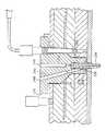
図11は、静電チャック及びプロセスキットの断面図である。基板サポートアセンブリ230には、高いサーマル・マスと優れた熱伝導率を有する導電材料から一体的ブロックとして好適には製造される支持体232が備えられ、その上面について冷却されるウェハから熱の吸収を促進するようにしている。アルミニウム又は陽極酸化されるアルミニウムが、支持体232の好適な材料であるが、なぜならば、それは約2.37W/cm-ECの高い熱伝導率を有し、また、それは半導体ウェハと両立できる工程であることが基本的であるからである。支持体232は、ステンレス鋼やニッケル等他の金属を備えていてもよく、また、支持体232は、追加の非導電材料を備えていてもく、又は、支持体全ては、非導電性若しくは半導性の材料を備えていてもよい。他の実施形態では、支持体232はセラミックからなる一体プレートを備えている。このような構成では、セラミックプレートは導電性エレメントが含まれ、その内部に埋め込まれている。導電性エレメントは、金属エレメント、グリーン・プリンテッド・メタライゼーション(green printed metalization)、メッシュ・スクリーン等を備えていてもよい。支持体232は、支持体232の外表面から外側に向かって延在している環状の取付フランジ234を画成している。好ましくは約700Vの電圧が、基板サポートアセンブリ230に直流電源(図示せず)により印加され、ウェハWを支持体232の上面に近接して保持する静電引力を発生させるようにしている。
【0072】
図11を参照すると、基板サポートアセンブリ230には、支持体232の上面238を覆う平滑な誘電体材料の層236が備えられて、ウェハWの下面を支持している。誘電体層236は、4つのリフトピン穴240の上の領域を除いて、支持体232の上面238全体を覆っている。好適には、誘電体層236は、支持体232の上面234にプラズマ溶射された、アルミナ、酸化アルミニウム又はアルミナ/チタニア複合物の(好ましくはおおよそ約0.10〜0.30インチ程度の)薄いセラミック誘電体層を備えている。
【0073】
一の実施形態では、シールド242は、カラー246の下に位置する導電材料244からなる薄い環状体(annulus)を備えている。カラー246は、環状のフランジ234により支持され、カバー248により保持されている。カバー248は、チャンバをクリーニングするのに必要とされる時間を短縮するために、支持体232の側方の表面を覆って保護するセラミックの外部ジャケットであることが好ましい。カラー246は、小さな間隙250により環状フランジ234から分離されていることが好ましい。間隙250は、環状フランジ234の上面及び導電材料244の下面又はカラー246の自然な表面粗さによって作り出されている。間隙250は、0.0127〜0.127mm(0.5〜5mil)の厚さになっていることが好ましい。処理チャンバが比較的低圧(基本的には約0.667Pa(約5mTorr程度))な環境にあるときには、間隙250は、カラー246と支持体232との間の熱伝導を防止する熱的障壁となる。
【0074】
図11に示されるように、カラー246は、支持体232の直径より大きい内径を有して、両者の間に他の間隙252を画成していることが好ましい。間隙252は、支持体232が処理チャンバ内で加熱されたときに支持体232が膨張する機会を提供し、さらに、基板サポート230又はカラー246に損傷を与えることなく、シールド242を取付けたり及び取外したりすることができること確実にしている。カラー246は、絶縁性換言すれは誘電性の材料からなり、好ましくはセラミック、すなわち、処理チャンバ内にあるウェハ上部のプラズマが静電チャックの一部に接触して浸食するのを防止又は抑制するのに役立つセラミックからなっている。しかしながら、カラー246は必ずしも絶縁材料に限定されず、実際、本出願人は、半導体材料でできているカラー246が、静電チャックをチャンバ内のプラズマから効果的に保護できることが明らかにしている。
【0075】
カラー246は、処理チャンバ内でガスからの堆積物にさらされる、湾曲した上面256を有する薄いリング254である。好適には、カラー246のサーマル・マスに対する露出上面256の面積の比は高くなっており、基本的には約0.1〜5cm2K/Jであり、好適には約1〜1.6cm2K/Jになっている。カラー246のサーマル・マスに対する露出表面の面積の比が高ければ、チャンバ内のRFエネルギによりかなり高温にそれが加熱される。酸化物の堆積速度は、処理チャンバの表面の温度に反比例することが基本的であるので、カラー246が受ける熱は、露出した上面の酸化物の堆積を抑制する。したがって、カラー246の形状は(すなわちサーマル・マスに対する露出した表面の比が高いことは)、上面256の堆積速度を最小にする。
【0076】
堆積工程中、処理ガスからの酸化物は、ウェハWや、エンクロージャの内壁部やカラー246の上面256のようなチャンバの露出した表面のかなりの部分に堆積する。カラー246のサーマル・マスは、表面256の面積に比較して相対的に小さいので、カラー246は比較的大量の熱をRF電源から受け取る。さらに、カラー246は、RF電力を介して熱が発生する導電材料244からなる薄い環状体から加熱される。これにより、上面72への酸化物の堆積速度はさらに低下する。
【0077】
図11に示されるように、ウェハが誘電体層236の上面にあるとき又はそれに隣接しているときに、カラー246は、カラー246の上面がウェハの上面より低く配置されるような大きさで作られていることが好ましい。カラー246をウェハの上面より低い位置に配置することにより、上面256へ酸化物が堆積する速度がさらに低下し、ウェハ縁部への視線が改善される。したがって、ウェハの縁部は、シールド242が仮にウェハよりも上に延びる場合よりも高い堆積速度を受ける。このことは、処理中に生じるのが基本的であるウェハ中央部の高い堆積速度を補償するためには都合のよいことである。
【0078】
処理チャンバのプロセスキットの断面図である図12を参照すると、誘導性のHDP源のソースRFコイル260を用いて、セラミックのプロセスキットを加熱することができる。導電材料244の薄い環状体は、セラミックのプロセスキットの1以上の表面又はその内部に配設されうるが、変圧器の二次コイルとして機能して、ソースRFコイル260のRF電流によって誘導される電流を通し、プロセスキット用の熱を発生させる。2次コイルの抵抗は非常に重要となるが、なぜならば、抵抗が低すぎたり高すぎると電力伝送が不十分となり、したがって、プロセスキットの加熱が不十分となるからである。
【0079】
図12に示す円形の形状の場合、抵抗Rはほぼ2BrD/W@dとなる。ここで、rは導電材料の薄い環状体の外径の半径方向寸法の大きさであり、wは導電材料の幅、dは導電材料の厚さ、Dは導電材料の抵抗率である。抵抗Rは、w@dすなわち導電材料244の断面積を変化させることによって、制御することが好ましい。カラー246との最適な接触を達成するために、wはできるだけ大きく、しかしカラー246の幅より小さいことが好適である。dの最適値を得るための1つの好適な方法は、導電材料の厚さdが異なる場合において、様々な試料の加熱速度を経験的にモニタすることである。一の実施形態では、環状体が10cmの内径、12cmの外径及び0.13mmの厚さを有している状態で、導電材料としてのグラファイトを有しているプロセスキットを約288ECの温度まで誘導加熱した。
【0080】
本発明の他の態様では、プロセスキットのクリーニング速度すなわち堆積除去速度は、温度の関数である(つまり処理中に遮蔽が高温になるほど、短時間にそれはクリーニングすることができる)ことが基本的である。クリーニング中、導電材料244は、ソースRFコイル260内のRF電流によって誘導される電流を通す変圧器の2次コイルとして機能し、プロセスキットのための熱を発生する。したがって、温度が高くなると、カラー246のクリーニング速度は高くなり、装置2の停止時間を短縮し、それによりプロセスのスループットを向上させる。
【0081】
ガス分配アセンブリ
以下、図13〜図16を参照して、ガス分配アセンブリ300について説明する。図13は、ガス分配アセンブリ300を示す本発明のチャンバの断面図である。総括的には、ガス分配装置は、ドームの下部部分とチャンバ本体の上面との間に配設されている環状のガスリング310と、ドームの最上部を通って配置されると共に中央部に配置された中央ガス供給部312とを備えている。ガスは、ドーム32の底部に近接して配置されると共に周方向に取り付けられたガスノズル302,304と、ドームの最上部プレートの中央部に配置される中央配置のガスノズル306との両方を通って、チャンバ内に導入されるようになる。この構成の利点の1つは、ノズル302,304,306を介してチャンバ内の選択位置に、複数の様々なガスを導入することができることである。さらに、酸素のような他のガス又は混合ガスを、ノズル306の周囲に配設されたガス通路308を通して、側部のノズル306に沿って導入し、且つ、チャンバ内に導入される他のガスと混合することができる。
【0082】
以下、ガス分配リング及び中央部に配置されたガスマニホールドを、それぞれ説明する。
【0083】
基本的に、ガス分配リング310には、アルミニウム又はその他の適切な材料314でできた環状リングが備えられ、複数のポートを形成してノズルが収容され、また、1以上のガスチャネル316,318と連通している。好適には、少なくとも2つの別個のガスをチャンバ内に供給するために、ガスリング内に少なくとも2つの別個のチャネルが形成されている。ノズルを収容するためのポートはそれぞれ、リング内に形成されたガス分配チャネル316,318のうち少なくとも1つに接続されている。本発明の一実施形態では、1つおきのポートがチャネルの1つに接続され、同時に、残りのポートは残りのチャネルに接続されている。このような構成では、一例として、SiH4及びO2等の別個のガスを別個にチャンバ内に導入することができる。
【0084】
図14は、ノズル302を内部に配設した1つのポート314に接続されている第1のガスチャネル316を示す断面図である。図示のように、ガスチャネル316は、チャンバ本体の壁部の上面に、好適には、チャンバの壁部の周縁部全体を取り囲んで環状に形成されている。環状のガスリングには、リング内において長手方向に第1の組のチャネル320が配設され、ガスの分配のためにチャネル内に設けられたポート314のぞれぞれに接続されている。ガスリングをガスチャネルの上に配置されるときは、通路がチャネルと連通する。ガス分配リングは、チャネルから外側に配設された2つの別個のOリング322,324により、チャンバの壁部の最上部表面で密閉され、ガスがチャンバの内部に漏れるのを防止する。チャネルの内側の凹部328には、テフロンシール326等が配設され、チャンバへのガス漏れを防止している。
【0085】
ポート314内に配設されたノズル302,304はねじ山を作り、ポートのねじ山と合わせて、両者間の密封をし、また、迅速且つ容易な交換をすることが好ましい。各ノズルの端部に制限オリフィス330を配置して、チャンバ内に所望のガス分布をもたらすために、選択することができる。
【0086】
図15は、第2のガスチャネル318を示す断面図である。第2のガスチャネル318は環状のガス分配リングの上部部分に形成され、また、同様に、ガス分配リングの周縁部を取り囲むように環状の構成をなして配設されている。水平方向に配置された通路332は、ガスリング内に形成された1以上のポートに、第2のガスチャネルを接続しており、そしてここで、追加のガスノズルが配設されている。上部を含んでいる第2のガスチャネルの表面は、ドーム32を支持しているリッドの部分により形成され、また、最上部においてベースプレート33によって密閉されている。ガスリング310は、チャンバ本体にヒンジで取り付けられたベースプレート33にボルト固定されている。
【0087】
本発明の利点の1つは、ガスの分配パターンを調整することができるように、リングがポートを形成して様々な角度でノズルの先端部を収容し位置決めするときに、ガス分配リングを容易に取り外したり交換することができることである。換言すれば、ある適用分野では、リングにポートを形成し、ガスノズルの幾つかをチャンバ内で上方に向けたり、又は、逆にそれらの幾つかをチャンバ内で下方に向けたりすることが有利になっている。ガス分配リングに形成されたポートは、機械加工され、所望の角度を選択して所望の処理結果をもたらすことができるようになっている。さらに、少なくとも2つのガスを別個にチャンバ内に送り込むことができる少なくとも2つのガスチャネルがある場合は、様々なガスの間で発生する反応の際立った制御をすることが可能になる。さらにまた、ガスを別個にチャンバ内へ送り込むことにより、ガス分配アセンブリ内のガスの反応が防止されることができる。
【0088】
図16は、ドーム32を通って配設された中央ガス供給部312を示す断面図である。最上部ガス供給部312は、ドームの最上部に配設されたベース334と、ドームに形成された凹部内に配設されたテーパボディ336とを有するテーパ構体になっていることが好ましい。別個の2つのOリング336,338は、1つがテーパボディ336の下面とあり、また、1つが下端に向かったテーパボディ338の側部表面にあるとき、ガス供給部312とチャンバのドームとの間の密閉可能な接触をしていた。最上部ガス供給部の本体の下部部分にはポート340が形成されて、ガスをチャンバに送り込むためのノズル306が収容されるようになっている。少なくとも1つのガス通路342が、ポートに接続されたガス供給部310の至る所に配設され、ガスがノズルの後部まで送り込まれるようになる。さらに、ノズル306はテーパ加工されており、また、ポート340は、ノズル306の側部に沿ってガスをチャンバ内に送り込む第2のガス308通路を画成している。第2のガスチャネル304は、ガス供給部312の至る所に配設されて、ガスを通路308に送り込むようにしている。酸素等のガスは、SiH4等のガスの横側に送り込むことができる。
【0089】
図17は、リッドアセンブリのベースプレート33及びガス分配リング310を示す拡大図である。ベースプレート33の下部部分にはチャネル350が形成されて、ガス分配リング310を収容するようにしている。ガスリング310はベースプレート33にボルトで固定されるか、又は、その他の方法で取り付けられている。ベースプレートは、チャンバ本体にヒンジで取り付けられている。
【0090】
第1のガス源352及び第1のガス制御装置354は、チャンバの壁部に形成された第1のガスチャネル316内へライン356を介して第1のガスが入ることを制御する。同様に、第2のガス源358及び第2のガス制御装置360は、ガス分配リングに形成された第2のガスチャネル318へ、ライン362を介して所望の第2のガスを供給する。
【0091】
第3のガス源364及び第3のガス制御装置366は、チャンバの最上部に配置したガスチャネルへ、ライン368を介して第3のガスを供給する。第4のガス源370及び第4のガス制御装置372は、ガス通路308へライン374を介して第4のガスを供給する。第3のガスノズル及び第4のガスノズル64を介して導入されるガスやO2は、両方のガスがチャンバ内に入るときに、チャンバの上部で混合される。
【0092】
遠隔プラズマクリーニング装置
遠隔プラズマ源は、ガス入口部及びガス出口部を有する遠隔チャンバ、導波管によりチャンバに結合される電源、及び、チャンバ内のガス入口部とガス出口部との間に配設されたアプリケータ管(applicator tube)を備えていることが基本的である。図18は、チャンバに接続された遠隔プラズマ源500の概略図を示すものである。チャンバ502は、好適にはアルミニウムでできた円筒形のチャンバであり、その対置する両端部にはガス入口部504及びガス出口部506を配設している。チャンバは、チャンバの壁部の至る所に配設されたファンを使用するか、又は、水等の熱伝達流体を内部に流す一連のコイル等の流体冷却装置を使用することにより、冷却することが好適である。サファイア管のようなアプリケータ管508又はその他のエネルギ透過管等は、チャンバ502内のガス入口部とガス出口部との間に配設されている。また、送出式水冷送出導管510は、チャンバ10の下部部分に形成されたガスチャネル28に、ガス出口部を接続している。電源は、導波管512によりチャンバに結合されている。本発明を有利にするために用いることができる遠隔プラズマ源の1つが、1994年7月21日に出願され、本明細書で参考として援用される米国特許出願第08/278,605号に記載されている。
【0093】
好適には、2000〜5000Wの範囲の電力がチャンバ502に供給される。ガスを解離するために必要とされる最適な電力を使用する必要がある。付加された電力はすべて浪費され、基本的には、追加の熱を発生する際に用いられる。最適な電力より電力が低い場合は、クリーニングガスを不完全に解離して、クリーニング速度及び効率を低下させることに帰着する。一の実施形態では、単一電源を使用して、ソースアンテナ及び遠隔プラズマチャンバの両方が駆動される。
【0094】
チャンバ内では、非常に高速で進行するクリーニング反応が以下の形式、すなわち、
4F*(Gas)+SiO36SiF4(Gas)+O2(Gas)
及び、2F*(Gas)+SiO2(Gas)6SiF2(Gas)+O2(Gas)
を有して、気相を真空排気することによりチャンバ13から除去されるガス状生成物を作り出すものと考えられている。長時間励起中性フッ素種F*を高濃度発生するのに最も効果的な反応ガスは、NF3,F2,SF6,ClF3及びC2F6である。しかしながら、マイクロ波によって励起可能で、チャンバ内の堆積材料と反応する他のクリーニングガスを使用してもよい。図9の本発明の遠隔マイクロ波クリーニング装置の場合、NF3及びF2を不活性なアルゴンガスで10〜50%の濃度に希釈して使用することが好ましい。遠隔プラズマ源の使用により生じる所望のクリーニング反応は、チャンバ又は基板サポート構体がイオン衝撃を受けることなく進み、ESC104上のウェハカバーや、不可欠なチャンバアセンブリの定期的な交換をする必要性が回避される。したがって、装置のずっとはるかに効果的な使用及びスループットがもたらされる。
【0095】
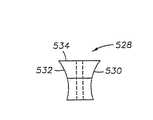
また、図18は、チャンバ壁部に形成されたクリーニングガス送出チャネルを示している。ガスは、遠隔源500からチャンバの後壁部520に向かって水平方向に配設された第1のガスチャネル28に送出される。第1のガスチャネル28は後壁部の長さだけ延び、チャンバの対置する両側部にガスを送出するようにしている。チャンバの下部部分には中央ガス522接続部が形成され、送出導管510の第1のガスチャネル28に接続されるようにしている。また、チャンバの各側壁部には第2のガスチャネル524が形成され、チャンバ内のスリット開口部526で終端されている。チャネルが形成されているコーナーカバーが作られて、第1のガスチャネル28の端部を、側壁部に形成された側部のガスチャネル524に接続するようにしている。好適には、コーナーカバーはチャンバ本体の所定の位置に溶接されて、チャンバ本体を介してチャンバのスリット開口部526にガスが送出されることを促進するようにしている。
【0096】
第2のガスチャネル524のスリット開口部526内には、第1のガス拡散部材528が配設されて、クリーニングガスがチャンバに導かれるようになる。図19は、チャンバの対置する両側部にクリーニングガスを送出する湾曲側面部530,532を示すガス拡散部材528の平面図である。湾曲した表面530,532は第2のガスチャネル524の両側に配置され、外側にチャンバ内に向かってガスを導くようにしている。
【0097】
図20は、ガス拡散部材528の側面図である。ガスディフューザの後部534は傾斜の付いた状態になって、チャネル524内に配設されたガスディフューザを越えてガスが通過し、チャンバの両側部にガスが導かれるようになることを可能にしている。ガス拡散部材の一端部には凹部536が形成されて、ガスチャネル内の所定位置でディフューザの係合を楔式でしている。凹部と結合するために、楔部538が設けられ、ねじにより楔部を凹所内の所定位置に押し込み、楔部をディフューザに接続し、また、ディフューザをチャンバ本体に接続する。
【0098】
他の実施形態では、チャンバ内において、チャンバの各スリット開口部526に近接してガスバフラ(gas baffler)を配設し、クリーニングガスを上向きの方向に、また、プロセスキットやESC104の上部に向かわせてもよい。図21は、フランジ542によりディフューザ528に取り付けられているバフラ540の斜視図が示されている。バフラの本体544には湾曲した表面546が設けられ、チャンバ内に配置されているときは、わずかに上向きに傾斜し、クリーニングガスをチャンバ内で上向きの方向に、また、ESC104やプロセスキットの上部に向かわせるようにしている。
【0099】
クリーニングガスが上記ESC及びプロセスキットの上からチャンバ内に送り込まれると、クリーニング工程が最も効果的なものになることが明らかになっている。さらに、チャンバ内で上向きに、また、ESC及びプロセスキットから離れる方向にガスが流れて、クリーニング工程中に遊離される粒子や残留物を、クリーニングガスがESCに押しつけることが防止されるようにすることが好ましい。粒子がESC上に残ったままであるならば、チャックでの固定中に、ヘリウムの漏れが生じるおそれが増大する。バッフル(baffle)はガス流を上向きにそらせて、クリーニングを向上させ、ESC上への粒子の堆積を防止するようにしている。
【0100】
上記は本発明の好適な実施形態にしたがったものであるが、本発明のその他の実施形態もその基本的な範囲から逸脱することなく創案してもよく、また、本発明の範囲は、上記の特許請求の範囲に記載する請求項にしたがって決定される。
【図面の簡単な説明】
【図1】 本発明の処理チャンバの断面図である。
【図2】図2(a)〜図2(c)は、本発明が進歩するために使用することができる種々のRF整合の構成を示す電気的な概略図である。
【図3】本発明の2重領域RFプラズマ源を示す概略断面図である。
【図4】上部温度制御アセンブリ及び上部アンテナの拡大図である。
【図5】本発明の基板支持部材の断面図である。
【図6】本発明の基板支持部材の断面平面図である。
【図7】基板支持部材を配設しているチャンバの断面平面図である。
【図8】静電チャックの一の実施形態の平面図である。
【図8a】静電チャックの他の実施形態の平面図である。
【図9】図8の静電チャックの一実施形態の断面図である。
【図10】図8及び図9の静電チャックの温度制御の態様の系統線図である。
【図11】静電チャック及びカバーリングの断面図である。
【図12】ソースコイルに近接して配設されているカバーリングの断面図である。
【図13】本発明のガス制御装置を示す部分的に断面になった側面図である。
【図14】ガス分配リング及び第1のガスチャネルを示す部分的に断面になった側面図である。
【図15】ガス分配リング及び第2のガスチャネルを示す部分的に断面になった側面図である。
【図16】中央ガス供給アセンブリを示す部分的に断面になった側面図である。
【図17】リッドアセンブリのガス分配リング及びルーズプレートの拡大図である。
【図18】マイクロ波遠隔プラズマクリーニング部及びチャンバに対するその位置を示す部分的に断面になった概略側面図である。
【図19】ガスディフューザの平面図である。
【図20】ガスディフューザの側面図である。
【図21】ガスバフラの斜視図である。
【符号の説明】
10…処理装置、12…チャンバ本体、14…リッドアセンブリ、16…基板支持部材、20…環状処理領域、22…排気通路、24…基板入口ポート、26…側方入口ポート、28…ガスチャネル、30…遠隔プラズマ源、32…ドーム、33…ベースプレート、44…スリットバルブ、46…フランジ、50…外壁部、51…片持ち壁部、52…チャンバ内壁部、54…排気ポート、56…ツインブレードスロットルアセンブリ、58…ゲートバルブ、60…ターボ分子ポンプ、62…エネルギ送出アセンブリ、64…温度制御アセンブリ、66…側壁部、68…最上部、70…接合部、72…最上部コイル、74…側部コイル、76,78…電源、80…加熱プレート、82…冷却プレート、84…薄層、86…熱伝導性プレート、88…第2の層、90…第3の層、94,96…絶縁スリーブ、98…ESC収容部分、99…基板収容表面、100…パイロット、102…絶縁部材、104…静電チャック(ESC)、108…凹部、110…基板位置決めアセンブリ、112…底部プレート、114,118…通路、116…支持腕部、120…基板リフトアセンブリ、122…基板支持ピン、123…取り付けプレート、126…エレベータ機構、128…シャフト、130…取り付けプレート、132…スリーブ、134…穴部、140…取水部、142…排水部、144,146…冷却チャネル、148…給水マニホールド、164…静電チャック、166…突起部、168…中央領域、170…周縁領域、172…内側シール部、174…外側シール部、176…リング、178…内側リング、180…真空穴部、182…ウェハ、184…電極部分、186…誘電体、190…側部、194…周縁部分、196…温度センサ、198…定数、200…基板収容面、202,204,206,208,212,214…ブロック、210…ウェハの温度、211…フィードバック線、213…帰還信号、230…基板サポートアセンブリ、232…支持体、234…フランジ、236…誘電体層、238…上面、240…リフトピン穴、242…シールド、244…導電材料、246…カラー、248…カバー、250…間隙、252…第2の間隙、256…上面、260…ソースRFコイル、300…ガス分配アセンブリ、302,304,306…ガスノズル、308…ガス通路、310…ガス分配リング、312…中央ガス供給部、314…ポート、316,318…ガスチャネル、320…チャネル、322,324…Oリング、326…テフロンシール、328…凹部、332…通路、334…ベース、336,338…Oリング、340…ポート、342…ガス通路、350…チャネル、500…遠隔プラズマ源、502…チャンバ、506…ガス出口部、508…アプリケータ管、510…送出式水冷送出導管、512…導波管、520…後壁部、522…中央ガス、524…第2のガスチャネル、526…スリット開口部、528…第1のガス拡散部材、530,532…湾曲側面部、534…後部、536…凹部、538…楔部、540…バフラ、542…フランジ、544…本体、546…湾曲面、W…ウェハ。[0001]
Field of the Invention
The present invention relates to an apparatus and method for processing a semiconductor substrate, and more particularly to a thin film on a substrate, preferably αC, αFC, SiN, SiON, doped SiO.2 , Undoped SiO2 And a high density plasma (HDP) chemical vapor deposition (CVD) apparatus for depositing BiN thin films.
[0002]
[Prior art]
Plasma devices used for semiconductor processing such as chemical vapor deposition (CVD), etching, reactive ion etching, etc. typically use either inductive coupling or capacitive coupling to ignite and maintain the plasma. is there. An advantage of inductively coupled plasma over capacitively coupled plasma is that inductively coupled plasma is generated with a much lower bias voltage applied to the substrate, thus reducing the possibility of damaging the substrate. In addition, inductively coupled plasmas operate at much lower pressures than capacitively coupled plasmas, but have higher ion densities, thereby resulting in higher deposition rates and longer mean free paths. These advantages result in in situ sputtering and / or ion directionality during processing.
[0003]
More recently, a high density plasma (HDP) CVD process has been used to combine chemical reactions with physical sputtering. In the HDP-CVD process, radio frequency (RF) energy is applied to a reaction region in the vicinity of the substrate surface to promote dissociation of the reaction gas and generate a plasma of highly reactive ion species. In addition, the relatively inert ion component, Ar, has a high momentum (electric field) used to selectively remove the deposited thin film material from a specific region along the cross-sectional shape of the thin film based on the sputtering rate curve. Given. The high reactivity of the released ionic species reduces the energy required for the chemical reaction to occur, thus lowering the temperature required for these processes.
[0004]
The goal of most HDP-CVD processes is to deposit a thin film of uniform thickness across the surface of the substrate, while at the same time filling the proper gap between the electrical lines formed on the substrate and other features. Is also to do. Uniformity of deposition and gap / via embedding are the structure of the power supply, the change in gas flow rate, the output of the high frequency generation power supply, the output of the bias high frequency generation power supply, the symmetry of the nozzle distribution, the number of nozzles, It is very sensitive to the design of the gas nozzle, including the height of the nozzle disposed over the substrate support and the lateral position of the nozzle relative to the substrate support. When the process and processing gas performed inside the apparatus change, these variables also change.
[0005]
One of the problems faced during semiconductor manufacturing is the generation and maintenance of a uniform density plasma on the substrate. The uniformity of the plasma depends not only on the flow rate of gas flowing into and out of the device, but also on the magnetic and electric fields generated in the device. As the size of the substrate increases, i.e. up to 300 mm, it becomes more difficult to achieve uniformity across a larger area.
[0006]
Another problem that affects deposition uniformity is uneven gas distribution across the substrate surface. Generally, a gas plenum is provided at the peripheral edge of the processing region, and a plurality of nozzles extend radially inward to supply gas to the substrate surface. In some applications, gas tends to be distributed unevenly across the substrate surface, resulting in more gas towards the edge of the substrate and less gas towards the center of the substrate. In addition, the reaction gas is typically mixed in a gas injector prior to introduction into the chamber. In such a case, material tends to accumulate within the gas injector itself, thereby causing some gas injectors to become clogged and further increase the uneven gas distribution.
[0007]
Furthermore, another problem is that the temperature of the entire substrate surface is kept uniform. When processing a substrate, there is a significant thermal load because the substrate surface is exposed to plasma radiation and ion bombardment. If there is a temperature gradient on the surface of the substrate, thin film deposition may proceed unevenly. Therefore, it is important to accurately control the temperature of the substrate.
[0008]
Another problem is the deposition of material on the device itself. During processing, deposition material is deposited throughout the chamber, such as the substrate support member and gas distribution components. Over time, the material deposits described above will flake and fall into the chamber, resulting in substrate particulate contaminants that compromise the integrity of the device being fabricated. Therefore, the device must be cleaned periodically. A preferred cleaning method is to introduce a cleaning gas into the chamber and react with the deposited material to form a product that can be discharged from the chamber. Typically, when a cleaning gas such as fluorinated gas is introduced into the chamber, the plasma is ignited in the chamber. The resulting excited product reacts with the deposited material, creating a gas phase byproduct and then evacuating the chamber. One problem with such processes is that cleaning is typically localized only to regions adjacent to the plasma. In order to improve the cleaning of the entire surface of the exposed chamber, the time for performing the cleaning process is increased, but for this reason, the throughput is decreased and / or the cleaning process is performed using a high temperature. Some chamber surfaces are effectively over-cleaned, increasing the cost of consumable parts and / or maintenance intervals.
[0009]
Accordingly, there is a need for a manufacturing apparatus that increases the uniformity of conditions for forming a CVD thin film on a substrate, including enhancement of the cleaning function and improvement of throughput, in a manner that increases manufacturing value.
[0010]
SUMMARY OF THE INVENTION
In an embodiment of the present invention, an HDP-CDV device is provided that uses doped and undoped silicon dioxide deposition and sputtering and has an aspect ratio of greater than 1.2: 1 and less than 0.5 microns. It enables excellent gap filling and blanket film deposition for wafers with specific dimensions. The apparatus of the present invention consists of a dual RF domain inductively coupled plasma source, a dual domain gas distributor, temperature controlled chamber components, a chamber body evacuated by a symmetrical turbomolecular pump, a double cooling domain electrostatic Includes a chuck, an all-ceramic / aluminum alloy chamber structure, and a plasma chamber cleaning remote.
[0011]
[Description of Preferred Embodiment]
So that the manner in which the above features, advantages and objects of the present invention can be understood in detail, a more detailed description of the invention summarized above may be had by reference to the embodiments illustrated in the accompanying drawings. Do it.
[0012]
However, the attached drawings are only basic embodiments of the present invention, and therefore should not be regarded as limiting the scope of the present invention, and may lead to other embodiments having equivalent operational effects. It should be noted.
[0013]
The apparatus of the present invention is described in detail below with reference to the following subassemblies: chamber body, chamber lid assembly, cathode and lift assembly, process kit, gas distribution assembly and remote plasma source. .
[0014]
Chamber body
FIG. 1 is a cross-sectional view of a
[0015]
Preferably, the
[0016]
The upper surface of the
[0017]
The
[0018]
A pumping stack including a twin
[0019]
During processing of the substrate in the chamber, the vacuum pump evacuates the chamber,0.533-0.800Pa (4-6mTorr)And a metered process gas or gas flow rate is fed into the chamber through the gas distribution assembly. The chamber pressure is controlled by directly measuring the chamber pressure and sending this information to a controller that opens and closes a valve to adjust the pumping speed. The gas flow rate / concentration is directly controlled by the mass flow controller via software settings provided in the process recipe. In addition, by measuring the flow rate of the gas exhausted out of the chamber through the
[0020]
Chamber lid assembly
Basically, the chamber lid assembly 34 consists of an
[0021]
Basically, the
[0022]
Two independently powered RF coils, the
[0023]
Each power supply includes a control circuit that measures the reflected power and adjusts the digitally controlled synthesizer in the RF generator, essentially starting to sweep the frequency from 1.8 MHz to minimize the reflected power. ing. When the plasma ignites, the circuit changes as the plasma acts as a resistor in parallel with the coil. At this stage, the RF generator continues to sweep the frequency until the minimum reflected power point is reached again. The power circuit is designed so that each set of windings resonates at or near the frequency at which the minimum reflected power point is achieved, so that the winding voltage is high enough to maintain the plasma. Sufficient current can flow. Thus, frequency tuning ensures that the device is maintained near the resonant frequency if the resonant point of the circuit changes during processing. Thus, frequency tuning eliminates the need for impedance matching and circuit tuning by changing the value of impedance matching components (eg, capacitors and inductors).
[0024]
Each power supply ensures that the desired power is delivered to the load despite the impedance mismatch, even if the impedance mismatch continuously changes due to changes in plasma impedance. In order to ensure that power is delivered accurately to the load, each RF generator disperses the reflected power itself to increase the output power, so that the delivered power remains at the desired level. It becomes like this.
[0025]
2 (a), 2 (b) and 2 (c) schematically show the configurations of three independent local RF matching sections. FIG. 2A shows a configuration of a matching unit in which one end of the coil L is grounded. The two capacitors C1 and C2 form an RF voltage divider. In FIG. 2B, the load (plasma) frequency is matched by using a balanced coil L in which two shunt capacitors C2 and C3 at both ends are grounded. Finally, in FIG. 2C, a Pi (B) matching network in which two variable capacitors at both ends of the coil L are grounded is used. Since the output impedance of most conventional RF generators is designed to be 50Ω, using the matching network 2 (a), (b) or (c), the lower limit is from 5Ω to the upper limit is 900Ω. Maximum power can be transmitted to the plasma in the impedance range (in the case of balanced load). With such a double coil device, the ion density profile in the radial direction can be controlled in the reactor chamber.
[0026]
FIG. 3 is a schematic side view of the chamber mainly showing the shape and dimensions of the coils and the RF power feeding portions of the
[0027]
The
[0028]
The cooling
[0029]
[0030]
By direct conduction, the
[0031]
Cathode and lift assembly
Next, the cathode and lift assembly will be described with reference to FIGS. The substrate support member includes an element that can be disposed inside the chamber and an element that can be disposed outside the chamber. The elements of the
[0032]
The
[0033]
Further, the
[0034]
FIG. 7 is a cross-sectional plan view showing the
[0035]
Furthermore, in order to further minimize the effect on the gas near the substrate surface caused by fluid blockage, restriction or obstruction when the fluid passes inside and near the cantilever arm, the
[0036]
The
[0037]
The
[0038]
Next, the operation will be described. The substrate is placed on the
[0039]
After the processing, the elevator mechanism raises the support pins 122 to lift the substrate and separate it from the
[0040]
During processing, the plasma in the CVD processing environment generates a large amount of heat, but the total heat generated by the plasma depends at least in part on the power density of the plasma. Since some of this heat is transferred to the substrate, it must be removed from the substrate in order to maintain the substrate temperature below a predetermined critical temperature. In order to remove such heat, the
[0041]
FIG. 8 is a plan view of one embodiment of an
[0042]
Helium gas is inserted into the
[0043]
The
[0044]
Next, the operation will be described. To heat the wafer, low pressure helium (133-2000Pa (1-15 torr)) To the
[0045]
In some embodiments, the seal is made of the same ceramic coating as the rest of the
[0046]
A preferred heat transfer gas is helium because it is inert and relatively inexpensive. Or argon, oxygen, CFFourAlternatively, other gas may be used, or a mixed gas may be used. For example, a mixture may be used to provide additional pressure control capabilities. A specific gas can be selected to be compatible with the chemical treatment in the chamber and the leaked gas can have a minimal effect on the chemical reaction. For example, in an etching reaction using fluorine as an etching species, CF as the backside heat transfer gasFourIt is desirable to use
[0047]
Since heat transfer occurs primarily through helium gas, it is desirable to minimize the seal area and the size and number of protrusions for such purposes. Therefore, the contact area in the area of the substrate needs to be smaller than the non-contact area. On the other hand, the seal portion is required to prevent gas leakage, and the protrusions must have a sufficient size and spacing to mechanically support the wafer. In addition, there are other factors that should be optimized. The height of the protrusions that determine the gap between the substrate and the substrate support between the protrusions allows the gas to be quickly distributed over the entire area without affecting the processing start time. It must be sufficient. Basically, this should be approximately a few seconds, and preferably the gas is dispensed in less than 10 seconds.
[0048]
In order for heat transfer to be optimal, the gap is small enough that the heat transfer is mainly performed by molecules that move directly from the substrate to the substrate support without colliding with other gas molecules, and free molecule heat transfer. There is a need. Therefore, the gap needs to be smaller than the average free path of gas (the average value of the free path when a mixed gas is used). The mean free path is a function of the gas pressure and the molecular collision cross section. Using various pressures, the mean free path changes. In a preferred embodiment, the maximum pressure applied mean free path is used to determine the size of the gap.
[0049]
In addition, it is necessary to reduce the ratio of the gap to the total thickness of the dielectric to avoid local substrate anomalies. If this ratio becomes significant, the equivalent capacitance between the space and the protrusion changes significantly, and a considerably different electric field is applied to the substrate. Thus, different electric fields can adversely affect chemical processing and cause non-uniformities in thin films that are deposited, etched, doped, or undergo other attribute changes. There are always some differences, but it is desirable to keep them to a minimum.
[0050]
In addition, the significance of this ratio differs depending on the dielectric material, and in particular, the difference (basically the same) between the dielectric constants of the material and the heat transfer gas. The closer the two dielectric constants, the less important the gap is.
[0051]
Another important point in setting the gap size is to avoid generating a plasma by the heat transfer gas between the substrate support and the backside of the wafer. This is believed to begin to become important when the gap size is several times the mean free path of the heat transfer gas.
[0052]
For one embodiment of an electrostatic chuck, the thickness of the ceramic coating is approximatelyAbout 0.178-0.254mm (About 7-10 mil)It has become. If you used KaptonJ,0.025-0.051mm (1-2 mil)The thickness of can be used. In order to achieve the purpose of the chuck, the dielectric should ideally be as thin as possible while maintaining manufacturing consistency and avoiding dielectric breakdown. The mean free path of helium at the two region pressures mentioned above isAbout 0.025 to 0.127 mm (About 1-5 mil)(At very high pressures, the mean free path can be smaller). Therefore,0.017-0.030mm (0.7-1.2mil)The heights of the protrusions were selected and tested and found to be effective. This provides a gap that is smaller than the mean free path of helium at the desired pressure. Preferably, the gap is no more than twice the mean free path of the heat transfer gas at a reasonable pressure, and more preferably no more than the mean free path.
[0053]
The spacing between the protrusions is as large as possible as long as the substrate is supported without bending. In one embodiment, the substrate is kept flat, while in other embodiments, the height of the protrusion or the top surface of the substrate support is changed (the height of the protrusion is equal) and curved. It is desirable to properly support the substrate. Another factor is to avoid sharp points that cause local anomalies in the electric field. If the interval is large, the movement of charges when the chuck is released is also affected, which may cause damage.
[0054]
The optimal center distance of the protrusion is2.54-7.62mm (100-300 mil)And preferablyApproximately 7.62mm (About 300 mil)It is clear that Preferably, the size of the protrusion itself is a diameter.0.254 to 3.81 mm (10-150 mil)More preferably3.30mm (130 mil)It has become. Although rectangular protrusions are shown, they are simply because they are easy to manufacture, and other shapes can be used as well. For example, an annular thing can be used.
[0055]
In the illustrated embodiment, an opening for removing gas is not shown in the outer peripheral region, but in other embodiments it may be provided. The helium pressure can be controlled by using high or low pressure helium or by evacuating with a vacuum pump. Similarly, for the central region, the pressure can be controlled by either or a combination of both of these methods. By placing the helium source as a ring close to the edge in combination with a vacuum close to the center of the support, an additional pressure gradient is created in the central region and decreases towards the center. For example, other embodiments of the present invention perform coarse tuning of heat transfer through two pressure zones by this method and fine tuning by placing a helium inlet and a vacuum outlet in the central zone. In other embodiments, more fine-tuning can be done using two or more regions, at the expense of requiring more hardware.
[0056]
FIG. 9 is a side view of one embodiment of the
[0057]
The thinner the dielectric at the
[0058]
In other embodiments, varying thicknesses of dielectric can be used without two pressure regions or without protrusions. The change in the dielectric coating may be continuous or stepped. The difference from the staircase format makes manufacturing easier and less expensive.
[0059]
Another advantage with respect to the
[0060]
As shown in FIG. 9, a
[0061]
FIG. 10 is a signal system diagram of a feedback control apparatus illustrating temperature control. The diagram of FIG. 10 is for a closed loop temperature controller for controlling the pressure of helium. Alternatively, an open loop device without a temperature sensor may be used. Prior experimentation can represent an appropriate helium pressure for the desired process parameters, and thus, in other embodiments, the temperature sensor can be eliminated. FIG. 9 includes both functions executed in the processor and physical effects.
[0062]
The temperature set value is provided as an input of a user program from the control program in the memory 245 to the control device. The temperature set value is multiplied by a constant 198 by the controller, and the result is added to the
[0063]
[0064]
The function executed by the control device is performed by controlling the program in the memory 245. The program includes instructions for performing various steps, such as instructions for reading a temperature indication from a temperature sensor, instructions for comparing the temperature with a desired input set temperature, and a pressure valve (or flow rate). And a command for changing the gas pressure to a specific pressure range by controlling the suppression device. In the event of a failure or the like, another command for shutting off the gas is defined.
[0065]
The helium pressure can be controlled by increasing or decreasing the pressure when using one simple pressure electrostatic chuck. Alternatively, when using two pressure zones as in the preferred embodiment of the present invention, the outer and inner helium pressures can be controlled independently. For example, the temperature of each region can be inferred from a single temperature sensor located near the intersection of the two regions. Alternatively, two different temperature sensors can be used. In other embodiments, the temperature sensor may be attached to the top surface of the electrostatic chuck or may be in direct contact with the wafer itself. For example, if there is a leak between regions that causes pressure fluctuations, a temperature sensor may be used to estimate the pressure. Basically, some distance away from the wafer, the pressure regulator detects only the pressure at its output, which may have a different pressure below it. The temperature sensor can be used to infer the actual pressure under the wafer. Depending on the roughness of the wafer surface, the amount of leakage may vary, and the pressure supplied may need to be varied.
[0066]
It is fundamental that the control device has certain restrictions on it. For example, the pressure of helium is limited so that the wafer is not lifted away from the electrostatic chuck, or so that a thermal gradient is created where the pressure differential increases and the wafer breaks due to thermal stress. If any of the above limits are exceeded or some other fault occurs, the gas flow stops.
[0067]
Process kit
The process kit consists of a collar and a cover. In addition, a skirt may be used. The color of the ceramic varies depending on the size and type of the wafer, and is disposed between the electrostatic chuck and the quartz cover. The main purpose of the collar is to protect the electrostatic chuck flange from the effects of plasma. The cover extends from the collar to the outer peripheral edge of the cathode assembly, and its main purpose is to protect the cathode assembly from the effects of plasma. The skirt may be disposed in the lower chamber to protect the spacers and O-rings that seal the upper and lower chambers from the effects of plasma.
[0068]
In one aspect, the present invention provides an improved process kit or shield for an electrostatic chuck of a semiconductor processing chamber that prevents or resists the deposition of gas products. In addition, the shield removes oxide deposits at high speed, resulting in increased throughput in the wafer manufacturing process.
[0069]
In one embodiment, the collar or cover may include one or more surfaces or conductive material disposed on the interior to enhance cleaning of the surfaces. In general, an inductive coil disposed around a
[0070]
As an example, metal can be deposited on one surface of a process kit component, such as a collar or cover, to provide a conductor capable of inducing current. The operation of the heat treatment is similar to that seen in a transformer with the coil as the external winding and the metal layer as the internal winding.
[0071]
FIG. 11 is a cross-sectional view of the electrostatic chuck and the process kit.
[0072]
Referring to FIG. 11, the
[0073]
In one embodiment, the
[0074]
As shown in FIG. 11, the
[0075]
The
[0076]
During the deposition process, oxide from the process gas deposits on a substantial portion of the wafer W and the exposed surface of the chamber, such as the inner wall of the enclosure and the
[0077]
As shown in FIG. 11, when the wafer is on or adjacent to the top surface of the
[0078]
Referring to FIG. 12, which is a cross-sectional view of the process chamber process kit, an inductive HDP source
[0079]
In the case of the circular shape shown in FIG. 12, the resistance R is approximately 2BrD / W @ d. Here, r is the size in the radial direction of the outer diameter of the thin annular body of the conductive material, w is the width of the conductive material, d is the thickness of the conductive material, and D is the resistivity of the conductive material. The resistance R is preferably controlled by changing w @ d, that is, the cross-sectional area of the
[0080]
In another aspect of the present invention, the cleaning rate or deposition removal rate of the process kit is basically a function of temperature (ie, the higher the shielding during processing, the faster it can be cleaned). is there. During cleaning, the
[0081]
Gas distribution assembly
Hereinafter, the
[0082]
Hereinafter, the gas distribution ring and the gas manifold arranged at the center will be described.
[0083]
Basically, the
[0084]
FIG. 14 is a cross-sectional view showing a
[0085]
The
[0086]
FIG. 15 is a cross-sectional view showing the
[0087]
One advantage of the present invention is that it facilitates the gas distribution ring when the ring forms a port to accommodate and position the nozzle tip at various angles so that the gas distribution pattern can be adjusted. It can be removed and replaced. In other words, in some applications, it is advantageous to form ports in the ring and direct some of the gas nozzles upward in the chamber, or conversely some of them downward in the chamber. It has become. The port formed in the gas distribution ring is machined so that the desired angle can be selected to provide the desired processing result. Furthermore, if there are at least two gas channels through which at least two gases can be separately pumped into the chamber, it will be possible to have outstanding control over the reactions that occur between the various gases. Furthermore, by separately pumping the gas into the chamber, reaction of the gas in the gas distribution assembly can be prevented.
[0088]
FIG. 16 is a cross-sectional view showing the central
[0089]
FIG. 17 is an enlarged view showing the
[0090]
The first gas source 352 and the first gas control device 354 control the first gas entering the
[0091]
A third gas source 364 and a third gas control device 366 supply a third gas via line 368 to a gas channel located at the top of the chamber. The fourth gas source 370 and the fourth gas control device 372 supply the fourth gas to the
[0092]
Remote plasma cleaning device
A remote plasma source includes a remote chamber having a gas inlet and a gas outlet, a power source coupled to the chamber by a waveguide, and an applicator disposed between the gas inlet and the gas outlet in the chamber It is fundamental to have an applicator tube. FIG. 18 shows a schematic diagram of a
[0093]
Preferably, power in the range of 2000 to 5000 W is supplied to the
[0094]
In the chamber, the cleaning reaction that proceeds at a very high speed has the following form:
4F*(Gas)+ SiOThree6SiF4 (Gas)+ O2 (Gas)
And 2F*(Gas)+ SiO2 (Gas)6SiF2 (Gas)+ O2 (Gas)
And is thought to produce a gaseous product that is removed from the chamber 13 by evacuating the gas phase. Long-excitation neutral fluorine species F*The most effective reaction gas for generating a high concentration of NFThree, F2, SF6, ClFThreeAnd C2F6It is. However, other cleaning gases that can be excited by microwaves and react with the deposited material in the chamber may be used. In the case of the remote microwave cleaning device of the present invention shown in FIG.ThreeAnd F2Is preferably diluted with an inert argon gas to a concentration of 10 to 50%. The desired cleaning reaction resulting from the use of a remote plasma source proceeds without ion bombardment of the chamber or substrate support structure, avoiding the need for periodic replacement of the wafer cover on the
[0095]
FIG. 18 shows a cleaning gas delivery channel formed in the chamber wall. Gas is delivered from a
[0096]
A first
[0097]
FIG. 20 is a side view of the
[0098]
In other embodiments, a gas baffler is provided in the chamber adjacent to each slit opening 526 in the chamber to direct the cleaning gas upward and to the top of the process kit or
[0099]
It has been found that the cleaning process is most effective when cleaning gas is pumped into the chamber from above the ESC and process kit. In addition, the gas flows upwards in the chamber and away from the ESC and process kit to prevent the cleaning gas from pressing the ESC against particles and residues released during the cleaning process. It is preferable. If the particles remain on the ESC, there is an increased risk of helium leakage during clamping with the chuck. The baffle deflects the gas flow upward to improve cleaning and prevent particle buildup on the ESC.
[0100]
While the above is in accordance with a preferred embodiment of the present invention, other embodiments of the invention may be devised without departing from the basic scope thereof, and the scope of the invention is In accordance with the claims set forth in the following claims.
[Brief description of the drawings]
FIG. 1 is a cross-sectional view of a processing chamber of the present invention.
FIGS. 2 (a) -2 (c) are electrical schematics showing various RF matching configurations that can be used to advance the present invention.
FIG. 3 is a schematic cross-sectional view showing a dual region RF plasma source of the present invention.
FIG. 4 is an enlarged view of the upper temperature control assembly and the upper antenna.
FIG. 5 is a cross-sectional view of a substrate support member of the present invention.
FIG. 6 is a cross-sectional plan view of a substrate support member of the present invention.
FIG. 7 is a cross-sectional plan view of a chamber in which a substrate support member is disposed.
FIG. 8 is a plan view of one embodiment of an electrostatic chuck.
FIG. 8a is a plan view of another embodiment of an electrostatic chuck.
9 is a cross-sectional view of one embodiment of the electrostatic chuck of FIG.
10 is a system diagram of a temperature control mode of the electrostatic chuck of FIGS. 8 and 9. FIG.
FIG. 11 is a cross-sectional view of an electrostatic chuck and a cover ring.
FIG. 12 is a cross-sectional view of the cover ring disposed in the vicinity of the source coil.
FIG. 13 is a partially sectional side view showing the gas control apparatus of the present invention.
FIG. 14 is a partially sectional side view showing a gas distribution ring and a first gas channel.
FIG. 15 is a partially cross-sectional side view showing a gas distribution ring and a second gas channel.
FIG. 16 is a partially cross-sectional side view showing a central gas supply assembly.
FIG. 17 is an enlarged view of the gas distribution ring and loose plate of the lid assembly.
FIG. 18 is a schematic side view, partially in section, showing the microwave remote plasma cleaning section and its position relative to the chamber.
FIG. 19 is a plan view of a gas diffuser.
FIG. 20 is a side view of a gas diffuser.
FIG. 21 is a perspective view of a gas baffle.
[Explanation of symbols]
DESCRIPTION OF
Claims (9)
Translated fromJapanese(ii)前記側壁部の一方の端部に配設されたリッドと、
(iii)前記側壁部の反対側の端部に配設された底部と、
を有するチャンバ、
(b)前記側壁部に片持ち式で取り付けられた基板支持部材、
(c)前記リッドを通って配設され、第1の処理ガスを前記チャンバ内に入れるようにする第1の処理ガス入口部、
(d)前記側壁部を通って配設され、第2の処理ガスを前記チャンバ内に入れるようにする第2の処理ガス入口部、
(e)前記チャンバの前記底部に配設された排気ポート、
(f)前記リッドに近接して配設されたアンテナ、
(g)前記アンテナに接続された可変周波数RF源、及び、
(h)前記可変周波数RF源に接続され、前記アンテナへの電力伝送の変化に応じて前記可変周波数RF源の出力を連続的に調整するようにする制御回路、
を備え、
(i)前記制御回路が反射電力を測定し、前記可変周波数RF源のシンセサイザを調整することで周波数を掃引して反射電力を最小にする、基板を処理するための装置。(A) (i) side wall,
(Ii) a lid disposed at one end of the side wall;
(Iii) a bottom portion disposed at an end opposite to the side wall portion;
A chamber having
(B) a substrate support member attached to the side wall portion in a cantilever manner;
(C) a first process gas inlet disposed through the lid for allowing a first process gas to enter the chamber;
(D) a second processing gas inlet portion disposed through the side wall portion for allowing a second processing gas to enter the chamber;
(E) an exhaust port disposed at the bottom of the chamber;
(F) an antenna disposed in proximity to the lid;
(G) a variable frequency RF source connected to the antenna; and
(H) a control circuit connected to the variable frequency RF source and configured to continuously adjust the output of the variable frequency RF source in response to a change in power transmission to the antenna;
With
(I) An apparatus for processing a substrate, wherein the control circuit measures reflected power and adjusts the synthesizer of thevariable frequency RF sourceto sweep the frequency to minimize reflected power .
Applications Claiming Priority (2)
| Application Number | Priority Date | Filing Date | Title |
|---|---|---|---|
| US08/679,927US6170428B1 (en) | 1996-07-15 | 1996-07-15 | Symmetric tunable inductively coupled HDP-CVD reactor |
| US08/679927 | 1996-07-15 |
Related Child Applications (1)
| Application Number | Title | Priority Date | Filing Date |
|---|---|---|---|
| JP2007293616ADivisionJP2008091938A (en) | 1996-07-15 | 2007-11-12 | Process kit, wafer processing apparatus, and process kit heating method |
Publications (2)
| Publication Number | Publication Date |
|---|---|
| JPH10116826A JPH10116826A (en) | 1998-05-06 |
| JP4688983B2true JP4688983B2 (en) | 2011-05-25 |
Family
ID=24728963
Family Applications (2)
| Application Number | Title | Priority Date | Filing Date |
|---|---|---|---|
| JP22293297AExpired - Fee RelatedJP4688983B2 (en) | 1996-07-15 | 1997-07-15 | Inductively coupled HDP-CVD reactor |
| JP2007293616APendingJP2008091938A (en) | 1996-07-15 | 2007-11-12 | Process kit, wafer processing apparatus, and process kit heating method |
Family Applications After (1)
| Application Number | Title | Priority Date | Filing Date |
|---|---|---|---|
| JP2007293616APendingJP2008091938A (en) | 1996-07-15 | 2007-11-12 | Process kit, wafer processing apparatus, and process kit heating method |
Country Status (6)
| Country | Link |
|---|---|
| US (2) | US6170428B1 (en) |
| EP (1) | EP0819780B1 (en) |
| JP (2) | JP4688983B2 (en) |
| KR (1) | KR100268158B1 (en) |
| DE (1) | DE69727624T2 (en) |
| TW (1) | TW363212B (en) |
Families Citing this family (330)
| Publication number | Priority date | Publication date | Assignee | Title |
|---|---|---|---|---|
| US6070551A (en)* | 1996-05-13 | 2000-06-06 | Applied Materials, Inc. | Deposition chamber and method for depositing low dielectric constant films |
| US6170428B1 (en)* | 1996-07-15 | 2001-01-09 | Applied Materials, Inc. | Symmetric tunable inductively coupled HDP-CVD reactor |
| US6184158B1 (en)* | 1996-12-23 | 2001-02-06 | Lam Research Corporation | Inductively coupled plasma CVD |
| US6749717B1 (en) | 1997-02-04 | 2004-06-15 | Micron Technology, Inc. | Device for in-situ cleaning of an inductively-coupled plasma chambers |
| US6286451B1 (en)* | 1997-05-29 | 2001-09-11 | Applied Materials, Inc. | Dome: shape and temperature controlled surfaces |
| US6797188B1 (en)* | 1997-11-12 | 2004-09-28 | Meihua Shen | Self-cleaning process for etching silicon-containing material |
| EP0926716B1 (en)* | 1997-12-17 | 2003-07-16 | Tokyo Electron Limited | Method of processing a semiconductor substrate |
| US6194038B1 (en)* | 1998-03-20 | 2001-02-27 | Applied Materials, Inc. | Method for deposition of a conformal layer on a substrate |
| WO1999054521A2 (en)* | 1998-04-21 | 1999-10-28 | Applied Materials, Inc. | Method and apparatus for modifying the profile of high-aspect-ratio gaps using differential plasma power |
| US6200911B1 (en) | 1998-04-21 | 2001-03-13 | Applied Materials, Inc. | Method and apparatus for modifying the profile of narrow, high-aspect-ratio gaps using differential plasma power |
| KR100296137B1 (en)* | 1998-06-16 | 2001-08-07 | 박종섭 | method for fabricating semiconductor device having HDP-CVD oxide layer as passivation layer |
| US6230651B1 (en) | 1998-12-30 | 2001-05-15 | Lam Research Corporation | Gas injection system for plasma processing |
| US6374831B1 (en)* | 1999-02-04 | 2002-04-23 | Applied Materials, Inc. | Accelerated plasma clean |
| US6367413B1 (en) | 1999-06-15 | 2002-04-09 | Tokyo Electron Limited | Apparatus for monitoring substrate biasing during plasma processing of a substrate |
| US6395095B1 (en) | 1999-06-15 | 2002-05-28 | Tokyo Electron Limited | Process apparatus and method for improved plasma processing of a substrate |
| US6431112B1 (en) | 1999-06-15 | 2002-08-13 | Tokyo Electron Limited | Apparatus and method for plasma processing of a substrate utilizing an electrostatic chuck |
| EP1230663A1 (en)* | 1999-11-15 | 2002-08-14 | LAM Research Corporation | Temperature control system for plasma processing apparatus |
| US6302966B1 (en) | 1999-11-15 | 2001-10-16 | Lam Research Corporation | Temperature control system for plasma processing apparatus |
| TW518639B (en)* | 1999-11-18 | 2003-01-21 | Tokyo Electron Ltd | Heat treatment device, cooling treatment device and cooling treatment method |
| KR20010062209A (en)* | 1999-12-10 | 2001-07-07 | 히가시 데쓰로 | Processing apparatus with a chamber having therein a high-etching resistant sprayed film |
| US6372291B1 (en)* | 1999-12-23 | 2002-04-16 | Applied Materials, Inc. | In situ deposition and integration of silicon nitride in a high density plasma reactor |
| EP1169490B1 (en) | 2000-01-12 | 2008-03-12 | Tokyo Electron Limited | Vacuum processing apparatus |
| KR100704591B1 (en)* | 2000-03-21 | 2007-04-09 | 주성엔지니어링(주) | CD device and internal cleaning method |
| US20030010354A1 (en) | 2000-03-27 | 2003-01-16 | Applied Materials, Inc. | Fluorine process for cleaning semiconductor process chamber |
| US6362110B1 (en)* | 2000-03-30 | 2002-03-26 | Lam Research Corporation | Enhanced resist strip in a dielectric etcher using downstream plasma |
| DE10024699A1 (en)* | 2000-05-18 | 2001-11-29 | Bosch Gmbh Robert | Plasma etching system |
| US6559052B2 (en)* | 2000-07-07 | 2003-05-06 | Applied Materials, Inc. | Deposition of amorphous silicon films by high density plasma HDP-CVD at low temperatures |
| US6335288B1 (en) | 2000-08-24 | 2002-01-01 | Applied Materials, Inc. | Gas chemistry cycling to achieve high aspect ratio gapfill with HDP-CVD |
| US6843258B2 (en) | 2000-12-19 | 2005-01-18 | Applied Materials, Inc. | On-site cleaning gas generation for process chamber cleaning |
| US7563328B2 (en)* | 2001-01-19 | 2009-07-21 | Tokyo Electron Limited | Method and apparatus for gas injection system with minimum particulate contamination |
| US7591957B2 (en)* | 2001-01-30 | 2009-09-22 | Rapt Industries, Inc. | Method for atmospheric pressure reactive atom plasma processing for surface modification |
| US7510664B2 (en) | 2001-01-30 | 2009-03-31 | Rapt Industries, Inc. | Apparatus and method for atmospheric pressure reactive atom plasma processing for shaping of damage free surfaces |
| US20020144706A1 (en)* | 2001-04-10 | 2002-10-10 | Davis Matthew F. | Remote plasma cleaning of pumpstack components of a reactor chamber |
| KR100397047B1 (en)* | 2001-05-08 | 2003-09-02 | 삼성전자주식회사 | Chiller of electrostatic chuck and chilling method thereof |
| US6740601B2 (en)* | 2001-05-11 | 2004-05-25 | Applied Materials Inc. | HDP-CVD deposition process for filling high aspect ratio gaps |
| US6596653B2 (en)* | 2001-05-11 | 2003-07-22 | Applied Materials, Inc. | Hydrogen assisted undoped silicon oxide deposition process for HDP-CVD |
| US7159597B2 (en)* | 2001-06-01 | 2007-01-09 | Applied Materials, Inc. | Multistep remote plasma clean process |
| US6577113B2 (en) | 2001-06-06 | 2003-06-10 | Tokyo Electron Limited | Apparatus and method for measuring substrate biasing during plasma processing of a substrate |
| US6936842B2 (en)* | 2001-06-27 | 2005-08-30 | Applied Materials, Inc. | Method and apparatus for process monitoring |
| US6868856B2 (en)* | 2001-07-13 | 2005-03-22 | Applied Materials, Inc. | Enhanced remote plasma cleaning |
| US7816188B2 (en)* | 2001-07-30 | 2010-10-19 | Sandisk 3D Llc | Process for fabricating a dielectric film using plasma oxidation |
| US6676760B2 (en) | 2001-08-16 | 2004-01-13 | Appiled Materials, Inc. | Process chamber having multiple gas distributors and method |
| DE10141142B4 (en)* | 2001-08-24 | 2004-11-11 | Roth & Rau Ag | Device for reactive plasma treatment of substrates and method for use |
| US20030070620A1 (en) | 2001-10-15 | 2003-04-17 | Cooperberg David J. | Tunable multi-zone gas injection system |
| US6660177B2 (en)* | 2001-11-07 | 2003-12-09 | Rapt Industries Inc. | Apparatus and method for reactive atom plasma processing for material deposition |
| US6869880B2 (en)* | 2002-01-24 | 2005-03-22 | Applied Materials, Inc. | In situ application of etch back for improved deposition into high-aspect-ratio features |
| US6843858B2 (en)* | 2002-04-02 | 2005-01-18 | Applied Materials, Inc. | Method of cleaning a semiconductor processing chamber |
| DE10216786C5 (en)* | 2002-04-15 | 2009-10-15 | Ers Electronic Gmbh | Method and apparatus for conditioning semiconductor wafers and / or hybrids |
| US20080190558A1 (en)* | 2002-04-26 | 2008-08-14 | Accretech Usa, Inc. | Wafer processing apparatus and method |
| US20080017316A1 (en)* | 2002-04-26 | 2008-01-24 | Accretech Usa, Inc. | Clean ignition system for wafer substrate processing |
| US20080011332A1 (en)* | 2002-04-26 | 2008-01-17 | Accretech Usa, Inc. | Method and apparatus for cleaning a wafer substrate |
| US6908862B2 (en)* | 2002-05-03 | 2005-06-21 | Applied Materials, Inc. | HDP-CVD dep/etch/dep process for improved deposition into high aspect ratio features |
| US20040040664A1 (en)* | 2002-06-03 | 2004-03-04 | Yang Jang Gyoo | Cathode pedestal for a plasma etch reactor |
| US20030224619A1 (en)* | 2002-06-04 | 2003-12-04 | Yoshi Ono | Method for low temperature oxidation of silicon |
| JP3820188B2 (en) | 2002-06-19 | 2006-09-13 | 三菱重工業株式会社 | Plasma processing apparatus and plasma processing method |
| TWI235433B (en)* | 2002-07-17 | 2005-07-01 | Tokyo Electron Ltd | Oxide film forming method, oxide film forming apparatus and electronic device material |
| US20040231798A1 (en)* | 2002-09-13 | 2004-11-25 | Applied Materials, Inc. | Gas delivery system for semiconductor processing |
| US6802944B2 (en)* | 2002-10-23 | 2004-10-12 | Applied Materials, Inc. | High density plasma CVD process for gapfill into high aspect ratio features |
| US7628897B2 (en)* | 2002-10-23 | 2009-12-08 | Applied Materials, Inc. | Reactive ion etching for semiconductor device feature topography modification |
| US6808748B2 (en)* | 2003-01-23 | 2004-10-26 | Applied Materials, Inc. | Hydrogen assisted HDP-CVD deposition process for aggressive gap-fill technology |
| KR101276694B1 (en)* | 2003-02-14 | 2013-06-19 | 어플라이드 머티어리얼스, 인코포레이티드 | Cleaning of native oxide with hydrogen-containing radicals |
| US7371992B2 (en) | 2003-03-07 | 2008-05-13 | Rapt Industries, Inc. | Method for non-contact cleaning of a surface |
| US7037376B2 (en)* | 2003-04-11 | 2006-05-02 | Applied Materials Inc. | Backflush chamber clean |
| KR100756095B1 (en)* | 2003-05-02 | 2007-09-05 | 동경 엘렉트론 주식회사 | Process gas introducing mechanism and plasma processing device |
| US7081414B2 (en)* | 2003-05-23 | 2006-07-25 | Applied Materials, Inc. | Deposition-selective etch-deposition process for dielectric film gapfill |
| US6958112B2 (en)* | 2003-05-27 | 2005-10-25 | Applied Materials, Inc. | Methods and systems for high-aspect-ratio gapfill using atomic-oxygen generation |
| US7205240B2 (en) | 2003-06-04 | 2007-04-17 | Applied Materials, Inc. | HDP-CVD multistep gapfill process |
| US7993460B2 (en)* | 2003-06-30 | 2011-08-09 | Lam Research Corporation | Substrate support having dynamic temperature control |
| KR100526928B1 (en)* | 2003-07-16 | 2005-11-09 | 삼성전자주식회사 | Etching Apparatus |
| KR20060064047A (en)* | 2003-08-08 | 2006-06-12 | 세키스이가가쿠 고교가부시키가이샤 | Plasma processing method and apparatus |
| JP2005063760A (en)* | 2003-08-08 | 2005-03-10 | Sekisui Chem Co Ltd | Plasma treatment method and treatment device |
| JP4532948B2 (en)* | 2004-03-19 | 2010-08-25 | 積水化学工業株式会社 | Plasma processing method |
| US7304263B2 (en)* | 2003-08-14 | 2007-12-04 | Rapt Industries, Inc. | Systems and methods utilizing an aperture with a reactive atom plasma torch |
| US7297892B2 (en)* | 2003-08-14 | 2007-11-20 | Rapt Industries, Inc. | Systems and methods for laser-assisted plasma processing |
| US6829056B1 (en) | 2003-08-21 | 2004-12-07 | Michael Barnes | Monitoring dimensions of features at different locations in the processing of substrates |
| US6903031B2 (en)* | 2003-09-03 | 2005-06-07 | Applied Materials, Inc. | In-situ-etch-assisted HDP deposition using SiF4 and hydrogen |
| US20050079729A1 (en)* | 2003-10-08 | 2005-04-14 | Woo-Sung Jang | High density plasma oxide film deposition apparatus having a guide ring and a semiconductor device manufacturing method using the same |
| TW200526800A (en)* | 2003-12-15 | 2005-08-16 | Applied Materials Inc | Edge flow faceplate for improvement of CVD film properties |
| US7431772B2 (en)* | 2004-03-09 | 2008-10-07 | Applied Materials, Inc. | Gas distributor having directed gas flow and cleaning method |
| US20050205211A1 (en)* | 2004-03-22 | 2005-09-22 | Vikram Singh | Plasma immersion ion implantion apparatus and method |
| US20050221618A1 (en)* | 2004-03-31 | 2005-10-06 | Amrhein Frederick J | System for controlling a plenum output flow geometry |
| US8083853B2 (en) | 2004-05-12 | 2011-12-27 | Applied Materials, Inc. | Plasma uniformity control by gas diffuser hole design |
| WO2005108182A2 (en)* | 2004-04-30 | 2005-11-17 | Pdp Compass, Llc | Foldable stroller |
| US20060005771A1 (en)* | 2004-07-12 | 2006-01-12 | Applied Materials, Inc. | Apparatus and method of shaping profiles of large-area PECVD electrodes |
| US8074599B2 (en)* | 2004-05-12 | 2011-12-13 | Applied Materials, Inc. | Plasma uniformity control by gas diffuser curvature |
| US8328939B2 (en)* | 2004-05-12 | 2012-12-11 | Applied Materials, Inc. | Diffuser plate with slit valve compensation |
| US20050260356A1 (en)* | 2004-05-18 | 2005-11-24 | Applied Materials, Inc. | Microcontamination abatement in semiconductor processing |
| US7229931B2 (en)* | 2004-06-16 | 2007-06-12 | Applied Materials, Inc. | Oxygen plasma treatment for enhanced HDP-CVD gapfill |
| US7183227B1 (en)* | 2004-07-01 | 2007-02-27 | Applied Materials, Inc. | Use of enhanced turbomolecular pump for gapfill deposition using high flows of low-mass fluent gas |
| US20060021633A1 (en)* | 2004-07-27 | 2006-02-02 | Applied Materials, Inc. | Closed loop clean gas control |
| US20060024451A1 (en)* | 2004-07-30 | 2006-02-02 | Applied Materials Inc. | Enhanced magnetic shielding for plasma-based semiconductor processing tool |
| US7087536B2 (en)* | 2004-09-01 | 2006-08-08 | Applied Materials | Silicon oxide gapfill deposition using liquid precursors |
| US20060049036A1 (en)* | 2004-09-09 | 2006-03-09 | Taiwan Semiconductor Manufacturing Company, Ltd. | Method and apparatus for real-time control and monitor of deposition processes |
| US7429410B2 (en) | 2004-09-20 | 2008-09-30 | Applied Materials, Inc. | Diffuser gravity support |
| KR100589046B1 (en)* | 2004-09-23 | 2006-06-12 | 삼성전자주식회사 | Thin Film Formation Method |
| US20060075967A1 (en)* | 2004-10-12 | 2006-04-13 | Applied Materials, Inc. | Magnetic-field concentration in inductively coupled plasma reactors |
| US20060105106A1 (en)* | 2004-11-16 | 2006-05-18 | Applied Materials, Inc. | Tensile and compressive stressed materials for semiconductors |
| KR20060059305A (en)* | 2004-11-26 | 2006-06-01 | 삼성전자주식회사 | Semiconductor processing equipment |
| US7510624B2 (en)* | 2004-12-17 | 2009-03-31 | Applied Materials, Inc. | Self-cooling gas delivery apparatus under high vacuum for high density plasma applications |
| US20060154494A1 (en) | 2005-01-08 | 2006-07-13 | Applied Materials, Inc., A Delaware Corporation | High-throughput HDP-CVD processes for advanced gapfill applications |
| US20060162661A1 (en)* | 2005-01-22 | 2006-07-27 | Applied Materials, Inc. | Mixing energized and non-energized gases for silicon nitride deposition |
| US20060185591A1 (en)* | 2005-02-18 | 2006-08-24 | General Electric Company | High temperature chemical vapor deposition apparatus |
| US20060260645A1 (en)* | 2005-02-22 | 2006-11-23 | Appleyard Nicholas J | Methods and apparatus for processing wafers |
| US7722719B2 (en)* | 2005-03-07 | 2010-05-25 | Applied Materials, Inc. | Gas baffle and distributor for semiconductor processing chamber |
| US20060238954A1 (en)* | 2005-04-21 | 2006-10-26 | Applied Materials, Inc., A Delaware Corporation | Electrostatic chuck for track thermal plates |
| US7247582B2 (en)* | 2005-05-23 | 2007-07-24 | Applied Materials, Inc. | Deposition of tensile and compressive stressed materials |
| US7329586B2 (en)* | 2005-06-24 | 2008-02-12 | Applied Materials, Inc. | Gapfill using deposition-etch sequence |
| US7811411B2 (en)* | 2005-08-09 | 2010-10-12 | Applied Materials, Inc. | Thermal management of inductively coupled plasma reactors |
| US7651587B2 (en)* | 2005-08-11 | 2010-01-26 | Applied Materials, Inc. | Two-piece dome with separate RF coils for inductively coupled plasma reactors |
| US7524750B2 (en) | 2006-04-17 | 2009-04-28 | Applied Materials, Inc. | Integrated process modulation (IPM) a novel solution for gapfill with HDP-CVD |
| KR100842739B1 (en)* | 2006-05-02 | 2008-07-01 | 주식회사 하이닉스반도체 | Electrostatic chuck of high density plasma deposition apparatus |
| WO2007142850A2 (en)* | 2006-06-02 | 2007-12-13 | Applied Materials | Gas flow control by differential pressure measurements |
| US7879184B2 (en)* | 2006-06-20 | 2011-02-01 | Lam Research Corporation | Apparatuses, systems and methods for rapid cleaning of plasma confinement rings with minimal erosion of other chamber parts |
| US8038850B2 (en)* | 2006-06-23 | 2011-10-18 | Qimonda Ag | Sputter deposition method for forming integrated circuit |
| US20080029484A1 (en)* | 2006-07-25 | 2008-02-07 | Applied Materials, Inc. | In-situ process diagnostics of in-film aluminum during plasma deposition |
| US7758763B2 (en)* | 2006-10-31 | 2010-07-20 | Applied Materials, Inc. | Plasma for resist removal and facet control of underlying features |
| US20080124944A1 (en)* | 2006-11-28 | 2008-05-29 | Applied Materials, Inc. | Gas baffle and distributor for semiconductor processing chamber |
| US20080121177A1 (en)* | 2006-11-28 | 2008-05-29 | Applied Materials, Inc. | Dual top gas feed through distributor for high density plasma chamber |
| US7758698B2 (en) | 2006-11-28 | 2010-07-20 | Applied Materials, Inc. | Dual top gas feed through distributor for high density plasma chamber |
| US7740706B2 (en) | 2006-11-28 | 2010-06-22 | Applied Materials, Inc. | Gas baffle and distributor for semiconductor processing chamber |
| US7939422B2 (en)* | 2006-12-07 | 2011-05-10 | Applied Materials, Inc. | Methods of thin film process |
| US20080142483A1 (en)* | 2006-12-07 | 2008-06-19 | Applied Materials, Inc. | Multi-step dep-etch-dep high density plasma chemical vapor deposition processes for dielectric gapfills |
| US7732728B2 (en)* | 2007-01-17 | 2010-06-08 | Lam Research Corporation | Apparatuses for adjusting electrode gap in capacitively-coupled RF plasma reactor |
| US20080299775A1 (en)* | 2007-06-04 | 2008-12-04 | Applied Materials, Inc. | Gapfill extension of hdp-cvd integrated process modulation sio2 process |
| KR101046520B1 (en) | 2007-09-07 | 2011-07-04 | 어플라이드 머티어리얼스, 인코포레이티드 | Source gas flow path control in pecvd system to control a by-product film deposition on inside chamber |
| US7745350B2 (en)* | 2007-09-07 | 2010-06-29 | Applied Materials, Inc. | Impurity control in HDP-CVD DEP/ETCH/DEP processes |
| US7867921B2 (en)* | 2007-09-07 | 2011-01-11 | Applied Materials, Inc. | Reduction of etch-rate drift in HDP processes |
| US8118946B2 (en)* | 2007-11-30 | 2012-02-21 | Wesley George Lau | Cleaning process residues from substrate processing chamber components |
| US7678715B2 (en)* | 2007-12-21 | 2010-03-16 | Applied Materials, Inc. | Low wet etch rate silicon nitride film |
| US7704897B2 (en)* | 2008-02-22 | 2010-04-27 | Applied Materials, Inc. | HDP-CVD SiON films for gap-fill |
| US8994270B2 (en) | 2008-05-30 | 2015-03-31 | Colorado State University Research Foundation | System and methods for plasma application |
| US9288886B2 (en)* | 2008-05-30 | 2016-03-15 | Colorado State University Research Foundation | Plasma-based chemical source device and method of use thereof |
| WO2009146439A1 (en)* | 2008-05-30 | 2009-12-03 | Colorado State University Research Foundation | System, method and apparatus for generating plasma |
| US7972968B2 (en)* | 2008-08-18 | 2011-07-05 | Applied Materials, Inc. | High density plasma gapfill deposition-etch-deposition process etchant |
| CN101351076B (en)* | 2008-09-16 | 2011-08-17 | 北京北方微电子基地设备工艺研究中心有限责任公司 | Apparatus for processing plasma |
| WO2010048076A2 (en)* | 2008-10-21 | 2010-04-29 | Applied Materials, Inc. | Plasma source for chamber cleaning and process |
| US7967913B2 (en)* | 2008-10-22 | 2011-06-28 | Applied Materials, Inc. | Remote plasma clean process with cycled high and low pressure clean steps |
| JP2010192197A (en)* | 2009-02-17 | 2010-09-02 | Tokyo Electron Ltd | Substrate processing apparatus, and substrate processing method |
| US20100270262A1 (en)* | 2009-04-22 | 2010-10-28 | Applied Materials, Inc. | Etching low-k dielectric or removing resist with a filtered ionized gas |
| DE102009044276A1 (en)* | 2009-10-16 | 2011-05-05 | Aixtron Ag | CVD reactor with multi-zone gas cushion substrate holder |
| US8222822B2 (en) | 2009-10-27 | 2012-07-17 | Tyco Healthcare Group Lp | Inductively-coupled plasma device |
| US20110226617A1 (en)* | 2010-03-22 | 2011-09-22 | Applied Materials, Inc. | Dielectric deposition using a remote plasma source |
| EP2552340A4 (en) | 2010-03-31 | 2015-10-14 | Univ Colorado State Res Found | PLASMA DEVICE WITH LIQUID-GAS INTERFACE |
| CA2794895A1 (en) | 2010-03-31 | 2011-10-06 | Colorado State University Research Foundation | Liquid-gas interface plasma device |
| US9324576B2 (en) | 2010-05-27 | 2016-04-26 | Applied Materials, Inc. | Selective etch for silicon films |
| JP5685405B2 (en)* | 2010-09-03 | 2015-03-18 | 株式会社日立ハイテクノロジーズ | Vacuum processing equipment |
| US10595365B2 (en)* | 2010-10-19 | 2020-03-17 | Applied Materials, Inc. | Chamber lid heater ring assembly |
| US8741778B2 (en) | 2010-12-14 | 2014-06-03 | Applied Materials, Inc. | Uniform dry etch in two stages |
| US9719169B2 (en) | 2010-12-20 | 2017-08-01 | Novellus Systems, Inc. | System and apparatus for flowable deposition in semiconductor fabrication |
| US10283321B2 (en) | 2011-01-18 | 2019-05-07 | Applied Materials, Inc. | Semiconductor processing system and methods using capacitively coupled plasma |
| US8771539B2 (en) | 2011-02-22 | 2014-07-08 | Applied Materials, Inc. | Remotely-excited fluorine and water vapor etch |
| US9064815B2 (en) | 2011-03-14 | 2015-06-23 | Applied Materials, Inc. | Methods for etch of metal and metal-oxide films |
| US8999856B2 (en) | 2011-03-14 | 2015-04-07 | Applied Materials, Inc. | Methods for etch of sin films |
| US8497211B2 (en) | 2011-06-24 | 2013-07-30 | Applied Materials, Inc. | Integrated process modulation for PSG gapfill |
| JP5902896B2 (en)* | 2011-07-08 | 2016-04-13 | 東京エレクトロン株式会社 | Substrate processing equipment |
| US8771536B2 (en) | 2011-08-01 | 2014-07-08 | Applied Materials, Inc. | Dry-etch for silicon-and-carbon-containing films |
| US8679982B2 (en) | 2011-08-26 | 2014-03-25 | Applied Materials, Inc. | Selective suppression of dry-etch rate of materials containing both silicon and oxygen |
| US8679983B2 (en) | 2011-09-01 | 2014-03-25 | Applied Materials, Inc. | Selective suppression of dry-etch rate of materials containing both silicon and nitrogen |
| US8927390B2 (en) | 2011-09-26 | 2015-01-06 | Applied Materials, Inc. | Intrench profile |
| TW201325326A (en) | 2011-10-05 | 2013-06-16 | Applied Materials Inc | Plasma processing equipment and substrate support assembly thereof |
| US8808563B2 (en) | 2011-10-07 | 2014-08-19 | Applied Materials, Inc. | Selective etch of silicon by way of metastable hydrogen termination |
| WO2013070436A1 (en) | 2011-11-08 | 2013-05-16 | Applied Materials, Inc. | Methods of reducing substrate dislocation during gapfill processing |
| US8920888B2 (en)* | 2012-04-04 | 2014-12-30 | Taiwan Semiconductor Manufacturing Company, Ltd. | Plasma process, film deposition method and system using rotary chuck |
| US9267739B2 (en) | 2012-07-18 | 2016-02-23 | Applied Materials, Inc. | Pedestal with multi-zone temperature control and multiple purge capabilities |
| US9373517B2 (en) | 2012-08-02 | 2016-06-21 | Applied Materials, Inc. | Semiconductor processing with DC assisted RF power for improved control |
| US9034770B2 (en) | 2012-09-17 | 2015-05-19 | Applied Materials, Inc. | Differential silicon oxide etch |
| US9023734B2 (en) | 2012-09-18 | 2015-05-05 | Applied Materials, Inc. | Radical-component oxide etch |
| US9390937B2 (en) | 2012-09-20 | 2016-07-12 | Applied Materials, Inc. | Silicon-carbon-nitride selective etch |
| US9132436B2 (en) | 2012-09-21 | 2015-09-15 | Applied Materials, Inc. | Chemical control features in wafer process equipment |
| US10727092B2 (en)* | 2012-10-17 | 2020-07-28 | Applied Materials, Inc. | Heated substrate support ring |
| US8765574B2 (en) | 2012-11-09 | 2014-07-01 | Applied Materials, Inc. | Dry etch process |
| US8969212B2 (en) | 2012-11-20 | 2015-03-03 | Applied Materials, Inc. | Dry-etch selectivity |
| US8980763B2 (en) | 2012-11-30 | 2015-03-17 | Applied Materials, Inc. | Dry-etch for selective tungsten removal |
| US9064816B2 (en) | 2012-11-30 | 2015-06-23 | Applied Materials, Inc. | Dry-etch for selective oxidation removal |
| US9111877B2 (en) | 2012-12-18 | 2015-08-18 | Applied Materials, Inc. | Non-local plasma oxide etch |
| US8921234B2 (en) | 2012-12-21 | 2014-12-30 | Applied Materials, Inc. | Selective titanium nitride etching |
| TWI474368B (en)* | 2012-12-27 | 2015-02-21 | Metal Ind Res & Dev Ct | Plasma treatment system and rf impedance matching apparatus |
| US9018108B2 (en) | 2013-01-25 | 2015-04-28 | Applied Materials, Inc. | Low shrinkage dielectric films |
| US10256079B2 (en) | 2013-02-08 | 2019-04-09 | Applied Materials, Inc. | Semiconductor processing systems having multiple plasma configurations |
| US9362130B2 (en) | 2013-03-01 | 2016-06-07 | Applied Materials, Inc. | Enhanced etching processes using remote plasma sources |
| US9040422B2 (en) | 2013-03-05 | 2015-05-26 | Applied Materials, Inc. | Selective titanium nitride removal |
| US9532826B2 (en) | 2013-03-06 | 2017-01-03 | Covidien Lp | System and method for sinus surgery |
| US8801952B1 (en) | 2013-03-07 | 2014-08-12 | Applied Materials, Inc. | Conformal oxide dry etch |
| US10170282B2 (en) | 2013-03-08 | 2019-01-01 | Applied Materials, Inc. | Insulated semiconductor faceplate designs |
| CN105122431A (en)* | 2013-03-13 | 2015-12-02 | 应用材料公司 | Pulsed pc plasma etching process and apparatus |
| US9555145B2 (en) | 2013-03-13 | 2017-01-31 | Covidien Lp | System and method for biofilm remediation |
| US20140271097A1 (en) | 2013-03-15 | 2014-09-18 | Applied Materials, Inc. | Processing systems and methods for halide scavenging |
| US8895449B1 (en) | 2013-05-16 | 2014-11-25 | Applied Materials, Inc. | Delicate dry clean |
| US9114438B2 (en) | 2013-05-21 | 2015-08-25 | Applied Materials, Inc. | Copper residue chamber clean |
| US9493879B2 (en) | 2013-07-12 | 2016-11-15 | Applied Materials, Inc. | Selective sputtering for pattern transfer |
| US9773648B2 (en) | 2013-08-30 | 2017-09-26 | Applied Materials, Inc. | Dual discharge modes operation for remote plasma |
| US8956980B1 (en) | 2013-09-16 | 2015-02-17 | Applied Materials, Inc. | Selective etch of silicon nitride |
| US9847222B2 (en) | 2013-10-25 | 2017-12-19 | Lam Research Corporation | Treatment for flowable dielectric deposition on substrate surfaces |
| US8951429B1 (en) | 2013-10-29 | 2015-02-10 | Applied Materials, Inc. | Tungsten oxide processing |
| US9576809B2 (en) | 2013-11-04 | 2017-02-21 | Applied Materials, Inc. | Etch suppression with germanium |
| US9236265B2 (en) | 2013-11-04 | 2016-01-12 | Applied Materials, Inc. | Silicon germanium processing |
| US9520303B2 (en) | 2013-11-12 | 2016-12-13 | Applied Materials, Inc. | Aluminum selective etch |
| US9245762B2 (en) | 2013-12-02 | 2016-01-26 | Applied Materials, Inc. | Procedure for etch rate consistency |
| US9117855B2 (en) | 2013-12-04 | 2015-08-25 | Applied Materials, Inc. | Polarity control for remote plasma |
| US9287095B2 (en) | 2013-12-17 | 2016-03-15 | Applied Materials, Inc. | Semiconductor system assemblies and methods of operation |
| US9263278B2 (en) | 2013-12-17 | 2016-02-16 | Applied Materials, Inc. | Dopant etch selectivity control |
| US9190293B2 (en) | 2013-12-18 | 2015-11-17 | Applied Materials, Inc. | Even tungsten etch for high aspect ratio trenches |
| US9287134B2 (en) | 2014-01-17 | 2016-03-15 | Applied Materials, Inc. | Titanium oxide etch |
| US9293568B2 (en) | 2014-01-27 | 2016-03-22 | Applied Materials, Inc. | Method of fin patterning |
| US9396989B2 (en) | 2014-01-27 | 2016-07-19 | Applied Materials, Inc. | Air gaps between copper lines |
| US9385028B2 (en) | 2014-02-03 | 2016-07-05 | Applied Materials, Inc. | Air gap process |
| US9499898B2 (en) | 2014-03-03 | 2016-11-22 | Applied Materials, Inc. | Layered thin film heater and method of fabrication |
| US9299575B2 (en) | 2014-03-17 | 2016-03-29 | Applied Materials, Inc. | Gas-phase tungsten etch |
| US9299537B2 (en) | 2014-03-20 | 2016-03-29 | Applied Materials, Inc. | Radial waveguide systems and methods for post-match control of microwaves |
| US9299538B2 (en) | 2014-03-20 | 2016-03-29 | Applied Materials, Inc. | Radial waveguide systems and methods for post-match control of microwaves |
| US9136273B1 (en) | 2014-03-21 | 2015-09-15 | Applied Materials, Inc. | Flash gate air gap |
| US9903020B2 (en) | 2014-03-31 | 2018-02-27 | Applied Materials, Inc. | Generation of compact alumina passivation layers on aluminum plasma equipment components |
| US9269590B2 (en) | 2014-04-07 | 2016-02-23 | Applied Materials, Inc. | Spacer formation |
| US9309598B2 (en) | 2014-05-28 | 2016-04-12 | Applied Materials, Inc. | Oxide and metal removal |
| US9847289B2 (en) | 2014-05-30 | 2017-12-19 | Applied Materials, Inc. | Protective via cap for improved interconnect performance |
| US9378969B2 (en) | 2014-06-19 | 2016-06-28 | Applied Materials, Inc. | Low temperature gas-phase carbon removal |
| US9406523B2 (en) | 2014-06-19 | 2016-08-02 | Applied Materials, Inc. | Highly selective doped oxide removal method |
| US9425058B2 (en) | 2014-07-24 | 2016-08-23 | Applied Materials, Inc. | Simplified litho-etch-litho-etch process |
| JP6499835B2 (en)* | 2014-07-24 | 2019-04-10 | 株式会社日立ハイテクノロジーズ | Plasma processing apparatus and plasma processing method |
| US9378978B2 (en) | 2014-07-31 | 2016-06-28 | Applied Materials, Inc. | Integrated oxide recess and floating gate fin trimming |
| US9496167B2 (en) | 2014-07-31 | 2016-11-15 | Applied Materials, Inc. | Integrated bit-line airgap formation and gate stack post clean |
| US9159606B1 (en) | 2014-07-31 | 2015-10-13 | Applied Materials, Inc. | Metal air gap |
| US9165786B1 (en) | 2014-08-05 | 2015-10-20 | Applied Materials, Inc. | Integrated oxide and nitride recess for better channel contact in 3D architectures |
| US9659753B2 (en) | 2014-08-07 | 2017-05-23 | Applied Materials, Inc. | Grooved insulator to reduce leakage current |
| US9553102B2 (en) | 2014-08-19 | 2017-01-24 | Applied Materials, Inc. | Tungsten separation |
| US10049921B2 (en) | 2014-08-20 | 2018-08-14 | Lam Research Corporation | Method for selectively sealing ultra low-k porous dielectric layer using flowable dielectric film formed from vapor phase dielectric precursor |
| US9355856B2 (en) | 2014-09-12 | 2016-05-31 | Applied Materials, Inc. | V trench dry etch |
| US9355862B2 (en) | 2014-09-24 | 2016-05-31 | Applied Materials, Inc. | Fluorine-based hardmask removal |
| US9368364B2 (en) | 2014-09-24 | 2016-06-14 | Applied Materials, Inc. | Silicon etch process with tunable selectivity to SiO2 and other materials |
| US9613822B2 (en) | 2014-09-25 | 2017-04-04 | Applied Materials, Inc. | Oxide etch selectivity enhancement |
| US9355922B2 (en) | 2014-10-14 | 2016-05-31 | Applied Materials, Inc. | Systems and methods for internal surface conditioning in plasma processing equipment |
| US9966240B2 (en) | 2014-10-14 | 2018-05-08 | Applied Materials, Inc. | Systems and methods for internal surface conditioning assessment in plasma processing equipment |
| US11637002B2 (en) | 2014-11-26 | 2023-04-25 | Applied Materials, Inc. | Methods and systems to enhance process uniformity |
| US9299583B1 (en) | 2014-12-05 | 2016-03-29 | Applied Materials, Inc. | Aluminum oxide selective etch |
| US10224210B2 (en) | 2014-12-09 | 2019-03-05 | Applied Materials, Inc. | Plasma processing system with direct outlet toroidal plasma source |
| US10573496B2 (en) | 2014-12-09 | 2020-02-25 | Applied Materials, Inc. | Direct outlet toroidal plasma source |
| US9502258B2 (en) | 2014-12-23 | 2016-11-22 | Applied Materials, Inc. | Anisotropic gap etch |
| US9343272B1 (en) | 2015-01-08 | 2016-05-17 | Applied Materials, Inc. | Self-aligned process |
| US11257693B2 (en) | 2015-01-09 | 2022-02-22 | Applied Materials, Inc. | Methods and systems to improve pedestal temperature control |
| US9373522B1 (en) | 2015-01-22 | 2016-06-21 | Applied Mateials, Inc. | Titanium nitride removal |
| US9449846B2 (en) | 2015-01-28 | 2016-09-20 | Applied Materials, Inc. | Vertical gate separation |
| US9728437B2 (en) | 2015-02-03 | 2017-08-08 | Applied Materials, Inc. | High temperature chuck for plasma processing systems |
| US20160225652A1 (en) | 2015-02-03 | 2016-08-04 | Applied Materials, Inc. | Low temperature chuck for plasma processing systems |
| US9881805B2 (en) | 2015-03-02 | 2018-01-30 | Applied Materials, Inc. | Silicon selective removal |
| US9691645B2 (en) | 2015-08-06 | 2017-06-27 | Applied Materials, Inc. | Bolted wafer chuck thermal management systems and methods for wafer processing systems |
| US9741593B2 (en) | 2015-08-06 | 2017-08-22 | Applied Materials, Inc. | Thermal management systems and methods for wafer processing systems |
| US9349605B1 (en) | 2015-08-07 | 2016-05-24 | Applied Materials, Inc. | Oxide etch selectivity systems and methods |
| US10504700B2 (en) | 2015-08-27 | 2019-12-10 | Applied Materials, Inc. | Plasma etching systems and methods with secondary plasma injection |
| US9916977B2 (en) | 2015-11-16 | 2018-03-13 | Lam Research Corporation | Low k dielectric deposition via UV driven photopolymerization |
| US10388546B2 (en) | 2015-11-16 | 2019-08-20 | Lam Research Corporation | Apparatus for UV flowable dielectric |
| JP6595396B2 (en)* | 2016-04-21 | 2019-10-23 | 東京エレクトロン株式会社 | Plasma processing equipment |
| JP6592394B2 (en)* | 2016-04-21 | 2019-10-16 | 東京エレクトロン株式会社 | Maintenance method of plasma processing apparatus |
| US11017984B2 (en) | 2016-04-28 | 2021-05-25 | Applied Materials, Inc. | Ceramic coated quartz lid for processing chamber |
| US10522371B2 (en) | 2016-05-19 | 2019-12-31 | Applied Materials, Inc. | Systems and methods for improved semiconductor etching and component protection |
| US10504754B2 (en) | 2016-05-19 | 2019-12-10 | Applied Materials, Inc. | Systems and methods for improved semiconductor etching and component protection |
| JP6696322B2 (en)* | 2016-06-24 | 2020-05-20 | 東京エレクトロン株式会社 | Gas processing apparatus, gas processing method and storage medium |
| US9865484B1 (en) | 2016-06-29 | 2018-01-09 | Applied Materials, Inc. | Selective etch using material modification and RF pulsing |
| US10629473B2 (en) | 2016-09-09 | 2020-04-21 | Applied Materials, Inc. | Footing removal for nitride spacer |
| US10062575B2 (en) | 2016-09-09 | 2018-08-28 | Applied Materials, Inc. | Poly directional etch by oxidation |
| US10546729B2 (en) | 2016-10-04 | 2020-01-28 | Applied Materials, Inc. | Dual-channel showerhead with improved profile |
| US9721789B1 (en) | 2016-10-04 | 2017-08-01 | Applied Materials, Inc. | Saving ion-damaged spacers |
| US9934942B1 (en) | 2016-10-04 | 2018-04-03 | Applied Materials, Inc. | Chamber with flow-through source |
| US10062585B2 (en) | 2016-10-04 | 2018-08-28 | Applied Materials, Inc. | Oxygen compatible plasma source |
| US10062579B2 (en) | 2016-10-07 | 2018-08-28 | Applied Materials, Inc. | Selective SiN lateral recess |
| US9947549B1 (en) | 2016-10-10 | 2018-04-17 | Applied Materials, Inc. | Cobalt-containing material removal |
| US10163696B2 (en) | 2016-11-11 | 2018-12-25 | Applied Materials, Inc. | Selective cobalt removal for bottom up gapfill |
| US9768034B1 (en) | 2016-11-11 | 2017-09-19 | Applied Materials, Inc. | Removal methods for high aspect ratio structures |
| US10242908B2 (en) | 2016-11-14 | 2019-03-26 | Applied Materials, Inc. | Airgap formation with damage-free copper |
| US10026621B2 (en) | 2016-11-14 | 2018-07-17 | Applied Materials, Inc. | SiN spacer profile patterning |
| US20180148835A1 (en) | 2016-11-29 | 2018-05-31 | Lam Research Corporation | Substrate support with varying depths of areas between mesas and corresponding temperature dependent method of fabricating |
| US10566206B2 (en) | 2016-12-27 | 2020-02-18 | Applied Materials, Inc. | Systems and methods for anisotropic material breakthrough |
| US10403507B2 (en) | 2017-02-03 | 2019-09-03 | Applied Materials, Inc. | Shaped etch profile with oxidation |
| US10431429B2 (en) | 2017-02-03 | 2019-10-01 | Applied Materials, Inc. | Systems and methods for radial and azimuthal control of plasma uniformity |
| US10043684B1 (en) | 2017-02-06 | 2018-08-07 | Applied Materials, Inc. | Self-limiting atomic thermal etching systems and methods |
| US10319739B2 (en) | 2017-02-08 | 2019-06-11 | Applied Materials, Inc. | Accommodating imperfectly aligned memory holes |
| US10943834B2 (en) | 2017-03-13 | 2021-03-09 | Applied Materials, Inc. | Replacement contact process |
| US10319649B2 (en) | 2017-04-11 | 2019-06-11 | Applied Materials, Inc. | Optical emission spectroscopy (OES) for remote plasma monitoring |
| US11276559B2 (en) | 2017-05-17 | 2022-03-15 | Applied Materials, Inc. | Semiconductor processing chamber for multiple precursor flow |
| JP7176860B6 (en) | 2017-05-17 | 2022-12-16 | アプライド マテリアルズ インコーポレイテッド | Semiconductor processing chamber to improve precursor flow |
| US11276590B2 (en) | 2017-05-17 | 2022-03-15 | Applied Materials, Inc. | Multi-zone semiconductor substrate supports |
| US10049891B1 (en) | 2017-05-31 | 2018-08-14 | Applied Materials, Inc. | Selective in situ cobalt residue removal |
| US10497579B2 (en) | 2017-05-31 | 2019-12-03 | Applied Materials, Inc. | Water-free etching methods |
| CN110612593B (en)* | 2017-05-31 | 2022-09-13 | 应用材料公司 | Remote plasma oxidation chamber |
| US10920320B2 (en) | 2017-06-16 | 2021-02-16 | Applied Materials, Inc. | Plasma health determination in semiconductor substrate processing reactors |
| US10541246B2 (en) | 2017-06-26 | 2020-01-21 | Applied Materials, Inc. | 3D flash memory cells which discourage cross-cell electrical tunneling |
| US10727080B2 (en) | 2017-07-07 | 2020-07-28 | Applied Materials, Inc. | Tantalum-containing material removal |
| US10541184B2 (en) | 2017-07-11 | 2020-01-21 | Applied Materials, Inc. | Optical emission spectroscopic techniques for monitoring etching |
| US10354889B2 (en) | 2017-07-17 | 2019-07-16 | Applied Materials, Inc. | Non-halogen etching of silicon-containing materials |
| US10043674B1 (en) | 2017-08-04 | 2018-08-07 | Applied Materials, Inc. | Germanium etching systems and methods |
| US10170336B1 (en) | 2017-08-04 | 2019-01-01 | Applied Materials, Inc. | Methods for anisotropic control of selective silicon removal |
| US10297458B2 (en) | 2017-08-07 | 2019-05-21 | Applied Materials, Inc. | Process window widening using coated parts in plasma etch processes |
| US11955362B2 (en) | 2017-09-13 | 2024-04-09 | Applied Materials, Inc. | Substrate support for reduced damage substrate backside |
| US10128086B1 (en) | 2017-10-24 | 2018-11-13 | Applied Materials, Inc. | Silicon pretreatment for nitride removal |
| US10283324B1 (en) | 2017-10-24 | 2019-05-07 | Applied Materials, Inc. | Oxygen treatment for nitride etching |
| US10256112B1 (en) | 2017-12-08 | 2019-04-09 | Applied Materials, Inc. | Selective tungsten removal |
| US10903054B2 (en) | 2017-12-19 | 2021-01-26 | Applied Materials, Inc. | Multi-zone gas distribution systems and methods |
| US11328909B2 (en) | 2017-12-22 | 2022-05-10 | Applied Materials, Inc. | Chamber conditioning and removal processes |
| CN108048820A (en)* | 2017-12-22 | 2018-05-18 | 江苏鲁汶仪器有限公司 | Vapor deposition apparatus and vapor deposition method |
| US10854426B2 (en) | 2018-01-08 | 2020-12-01 | Applied Materials, Inc. | Metal recess for semiconductor structures |
| US10964512B2 (en) | 2018-02-15 | 2021-03-30 | Applied Materials, Inc. | Semiconductor processing chamber multistage mixing apparatus and methods |
| US10679870B2 (en) | 2018-02-15 | 2020-06-09 | Applied Materials, Inc. | Semiconductor processing chamber multistage mixing apparatus |
| TWI766433B (en) | 2018-02-28 | 2022-06-01 | 美商應用材料股份有限公司 | Systems and methods to form airgaps |
| US10593560B2 (en) | 2018-03-01 | 2020-03-17 | Applied Materials, Inc. | Magnetic induction plasma source for semiconductor processes and equipment |
| US10319600B1 (en) | 2018-03-12 | 2019-06-11 | Applied Materials, Inc. | Thermal silicon etch |
| US10497573B2 (en) | 2018-03-13 | 2019-12-03 | Applied Materials, Inc. | Selective atomic layer etching of semiconductor materials |
| US10573527B2 (en) | 2018-04-06 | 2020-02-25 | Applied Materials, Inc. | Gas-phase selective etching systems and methods |
| US10490406B2 (en) | 2018-04-10 | 2019-11-26 | Appled Materials, Inc. | Systems and methods for material breakthrough |
| US10699879B2 (en) | 2018-04-17 | 2020-06-30 | Applied Materials, Inc. | Two piece electrode assembly with gap for plasma control |
| US10886137B2 (en) | 2018-04-30 | 2021-01-05 | Applied Materials, Inc. | Selective nitride removal |
| US10872778B2 (en) | 2018-07-06 | 2020-12-22 | Applied Materials, Inc. | Systems and methods utilizing solid-phase etchants |
| US10755941B2 (en) | 2018-07-06 | 2020-08-25 | Applied Materials, Inc. | Self-limiting selective etching systems and methods |
| US10672642B2 (en) | 2018-07-24 | 2020-06-02 | Applied Materials, Inc. | Systems and methods for pedestal configuration |
| US11049755B2 (en) | 2018-09-14 | 2021-06-29 | Applied Materials, Inc. | Semiconductor substrate supports with embedded RF shield |
| US10892198B2 (en) | 2018-09-14 | 2021-01-12 | Applied Materials, Inc. | Systems and methods for improved performance in semiconductor processing |
| US11062887B2 (en) | 2018-09-17 | 2021-07-13 | Applied Materials, Inc. | High temperature RF heater pedestals |
| US11417534B2 (en) | 2018-09-21 | 2022-08-16 | Applied Materials, Inc. | Selective material removal |
| US11682560B2 (en) | 2018-10-11 | 2023-06-20 | Applied Materials, Inc. | Systems and methods for hafnium-containing film removal |
| US11121002B2 (en) | 2018-10-24 | 2021-09-14 | Applied Materials, Inc. | Systems and methods for etching metals and metal derivatives |
| US11437242B2 (en) | 2018-11-27 | 2022-09-06 | Applied Materials, Inc. | Selective removal of silicon-containing materials |
| US11721527B2 (en) | 2019-01-07 | 2023-08-08 | Applied Materials, Inc. | Processing chamber mixing systems |
| US10920319B2 (en) | 2019-01-11 | 2021-02-16 | Applied Materials, Inc. | Ceramic showerheads with conductive electrodes |
| CN112017932B (en)* | 2019-05-31 | 2022-11-29 | 中微半导体设备(上海)股份有限公司 | Corrosion-resistant structure of gas delivery system in plasma processing device |
| US11610792B2 (en)* | 2019-08-16 | 2023-03-21 | Applied Materials, Inc. | Heated substrate support with thermal baffles |
| WO2021131097A1 (en)* | 2019-12-25 | 2021-07-01 | 三菱電機株式会社 | Microwave plasma treatment device |
| CN116917533A (en)* | 2021-02-19 | 2023-10-20 | 应用材料公司 | Substrate support, method of processing substrate, and processing system |
| KR20240001171A (en)* | 2021-04-26 | 2024-01-03 | 도쿄엘렉트론가부시키가이샤 | Substrate processing device and substrate processing method |
| US11917744B2 (en)* | 2021-07-22 | 2024-02-27 | Perkinelmer Scientific Canada Ulc | Heat management for inductively coupled plasma systems |
| DE102022102768A1 (en)* | 2022-02-07 | 2023-08-10 | Stephan Wege | Symmetrical process reactor |
| JP7358576B1 (en) | 2022-07-21 | 2023-10-10 | 積水化学工業株式会社 | Film deposition equipment and method for manufacturing film-coated wafers |
| KR102760147B1 (en)* | 2022-11-09 | 2025-02-03 | 세메스 주식회사 | Substrate supporting unit, apparatus for processing substrate including the same, and ring transfer method |
Family Cites Families (33)
| Publication number | Priority date | Publication date | Assignee | Title |
|---|---|---|---|---|
| KR890004881B1 (en)* | 1983-10-19 | 1989-11-30 | 가부시기가이샤 히다찌세이사꾸쇼 | Plasma treatment method and apparatus |
| JPS63119525A (en)* | 1986-11-08 | 1988-05-24 | Hitachi Electronics Eng Co Ltd | Plasma cvd apparatus |
| US4878994A (en)* | 1987-07-16 | 1989-11-07 | Texas Instruments Incorporated | Method for etching titanium nitride local interconnects |
| JP2680338B2 (en)* | 1988-03-31 | 1997-11-19 | 株式会社東芝 | Electrostatic chuck device |
| EP0416774B1 (en)* | 1989-08-28 | 2000-11-15 | Hitachi, Ltd. | A method of treating a sample of aluminium-containing material |
| JP2775345B2 (en)* | 1989-12-15 | 1998-07-16 | キヤノン株式会社 | Plasma processing method and plasma processing apparatus |
| JP2635267B2 (en)* | 1991-06-27 | 1997-07-30 | アプライド マテリアルズ インコーポレイテッド | RF plasma processing equipment |
| US5665167A (en)* | 1993-02-16 | 1997-09-09 | Tokyo Electron Kabushiki Kaisha | Plasma treatment apparatus having a workpiece-side electrode grounding circuit |
| US5401350A (en)* | 1993-03-08 | 1995-03-28 | Lsi Logic Corporation | Coil configurations for improved uniformity in inductively coupled plasma systems |
| US5365057A (en) | 1993-07-02 | 1994-11-15 | Litton Systems, Inc. | Light-weight night vision device |
| JP2764524B2 (en)* | 1993-09-28 | 1998-06-11 | 名古屋大学長 | Radical control device |
| JP3276023B2 (en)* | 1993-10-20 | 2002-04-22 | 東京エレクトロン株式会社 | Control method of plasma processing apparatus |
| JP3172759B2 (en) | 1993-12-02 | 2001-06-04 | 東京エレクトロン株式会社 | Plasma processing method and plasma processing apparatus |
| JP3043217B2 (en)* | 1994-02-22 | 2000-05-22 | 東京エレクトロン株式会社 | Plasma generator |
| EP0660449A3 (en) | 1993-12-09 | 1997-01-08 | Santa Barbara Res Center | Electrical feedthrough and its manufacture, and apparatus utilizing the feedthrough. |
| US5525159A (en)* | 1993-12-17 | 1996-06-11 | Tokyo Electron Limited | Plasma process apparatus |
| US5463525A (en)* | 1993-12-20 | 1995-10-31 | International Business Machines Corporation | Guard ring electrostatic chuck |
| US5403434A (en)* | 1994-01-06 | 1995-04-04 | Texas Instruments Incorporated | Low-temperature in-situ dry cleaning process for semiconductor wafer |
| EP0668608A1 (en) | 1994-02-22 | 1995-08-23 | Applied Materials, Inc. | Electrostatic chuck with erosion-resistant electrode connection |
| JP3276514B2 (en)* | 1994-04-26 | 2002-04-22 | 東京エレクトロン株式会社 | Plasma processing equipment |
| EP0680072B1 (en)* | 1994-04-28 | 2003-10-08 | Applied Materials, Inc. | A method of operating a high density plasma CVD reactor with combined inductive and capacitive coupling |
| JPH07335563A (en)* | 1994-06-10 | 1995-12-22 | Mitsubishi Electric Corp | Plasma CVD equipment |
| EP0697467A1 (en) | 1994-07-21 | 1996-02-21 | Applied Materials, Inc. | Method and apparatus for cleaning a deposition chamber |
| JP3247270B2 (en)* | 1994-08-25 | 2002-01-15 | 東京エレクトロン株式会社 | Processing apparatus and dry cleaning method |
| US5753044A (en)* | 1995-02-15 | 1998-05-19 | Applied Materials, Inc. | RF plasma reactor with hybrid conductor and multi-radius dome ceiling |
| US5688357A (en)* | 1995-02-15 | 1997-11-18 | Applied Materials, Inc. | Automatic frequency tuning of an RF power source of an inductively coupled plasma reactor |
| TW283250B (en)* | 1995-07-10 | 1996-08-11 | Watkins Johnson Co | Plasma enhanced chemical processing reactor and method |
| US5756400A (en)* | 1995-12-08 | 1998-05-26 | Applied Materials, Inc. | Method and apparatus for cleaning by-products from plasma chamber surfaces |
| US5767628A (en)* | 1995-12-20 | 1998-06-16 | International Business Machines Corporation | Helicon plasma processing tool utilizing a ferromagnetic induction coil with an internal cooling channel |
| US5824604A (en)* | 1996-01-23 | 1998-10-20 | Mattson Technology, Inc. | Hydrocarbon-enhanced dry stripping of photoresist |
| US5669975A (en)* | 1996-03-27 | 1997-09-23 | Sony Corporation | Plasma producing method and apparatus including an inductively-coupled plasma source |
| US6170428B1 (en)* | 1996-07-15 | 2001-01-09 | Applied Materials, Inc. | Symmetric tunable inductively coupled HDP-CVD reactor |
| US6027601A (en)* | 1997-07-01 | 2000-02-22 | Applied Materials, Inc | Automatic frequency tuning of an RF plasma source of an inductively coupled plasma reactor |
- 1996
- 1996-07-15USUS08/679,927patent/US6170428B1/ennot_activeExpired - Lifetime
- 1997
- 1997-05-29USUS08/865,018patent/US6182602B1/ennot_activeExpired - Lifetime
- 1997-07-15TWTW086110052Apatent/TW363212B/ennot_activeIP Right Cessation
- 1997-07-15EPEP97305257Apatent/EP0819780B1/ennot_activeExpired - Lifetime
- 1997-07-15KRKR1019970034125Apatent/KR100268158B1/ennot_activeExpired - Lifetime
- 1997-07-15DEDE69727624Tpatent/DE69727624T2/ennot_activeExpired - Lifetime
- 1997-07-15JPJP22293297Apatent/JP4688983B2/ennot_activeExpired - Fee Related
- 2007
- 2007-11-12JPJP2007293616Apatent/JP2008091938A/enactivePending
Also Published As
| Publication number | Publication date |
|---|---|
| US6182602B1 (en) | 2001-02-06 |
| DE69727624T2 (en) | 2004-10-14 |
| DE69727624D1 (en) | 2004-03-25 |
| KR100268158B1 (en) | 2000-12-01 |
| JP2008091938A (en) | 2008-04-17 |
| KR980011769A (en) | 1998-04-30 |
| TW363212B (en) | 1999-07-01 |
| EP0819780B1 (en) | 2004-02-18 |
| EP0819780A2 (en) | 1998-01-21 |
| US6170428B1 (en) | 2001-01-09 |
| JPH10116826A (en) | 1998-05-06 |
| EP0819780A3 (en) | 1998-05-27 |
Similar Documents
| Publication | Publication Date | Title |
|---|---|---|
| JP4688983B2 (en) | Inductively coupled HDP-CVD reactor | |
| US6077357A (en) | Orientless wafer processing on an electrostatic chuck | |
| US6109206A (en) | Remote plasma source for chamber cleaning | |
| US6189483B1 (en) | Process kit | |
| US5994662A (en) | Unique baffle to deflect remote plasma clean gases | |
| US6083344A (en) | Multi-zone RF inductively coupled source configuration | |
| US6286451B1 (en) | Dome: shape and temperature controlled surfaces | |
| JP4801250B2 (en) | Method for depositing a film on a substrate in a deposition chamber | |
| JP4467191B2 (en) | CVD process chamber with gas distribution system and film deposition method using the same | |
| US5964947A (en) | Removable pumping channel liners within a chemical vapor deposition chamber | |
| US6051286A (en) | High temperature, high deposition rate process and apparatus for depositing titanium layers | |
| US5983906A (en) | Methods and apparatus for a cleaning process in a high temperature, corrosive, plasma environment | |
| TW323387B (en) | ||
| US5968379A (en) | High temperature ceramic heater assembly with RF capability and related methods | |
| US7132618B2 (en) | MERIE plasma reactor with overhead RF electrode tuned to the plasma with arcing suppression | |
| JP4146905B2 (en) | Processing equipment | |
| US5994678A (en) | Apparatus for ceramic pedestal and metal shaft assembly | |
| US6063441A (en) | Processing chamber and method for confining plasma | |
| WO2007046414A1 (en) | Processing apparatus | |
| JPH10298767A (en) | High temperature, high flow rate chemical vapor deposition apparatus and related methods | |
| JPH10298768A (en) | High temperature, high deposition rate method and apparatus for depositing a titanium layer | |
| KR19980071012A (en) | Method and apparatus for depositing high temperature and high deposition rate titanium films |
Legal Events
| Date | Code | Title | Description |
|---|---|---|---|
| A621 | Written request for application examination | Free format text:JAPANESE INTERMEDIATE CODE: A621 Effective date:20040705 | |
| A977 | Report on retrieval | Free format text:JAPANESE INTERMEDIATE CODE: A971007 Effective date:20070625 | |
| A131 | Notification of reasons for refusal | Free format text:JAPANESE INTERMEDIATE CODE: A131 Effective date:20070710 | |
| A601 | Written request for extension of time | Free format text:JAPANESE INTERMEDIATE CODE: A601 Effective date:20071010 | |
| A602 | Written permission of extension of time | Free format text:JAPANESE INTERMEDIATE CODE: A602 Effective date:20071015 | |
| A521 | Request for written amendment filed | Free format text:JAPANESE INTERMEDIATE CODE: A523 Effective date:20071112 | |
| RD03 | Notification of appointment of power of attorney | Free format text:JAPANESE INTERMEDIATE CODE: A7423 Effective date:20071112 | |
| A02 | Decision of refusal | Free format text:JAPANESE INTERMEDIATE CODE: A02 Effective date:20090707 | |
| A521 | Request for written amendment filed | Free format text:JAPANESE INTERMEDIATE CODE: A523 Effective date:20091027 | |
| A911 | Transfer to examiner for re-examination before appeal (zenchi) | Free format text:JAPANESE INTERMEDIATE CODE: A911 Effective date:20091120 | |
| A131 | Notification of reasons for refusal | Free format text:JAPANESE INTERMEDIATE CODE: A131 Effective date:20100413 | |
| A521 | Request for written amendment filed | Free format text:JAPANESE INTERMEDIATE CODE: A523 Effective date:20100713 | |
| RD03 | Notification of appointment of power of attorney | Free format text:JAPANESE INTERMEDIATE CODE: A7423 Effective date:20100820 | |
| A131 | Notification of reasons for refusal | Free format text:JAPANESE INTERMEDIATE CODE: A131 Effective date:20100921 | |
| A521 | Request for written amendment filed | Free format text:JAPANESE INTERMEDIATE CODE: A523 Effective date:20101129 | |
| RD03 | Notification of appointment of power of attorney | Free format text:JAPANESE INTERMEDIATE CODE: A7423 Effective date:20101130 | |
| TRDD | Decision of grant or rejection written | ||
| A01 | Written decision to grant a patent or to grant a registration (utility model) | Free format text:JAPANESE INTERMEDIATE CODE: A01 Effective date:20110118 | |
| A01 | Written decision to grant a patent or to grant a registration (utility model) | Free format text:JAPANESE INTERMEDIATE CODE: A01 | |
| A61 | First payment of annual fees (during grant procedure) | Free format text:JAPANESE INTERMEDIATE CODE: A61 Effective date:20110216 | |
| R150 | Certificate of patent or registration of utility model | Free format text:JAPANESE INTERMEDIATE CODE: R150 | |
| FPAY | Renewal fee payment (event date is renewal date of database) | Free format text:PAYMENT UNTIL: 20140225 Year of fee payment:3 | |
| RD04 | Notification of resignation of power of attorney | Free format text:JAPANESE INTERMEDIATE CODE: A7424 Effective date:20110317 | |
| A072 | Dismissal of procedure [no reply to invitation to correct request for examination] | Free format text:JAPANESE INTERMEDIATE CODE: A072 Effective date:20110712 | |
| LAPS | Cancellation because of no payment of annual fees |