JP4687742B2 - Manufacturing method of semiconductor device - Google Patents
Manufacturing method of semiconductor deviceDownload PDFInfo
- Publication number
- JP4687742B2 JP4687742B2JP2008106014AJP2008106014AJP4687742B2JP 4687742 B2JP4687742 B2JP 4687742B2JP 2008106014 AJP2008106014 AJP 2008106014AJP 2008106014 AJP2008106014 AJP 2008106014AJP 4687742 B2JP4687742 B2JP 4687742B2
- Authority
- JP
- Japan
- Prior art keywords
- semiconductor substrate
- conductive material
- trench
- element formation
- manufacturing
- Prior art date
- Legal status (The legal status is an assumption and is not a legal conclusion. Google has not performed a legal analysis and makes no representation as to the accuracy of the status listed.)
- Expired - Fee Related
Links
Images


Landscapes
- Element Separation (AREA)
- Metal-Oxide And Bipolar Metal-Oxide Semiconductor Integrated Circuits (AREA)
- Thin Film Transistor (AREA)
Description
Translated fromJapanese本発明は、複数の素子形成領域を絶縁分離する素子分離構造を有する半導体装置の製造方法に関するものである。The present invention relates to a methodof manufacturinga semiconductor device having an element isolation structure for insulating separating a plurality of element formation regions.
例えば、特許文献1に記載された半導体装置の製造方法によれば、まず、素子形成用のウェハを用意し、このウェハの表面側から所定深さのトレンチを形成する。このトレンチを絶縁層で埋め込んだ後に、この絶縁層が露出するまでウェハの裏面側からCMP研磨して、ウェハの厚さを薄くしていく。この結果、絶縁層がウェハを貫通して配置されるようになるので、素子形成領域を絶縁層によって素子分離することができる。
しかしながら、上記特許文献1に記載された製造方法では、ウェハの表面側から所定深さに形成されたトレンチに絶縁層が埋め込まれた後に、裏面側からCMP研磨によりウェハを薄膜化している。このため、ウェハを構成するシリコン基板と、酸化膜等からなる絶縁層とが混在する面を研磨する必要が生じる。その結果、研磨による応力がシリコン基板と絶縁層との界面に集中して、例えばシリコン基板にクラックが発生するおそれが生じる。また、研磨ではなく、エッチングによりウェハを薄膜化する場合であっても、シリコン基板と絶縁層とのエッチングレートの相違によって、ウェハの裏面に段差が発生してしまうおそれが生じる。 However, in the manufacturing method described in Patent Document 1, after an insulating layer is buried in a trench formed at a predetermined depth from the front surface side of the wafer, the wafer is thinned by CMP polishing from the back surface side. For this reason, it is necessary to polish the surface where the silicon substrate constituting the wafer and the insulating layer made of an oxide film or the like are mixed. As a result, the stress due to polishing concentrates on the interface between the silicon substrate and the insulating layer, and there is a risk that, for example, cracks may occur in the silicon substrate. Even when the wafer is thinned by etching instead of polishing, a difference in etching rate between the silicon substrate and the insulating layer may cause a step on the back surface of the wafer.
さらに、トレンチ内部における絶縁層の充填が不十分であると、ウェハの薄膜化工程で素子形成領域に加わる力などによって、素子形成領域がウェハから抜け落ちてしまう可能性もある。 Furthermore, if the insulating layer is not sufficiently filled in the trench, the element formation region may fall off the wafer due to a force applied to the element formation region in the wafer thinning process.
本発明は、上記した点に鑑みてなされたもので、クラックや段差の発生や素子形成領域の抜け落ちを防止することが可能な、素子分離構造を有する半導体装置の製造方法を提供することを目的とする。The present invention has been made in view of the above, which can prevent inadvertent cracking or steps of generating and element forming region, to providea manufacturinghow a semiconductor device having an element isolation structure Objective.
上記目的を達成するために、請求項1による半導体装置の製造方法は、
半導体基板を用いた能動素子および受動素子の少なくとも一つが、一つの半導体基板において絶縁分離された複数の素子形成領域にそれぞれ形成されてなる半導体装置の製造方法であって、
表面及び裏面を有するシリコン基板からなる半導体基板を準備する工程と、
半導体基板の表面側において、半導体基板の複数の素子形成領域のそれぞれに少なくとも1つの能動素子または受動素子を形成するとともに、半導体基板の表面に絶縁膜を形成する工程と、
半導体基板の裏面側から、当該半導体基板の厚みを薄くする工程と、
半導体基板の厚みを薄くした後に、複数の素子形成領域をそれぞれ取り囲むように、半導体基板の裏面側から、半導体基板の表面に形成された絶縁膜に達するトレンチを形成する工程と、
トレンチの内表面に、直接酸化あるいはCVDにより酸化シリコンからなる絶縁材料を堆積させることによってトレンチ内に絶縁層を形成して、素子形成領域を絶縁分離する工程と、を備え、トレンチの内表面に堆積される絶縁材料が、半導体基板の裏面上にも堆積され、裏面上に残されることを特徴とする。In order to achieve the above object, a method of manufacturing a semiconductor device according to claim 1 comprises:
A method of manufacturing a semiconductor device, wherein at least one of an active element and a passive element using a semiconductor substrate is formed in each of a plurality of element formation regions isolated and separated in one semiconductor substrate,
Preparing a semiconductor substratecomprising asilicon substrate having afront surface and a back surface;
Forming at least one active element or passive element in each of a plurality of element formation regions of the semiconductor substrate on the surface side of the semiconductor substrate, and forming an insulating film on the surface of the semiconductor substrate;
From the back side of the semiconductor substrate, the step of reducing the thickness of the semiconductor substrate;
Forming a trench reaching the insulating film formed on the surface of the semiconductor substrate from the back side of the semiconductor substrate so as to surround each of the plurality of element formation regions after reducing the thickness of the semiconductor substrate;
On the inner surface of thetrench, forming an insulating layer in the trench by depositing an insulating materialof silicon oxide by direct oxidation or CVD, and a step of dielectrically isolated device formationregion, on the inner surface of the trench The insulating material to be deposited is also deposited on the back surface of the semiconductor substrate and left on the back surface .
このように請求項1の半導体装置の製造方法によれば、まず、半導体基板の裏面側から、半導体基板の厚さを薄くする加工を施す。その後、薄膜化された半導体基板の裏面側から、半導体基板の表面に形成された絶縁膜に達するトレンチを形成し、さらに、そのトレンチの内表面に、直接酸化あるいはCVDにより酸化シリコンからなる絶縁材料を堆積させることによってトレンチ内に絶縁層を形成する。従って、単に半導体基板からなる面に対して薄膜化のための加工を施せば良く、従来のように、基板と絶縁層とが混在した面に対して薄膜化のための加工を施す必要がない。このため、クラックや段差の発生を防止して、半導体基板の裏面を均等に薄膜化することができる。さらに、複数の素子形成領域をそれぞれ取り囲むように、半導体基板を貫通するトレンチを形成しても、複数の素子形成領域を含む半導体基板の各領域は、半導体基板の表面に形成された絶縁膜を介して連結された状態を維持する。従って、従来のように、素子形成領域の抜け落ちの問題も防止できる。さらに、トレンチの内表面に堆積される絶縁材料が、半導体基板の裏面上にも堆積され、その堆積された絶縁材料が、半導体基板の裏面に残されるので、裏面からの絶縁材料の除去工程を不要にできるとともに、半導体基板の裏面の絶縁性の確保も可能となる。Thus, according to the method for manufacturing a semiconductor device of the first aspect, first, the processing for reducing the thickness of the semiconductor substrate is performed from the back surface side of the semiconductor substrate. Thereafter, a trench reaching the insulating film formed on the surface of the semiconductor substrate is formed from the back side of the thinned semiconductor substrate, and further,an insulating material made ofsilicon oxide by direct oxidation or CVD on the inner surface ofthe trench Is deposited to form an insulating layer in the trench. Therefore, it is only necessary to perform processing for thinning the surface made of the semiconductor substrate, and there is no need to perform processing for thinning the surface where the substrate and the insulating layer are mixed as in the conventional case. . For this reason, generation | occurrence | production of a crack and a level | step difference can be prevented and the back surface of a semiconductor substrate can be thinned uniformly. Furthermore, even if trenches that penetrate the semiconductor substrate are formed so as to surround each of the plurality of element formation regions, each region of the semiconductor substrate including the plurality of element formation regions has an insulating film formed on the surface of the semiconductor substrate. To maintain a connected state. Accordingly, it is possible to prevent the problem of the element formation region from falling off as in the conventional case.Furthermore, since the insulating material deposited on the inner surface of the trench is also deposited on the back surface of the semiconductor substrate, and the deposited insulating material is left on the back surface of the semiconductor substrate, the step of removing the insulating material from the back surface is performed. In addition to being unnecessary, it is possible to ensure insulation on the back surface of the semiconductor substrate.
上述したように、半導体装置の各領域が、半導体基板表面に形成された絶縁膜により連結された状態を維持できるので、トレンチに充填される絶縁層によって半導体装置の各領域の連結を維持することは必ずしも必要ではない。そのため、請求項2に記載したように、トレンチの内表面に絶縁材料を堆積させた結果、トレンチの内部の中心軸付近に空隙が残っても良い。 As described above, since each region of the semiconductor device can be maintained in a state of being connected by the insulating film formed on the surface of the semiconductor substrate, the connection of each region of the semiconductor device is maintained by the insulating layer filled in the trench. Is not necessarily required. Therefore, as described in
請求項3に記載したように、半導体基板の表面に形成される絶縁膜は、半導体基板の表面側の表層部に形成されるLOCOS膜あるいはSTI膜を含み、トレンチは、LOCOS膜あるいはSTI膜をストップ膜として、エッチングにより形成されることが好ましい。エッチングのストッパとなるストップ膜は、BPSG膜などの層間絶縁膜でも良いが、半導体基板との選択比を稼ぐためには、上述したLOCOS膜やSTI膜を用いることが望ましい。According to another aspect of the present invention, the insulating film formed on the surface of the semiconductor substrate includes a LOCOS film or an STI film formed on a surface layer portion on the surface side of the semiconductor substrate, and the trench includes the LOCOS film or the STI film. The stop film is preferably formed by etching. The stop film serving as an etching stopper may be an interlayer insulating film such as a BPSG film, but it is desirable to use the above-described LOCOS film or STI film in order to increase the selection ratio with the semiconductor substrate.
請求項4に記載したように、半導体基板の厚みを薄くする工程において、半導体基板は、150μm以下となるまでその厚みが薄くされることが好ましい。これにより、トレンチの形成や、そのトレンチ内部への絶縁材料の堆積形成を容易に行うことが可能になる。ただし、このような厚さまで半導体基板を薄膜化すると、半導体基板の機械的強度が低下して、半導体基板に割れが発生したり、半導体基板のハンドリングが困難になったりするおそれがある。According to afourth aspect of the present invention , in the step of reducing the thickness of the semiconductor substrate, the thickness of the semiconductor substrate is preferably reduced until it becomes 150 μm or less. This makes it possible to easily form a trench and deposit an insulating material inside the trench. However, if the thickness of the semiconductor substrate is reduced to such a thickness, the mechanical strength of the semiconductor substrate may be reduced, and the semiconductor substrate may be cracked or the semiconductor substrate may be difficult to handle.
そのため、請求項5に記載したように、半導体基板の厚みを薄くする工程では、外周部によって取り囲まれる中央領域のみ厚さを薄くし、外周部は、その厚さが薄くされることなく残されることが好ましい。これにより、半導体基板を薄膜化しても、機械的強度の低下を極力抑えることができる。なお、機械的強度の低下を抑制するとの目的のため、外周部の厚さは、請求項6に記載したように、250μm以上であることが望ましい。ただし、この外周部は、請求項7に記載したように、半導体基板を複数のチップに分離する分離工程において、チップから切り離される。Therefore, as described in
請求項8による半導体装置の製造方法は、
半導体基板を用いた能動素子および受動素子の少なくとも一つが、一つの半導体基板において絶縁分離された複数の素子形成領域にそれぞれ形成されてなる半導体装置の製造方法であって、
表面及び裏面を有する半導体基板を準備する工程と、
半導体基板の表面側において、半導体基板の複数の素子形成領域のそれぞれに少なくとも1つの能動素子または受動素子を形成し、半導体基板の表面に絶縁膜を形成し、さらに、その絶縁膜上に導電体を形成する工程と、
半導体基板の裏面側から、当該半導体基板の厚みを薄くする工程と、
半導体基板の厚みを薄くした後に、半導体基板の裏面側から半導体基板の表面に形成された絶縁膜に達するトレンチを形成する工程と、
少なくともトレンチの中心軸付近に空洞を残しつつ、当該トレンチの側壁表面に絶縁材料を堆積させることによってトレンチ内に絶縁層を形成して素子形成領域を絶縁分離するとともに、半導体基板の裏面にも絶縁材料を堆積させる工程と、
半導体基板の表面側に形成された導電体と絶縁膜を介して対向しているトレンチにおいて、半導体基板の表面側のトレンチ底部の絶縁膜を除去して、導電体を露出させる工程と、
導電体が露出されたトレンチを含む、トレンチの中心軸付近の空洞に導電材料を堆積させるとともに、半導体基板の裏面上にも導電材料を堆積させる工程と、を備えることを特徴とする。A method for manufacturing a semiconductor device according toclaim 8 comprises:
A method of manufacturing a semiconductor device, wherein at least one of an active element and a passive element using a semiconductor substrate is formed in each of a plurality of element formation regions isolated and separated in one semiconductor substrate,
Preparing a semiconductor substrate having a front surface and a back surface;
On the surface side of the semiconductor substrate, at least one active element or passive element is formed in each of a plurality of element formation regions of the semiconductor substrate, an insulating film is formed on the surface of the semiconductor substrate, and a conductor is formed on the insulating film. Forming a step;
From the back side of the semiconductor substrate, the step of reducing the thickness of the semiconductor substrate;
Forming a trench reaching the insulating film formed on the surface of the semiconductor substrate from the back side of the semiconductor substrate after reducing the thickness of the semiconductor substrate;
Insulating and isolating the element formation region by forming an insulating layer in the trench by depositing an insulating material on the surface of the sidewall of the trench while leaving a cavity at least near the central axis of the trench, and also insulating the back surface of the semiconductor substrate Depositing material; and
Removing the insulating film at the bottom of the trench on the surface side of the semiconductor substrate to expose the conductor in the trench facing the conductor formed on the surface side of the semiconductor substrate via the insulating film;
And a step of depositing a conductive material in a cavity near the central axis of the trench including a trench in which the conductor is exposed, and depositing a conductive material on the back surface of the semiconductor substrate.
このような製造方法によれば、請求項1の製造方法と同様の作用効果が得られることに加え、さらに、半導体基板の表面側の導電体と裏面側の導電材料とをトレンチ内部の導電材料を介して電気的に導通可能な構成を得ることができる。 According to such a manufacturing method, in addition to the same effects as those of the manufacturing method of claim 1, the conductive material on the front surface side and the conductive material on the back surface side of the semiconductor substrate are further connected to the conductive material in the trench. The structure which can be electrically conducted through can be obtained.
ここで、素子形成領域間に絶縁層を形成すれば、電気信号のDC成分を遮断することはできるが、AC成分を完全に遮断することはできず、そのAC成分の伝播によって誤動作を引き起こす可能性も残る。しかしながら、上述した構成を利用して、素子形成領域を囲むトレンチ内の導電材料の電位を固定することで、隣接する素子形成領域間におけるAC成分による電位干渉も抑制することが可能になる。 Here, if an insulating layer is formed between the element formation regions, the DC component of the electric signal can be blocked, but the AC component cannot be completely blocked, and the AC component may cause a malfunction. Sex remains. However, by using the above-described configuration and fixing the potential of the conductive material in the trench surrounding the element formation region, it is possible to suppress potential interference due to the AC component between adjacent element formation regions.
なお、トレンチの内部に堆積される導電材料としては、請求項9に記載したように、ポリシリコンや金属などを用いることが可能である。As the conductive material deposited inside the trench, polysilicon or metal can be used as described in
請求項10による半導体装置の製造方法は、
半導体基板を用いた能動素子および受動素子の少なくとも一つが、一つの半導体基板において絶縁分離された複数の素子形成領域にそれぞれ形成されてなる半導体装置の製造方法であって、
表面及び裏面を有する半導体基板を準備する工程と、
半導体基板の表面側において、半導体基板の複数の素子形成領域のそれぞれに少なくとも1つの能動素子または受動素子を形成し、半導体基板の表面に絶縁膜を形成する工程と、
半導体基板の裏面側から、当該半導体基板の厚みを薄くする工程と、
半導体基板の厚みを薄くした後に、半導体基板の裏面側から半導体基板の表面に形成された絶縁膜に達するトレンチを形成する工程と、
少なくともトレンチの中心軸付近に空洞を残しつつ、当該トレンチの側壁表面に絶縁材料を堆積させることによってトレンチ内に絶縁層を形成して素子形成領域を絶縁分離するとともに、半導体基板の裏面にも絶縁材料を堆積させる工程と、
トレンチの中心軸付近の空洞に導電材料を堆積させるとともに、半導体基板の裏面上にも導電材料を堆積させる工程と、を備え、
トレンチ内部の導電材料と半導体基板裏面上の導電材料との電位を固定することによって、素子形成領域を電気的にシールド可能としたことを特徴とする。A method for manufacturing a semiconductor device according to
A method of manufacturing a semiconductor device, wherein at least one of an active element and a passive element using a semiconductor substrate is formed in each of a plurality of element formation regions isolated and separated in one semiconductor substrate,
Preparing a semiconductor substrate having a front surface and a back surface;
Forming at least one active element or passive element in each of a plurality of element formation regions of the semiconductor substrate on the surface side of the semiconductor substrate, and forming an insulating film on the surface of the semiconductor substrate;
From the back side of the semiconductor substrate, the step of reducing the thickness of the semiconductor substrate;
Forming a trench reaching the insulating film formed on the surface of the semiconductor substrate from the back side of the semiconductor substrate after reducing the thickness of the semiconductor substrate;
Insulating and isolating the element formation region by forming an insulating layer in the trench by depositing an insulating material on the surface of the sidewall of the trench while leaving a cavity at least near the central axis of the trench, and also insulating the back surface of the semiconductor substrate Depositing material; and
Depositing a conductive material in a cavity near the central axis of the trench, and depositing a conductive material also on the back surface of the semiconductor substrate,
The element formation region can be electrically shielded by fixing the potential between the conductive material inside the trench and the conductive material on the back surface of the semiconductor substrate.
このような製造方法によれば、請求項1の製造方法と同様の作用効果が得られることに加え、請求項8と同様に、トレンチ内部の導電材料と半導体基板裏面上の導電材料とを用いて、素子形成領域を電気的にシールドすることが可能になる。これにより、隣接する素子形成領域間におけるAC成分による電位干渉も抑制することが可能になる。According to such a manufacturing method, in addition to the same effects as those of the manufacturing method of claim 1, the conductive material inside the trench and the conductive material on the back surface of the semiconductor substrate are used as in the case ofclaim 8. Thus, the element formation region can be electrically shielded. As a result, potential interference due to the AC component between adjacent element formation regions can be suppressed.
請求項11に記載したように、半導体基板の表面の絶縁膜上に導電体を形成する工程と、半導体基板の表面側に形成された導電体と絶縁膜を介して対向しているトレンチにおいて、半導体基板の表面側のトレンチ底部の絶縁膜を除去して、導電体を露出させる工程と、をさらに備えることが好ましい。これにより、導電材料を堆積させる工程において、トレンチ内に堆積される導電材料と半導体基板の表面側に形成された導電体とを電気的に接続することができる。このため、導電体を介して、トレンチ内部の導電材料と半導体基板裏面上の導電材料との電位を固定することが可能になる。As described in
請求項12に記載したように、素子形成領域は、半導体基板の裏面側に電極が形成される縦型素子形成領域を含み、導電材料を堆積させる工程において、素子形成領域を電気的にシールドするための導電材料と、縦型素子形成領域の裏面電極となる導電材料とが半導体基板の裏面上に堆積されるとともに、素子形成領域を電気的にシールドするための導電材料と、縦型素子形成領域の裏面電極となる導電材料との間に絶縁層が形成されても良い。
これにより、半導体基板の裏面側に、縦型素子形成領域の裏面電極を形成する場合であっても、それ以外の素子形成領域については、各素子形成領域を電気的にシールドするための導電材料を形成することができる。The element forming region includes a vertical element forming region in which an electrode is formed on the back side of the semiconductor substrate, and electrically shields the element forming region in the step of depositing the conductive material. The conductive material for forming the conductive layer and the conductive material to be the back electrode of the vertical element forming region are deposited on the back surface of the semiconductor substrate, and the conductive material for electrically shielding the element forming region and the vertical element forming An insulating layer may be formed between the conductive material to be the back electrode of the region.
Thus, even when the back surface electrode of the vertical element formation region is formed on the back surface side of the semiconductor substrate, the conductive material for electrically shielding each element formation region for the other element formation regions Can be formed.
請求項13に記載したように、半導体基板の裏面上に堆積された導電材料を、導体プレート上に接合する工程をさらに備え、縦型素子形成領域の裏面電極となる導電材料は、素子形成領域を電気的にシールドするための導電材料よりも厚く形成されることが好ましい。これにより、導体プレートが、縦型素子形成領域の裏面電極となる導電材料のみに電気的に接続されるので、導体プレートを裏面電極の接続端子として利用することができる。The conductive material deposited on the back surface of the semiconductor substrate is further bonded to the conductive plate, and the conductive material to be the back electrode of the vertical element forming region is the element forming region. It is preferably formed thicker than a conductive material for electrically shielding. Thereby, since a conductor plate is electrically connected only to the electrically-conductive material used as the back surface electrode of a vertical element formation area, a conductor plate can be utilized as a connection terminal of a back surface electrode.
請求項14に記載したように、半導体基板の裏面上に堆積された導電材料を、導体プレート上に接合する工程をさらに備え、半導体基板の裏面上において、導電材料は絶縁層を介して2層に積層されるとともに、素子形成領域を電気的にシールドする導電材料は、絶縁層により、半導体基板に接する面と反対側の面に形成された導電材料の層と絶縁される一方、縦型素子形成領域の裏面電極となる導電材料は、絶縁層を貫通して半導体基板に接する面と反対側の面に形成された導電材料の層に電気的に接続されるようにしても良い。このようにしても、導体プレートが、縦型素子形成領域の裏面電極となる導電材料のみに電気的に接続され、導体プレートを裏面電極の接続端子として利用することができる。15. The method according to
請求項15に記載したように、半導体基板の裏面上に堆積された導電材料を、導体プレート上に接合する工程をさらに備え、導体プレートを介して、トレンチ内部の導電材料と半導体基板裏面上の導電材料との電位を固定するようにしても良い。すなわち、半導体基板の裏面側に配置される導体プレートを利用して、トレンチ内部の導電材料と半導体基板裏面上の導電材料との電位を固定することも可能である。The conductive material deposited on the back surface of the semiconductor substrate may be further bonded to the conductive plate, and the conductive material inside the trench and the back surface of the semiconductor substrate may be connected via the conductive plate. The potential with the conductive material may be fixed. That is, it is also possible to fix the potential between the conductive material inside the trench and the conductive material on the back surface of the semiconductor substrate by using a conductor plate disposed on the back surface side of the semiconductor substrate.
請求項16に記載したように、素子形成領域は、半導体基板の裏面側に電極が形成される縦型素子形成領域を含み、導体プレートは、素子形成領域を電気的にシールドするための導電材料が接合される領域と、縦型素子形成領域の裏面電極となる導電材料が接合される領域との間に絶縁材料が挿入され、当該絶縁材料により電気的に分割された分割プレートであることが好ましい。これにより、導体プレートを用いて、トレンチ内部の導電材料と半導体基板裏面上の導電材料との電位を固定しつつ、縦型素子形成領域の裏面電極の接続端子としての役割も発揮させることができる。The element formation region includes a vertical element formation region in which an electrode is formed on the back side of the semiconductor substrate, and the conductor plate is a conductive material for electrically shielding the element formation region. Insulating material is inserted between the region to be bonded and the region to which the conductive material to be the back electrode of the vertical element forming region is bonded, and the divided plate is electrically divided by the insulating material. preferable. Thereby, the role as a connection terminal of the back surface electrode of the vertical element forming region can be exhibited while fixing the potential between the conductive material inside the trench and the conductive material on the back surface of the semiconductor substrate using the conductor plate. .
請求項17に記載したように、トレンチ内部の導電材料と半導体基板裏面上の導電材料とが固定される電位は、接地電位であることが好ましい。これにより、電力消費を抑制しつつ、隣接する素子形成領域における電位干渉を防止することができる。As described in
請求項18に記載したように、導電材料の融点は1100℃以下であっても良い。つまり、本発明では、半導体基板に素子を形成した後に、導電材料をトレンチ内部及び半導体基板裏面に堆積することができるので、導電材料は、半導体素子形成時の高温の熱処理に晒されることはない。このため、導電材料として、比較的、低融点の材料を用いることができる。As described in
請求項19に記載したように、トレンチ内部に導電材料を堆積させた結果、トレンチ内部の中心軸付近に空隙が残っても良い。トレンチ内部を導電材料で完全に埋めようとすると、導電材料の堆積工程に長時間を要しコストが高くなってしまう。ここで、トレンチ内の導電材料は、上述したように隣接する素子形成領域間の電位干渉を防止するためのものであるため、多少空隙が残っても、その機能に支障はない。As described in
(第1実施形態)
以下、本発明の実施形態を図面に基づいて説明する。図1は、本発明の第1実施形態における素子分離構造を有する半導体装置の要部の構成を示す断面図である。(First embodiment)
Hereinafter, embodiments of the present invention will be described with reference to the drawings. FIG. 1 is a cross-sectional view showing a configuration of a main part of a semiconductor device having an element isolation structure according to the first embodiment of the present invention.
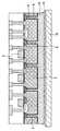
図1に示すように、半導体装置1は、シリコン基板からなる素子形成用のウェハ基板2に、絶縁分離された複数の素子形成領域5を備えている。この素子成形領域5の各々には、半導体基板(ウェハ基板)としてのシリコン基板を用いた能動素子(トランジスタ、ダイオードなど)及び受動素子(抵抗、コンデンサなど)の少なくとも一つが形成されている。例えば、トランジスタの場合には、シリコン基板の導電型と逆の導電型を有する不純物を、シリコン基板の表面側から適宜導入することにより形成された不純物領域7を有する。この不純物領域7が、ソース領域及びドレイン領域となり、ゲート電極9に電圧を印加することにより、その間の領域にチャネルが形成されると、ソース領域とドレイン領域間に電流が流れる。 As shown in FIG. 1, a semiconductor device 1 includes a plurality of
複数の素子形成領域5の周囲を取り囲むようにトレンチ3が形成されている。そのトレンチ3の内部及びウェハ基板2の裏面には、酸化シリコンなどの絶縁材料が堆積されることにより、絶縁層4が形成されている。この絶縁層4によって、複数の素子形成領域5は相互に絶縁分離されている。 A
絶縁層4が埋め込まれるトレンチ3は、後述するようにウェハ基板2の裏面側からエッチングを行うことによって形成される。そのエッチング工程において、ウェハ基板2の表面に形成された絶縁膜であるLOCOS膜6が、エッチングストッパとして利用される。このため、トレンチ3の底部(シリコン基板表面側の先端部)は、LOCOS膜6に接した状態で終端している。エッチングストッパとして、LOCOS膜ではなく、STI膜を利用しても良い。BPSG膜などの層間絶縁膜をエッチングストッパとして用いることも可能ではあるが、シリコン基板とのエッチング選択比を稼ぐためには、上述したLOCOS膜やSTI膜などのサブミクロン以上の厚さを持つ酸化絶縁膜を用いることが好ましい。 The
ウェハ基板2の表面には、上述した能動素子や受動素子の形成後に、熱酸化膜8が形成される。この熱酸化膜8上には、上述したゲート電極9が形成されている。このゲート電極9は、ポリシリコンやタングステン、アルミニウムなどの導電体からなる。その後、BPSG膜やNSG膜からなる層間絶縁膜10を、熱酸化膜8及びゲート電極9上に堆積形成する。さらに、素子形成領域5に形成した能動素子や受動素子の電極11及びパッド12が、層間絶縁膜10及び熱酸化膜8をエッチング除去した部分に形成されている。 A thermal oxide film 8 is formed on the surface of the
次に、図2(a)〜(e)を参照して、上記構成を有する半導体装置1の製造方法について説明する。 Next, with reference to FIGS. 2A to 2E, a method for manufacturing the semiconductor device 1 having the above configuration will be described.
まず、図2(a)に示すように、シリコン基板からなる素子形成用のウェハ基板2を用意する。そして、ウェハ基板2の表面側から、各々の素子形成領域5に所望の素子を形成する。その後、熱酸化膜8、ゲート電極9、層間絶縁膜10、電極11、及びパッシベーション膜13等を形成する。本実施形態による製造方法では、最初に、このような構成を有する半導体素子が、ウェハ基板2の複数個所に形成される。 First, as shown in FIG. 2A, an element forming
次に、図2(b)に示すように、ウェハ基板2の裏面側から、機械的研磨(Mechanical Polish)を行って、ウェハ基板2の厚さを薄くする(薄膜化工程)。この場合、従来のように、半導体基板と絶縁層とが混在した面を研磨するのではなく、半導体基板のみからなる面を研磨すれば良いので、単なる機械的研磨であっても、ウェハ基板2の裏面にクラックや段差を発生させずに、その裏面を均等に研磨することができる。ただし、研磨方法としては、機械的研磨に限らず、化学機械的研磨(Chemical Mechanical Polish)あるいはウェットエッチ、ドライエッチ等の技術を用いても良い。 Next, as shown in FIG. 2B, mechanical polishing is performed from the back side of the
また、薄膜化工程では、例えば、ウェハ基板2の厚さが150μm以下となるまでウェハ基板2を研磨する。このような厚さまでウェハ基板2を薄膜化することにより、トレンチ3の形成や、そのトレンチ3内部への絶縁材料の堆積形成を容易に行うことが可能になる。ただし、ウェハ基板2の厚さが薄くなるに伴って、ウェハ基板2の機械的強度が低下する。従って、ウェハ基板2に割れが発生したり、ウェハ基板2のハンドリングが困難になったりするおそれが生じる。 Further, in the thinning process, for example, the
このため、ウェハ基板2の裏面を研磨することによって薄膜化する際に、通常はウェハ基板2の表面に支持基体を貼り付けて機械強度を保持しておいて薄膜化することが一般的である。しかし、支持基体を貼り付けなくとも良い。この場合、ウェハ基板2の全面を研磨するのではなく、外周部2bによって取り囲まれる中央領域2aだけを研磨することが好ましい。これにより、中央領域2aの厚さだけが薄くなり、外周部2bは、その厚さが薄くされることなく残される。その結果、ウェハ基板2を薄膜化しても、機械的強度の低下を極力抑えることができる。 For this reason, when the
また、支持基体を貼り付けたプロセスでは、貼り合わせに用いられる接着剤の保持温度の制約により、200℃以上の温度をウェハに施すことが困難となる。しかし、上述したように、ウェハ基板2の外周部2bを厚いまま残すことで、支持基体を省略することが可能となるので、200℃より高温の処理を施すことも可能となる。なお、機械的強度の低下を抑制するためには、外周部2bの厚さは250μm以上であることが望ましい。 Further, in the process of attaching the support substrate, it is difficult to apply a temperature of 200 ° C. or higher to the wafer due to the restriction of the holding temperature of the adhesive used for bonding. However, as described above, by leaving the outer peripheral portion 2b of the
次に、図2(c)に示すように、薄膜化されたウェハ基板2に対して、その裏面側からドライエッチング処理を施して、トレンチ3を形成する。このトレンチ3は、各々の素子形成領域5を取り囲むように形成される。このエッチングは、トレンチ3がウェハ基板2の表面側の絶縁膜(LOCOS膜6)まで到達すると、その絶縁膜によってほぼ停止される。 Next, as shown in FIG. 2C, the thinned
ここで、本実施形態では、トレンチ3の形成時点においては、既に、熱酸化膜8や層間絶縁膜10がウェハ基板2の表面上に形成されている。このため、複数の素子形成領域5をそれぞれ取り囲むように、ウェハ基板2を貫通するトレンチ3を形成しても、複数の素子形成領域5を含むウェハ基板2の各領域は、ウェハ基板2の表面上に形成された熱酸化膜8等を介して連結された状態を維持する。従って、従来のように、素子形成領域5の抜け落ちの問題も防止できる。 Here, in the present embodiment, the thermal oxide film 8 and the
次に、図2(d)に示すように、ウェハ基板2の裏面側から、酸化シリコンなどの絶縁材料を直接酸化あるいは化学気相合成法(CVD)等によって堆積形成する。この結果、トレンチ3の内部が絶縁材料によって埋め込まれることにより、トレンチ3の内部に絶縁層4が形成される。このため、ウェハ基板2の複数の素子形成領域5の間に絶縁層4が配置され、隣接する素子形成領域5同士が素子分離される。さらに、トレンチ3の内部から連続する絶縁材料が、ウェハ基板2の裏面にも堆積され、絶縁層4が形成される。これにより、ウェハ基板2の裏面を保護するとともに、絶縁性も確保することができる。 Next, as shown in FIG. 2D, an insulating material such as silicon oxide is deposited from the back side of the
なお、本実施形態では、上述したように、ウェハ基板2の各領域が、ウェハ基板2の表面に形成された熱酸化膜8等によって連結された状態を維持できるので、トレンチ3に充填される絶縁層4によってウェハ基板2の各領域の連結を維持することは必ずしも必要ではない。そのため、トレンチ3内に密に絶縁材料を充填する必要はなく、例えば、トレンチ3の内表面に絶縁材料を堆積させた結果、トレンチ3の内部の中心軸付近に空隙が残っても良い。 In the present embodiment, as described above, each region of the
最後に、図2(e)に示すように、ダイシングによりウェハ基板2を複数のチップ20に分離する分離工程を行う。この分離工程において、厚いまま残された外周部2bはチップ20から切り離される。以上のような工程を経て、本実施形態による、素子分離構造を有する半導体チップ20が完成する。 Finally, as shown in FIG. 2E, a separation process is performed for separating the
(第2実施形態)
次に、本発明の第2実施形態について説明する。図3は、第2実施形態における素子分離構造を有する半導体装置の要部の構成を示す断面図である。(Second Embodiment)
Next, a second embodiment of the present invention will be described. FIG. 3 is a cross-sectional view illustrating a configuration of a main part of a semiconductor device having an element isolation structure according to the second embodiment.
第1実施形態と第2実施形態との相違点は、第2実施形態による半導体装置が、トレンチ3の側壁表面に絶縁材料を堆積させつつ、その中心軸付近の空洞に、比較的低融点の、例えば1100℃以下の融点を有する金属(銅又はアルミニウムなど)からなる導電材料14を充填し、一部のトレンチ3内の導電材料14をウェハ基板2の表面に設けられた電極9aと導通させたことである。ただし、導電材料14として、比較的高融点のポリシリコンなどを用いても良い。その他は、第2実施形態による半導体装置の構造及びその製造方向に関して、第1実施形態と異なるところはない。 The difference between the first embodiment and the second embodiment is that the semiconductor device according to the second embodiment deposits an insulating material on the sidewall surface of the
ここで、素子形成領域5の間に絶縁層4を形成すれば、各々の素子形成領域5に生ずる電気信号のDC成分を遮断することはできる。しかしながら、電気信号のAC成分を完全に遮断することはできないため、そのAC成分の伝播によって誤動作を引き起こす可能性が残る。しかしながら、上述した構成を利用して、素子形成領域5を囲むトレンチ3内の導電材料14の電位を固定することで、隣接する素子形成領域5の間におけるAC成分による電位干渉も抑制することが可能になる。 Here, if the insulating
なお、従来でも、例えば特開平4−154147号公報に示されるように、分離された素子形成領域間で電気的なシールドを得るための構造が提案されている。具体的には、複数の素子形成領域をSOI基板上に形成するとともに、酸化膜で覆われた素子形成領域の間に形成したトレンチにポリシリコン層を埋め込んでいる。 Conventionally, as shown in, for example, Japanese Patent Laid-Open No. 4-154147, a structure for obtaining an electrical shield between separated element forming regions has been proposed. Specifically, a plurality of element formation regions are formed on an SOI substrate, and a polysilicon layer is embedded in a trench formed between element formation regions covered with an oxide film.
しかしながら、このような素子分離構造では、半導体素子を形成する素子形成工程において、既に、素子形成領域の下方及び側方に導体層が形成された状態となる。このため、素子形成工程における高温の熱処理に耐えるため、導体層として、ポリシリコンあるいはタングステンのような高融点金属を用いる必要が生じ、導体層の比抵抗が高くなる。さらに、従来の素子分離構造では、素子形成領域の下方に導体層を配置するためにSOI基板を用いており、高融点の導体層を用いることと相俟って、製造コストが高くなってしまう。 However, in such an element isolation structure, a conductor layer is already formed below and on the side of the element formation region in the element formation process for forming a semiconductor element. For this reason, in order to withstand high-temperature heat treatment in the element formation process, it is necessary to use a refractory metal such as polysilicon or tungsten as the conductor layer, and the specific resistance of the conductor layer is increased. Further, in the conventional element isolation structure, the SOI substrate is used to dispose the conductor layer below the element formation region, and this increases the manufacturing cost in combination with the use of the high melting point conductor layer. .
それに対して、本実施形態では、素子形成領域5への素子形成後にトレンチ3内に導電材料14を充填することができる。従って、導電材料14として、アルミニウムや銅などの比較的低融点の金属を用いることができる。また、単に導電材料14を堆積するだけで素子形成領域5を導電材料14によって取り囲むことができるので、製造コストを低減することができる。 On the other hand, in this embodiment, the
トレンチ3内に導電材料14を充填するには、まず、トレンチ3の中心軸付近に空洞を残しつつ、トレンチ3の側壁表面に絶縁材料を堆積させることによってトレンチ3内表面に絶縁層4を形成する。このとき、ウェハ基板2の裏面にも絶縁材料が堆積されて絶縁層4が形成される。 In order to fill the
次に、ウェハ基板2の表面側に形成された電極9aと熱酸化膜8を介して対向しているトレンチ3において、ウェハ基板2の表面側のトレンチ3の底部に絶縁材料が堆積されていれば、その絶縁材料とともに熱酸化膜8をイオンビームエッチングなどの異方性エッチングにより除去して、トレンチ3の底部において電極9aを露出させる。そして、電極9aが露出されたトレンチ3を含むトレンチ3の中心軸付近の空洞に導電材料14を充填するとともに、ウェハ基板2の裏面上にも導電材料14を堆積させる。これにより、ウェハ基板2の表面側の電極9aと裏面側の導電材料14とがトレンチ3内部の導電材料14を介して電気的に導通可能となり、その結果、ウェハ基板2の裏面側の導電材料14に接続され、トレンチ3内部で終端している導電材料14も、ウェハ基板2の表面側の電極9aと電気的に接続された構成を得ることができる。 Next, in the
このような構成において、ウェハ基板2の表面側の電極9aに所定電位を印加することにより、この電極9aに電気的に接続された、トレンチ3内部及びウェハ基板2の裏面側の導電材料14は全てその所定電位に固定される。従って、隣接する素子形成領域5の間におけるAC成分による電位干渉も抑制することができる。なお、所定電位は、接地電位に固定することが好ましい。これにより、電力消費を抑制しつつ、隣接する素子形成領域における電位干渉を防止することができる。 In such a configuration, by applying a predetermined potential to the
(第3実施形態)
次に、本発明の第3実施形態について説明する。図4は、第3実施形態における素子分離構造を有する半導体装置の要部の構成を示す断面図である。(Third embodiment)
Next, a third embodiment of the present invention will be described. FIG. 4 is a cross-sectional view showing a configuration of a main part of a semiconductor device having an element isolation structure in the third embodiment.
本実施形態においては、素子形成領域5の1つが、縦型素子形成領域16となっており、ウェハ基板2の表面側に表面電極9bが形成され、裏面側に裏面電極15が形成されている。さらに、裏面電極15は、導電性の接合部材18を介して、導体プレート19に接合されている。その他の構成は、図示していないが、ウェハ基板2の表面側に形成された電極9aによってトレンチ3内部及びウェハ基板2の裏面上に堆積された導電材料14を所定電位に固定する構成も含め、第2実施形態による半導体装置と同様である。 In the present embodiment, one of the
ウェハ基板2の裏面側に堆積形成された裏面電極15は、例えば導電材料14と同じ材料によって形成され、裏面電極15と導電材料14との間には、絶縁を確保するために絶縁層17が形成されている。このような裏面電極構造を得るためには、まず、ウェハ基板2の裏面全体に導電材料14を所定の厚さだけ堆積形成する。その後、縦型素子形成領域の裏面電極15の形成位置及びその周囲の領域の導電材料14をエッチングにより除去する。次に、酸化シリコンなどの絶縁材料を化学気相合成法(CVD)等によって堆積することによって絶縁層17を形成する。そして、裏面電極15の形成位置の絶縁層17をエッチング除去した後に、再び、ウェハ基板2の裏面に導電材料を堆積させ、裏面電極15を形成する。なお裏面電極15の形成位置の絶縁層17を除去する際、以前に形成された絶縁層4も同時に除去される。 The
その後、例えばはんだ、銀ペースト、もしくは金属ナノ粒子からなる接合部材18により、裏面電極15を導体プレート19に接合する。なお、導体プレート19は、半導体チップ20がパッケージ化される際に、半導体チップ20を支持する金属フレームであったり、半導体チップ20がマザー基板に実装される際の、マザー基板表面に設けられた銅箔などである。 Thereafter, the
つまり、第3実施形態の半導体装置では、ウェハ基板2の裏面上において、導電材料が絶縁層17を介して2層に積層されるとともに、素子形成領域5を電気的にシールドする導電材料14は、絶縁層17により、ウェハ基板2に接する面と反対側の面に形成された導電材料の層と絶縁される一方、縦型素子形成領域16の裏面電極15となる導電材料は、絶縁層17を貫通してウェハ基板2に接する面と反対側の面に形成された導電材料の層に電気的に接続されている。従って、ウェハ基板2に接する面と反対側の面に形成された導電材料は、裏面電極15の一部となる。 That is, in the semiconductor device of the third embodiment, the
以上のように構成された第3実施形態の半導体装置によれば、ウェハ基板2の裏面側に、縦型素子形成領域16の裏面電極15を形成する場合であっても、それ以外の素子形成領域5については、各素子形成領域5を電気的にシールドするための導電材料14をウェハ基板2の裏面に形成することが可能になる。そして、裏面電極15に導体プレート19を接合することにより、導体プレート19を裏面電極15の接続端子として利用することができる。さらに、導体プレート19により、素子形成領域5,16の放熱が促進されるので、放熱性を向上することができる。 According to the semiconductor device of the third embodiment configured as described above, even when the
次に、第3実施形態の変形例について説明する。図5は、第3実施形態の変形例による半導体装置の要部の構成を示す断面図である。上述した第3実施形態では、導電材料が、絶縁層17を挟んで2層に形成されていたが、図5に示された変形例では、素子形成領域5を電気的にシールドする導電材料14は一層構造であり、縦型素子形成領域16の裏面電極15aは、導電材料14よりも厚く形成されている。裏面電極15aと導電材料14との厚さの差の分だけ、導電材料14上に絶縁層17aが形成されている。従って、裏面電極15aと絶縁層17aとは、ウェハ基板2に接する面と反対側の面において、同一面を形成している。この裏面電極15aと絶縁層17aとからなる面が、接合部材18を介して導体プレート19に接合されている。 Next, a modification of the third embodiment will be described. FIG. 5 is a cross-sectional view showing a configuration of a main part of a semiconductor device according to a modification of the third embodiment. In the third embodiment described above, the conductive material is formed in two layers with the insulating
このような構成しても、裏面電極15aは、絶縁層17aによって導電材料14と絶縁され、かつ縦型素子形成領域16の裏面電極15aは、素子形成領域5を電気的にシールドする導電材料14よりも厚さが厚いため、導体プレート19が、縦型素子形成領域16の裏面電極15aのみに電気的に接続される。従って、導体プレート19を裏面電極15aの接続端子として利用することができる。 Even in such a configuration, the
(第4実施形態)
次に、本発明の第4実施形態について説明する。上述した第2及び第3実施形態では、ウェハ基板2の表面側に設けた電極9aとトレンチ3内の導電材料14とを導通させることにより、トレンチ3内の導電材料14及びウェハ基板2の裏面側の導電材料14の電位を所定電位に固定した。しかしながら、ウェハ基板2の表面側には、各素子の電極配線等を形成する必要があるため、電極9aの配置箇所は制限される。すると、トレンチ3内における導電材料14の径は細く、インピーダンスが相対的に高くなるので、特に、電極9aに直接接続されていないトレンチ3内の導電材料14の電位が、安定して所定電位に固定できない場合がある。(Fourth embodiment)
Next, a fourth embodiment of the present invention will be described. In the second and third embodiments described above, the
その点に鑑みて、本実施形態による半導体装置では、ウェハ基板2の裏面側に接合した導体プレート19を利用して、トレンチ3内部及びウェハ基板2の裏面の導電材料14を所定電位に固定するものである。 In view of this point, in the semiconductor device according to the present embodiment, the
図6は、第4実施形態における素子分離構造を有する半導体装置の要部の構成を示す断面図である。図6に示すように、導電材料14が、トレンチ3内部及びウェハ基板2の裏面に堆積形成されている。本実施形態では、このように堆積形成されたウェハ基板2の裏面の導電材料14に、接合部材18を介して導体プレート19を接合する。この導体プレート19には、例えば所定電位として接地電位が与えられる。これにより、導体プレート19を介して、トレンチ3内部及びウェハ基板2の裏面の導電材料14の電位が所定電位に固定される。 FIG. 6 is a cross-sectional view showing a configuration of a main part of a semiconductor device having an element isolation structure in the fourth embodiment. As shown in FIG. 6, a
特に、本実施形態では、ウェハ基板2の裏面において、少なくともトレンチ3の形成位置を網羅するように接合される導体プレート19により、導電材料14の電位を固定している。換言すれば、トレンチ3内の細径の導電材料14を経由して、他のトレンチ3内の導電材料14の電位を固定する必要がないので、低インピーダンスでの電気的接続が可能になる。このため、トレンチ3内部及びウェハ基板2の裏面の導電材料14の電位を安定して所定電位に保つことができる。 In particular, in the present embodiment, the potential of the
次に、第4実施形態の変形例について説明する。図7は、第4実施形態の変形例による半導体装置の要部の構成を示す断面図である。図7に示す変形例では、素子形成領域5の一部の領域が縦型素子形成領域16となっている。このような縦型素子形成領域16の裏面電極15をウェハ基板2の裏面に設けつつ、同時にウェハ基板2の裏面側の導体プレート19を用いて、トレンチ3内部及びウェハ基板2の裏面の導電材料14に所定電位を与えるべく、導体プレート19が、裏面電極15に接続される電極プレート19aと導電材料14に接続される導電プレート19bとに分割されている。そして、電極プレート19aと導電プレート19bとの間には絶縁部19cが設けられており、電極プレート19aと導電プレート19bとは絶縁分離されている。 Next, a modification of the fourth embodiment will be described. FIG. 7 is a cross-sectional view showing a configuration of a main part of a semiconductor device according to a modification of the fourth embodiment. In the modification shown in FIG. 7, a part of the
このような構成を採用することで、導体プレート19を用いて、トレンチ3内部及びウェハ基板2裏面の導電材料14の電位を固定しつつ、縦型素子形成領域16の裏面電極15の接続端子としての役割も発揮させることができる。 By adopting such a configuration, the
なお、導体プレート19は、電極プレート19aと導電プレート19bとが絶縁部19cを介して連結された構成のものを予め用意して、ウェハ基板2に接合しても良いし、導体プレート19をウェハ基板2に接合した後に、絶縁部19cに対応する領域を除去し、その除去部分に絶縁材を挿入して形成しても良い。 The
以上、本発明による好ましい実施形態について説明したが、本発明は、上述した実施形態になんら制限されることなく、本発明の主旨を逸脱しない範囲において、種々変形して実施することが可能である。 The preferred embodiments according to the present invention have been described above. However, the present invention is not limited to the above-described embodiments, and various modifications can be made without departing from the spirit of the present invention. .
例えば、図8に示すように、トレンチ3内部に導電材料14を堆積させた結果、トレンチ3内部の中心軸付近に空隙が残っても良い。トレンチ3内部を導電材料14で完全に埋めようとすると、導電材料14の堆積工程に長時間を要しコストが高くなってしまう。また、トレンチ14内部の導電材料14は、上述したように隣接する素子形成領域5間の電位干渉を防止するためのものであるため、多少空隙が残っても、その機能に支障はない。 For example, as shown in FIG. 8, as a result of depositing the
また、図9に示すように、トレンチ3をウェハ基板2に形成する際、トレンチ3は、素子形成領域5における不純物の拡散層7aと交差しても良い。これにより、素子面積を小さくすることができるので、半導体チップ20のコストを低減することができる。 As shown in FIG. 9, when the
さらに、例えば、素子形成領域5を取り囲むようにトレンチ3を形成し、そのトレンチ3の内部に絶縁層4を形成して素子分離する場合であっても、種々の素子形成領域の配置例が考えられる。 Further, for example, even when the
例えば、図10において、素子形成領域21は、その回りを絶縁層が形成された1本のトレンチ22で取り囲まれているが、他の素子形成領域と隣接しておらず、その間に分離領域(フィールド領域)23が設けられている。この場合、フィールド領域23と素子形成領域21との間に電圧を印加して、トレンチ22の絶縁性を確認する試験を行うことが可能である。さらに、フィールド領域23の電位を固定することにより、素子形成領域21の電位干渉を抑制することも可能となる。 For example, in FIG. 10, the
また、素子形成領域24のように、一本のトレンチ25で仕切られつつ、複数の素子形成領域24を隣接して配置しても良い、この場合、高い密度で素子形成領域24を配置することが可能となり、一枚のウェハ基板2からより多くの半導体チップを得ることができる。 Further, like the
さらに、素子形成領域26のように、複数本のトレンチ27,28で素子形成領域26を取り囲むことにより、素子分離を行っても良い。この場合、複数本のトレンチ27,28に電圧を分担させることができるので、素子形成領域26には、高い電圧が印加される素子を配置することができる。 Further, element isolation may be performed by surrounding the
1 半導体装置
2 ウェハ基板
3 トレンチ
4 絶縁層
5 素子形成領域
6 LOCOS膜
7 不純物領域
8 熱酸化膜
9 ゲート電極
10 層間絶縁膜
11 電極DESCRIPTION OF SYMBOLS 1
Claims (19)
Translated fromJapanese表面及び裏面を有するシリコン基板からなる半導体基板を準備する工程と、
前記半導体基板の表面側において、前記半導体基板の複数の素子形成領域のそれぞれに少なくとも1つの能動素子または受動素子を形成するとともに、前記半導体基板の表面に絶縁膜を形成する工程と、
前記半導体基板の裏面側から、当該半導体基板の厚みを薄くする工程と、
前記半導体基板の厚みを薄くした後に、前記複数の素子形成領域をそれぞれ取り囲むように、前記半導体基板の裏面側から、前記半導体基板の表面に形成された絶縁膜に達するトレンチを形成する工程と、
前記トレンチの内表面に、直接酸化あるいはCVDにより酸化シリコンからなる絶縁材料を堆積させることによって前記トレンチ内に絶縁層を形成して、前記素子形成領域を絶縁分離する工程と、を備え、
前記トレンチの内表面に堆積される絶縁材料が、前記半導体基板の裏面上にも堆積され、裏面上に残されることを特徴とする半導体装置の製造方法。A method of manufacturing a semiconductor device, wherein at least one of an active element and a passive element using a semiconductor substrate is formed in each of a plurality of element formation regions isolated and separated in one semiconductor substrate,
Preparing a semiconductor substratecomprising asilicon substrate having afront surface and a back surface;
Forming at least one active element or passive element in each of a plurality of element formation regions of the semiconductor substrate on the surface side of the semiconductor substrate, and forming an insulating film on the surface of the semiconductor substrate;
Reducing the thickness of the semiconductor substrate from the back side of the semiconductor substrate;
Forming a trench reaching the insulating film formed on the surface of the semiconductor substrate from the back side of the semiconductor substrate so as to surround each of the plurality of element formation regions after reducing the thickness of the semiconductor substrate;
Forming an insulating layer in the trench by depositing an insulating material made ofsilicon oxide by direct oxidation or CVD on the inner surface ofthe trench, and isolating and isolating the element formation region,
An insulating material deposited on the inner surface of the trench is deposited on the back surface of the semiconductor substrate and is left on the back surface .
表面及び裏面を有する半導体基板を準備する工程と、
前記半導体基板の表面側において、前記半導体基板の複数の素子形成領域のそれぞれに少なくとも1つの能動素子または受動素子を形成し、前記半導体基板の表面に絶縁膜を形成し、さらに、その絶縁膜上に導電体を形成する工程と、
前記半導体基板の裏面側から、当該半導体基板の厚みを薄くする工程と、
前記半導体基板の厚みを薄くした後に、前記半導体基板の裏面側から前記半導体基板の表面に形成された絶縁膜に達するトレンチを形成する工程と、
少なくとも前記トレンチの中心軸付近に空洞を残しつつ、当該トレンチの側壁表面に絶縁材料を堆積させることによって前記トレンチ内に絶縁層を形成して前記素子形成領域を絶縁分離するとともに、半導体基板の裏面にも前記絶縁材料を堆積させる工程と、
前記半導体基板の表面側に形成された前記導電体と前記絶縁膜を介して対向しているトレンチにおいて、前記半導体基板の表面側のトレンチ底部の前記絶縁膜を除去して、前記導電体を露出させる工程と、
前記導電体が露出されたトレンチを含む、前記トレンチの中心軸付近の空洞に導電材料を堆積させるとともに、前記半導体基板の裏面上にも前記導電材料を堆積させる工程と、を備え、
前記半導体基板の表面側の導電体と裏面側の導電材料とを前記トレンチ内部の導電材料を介して電気的に導通可能とすることを特徴とする半導体装置の製造方法。A method of manufacturing a semiconductor device, wherein at least one of an active element and a passive element using a semiconductor substrate is formed in each of a plurality of element formation regions isolated and separated in one semiconductor substrate,
Preparing a semiconductor substrate having a front surface and a back surface;
On the surface side of the semiconductor substrate, at least one active element or passive element is formed in each of a plurality of element formation regions of the semiconductor substrate, an insulating film is formed on the surface of the semiconductor substrate, and further on the insulating film Forming a conductor on the substrate,
Reducing the thickness of the semiconductor substrate from the back side of the semiconductor substrate;
Forming a trench reaching the insulating film formed on the surface of the semiconductor substrate from the back side of the semiconductor substrate after reducing the thickness of the semiconductor substrate;
While leaving a cavity at least near the central axis of the trench, an insulating material is deposited on the sidewall surface of the trench to form an insulating layer in the trench to insulate and isolate the element formation region, and to backside the semiconductor substrate Depositing the insulating material on the substrate;
In the trench facing the conductor formed on the surface side of the semiconductor substrate through the insulating film, the insulating film at the bottom of the trench on the surface side of the semiconductor substrate is removed to expose the conductor A process of
Depositing a conductive material in a cavity near the central axis of the trench, including a trench in which the conductor is exposed, and depositing the conductive material also on a back surface of the semiconductor substrate,
A method of manufacturing a semiconductor device, wherein a conductor on a front surface side and a conductive material on a back surface side of the semiconductor substrate can be electrically conducted through a conductive material in the trench.
表面及び裏面を有する半導体基板を準備する工程と、
前記半導体基板の表面側において、前記半導体基板の複数の素子形成領域のそれぞれに少なくとも1つの能動素子または受動素子を形成し、前記半導体基板の表面に絶縁膜を形成する工程と、
前記半導体基板の裏面側から、当該半導体基板の厚みを薄くする工程と、
前記半導体基板の厚みを薄くした後に、前記半導体基板の裏面側から前記半導体基板の表面に形成された絶縁膜に達するトレンチを形成する工程と、
少なくとも前記トレンチの中心軸付近に空洞を残しつつ、当該トレンチの側壁表面に絶縁材料を堆積させることによって前記トレンチ内に絶縁層を形成して前記素子形成領域を絶縁分離するとともに、半導体基板の裏面にも前記絶縁材料を堆積させる工程と、
前記トレンチの中心軸付近の空洞に導電材料を堆積させるとともに、前記半導体基板の裏面上にも前記導電材料を堆積させる工程と、を備え、
前記トレンチ内部の導電材料と前記半導体基板裏面上の導電材料との電位を固定することによって、前記素子形成領域を電気的にシールド可能としたことを特徴とする半導体装置の製造方法。A method of manufacturing a semiconductor device, wherein at least one of an active element and a passive element using a semiconductor substrate is formed in each of a plurality of element formation regions isolated and separated in one semiconductor substrate,
Preparing a semiconductor substrate having a front surface and a back surface;
Forming at least one active element or passive element in each of a plurality of element formation regions of the semiconductor substrate on the surface side of the semiconductor substrate, and forming an insulating film on the surface of the semiconductor substrate;
Reducing the thickness of the semiconductor substrate from the back side of the semiconductor substrate;
Forming a trench reaching the insulating film formed on the surface of the semiconductor substrate from the back side of the semiconductor substrate after reducing the thickness of the semiconductor substrate;
While leaving a cavity at least near the central axis of the trench, an insulating material is deposited on the sidewall surface of the trench to form an insulating layer in the trench to insulate and isolate the element formation region, and to backside the semiconductor substrate Depositing the insulating material on the substrate;
Depositing a conductive material in a cavity near the central axis of the trench, and depositing the conductive material also on the back surface of the semiconductor substrate,
A method of manufacturing a semiconductor device, wherein the element forming region can be electrically shielded by fixing a potential between a conductive material in the trench and a conductive material on the back surface of the semiconductor substrate.
前記半導体基板の表面側に形成された前記導電体と前記絶縁膜を介して対向しているトレンチにおいて、前記半導体基板の表面側のトレンチ底部の前記絶縁膜を除去して、前記導電体を露出させる工程と、をさらに備え、
前記導電材料を堆積させる工程において、前記トレンチ内に堆積される前記導電材料と前記半導体基板の表面側に形成された前記導電体とを電気的に接続し、前記導電体を介して、前記トレンチ内部の導電材料と前記半導体基板裏面上の導電材料との電位を固定することを特徴とする請求項10に記載の半導体装置の製造方法。Forming a conductor on the insulating film on the surface of the semiconductor substrate;
In the trench facing the conductor formed on the surface side of the semiconductor substrate through the insulating film, the insulating film at the bottom of the trench on the surface side of the semiconductor substrate is removed to expose the conductor And a step of causing
In the step of depositing the conductive material, the conductive material deposited in the trench is electrically connected to the conductor formed on the surface side of the semiconductor substrate, and the trench is interposed via the conductor. 11. The method of manufacturing a semiconductor device according to claim10 , wherein a potential between an internal conductive material and a conductive material on the back surface of the semiconductor substrate is fixed.
前記導電材料を堆積させる工程において、前記素子形成領域を電気的にシールドするための導電材料と、前記縦型素子形成領域の裏面電極となる導電材料とが前記半導体基板の裏面上に堆積されるとともに、前記素子形成領域を電気的にシールドするための導電材料と、前記縦型素子形成領域の裏面電極となる導電材料との間に絶縁層が形成されることを特徴とする請求項11に記載の半導体装置の製造方法。The element formation region includes a vertical element formation region in which an electrode is formed on the back side of the semiconductor substrate,
In the step of depositing the conductive material, a conductive material for electrically shielding the element formation region and a conductive material to be a back electrode of the vertical element formation region are deposited on the back surface of the semiconductor substrate. with a conductive material for electrically shielding the element formation regions, to claim11, wherein an insulating layer is formed between the conductive material serving as a back surface electrode of the vertical element formation region The manufacturing method of the semiconductor device of description.
前記縦型素子形成領域の裏面電極となる導電材料は、前記素子形成領域を電気的にシールドするための導電材料よりも厚く形成されることにより、前記導体プレートが、前記縦型素子形成領域の裏面電極となる導電材料のみに電気的に接続されることを特徴とする請求項12に記載の半導体装置の製造方法。Further comprising the step of bonding the conductive material deposited on the back surface of the semiconductor substrate onto the conductor plate;
The conductive material to be the back electrode of the vertical element formation region is formed thicker than the conductive material for electrically shielding the element formation region, so that the conductor plate is formed in the vertical element formation region. The method of manufacturing a semiconductor device according to claim12 , wherein the semiconductor device is electrically connected only to a conductive material to be a back electrode.
前記半導体基板の裏面上において、前記導電材料は絶縁層を介して2層に積層されるとともに、前記素子形成領域を電気的にシールドする導電材料は、前記絶縁層により、前記半導体基板に接する面と反対側の面に形成された導電材料の層と絶縁される一方、前記縦型素子形成領域の裏面電極となる導電材料は、前記絶縁層を貫通して前記半導体基板に接する面と反対側の面に形成された導電材料の層に電気的に接続されることにより、前記導体プレートが、前記縦型素子形成領域の裏面電極となる導電材料のみに電気的に接続されることを特徴とする請求項12に記載の半導体装置の製造方法。Further comprising the step of bonding the conductive material deposited on the back surface of the semiconductor substrate onto the conductor plate;
On the back surface of the semiconductor substrate, the conductive material is laminated in two layers via an insulating layer, and the conductive material that electrically shields the element formation region is a surface in contact with the semiconductor substrate by the insulating layer. While being insulated from the conductive material layer formed on the surface opposite to the surface, the conductive material to be the back surface electrode of the vertical element forming region is opposite to the surface contacting the semiconductor substrate through the insulating layer The conductive plate is electrically connected to only the conductive material that becomes the back electrode of the vertical element formation region by being electrically connected to the layer of the conductive material formed on the surface of the vertical element. A method for manufacturing a semiconductor device according to claim12 .
前記導体プレートは、前記素子形成領域を電気的にシールドするための導電材料が接合される領域と、前記縦型素子形成領域の裏面電極となる導電材料が接合される領域との間に絶縁材料が挿入され、当該絶縁材料により電気的に分割された分割プレートであることを特徴とする請求項15に記載の半導体装置の製造方法。The element formation region includes a vertical element formation region in which an electrode is formed on the back side of the semiconductor substrate,
The conductor plate is an insulating material between a region where a conductive material for electrically shielding the element formation region is bonded and a region where a conductive material to be a back electrode of the vertical element formation region is bonded.16. The method of manufacturing a semiconductor device according to claim15 , wherein a dividing plate is inserted and electrically divided by the insulating material.
Priority Applications (3)
| Application Number | Priority Date | Filing Date | Title |
|---|---|---|---|
| JP2008106014AJP4687742B2 (en) | 2007-08-27 | 2008-04-15 | Manufacturing method of semiconductor device |
| EP08014382.9AEP2031653B1 (en) | 2007-08-27 | 2008-08-12 | Manufacturing method for a semiconductor device having multiple element formation regions |
| US12/230,209US7833876B2 (en) | 2007-08-27 | 2008-08-26 | Semiconductor device having multiple element formation regions and manufacturing method thereof |
Applications Claiming Priority (3)
| Application Number | Priority Date | Filing Date | Title |
|---|---|---|---|
| JP2007220240 | 2007-08-27 | ||
| JP2007220240 | 2007-08-27 | ||
| JP2008106014AJP4687742B2 (en) | 2007-08-27 | 2008-04-15 | Manufacturing method of semiconductor device |
Related Child Applications (1)
| Application Number | Title | Priority Date | Filing Date |
|---|---|---|---|
| JP2010047118ADivisionJP5287768B2 (en) | 2007-08-27 | 2010-03-03 | Semiconductor device |
Publications (2)
| Publication Number | Publication Date |
|---|---|
| JP2009076848A JP2009076848A (en) | 2009-04-09 |
| JP4687742B2true JP4687742B2 (en) | 2011-05-25 |
Family
ID=40611499
Family Applications (2)
| Application Number | Title | Priority Date | Filing Date |
|---|---|---|---|
| JP2008106014AExpired - Fee RelatedJP4687742B2 (en) | 2007-08-27 | 2008-04-15 | Manufacturing method of semiconductor device |
| JP2010047118AExpired - Fee RelatedJP5287768B2 (en) | 2007-08-27 | 2010-03-03 | Semiconductor device |
Family Applications After (1)
| Application Number | Title | Priority Date | Filing Date |
|---|---|---|---|
| JP2010047118AExpired - Fee RelatedJP5287768B2 (en) | 2007-08-27 | 2010-03-03 | Semiconductor device |
Country Status (1)
| Country | Link |
|---|---|
| JP (2) | JP4687742B2 (en) |
Families Citing this family (3)
| Publication number | Priority date | Publication date | Assignee | Title |
|---|---|---|---|---|
| JP2012182336A (en)* | 2011-03-02 | 2012-09-20 | Toshiba Corp | Semiconductor device |
| JP5902010B2 (en)* | 2012-03-19 | 2016-04-13 | トランスフォーム・ジャパン株式会社 | Compound semiconductor device and manufacturing method thereof |
| JP6077252B2 (en)* | 2012-09-28 | 2017-02-08 | エスアイアイ・セミコンダクタ株式会社 | Semiconductor integrated circuit device |
Family Cites Families (14)
| Publication number | Priority date | Publication date | Assignee | Title |
|---|---|---|---|---|
| US4612408A (en)* | 1984-10-22 | 1986-09-16 | Sera Solar Corporation | Electrically isolated semiconductor integrated photodiode circuits and method |
| JPS62130537A (en)* | 1985-12-03 | 1987-06-12 | Toshiba Corp | Isolation method between integrated circuit elements |
| JPH0817177B2 (en)* | 1987-11-16 | 1996-02-21 | 日産自動車株式会社 | Semiconductor device |
| US5354695A (en)* | 1992-04-08 | 1994-10-11 | Leedy Glenn J | Membrane dielectric isolation IC fabrication |
| JPH0770587B2 (en)* | 1991-09-05 | 1995-07-31 | 工業技術院長 | Method for manufacturing semiconductor integrated circuit structure |
| JPH1027767A (en)* | 1996-07-11 | 1998-01-27 | Sanyo Electric Co Ltd | Manufacture of semiconductor device |
| JPH11195712A (en)* | 1997-11-05 | 1999-07-21 | Denso Corp | Semiconductor device and manufacturing method thereof |
| FR2782840B1 (en)* | 1998-08-25 | 2003-09-05 | Commissariat Energie Atomique | ELECTRONIC CIRCUIT AND METHOD FOR MAKING AN INTEGRATED ELECTRONIC CIRCUIT COMPRISING AT LEAST ONE ELECTRONIC POWER COMPONENT IN A SUBSTRATE PLATE |
| JP2001144173A (en)* | 1999-11-17 | 2001-05-25 | Denso Corp | Method of manufacturing semiconductor device |
| JP4271625B2 (en)* | 2004-06-30 | 2009-06-03 | 株式会社フジクラ | Semiconductor package and manufacturing method thereof |
| JP5048230B2 (en)* | 2005-03-30 | 2012-10-17 | オンセミコンダクター・トレーディング・リミテッド | Semiconductor device and manufacturing method thereof |
| JP2007035729A (en)* | 2005-07-22 | 2007-02-08 | Matsushita Electric Ind Co Ltd | Semiconductor integrated circuit device |
| JP2007165693A (en)* | 2005-12-15 | 2007-06-28 | Denso Corp | Semiconductor device |
| JP5217348B2 (en)* | 2006-12-06 | 2013-06-19 | 株式会社デンソー | Semiconductor device |
- 2008
- 2008-04-15JPJP2008106014Apatent/JP4687742B2/ennot_activeExpired - Fee Related
- 2010
- 2010-03-03JPJP2010047118Apatent/JP5287768B2/ennot_activeExpired - Fee Related
Also Published As
| Publication number | Publication date |
|---|---|
| JP5287768B2 (en) | 2013-09-11 |
| JP2010118711A (en) | 2010-05-27 |
| JP2009076848A (en) | 2009-04-09 |
Similar Documents
| Publication | Publication Date | Title |
|---|---|---|
| US7833876B2 (en) | Semiconductor device having multiple element formation regions and manufacturing method thereof | |
| US8466054B2 (en) | Thermal conduction paths for semiconductor structures | |
| JP5048230B2 (en) | Semiconductor device and manufacturing method thereof | |
| US7994048B2 (en) | Method of manufacturing a through electrode | |
| TWI397972B (en) | Semiconductor device manufacturing method | |
| US7498636B2 (en) | Semiconductor device and method of manufacturing the same | |
| US20160181228A1 (en) | Semiconductor device and method for manufacturing same | |
| JP5972537B2 (en) | Semiconductor device and manufacturing method thereof | |
| JP2013115382A (en) | Semiconductor device and manufacturing method thereof | |
| US20160172301A1 (en) | Semiconductor device and manufacturing method therefor | |
| JP4945545B2 (en) | Manufacturing method of semiconductor device | |
| US9698103B2 (en) | Semiconductor device and manufacturing method therefor | |
| US20200098659A1 (en) | High resistivity wafer with heat dissipation structure and method of making the same | |
| JP4687742B2 (en) | Manufacturing method of semiconductor device | |
| JP2005158959A (en) | Semiconductor device | |
| JP5271562B2 (en) | Semiconductor device and manufacturing method of semiconductor device | |
| TWI643304B (en) | Bauelement mit durchkontaktierung und verfahren zur herstellungcomponent with through-contact and process for its production | |
| CN112563241A (en) | Semiconductor device with a plurality of semiconductor chips | |
| US7375397B2 (en) | Semiconductor device having an SOI structure and method for manufacturing the same | |
| TW200937574A (en) | Semiconductor device and method for manufacturing same | |
| TWI251926B (en) | Wiring substrate, manufacturing method thereof, and semiconductor device | |
| JP2010114350A (en) | Method of manufacturing semiconductor device, and semiconductor device | |
| CN108511415B (en) | Method for manufacturing electronic assembly | |
| JP2017120851A (en) | Semiconductor device and manufacturing method of semiconductor device | |
| CN100505300C (en) | Semiconductor device and manufacturing method thereof |
Legal Events
| Date | Code | Title | Description |
|---|---|---|---|
| A621 | Written request for application examination | Free format text:JAPANESE INTERMEDIATE CODE: A621 Effective date:20090115 | |
| A977 | Report on retrieval | Free format text:JAPANESE INTERMEDIATE CODE: A971007 Effective date:20090901 | |
| A131 | Notification of reasons for refusal | Free format text:JAPANESE INTERMEDIATE CODE: A131 Effective date:20100106 | |
| A521 | Request for written amendment filed | Free format text:JAPANESE INTERMEDIATE CODE: A523 Effective date:20100303 | |
| TRDD | Decision of grant or rejection written | ||
| A01 | Written decision to grant a patent or to grant a registration (utility model) | Free format text:JAPANESE INTERMEDIATE CODE: A01 Effective date:20110118 | |
| A01 | Written decision to grant a patent or to grant a registration (utility model) | Free format text:JAPANESE INTERMEDIATE CODE: A01 | |
| A61 | First payment of annual fees (during grant procedure) | Free format text:JAPANESE INTERMEDIATE CODE: A61 Effective date:20110131 | |
| R151 | Written notification of patent or utility model registration | Ref document number:4687742 Country of ref document:JP Free format text:JAPANESE INTERMEDIATE CODE: R151 | |
| FPAY | Renewal fee payment (event date is renewal date of database) | Free format text:PAYMENT UNTIL: 20140225 Year of fee payment:3 | |
| R250 | Receipt of annual fees | Free format text:JAPANESE INTERMEDIATE CODE: R250 | |
| R250 | Receipt of annual fees | Free format text:JAPANESE INTERMEDIATE CODE: R250 | |
| R250 | Receipt of annual fees | Free format text:JAPANESE INTERMEDIATE CODE: R250 | |
| R250 | Receipt of annual fees | Free format text:JAPANESE INTERMEDIATE CODE: R250 | |
| R250 | Receipt of annual fees | Free format text:JAPANESE INTERMEDIATE CODE: R250 | |
| R250 | Receipt of annual fees | Free format text:JAPANESE INTERMEDIATE CODE: R250 | |
| LAPS | Cancellation because of no payment of annual fees |