JP4686435B2 - Arithmetic unit - Google Patents
Arithmetic unitDownload PDFInfo
- Publication number
- JP4686435B2 JP4686435B2JP2006292960AJP2006292960AJP4686435B2JP 4686435 B2JP4686435 B2JP 4686435B2JP 2006292960 AJP2006292960 AJP 2006292960AJP 2006292960 AJP2006292960 AJP 2006292960AJP 4686435 B2JP4686435 B2JP 4686435B2
- Authority
- JP
- Japan
- Prior art keywords
- data
- pattern
- rearrangement
- register
- instruction
- Prior art date
- Legal status (The legal status is an assumption and is not a legal conclusion. Google has not performed a legal analysis and makes no representation as to the accuracy of the status listed.)
- Expired - Fee Related
Links
Images


Classifications
- G—PHYSICS
- G06—COMPUTING OR CALCULATING; COUNTING
- G06F—ELECTRIC DIGITAL DATA PROCESSING
- G06F9/00—Arrangements for program control, e.g. control units
- G06F9/06—Arrangements for program control, e.g. control units using stored programs, i.e. using an internal store of processing equipment to receive or retain programs
- G06F9/30—Arrangements for executing machine instructions, e.g. instruction decode
- G06F9/30003—Arrangements for executing specific machine instructions
- G06F9/30007—Arrangements for executing specific machine instructions to perform operations on data operands
- G06F9/30032—Movement instructions, e.g. MOVE, SHIFT, ROTATE, SHUFFLE
- G—PHYSICS
- G06—COMPUTING OR CALCULATING; COUNTING
- G06F—ELECTRIC DIGITAL DATA PROCESSING
- G06F9/00—Arrangements for program control, e.g. control units
- G06F9/06—Arrangements for program control, e.g. control units using stored programs, i.e. using an internal store of processing equipment to receive or retain programs
- G06F9/30—Arrangements for executing machine instructions, e.g. instruction decode
- G06F9/30003—Arrangements for executing specific machine instructions
- G06F9/30007—Arrangements for executing specific machine instructions to perform operations on data operands
- G06F9/30036—Instructions to perform operations on packed data, e.g. vector, tile or matrix operations
Landscapes
- Engineering & Computer Science (AREA)
- Software Systems (AREA)
- Theoretical Computer Science (AREA)
- Physics & Mathematics (AREA)
- General Engineering & Computer Science (AREA)
- General Physics & Mathematics (AREA)
- Mathematical Physics (AREA)
- Advance Control (AREA)
- Executing Machine-Instructions (AREA)
Description
Translated fromJapanese本発明は、演算装置に係り、特に、SIMD(Single-Instruction/Multiple-Data)演算を行うことが可能な演算装置に関する。 The present invention relates to an arithmetic device, and more particularly to an arithmetic device capable of performing SIMD (Single-Instruction / Multiple-Data) arithmetic.
1つの命令で複数のデータを並列に演算することが可能なSIMD演算を行う場合、メモリから読み出したデータを並列に演算可能となるよう、データの並べ替えという手順を必要とする。このデータの並べ替えに複数サイクルを費やしてしまうと、SIMD演算器が演算を行っていない時間が増加し、SIMD演算器が本来持っている性能を十分発揮することができない。 When performing a SIMD operation that can calculate a plurality of data in parallel with one instruction, a procedure of data rearrangement is required so that the data read from the memory can be calculated in parallel. If a plurality of cycles are spent for rearranging the data, the time during which the SIMD computing unit is not performing computation increases, and the performance inherent in the SIMD computing unit cannot be fully exhibited.
SIMD演算を行うことが可能なプロセッサは、演算命令だけでなく、データを並べ替える命令も同時に実装されていることが多い。しかし、予め用意されている命令は、命令数の制限から単純なパターンに限定されてしまう。このため、そのパターンに当てはまらない複雑な並べ換えを行う場合、多くのサイクル数を費やすことになってしまう。 In many cases, a processor capable of performing a SIMD operation is equipped with not only an operation instruction but also an instruction for rearranging data. However, instructions prepared in advance are limited to simple patterns due to the limitation of the number of instructions. For this reason, when performing complicated rearrangement which does not apply to the pattern, many cycles are consumed.
例えば64ビット(8バイト)の汎用レジスタ$1、$2に、それぞれ次に示すようにデータが記憶されている場合において、これら2つのレジスタのデータを交互にマージして、汎用レジスタ$0に示すように記憶させる動作を実行する場合、プログラム(1)に示すように、例えば12個の命令を実行する必要がある。 For example, when data is stored in the 64-bit (8 bytes) general-purpose registers $ 1 and $ 2, respectively, as shown below, the data of these two registers are alternately merged into the general-purpose register $ 0. When the operation to be stored is executed as shown, for example, 12 instructions need to be executed as shown in the program (1).
$1:D10、D11、D12、D13
$2:D20、D21、D22、D23
$0:D10、D20、D11、D21
命令 // 汎用レジスタの内容
1 SRL.H $3,$1,3 // $3={ 0, 0, 0, D10} $1を3HW右論理シフト、$3に格納
2 SLL.H $3,$3,3 // $3={D10, 0, 0, 0} $3を3HW左論理シフト、$3に格納
3 SLL.H $4,$1,1 // $4={D11, D12, D13, 0} $1を1HW左論理シフト、$4に格納
4 SRL.H $4,$4,3 // $4={ 0, 0, 0, D11} $4を3HW右論理シフト、$4に格納
5 SLL.H $4,$4,1 // $4={ 0, 0, D11, 0} $4を1HW左論理シフト、$4に格納
6 SRL.H $5,$2,3 // $5={ 0, 0, 0, D21} $2を3HW右論理シフト、$5に格納
7 SLL.H $5,$5,2 // $5={ 0, D20, 0, 0} $5を2HW左論理シフト、$5に格納
8 SLL.H $6,$2,1 // $6={D21, D22, D23, 0} $2を1HW左論理シフト、$6に格納
9 SRL.H $6,$6,3 // $6={ 0, 0, 0, D21} $6を3HW右論理シフト、$6に格納
10 OR.H $0,$3,$4 // $0={D10, 0, D11, 0} $3,$4のORを、$0に格納
11 OR.H $0,$0,$5 // $0={D10, D20, D11, 0} $0,$5のORを、$0に格納
12 OR.H $0,$0,$6 // $0={D10, D20, D11, D21} $0,$6のORを、$0に格納
…(1)
上記並べ替え結果を用いてSIMD演算を行うとすると、13命令に一度しかSIMD演算を行うことができない。したがって、SIMD演算による並列度の向上が十分に生かされない。$ 1: D10, D11, D12, D13
$ 2: D20, D21, D22, D23
$ 0: D10, D20, D11, D21
Instruction // General register contents
1 SRL.H $ 3, $ 1,3 // $ 3 = {0, 0, 0, D10} $ 1 is 3HW right logical shift, stored in $ 3
2 SLL.H $ 3, $ 3,3 // $ 3 = {D10, 0, 0, 0} $ 3 is 3HW left logical shift, stored in $ 3
3 SLL.H $ 4, $ 1,1 // $ 4 = {D11, D12, D13, 0} $ 1 is 1HW left logical shift, stored in $ 4
4 SRL.H $ 4, $ 4,3 // $ 4 = {0, 0, 0, D11} $ 4 is 3HW right logical shift, stored in $ 4
5 SLL.H $ 4, $ 4,1 // $ 4 = {0, 0, D11, 0} $ 4 is 1HW left logical shift, stored in $ 4
6 SRL.H $ 5, $ 2,3 // $ 5 = {0, 0, 0, D21} $ 2 is 3HW right logical shift, stored in $ 5
7 SLL.H $ 5, $ 5,2 // $ 5 = {0, D20, 0, 0} $ 5 is 2HW left logical shift, stored in $ 5
8 SLL.H $ 6, $ 2,1 // $ 6 = {D21, D22, D23, 0} $ 2 is 1HW left logical shift, stored in $ 6
9 SRL.H $ 6, $ 6,3 // $ 6 = {0, 0, 0, D21} $ 6 is 3HW right logical shift, stored in $ 6
10 OR.H $ 0, $ 3, $ 4 // $ 0 = {D10, 0, D11, 0} $ 3, $ 4 OR is stored in $ 0
11 OR.H $ 0, $ 0, $ 5 // $ 0 = {D10, D20, D11, 0} $ 0, $ 5 OR is stored in $ 0
12 OR.H $ 0, $ 0, $ 6 // $ 0 = {D10, D20, D11, D21} $ 0, $ 6 OR is stored in $ 0
... (1)
If the SIMD operation is performed using the rearrangement result, the SIMD operation can be performed only once in 13 instructions. Therefore, the improvement in parallelism by SIMD calculation is not fully utilized.
このため、複数の並べ替え命令を実装するということも考えられる(例えば特許文献1参照)。しかし、複数の並べ替え命令を実装した場合、命令をデコードするデコード回路の面積が増大し、実行タイミングのマージンが小さくなる。したがって、制御が厳しくなる。 For this reason, it is conceivable to implement a plurality of rearrangement instructions (see, for example, Patent Document 1). However, when a plurality of rearrangement instructions are implemented, the area of the decoding circuit for decoding the instructions increases, and the execution timing margin decreases. Therefore, control becomes severe.
一方、複雑な並べ替えパターンをリコンフィギャラブルアレイで実装するという技術もある。しかし、リコンフィギャラブルアレイは小規模の回路に適用する場合、チップに対する占有面積が大きいため、コストパフォーマンスが低いという問題がある。 On the other hand, there is a technique of mounting a complicated rearrangement pattern by a reconfigurable array. However, when the reconfigurable array is applied to a small circuit, there is a problem that the cost performance is low because the area occupied by the chip is large.
また、複数の制御レジスタに並べ替えパラメータを記憶し、これらパラメータを制御ブロックで選択して並べ替え論理ブロック120に供給し、この並べ替えブロック120で、ベクトル・レジスタ・ファイル110のデータを並び替える技術が開発されている(例えば特許文献2参照)。 In addition, the rearrangement parameters are stored in a plurality of control registers, these parameters are selected by the control block and supplied to the rearrangement logic block 120, and the rearrangement block 120 rearranges the data of the vector register file 110. Technology has been developed (see, for example, Patent Document 2).
しかし、データの並べ替えの単位が大きくなった場合、並べ替えのパターンデータを記憶するレジスタの記憶領域が小さくなる。このように記憶領域が小さくなった場合、レジスタ内に未使用部分が発生し、レジスタの記憶領域を有効活用することができなかった。
本発明は、並べ替えのパターンデータを記憶するための記憶領域を有効活用することが可能な演算装置を提供しようとするものである。 An object of the present invention is to provide an arithmetic device capable of effectively utilizing a storage area for storing rearranged pattern data.
本発明の演算装置の態様は、並列演算用のデータを格納する複数の汎用レジスタと、前記データの並べ替えを示す複数のパターンデータを、最小のビット幅の単位、最小のビット幅の2倍のビット幅の単位、最小単位のn倍(但し、nは2のべき乗の数字)のビット幅の単位のうちの1つ、又はこれらの組み合わせにより記憶する複数のパターンレジスタと、命令に含まれる指示データに従って前記複数のパターンレジスタに記憶された複数のパターンデータのうちの1つを選択する選択回路と、前記選択回路により選択されたパターンデータに従って前記並列演算用のデータを並べ替える並べ替え回路とを具備し、前記選択回路は、前記並列演算用データの並べ替えを行う最小のビット幅の単位で並べ替える場合はパターンレジスタ全体を選択し、最小単位の2倍のビット幅の単位で並べ替える場合はパターンレジスタを2分割したいずれかの領域を選択し、最小単位のn倍(但し、nは2のべき乗の数字)のビット幅の単位で並べ替える場合はパターンレジスタをn分割又はn以上の領域に分割したいずれかの領域を選択することを特徴とする。According to an aspect of the arithmetic device of the present invention, a plurality of general-purpose registers for storing data for parallel operation and a plurality of pattern data indicating rearrangement of the data include a unit of the minimum bit width and twice the minimum bit width. A bit width unit, n times the smallest unit (where n is a power of 2), a plurality of pattern registers for storing one or a combination of these, and included in an instruction A selection circuit that selects one of the plurality of pattern data stored in the plurality of pattern registers according to the instruction data, and a rearrangement circuit that rearranges the data for parallel operation according to the pattern data selected by the selection circuitcomprising thedoor, said selection circuit is a minimum if the sort in bits wide an entire pattern register for sorting of said parallel calculation data If you want to rearrange in units with a bit width that is twice the smallest unit, select one of the areas that divides the pattern register into two, and n times the smallest unit (where n is a power of 2) When rearranging in units of width, one of the areas obtained by dividing the pattern register into n areas or n or more areas is selected .
本発明によれば、並べ替えのパターンデータを記憶するための記憶領域を有効活用することが可能な演算装置を提供できる。 According to the present invention, it is possible to provide an arithmetic device capable of effectively utilizing a storage area for storing rearranged pattern data.
以下、図面を参照して本発明の実施の形態について説明する。 Embodiments of the present invention will be described below with reference to the drawings.
(第1の実施形態)
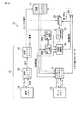
図1は、第1の実施形態に係るプロセッサ11を示している。このプロセッサ11は、例えば命令メモリ12、命令フェッチユニット13、命令デコードユニット14を含むベースとなるプロセッサパイプライン15と、SIMD演算器16と、複数の汎用レジスタを含む汎用レジスタファイル17と、メモリアクセスユニット18と、データメモリ19と、並べ替え回路20と、パターン選択回路21と、複数のパターンレジスタ22と、セレクタ23、24を具備している。(First embodiment)
FIG. 1 shows a
前記命令メモリ12は、複数の命令を記憶している。この命令は、後述するように、処理内容を示すオペランドコード、汎用レジスタを指示するためのソースレジスタ番号、デスティネーションレジスタ番号、及びパターンレジスタ番号等を含んでいる。命令フェッチユニット13は、命令メモリ12に接続され、図示せぬプログラムカウンタから出力されるアドレスに従って、命令メモリ12から実行すべき命令を取り出す。命令デコードユニット14は、命令フェッチユニット13と、SIMD演算器16と、汎用レジスタファイル17と、メモリアクセスユニット18と、並べ替え回路20と、パターン選択回路21と、複数のパターンレジスタ22に接続されている。命令デコードユニット14は、命令フェッチユニット13から供給される命令をデコードし、デコード結果として処理内容を示すデータと、レジスタ番号と、並べ方のパターン番号を出力する。命令デコードユニット14から出力される処理内容を示すデータは、SIMD演算器16と、メモリアクセスユニット18と、並べ替え回路20に供給される。また、レジスタ番号は汎用レジスタファイル17に供給され、パターン番号(レジスタ番号)はパターン選択回路21、パターンレジスタ22に供給される。 The
汎用レジスタファイル17は、例えば64ビット長(8バイト/4ハーフワード/2ワード)を有する例えば32個の汎用レジスタにより構成され、並列演算用のデータや並べ替え用のパターンデータなどを格納する。汎用レジスタファイル17は、SIMD演算器16と、メモリアクセスユニット18と、並べ替え回路20に接続されている。汎用レジスタファイル17は、命令デコードユニット14からレジスタ番号が供給されると、レジスタ番号に対応するレジスタに格納されたデータをSIMD演算器16と、メモリアクセスユニット18と、並べ替え回路20に供給する。 The general-
メモリアクセスユニット18は、データメモリ19に接続され、前記処理内容を示すデータに従ってデータメモリ19からデータを読み出したり、データメモリ19にデータを書き込んだりする。データメモリ19は、演算に必要なデータや後述するデータの並べ替えパターンを示すパターンデータ等が格納される。 The
パターンレジスタ22は、例えば4個の32ビット長のレジスタにより構成されている。パターンレジスタ22は、複数のパターンデータを保持する。パターンレジスタ22は、パターン選択回路21に接続されている。パターン選択回路21は、命令デコードユニット14から供給されるパターン番号に従ってパターンレジスタ21に保持されている並べ替えパターンデータを選択し、並べ替え回路20に供給する。 The
並べ替え回路20は、供給されたパターンデータに従って、汎用レジスタファイル17から供給されたデータを並べ替える。並べ変え回路20は、セレクタ23の一方入力端に接続されている。このセレクタ23の他方入力端は、SIMD演算器16の出力端に接続されている。セレクタ23の出力端は、セレクタ24の一方入力端に接続されている。セレクタ24の他方入力端は、メモリアクセスユニット18の出力端に接続されている。セレクタ24の出力端は汎用レジスタファイル17に接続されている。前記SIMD演算器16、メモリアクセスユニット18、並べ変え回路20の動作結果は、セレクタ23、24を介して汎用レジスタファイル17に供給される。 The
図2(a)(b)(c)は、図1に示すプロセッサで実行されるデータ並べ替え命令のフォーマットを示している。各命令は、例えばオペレーションコード(OPCODE)と、2つのソースレジスタ番号(SRC1,SRC2)と、1つのデスティネーションレジスタ番号(DEST)と、パターンレジスタの番号(PT)5つのビットフィールドにより構成されている。 2A, 2B, and 2C show the format of the data rearrangement instruction executed by the processor shown in FIG. Each instruction is composed of, for example, an operation code (OPCODE), two source register numbers (SRC1, SRC2), one destination register number (DEST), and a pattern register number (PT) five bit fields. Yes.
各命令において、MAS.x(x=B、又はH、又はW)は、並べ替え(MAS:merge and sort)命令であることを示すオペレーションコードであり、Bはバイト単位、Hはハーフワード単位、Wはワード単位の並べ替えを示している。SRC1、SRC2は、2つのソースレジスタ番号であり、具体的には、汎用レジスタ番号である。DESTは、1つのデスティネーションレジスタ番号であり、具体的には、汎用レジスタ番号である。PTは、並べ替えのパターンデータ指示する番号である。具体的には、並べ替えの最小単位であるバイト単位の場合、PTはパターンレジスタの番号であり、最小単位の2倍のビット幅の単位であるハーフワード単位の場合、PTはパターンレジスタを2分割した領域の番号である。さらに、最小単位のn倍(但し、nは2のべき乗の数字)のビット幅の単位であるワード単位の場合、PTはパターンレジスタをn分割又はn以上の領域に分割したいずれかの領域の番号である。 In each instruction, MAS. x (x = B, H, or W) is an operation code indicating a sort (MAS: merge and sort) instruction, where B is a byte unit, H is a halfword unit, and W is a word unit. Shows the sort. SRC1 and SRC2 are two source register numbers, specifically, general-purpose register numbers. DEST is one destination register number, specifically a general-purpose register number. PT is a number indicating the pattern data for rearrangement. Specifically, PT is the number of the pattern register in the case of the byte unit that is the minimum unit of rearrangement, and PT is the
図2(a)に示すバイト単位の並べ替えの場合、PTは2ビットにより構成され、図2(b)に示すハーフワード単位の並べ替えの場合、PTは3ビットにより構成され、図2(c)に示すワード単位の並べ替えの場合、PTは5ビットにより構成されている。 In the case of rearrangement in units of bytes shown in FIG. 2 (a), PT is composed of 2 bits, and in the case of rearrangement in units of half words shown in FIG. 2 (b), PT is composed of 3 bits. In the case of rearrangement in units of words shown in c), PT is composed of 5 bits.
図3(a)(b)(c)(d)は、パターンレジスタ22の構成と、パターンレジスタに登録されるパターンデータの形態を示している。パターンレジスタ22には、予め図3(a)(b)(c)(d)に示すような並べ替えパターンが登録される。パターンレジスタ22に登録すべきパターンデータは、前述したようにデータメモリ19に記憶されており、このデータメモリ19に登録されたパターンデータが汎用レジスタファイル17を介してパターンレジスタ22に格納される。 3A, 3B, 3C, and 3D show the configuration of the pattern register 22 and the form of pattern data registered in the pattern register. A rearrangement pattern as shown in FIGS. 3A, 3B, 3C, and 3D is registered in the pattern register 22 in advance. The pattern data to be registered in the pattern register 22 is stored in the
図3(a)は、バイト単位での並べ替え(MAS.B)の場合を示している。この場合、1個のデスティネーションレジスタ中の8バイトのそれぞれに、2個のソースレジスタのデータを並べ替えてコピーする必要がある。すなわち、16バイトのデータから8バイトのデータを選択するため、4ビットを必要とする。したがって、合計8×4=32ビット、1つのパターンレジスタ分のビット数を必要とする。各1バイト(4ビット)のデータが対応するソースレジスタのデータに対応される。このため、バイト単位での並べ替えの場合、32ビット×4個のパターンレジスタに最大4種類までパターンデータを登録することができる。この4種類のパターンデータは、図2(a)に示す2ビットのパターンレジスタ番号PTにより選択される。 FIG. 3A shows the case of rearrangement in units of bytes (MAS.B). In this case, it is necessary to rearrange and copy the data of the two source registers to each of 8 bytes in one destination register. That is, 4 bits are required to select 8-byte data from 16-byte data. Therefore, a total of 8 × 4 = 32 bits and the number of bits for one pattern register are required. Each 1-byte (4-bit) data corresponds to the data of the corresponding source register. For this reason, in the case of rearrangement in units of bytes, up to four types of pattern data can be registered in a 32-bit × 4 pattern register. These four types of pattern data are selected by a 2-bit pattern register number PT shown in FIG.
図3(b)は、ハーフワード単位での並べ替え(MAS.H)の場合を示している。この場合、1個のデスティネーションレジスタ中の4ハーフワードのそれぞれに、2個のソースレジスタのデータを並べ替えてコピーする必要がある。すなわち、8ハーフワードのデータから4ハーフワードのデータを選択するため、選択に3ビットを必要とする。したがって、合計4×3=12ビットを必要とする。図3(b)に示すHW0〜HW3は3ビットであり、各HW0〜HW3に未使用の1ビットが付加されている。このため、合計16ビットであり、1つのパターンレジスタの2分の1の領域に対応する。したがって、データの区切りを考慮すると、図3(b)に示すように、ハーフワード単位での並べ替えの場合、パターンデータは、最大8種類まで登録することが可能である。この8種類のパターンデータは、図2(b)に示す3ビットのパターンレジスタ番号PTにより選択される。 FIG. 3B shows the case of rearrangement in units of half words (MAS.H). In this case, it is necessary to rearrange and copy the data of the two source registers to each of the four halfwords in one destination register. That is, in order to select 4 halfword data from 8 halfword data, 3 bits are required for selection. Therefore, a total of 4 × 3 = 12 bits is required. HW0 to HW3 shown in FIG. 3B is 3 bits, and 1 unused bit is added to each of HW0 to HW3. Therefore, the total is 16 bits, which corresponds to a half area of one pattern register. Therefore, in consideration of data delimiters, as shown in FIG. 3B, in the case of rearrangement in units of half words, it is possible to register up to eight types of pattern data. The eight types of pattern data are selected by a 3-bit pattern register number PT shown in FIG.
図3(c)は、ワード単位での並べ替え(MAS.W)の場合を示している。この場合、1個のデスティネーションレジスタ中の2ワードのそれぞれに、2個のソースレジスタのデータをコピーする必要がある。すなわち、4ワードデータから2ワードのデータを選択するため、選択に2ビットを必要とする。したがって、2×2=4ビットを必要とする。このため、1つのパターンレジスタの8分の1の領域に対応する。したがって、データの区切りを考慮すると、図3(c)に示すように、ワード単位での並べ替えの場合、パターンデータは、最大32種類まで登録することが可能である。この32種類のパターンデータは、図2(c)に示す5ビットのパターンレジスタ番号PTにより選択される。 FIG. 3C shows a case of rearrangement in units of words (MAS.W). In this case, it is necessary to copy data of two source registers to each of two words in one destination register. That is, in order to select 2-word data from 4-word data, 2 bits are required for selection. Therefore, 2 × 2 = 4 bits are required. For this reason, it corresponds to one-eighth area of one pattern register. Therefore, in consideration of data delimiters, as shown in FIG. 3C, in the case of rearrangement in units of words, it is possible to register up to 32 types of pattern data. The 32 types of pattern data are selected by a 5-bit pattern register number PT shown in FIG.
また、図3(d)は、上記バイト単位、ハーフワード単位、ワード単位の並べ替えパターンを混在させた場合を示している。このような構成とすることも可能である。 FIG. 3 (d) shows a case where rearrangement patterns in byte units, half word units, and word units are mixed. Such a configuration is also possible.
パターンレジスタ22に対するパターンデータの登録は、例えば次のようにして行なわれる。データメモリ19は、データの並べ替えに必要な複数のパターンデータを記憶している。このパターンデータは、上記のように、バイト単位、ハーフワード単位、及びワード単位で構成されている。データメモリ19に記憶されたパターンデータは、例えば下記の命令1、命令2に従って読み出され、汎用レジスタファイル17に転送され、パターンレジスタ22に格納される。 Registration of pattern data in the pattern register 22 is performed, for example, as follows. The
命令1:lw $1,($2)
命令2:mv PT0,$1
すなわち、先ず、命令フェッチユニット13はアドレスを指定して命令メモリ12内の命令1(ロードワード命令)を読み出す。この読み出された命令1は、命令デコードユニット14によりデコードされる。このデコード結果は、メモリアクセスユニット18、汎用レジスタファイル17、パターンレジスタ22に供給される。汎用レジスタファイル17は、デコード結果に従って、汎用レジスタ$2のデータを読み出し、メモリアクセスユニット18に送る。メモリアクセスユニット18は、汎用レジスタ$2のデータをアドレスとしてデータメモリ19からパターンデータを読み出す。この読み出されたパターンデータは、セレクタ24を介して汎用レジスタファイル17の指定された汎用レジスタ$1に格納される。Instruction 1: lw $ 1, ($ 2)
Instruction 2: mv PT0, $ 1
That is, first, the instruction fetch
次に、命令フェッチユニット13はアドレスを指定して命令メモリ12から命令2(ムーブ命令)を読み出す。命令デコードユニット14は、この読み出された命令2をデコードする。汎用レジスタファイル17は、デコード結果に従って、汎用レジスタ$1のデータを読み出し、SIMD演算器16に送る。SIMD演算器12は何も行わず、SIMD演算器12をスルーしたデータは、セレクタ23を介して指定されたパターンレジスタPT0に書き込まれる。 Next, the instruction fetch
上記のような命令1、命令2を繰り返すことにより、パターンレジスタPT0〜PT3にパターンデータが格納される。 By repeating the
尚、パターンレジスタ22へのパターンデータの格納方法は、上記例に限定されるものではなく、変形可能である。 The method for storing pattern data in the pattern register 22 is not limited to the above example, and can be modified.
図4は、並び替え命令の一例と、この命令に対応した並べ替え処理の例を示している。図4において、並び替え命令 MAS.H $0,$1,$2,PT0は、ハーフワード単位で、4つのパターンレジスタのうちの0番(PT0)に保持されたパターンデータに従って、汎用レジスタ$1と$2のデータを並べ替えて汎用レジスタ$0に格納するという命令である。 FIG. 4 shows an example of a rearrangement instruction and an example of rearrangement processing corresponding to this instruction. In FIG. 4, the rearrangement instruction MAS. H $ 0, $ 1, $ 2, PT0 rearrange the data in general-purpose registers $ 1 and $ 2 in halfword units according to the pattern data held in number 0 (PT0) of the four pattern registers Is stored in the general-purpose register $ 0.
上記並び替え命令MAS.Hが発行されると、データ並べ替え回路20は、汎用レジスタファイル17の2つの汎用レジスタ$1、$2からデータを読み出す。さらに、命令中のパターンレジスタの番号PT0により指定されたパターンレジスタPT0から並べ替えパターンを示すパターンデータを読み出す。この後、パターンデータに従って汎用レジスタ$1、$2から読み出されたデータを並べ替える。この並べ替えられたデータは、セレクタ23、24を介して汎用レジスタ17に転送され格納される。この後、SIMD演算命令が発行されると、前記並び替えられたデータが汎用レジスタファイル17から読み出され、SIMD演算器16により演算される。この演算結果は、セレクタ23,24を介して選択された汎用レジスタに格納される。このようにして、データの並べ替え、及びSIMD演算が実行される。 The rearrangement instruction MAS. When H is issued, the
上記第1の実施形態によれば、パターンレジスタ22は予め並べ替えパターンを示すパターンデータを登録し、パターン選択回路21は、並べ替え命令に含まれるパターンレジスタ番号PTに従って並べ替えパターンを選択し、並べ替え回路20は、選択された並べ替えパターンに従って汎用レジスタの内容を並べ替えている。このため、第1の実施形態によれば、前記プログラム(1)に示した12命令で行っていた並べ替え処理を、図4に示す1命令により、完了することができる。したがって、データの並び替えに要する時間を大幅に短縮することができ、SIMD演算回路16の演算速度を向上させることができる。 According to the first embodiment, the pattern register 22 registers pattern data indicating the rearrangement pattern in advance, and the
また、複数のパターンレジスタ22に複数のパターンデータを記憶させることにより、並べ替え命令の増加を抑制して、所要のパターンにデータを並べ替えることができる。 In addition, by storing a plurality of pattern data in the plurality of pattern registers 22, it is possible to suppress the increase in the rearrangement command and rearrange the data into a required pattern.
しかも、並べ替えがバイト単位、ハーフワード単位、ワード単位の場合のように、複数の単位がある場合において、各単位に応じてパターンレジスタ22に記憶されるパターンデータの数を変えている。このため、パターンレジスタ22の記憶領域を有効に活用することが可能である。 In addition, when there are a plurality of units such as rearrangement in byte units, half word units, and word units, the number of pattern data stored in the pattern register 22 is changed according to each unit. For this reason, the storage area of the pattern register 22 can be used effectively.
尚、図3(b)に示すようにパターンレジスタ内に未使用の領域が生じた場合、その未使用の領域に例えばオプション機能を設定することも可能である。 When an unused area is generated in the pattern register as shown in FIG. 3B, for example, an optional function can be set in the unused area.
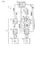
(第2の実施形態)
図5は、第2の実施形態に係るプロセッサを示している。以下の各実施形態において、図1と同一部分には、同一符号を付し、異なる部分についてのみ説明する。(Second Embodiment)
FIG. 5 shows a processor according to the second embodiment. In the following embodiments, the same parts as those in FIG. 1 are denoted by the same reference numerals, and only different parts will be described.
上記第1の実施形態において、SIMD演算器16と並べ替え回路20は並列に配置され、並べ替え回路20は、SIMD演算器16から独立してデータの並べ替え処理を行なった。 In the first embodiment, the SIMD
これに対して、第2の実施形態のプロセッサは、図5に示すように、SIMD演算器16と並べ替え回路20が直列に配置されている。SIMD演算器16と並べ替え回路20は、並べ替え命令を含む1つのSIMD演算命令により動作される。すなわち、1つの命令に従ってSIMD演算器16は、汎用レジスタのデータをSIMD演算し、並べ替え回路20は、SIMD演算器16の出力データを並べ替える。並べ替え回路20の出力データは、SIMD演算命令の結果として汎用レジスタファイル17の指定された汎用レジスタに格納される。 On the other hand, in the processor according to the second embodiment, as shown in FIG. 5, the
図6(a)(b)(c)は、図5に示すプロセッサで実行されるデータ並べ替え命令を含むSIMD命令のフォーマットの例を示している。 FIGS. 6A, 6B, and 6C show examples of SIMD instruction formats including data rearrangement instructions executed by the processor shown in FIG.
各命令は、オペレーションコード(OPCODE)と、パターンレジスタ番号(PT)、又はパターン番号(IPT)と、2個のソースレジスタ番号(SRC1、SRC2)と、デスティネーションレジスタ番号(DEST)の5つのビットフィールドにより構成されている。 Each instruction has five bits: an operation code (OPCODE), a pattern register number (PT), or a pattern number (IPT), two source register numbers (SRC1, SRC2), and a destination register number (DEST). It consists of fields.
すなわち、図6(a)(b)(c)において、演算内容を示すオペレーションコードADDSRT.x(x=B、又はH、又はW)は、SIMDの加算演算と並べ替えを行い、演算結果をデスティネーションレジスタに格納する命令を示しており、Bはバイト単位、Hはハーフワード単位、Wはワード単位であることを示している。図6(a)(b)に示すパターンレジスタ番号PTは、バイト単位及びハーフワード単位の演算結果を並べ替える際に使用するパターンレジスタ番号を示している。図6(c)に示すパターン番号IPTは、ワード単位の演算結果を並べ替えるための後述する4種類のパターンのうちのいずれかを指定する番号である。SRC1、SRC2は、処理に必要な2個のソースレジスタ番号、すなわち、汎用レジスタの番号を示し、DESTは、演算結果が格納されるデスティネーションレジスタ番号、すなわち、汎用レジスタの番号を示している。 That is, in FIGS. 6A, 6B and 6C, the operation code ADDDSRT. x (x = B, H, or W) indicates an instruction that performs addition and rearrangement of SIMD and stores the operation result in the destination register, where B is a byte unit, H is a halfword unit, W indicates a word unit. Pattern register numbers PT shown in FIGS. 6A and 6B indicate pattern register numbers used when rearranging the operation results in byte units and half word units. The pattern number IPT shown in FIG. 6C is a number that designates one of four types of patterns to be described later for rearranging the calculation results in word units. SRC1 and SRC2 indicate two source register numbers necessary for processing, that is, general-purpose register numbers, and DEST indicates a destination register number in which an operation result is stored, that is, a general-purpose register number.
尚、ソースレジスタの個数は、2個に限定されるものではなく、命令のビット幅に収まれば2個以上であってもよい。 Note that the number of source registers is not limited to two, and may be two or more as long as it fits within the bit width of the instruction.
図7(a)(b)(d)は、パターンレジスタ22の構成と並べ替えパターンの例を示している。 7A, 7B, and 7D show examples of the configuration of the pattern register 22 and the rearrangement pattern.
図7(a)は、バイト単位での並び替え(ADDSRT.B)の例を示している。この場合、SIMD演算器16の演算結果は、図示せぬレジスタに記憶されている。このため、1個のデスティネーションレジスタ中の8バイトそれぞれに、SIMD演算器16の1個のレジスタの8バイトのデータをコピーする必要がある。すなわち、8バイトのデータを選択するため、3ビットを必要とする。したがって、合計8×3=24ビットを必要とする。データの区切りを考慮すると、この場合、最大4種類までパターンデータを登録することが可能である。この4種類のパターンデータは、図6(a)に示す2ビットのパターンレジスタ番号PTにより選択される。 FIG. 7A shows an example of rearrangement in units of bytes (ADDSRT.B). In this case, the calculation result of the
図7(b)は、ハーフワード単位での並び替え(ADDSRT.H)の例を示している。この場合、1個のデスティネーションレジスタ中の4ハーフワードそれぞれに、SIMD演算器16の1個のレジスタの4ハーフワードデータをコピーする必要がある。すなわち、4ハーフワードのデータを選択するために2ビットを必要とする。したがって、合計4×2=8ビットを必要とする。この場合、図7(b)に示すように、最大16種類のパターンデータを登録することが可能である。この16種類のパターンデータは、図6(b)に示す4ビットパターンレジスタ番号PTにより選択される。 FIG. 7B shows an example of rearrangement in units of half words (ADDSRT.H). In this case, it is necessary to copy 4 halfword data of one register of the
図7(c)は、ワード単位での並び替え(ADDSRT.H)の例を示している。この場合、パターンデータは図7(c)に示す4通りしか存在しない。すなわち、SIMD演算器16の演算結果{Word0,Word1}を並べ替えるパターンは、4種類しかない。このため、パターンデータを選択するために6ビットのパターンレジスタ番号PTのフィールドを用意する代わりに、図6(c)に示すように、直接パターンを指定する専用の2ビットのフィールドIPTを用意している。 FIG. 7C shows an example of rearrangement in units of words (ADDDSRT.H). In this case, there are only four types of pattern data as shown in FIG. That is, there are only four patterns for rearranging the calculation results {Word0, Word1} of the
また、図7(d)は、上記バイト単位、ハーフワード単位、ワード単位の並べ替えパターンを混在させた場合を示している。このような構成とすることも可能である。 FIG. 7D shows a case where the rearrangement patterns in byte units, half word units, and word units are mixed. Such a configuration is also possible.
上記構成において、図8に示すように、例えばADDSRT.H命令及びADD.H命令が順次発行された場合の動作について説明する。先ず、ADDSRT.H命令が発行されると、SIMD演算器16は、汎用レジスタファイル17から指定された汎用レジスタ$1、$2のデータを読み出し、加算する。並べ替え回路20は、加算結果を並べ替えてデスティネーションレジスタ$4に格納する。すなわち、並べ替え回路20は、命令中で指定されたパターンレジスタ番号PT0に対応するパターンレジスタのデータを読み出して加算結果を並べ替える。 In the above configuration, as shown in FIG. H instruction and ADD. The operation when H instructions are sequentially issued will be described. First, ADDDSRT. When the H instruction is issued, the SIMD
この後、ADD.H命令が発行されると、SIMD演算器16は、汎用レジスタファイル17から指定された汎用レジスタ$3、$4のデータを読み出し、加算する。このとき、並べ替え回路20は、何ら処理せずにスルーし、加算結果は、デスティネーションレジスタ$0に格納される。 After this, ADD. When the H instruction is issued, the SIMD
上記第2の実施形態によれば、予め複数のパターンレジスタ22に複数のパターンデータを記憶し、又は命令内にパターン番号IPTを設定している。このため、データの並べ替えに要する命令数を削減して、所要の並べ替えを実行することができる。 According to the second embodiment, a plurality of pattern data is stored in advance in the plurality of pattern registers 22, or the pattern number IPT is set in the instruction. For this reason, it is possible to reduce the number of instructions required for data rearrangement and execute the required rearrangement.
しかも、SIMD演算器16と並べ替え回路20を直列に配置し、SIMD演算器16による演算の後に、予め記憶されたパターンレジスタ22にパターンデータ、又は命令内のパターン番号IPTに基づき、並べ替え回路20で並べ替えを実行している。このため、SIMD演算とデータの並べ替えを1つの命令により実行することができる。したがって、図9に示すような、従来10命令を必要とした処理を2命令で完了することができ、演算速度を向上することができる。 In addition, the SIMD
(第3の実施形態)
図10は、第3の実施形態に係るプロセッサを示している。第2の実施形態は、SIMD演算後、データの並べ替えを行った。これに対して、第3の実施形態は、SIMD演算前に、2個のソースレジスタのデータをそれぞれ並べ替える構成とされている。(Third embodiment)
FIG. 10 shows a processor according to the third embodiment. In the second embodiment, the data is rearranged after the SIMD calculation. On the other hand, the third embodiment is configured to rearrange the data of the two source registers before the SIMD calculation.
すなわち、2個の並べ替え回路20a,20bの入力端は、汎用レジスタファイル17に接続されている。これら並べ替え回路20a,20bの出力端は、SIMD演算器16に接続されている。パターン選択回路21の出力端は、並べ替え回路20a,20bに接続されている。 That is, the input terminals of the two
図11(a)(b)(c)は、第3の実施形態の命令フォーマットの一例を示している。図11(a)(b)(c)に示す命令は、オペレーションコード(OPCODE)、パターンレジスタ番号(PT1、PT2)、ワード単位用パターン番号(IPT1、IPT2)、ソースレジスタ番号(SRC1、SRC2)、デスティネーションレジスタ番号DESTを含む6個のビットフィールドを有している。 FIGS. 11A, 11B, and 11C show examples of the instruction format of the third embodiment. The instructions shown in FIGS. 11A, 11B, and 11C are an operation code (OPCODE), pattern register numbers (PT1, PT2), word unit pattern numbers (IPT1, IPT2), and source register numbers (SRC1, SRC2). And 6 bit fields including the destination register number DEST.
オペレーションコードSRTADD.x(x=B、又はH、又はW)は、並べ替え後、SIMDの加算演算を行うことを示している。2ビット又は4ビットのパターンレジスタ番号PT1、PT2は、それぞれソースレジスタSRC1、SRC2に対応したパターンレジスタを指定する。ワード単位用パターン番号IPT1、IPT2は、それぞれソースレジスタSRC1、SRC2に対応したパターンレジスタを指定する。SRC1、SRC2は、処理に必要な2個のソースレジスタ番号、すなわち、汎用レジスタの番号を示し、DESTは、演算結果が格納されるデスティネーションレジスタ番号、すなわち、汎用レジスタの番号を示している。 Operation code SRTADD. x (x = B, H, or W) indicates that the SIMD addition operation is performed after the rearrangement. The 2-bit or 4-bit pattern register numbers PT1 and PT2 designate pattern registers corresponding to the source registers SRC1 and SRC2, respectively. The word unit pattern numbers IPT1 and IPT2 specify pattern registers corresponding to the source registers SRC1 and SRC2, respectively. SRC1 and SRC2 indicate two source register numbers necessary for processing, that is, general-purpose register numbers, and DEST indicates a destination register number in which an operation result is stored, that is, a general-purpose register number.
次に、具体的な命令の一例を示す。 Next, an example of a specific command is shown.
SRTADD.H $0,$1,$2,PT1,PT2
上記命令を実行する場合、並べ替え回路20a,20bは、ソースレジスタ$1、$2から読み出したデータを、パターンレジスタPT1、PT2に記憶されたパターンデータに従ってそれぞれ並べ替える。この後、SIMD演算器16は、並べ替え回路20a,20bにより並べ替えられた両データを加算してデスティネーションレジスタ$0に格納する。SRTADD. H $ 0, $ 1, $ 2, PT1, PT2
When executing the above instruction, the
上記第3の実施形態によれば、SIMD演算器16の前段に並べ替え回路20a,20bを設け、これら並べ替え回路20a,20bにより2つのソースレジスタから読み出されたデータをパターンレジスタ22に記憶されたパターンデータに従って並べ替え、この後、SIMD演算を実行している。このため、第3の実施形態によっても第2の実施形態と同様に、データの並べ替えに要する命令数を削減して、所要の並べ替えを実行することが可能である。 According to the third embodiment, the
しかも、データの並べ替えとSIMD演算を1つの命令により実行することができるため、演算速度を向上することが可能である。 In addition, since data rearrangement and SIMD calculation can be executed by one instruction, the calculation speed can be improved.
(第4の実施形態)
図12は、第4の実施形態に係るプロセッサを示している。第4の実施形態は、第1の実施形態を変形したものである。第1の実施形態は、専用のパターンレジスタ22を設けていた。これに対して、第4の実施形態は、専用のパターンレジスタを設けず、図12に示すように、汎用レジスタファイル17に並べ替えパターンを登録し、ソースレジスタと同様にパターンデータを読み出して使用するという構成である。すなわち、汎用レジスタファイル17がパターンレジスタを兼用している。このため、パターン選択回路21は、汎用レジスタファイル17に接続されている。(Fourth embodiment)
FIG. 12 shows a processor according to the fourth embodiment. The fourth embodiment is a modification of the first embodiment. In the first embodiment, a dedicated pattern register 22 is provided. On the other hand, in the fourth embodiment, a dedicated pattern register is not provided, and as shown in FIG. 12, a rearrangement pattern is registered in the general-
図13(a)(b)(c)は、この構成のプロセッサで実行される命令フォーマットの一例を示している。各命令は、オペレーションコード(OPCODE)と、2つのソースレジスタ番号(SRC1,SRC2)と、1つのデスティネーションレジスタ番号(DEST)と、パターンレジスタの番号(PT)と、パターンレジスタのどの部分を使用するかを示すビットフィールド(PL)という6つのビットフィールドにより構成されている。 FIGS. 13A, 13B and 13C show an example of an instruction format executed by the processor having this configuration. Each instruction uses an operation code (OPCODE), two source register numbers (SRC1, SRC2), one destination register number (DEST), a pattern register number (PT), and which part of the pattern register It is composed of six bit fields called bit fields (PL) indicating whether or not to perform.
第4の実施形態によれば、第1の実施形態に比べて命令において、パターンを選択するために必要とするビット数が多くなり、命令長が長くなる。しかし、パターンレジスタを必要としないため回路構成を簡単化できる。 According to the fourth embodiment, as compared with the first embodiment, the number of bits required for selecting a pattern is increased in the instruction, and the instruction length is increased. However, since no pattern register is required, the circuit configuration can be simplified.
また、汎用レジスタファイル17を用いることにより、4つのレジスタからなるパターンレジスタを用いる場合に比べて、より多くのパターンデータを格納することができ、多くのパターンデータを使用することができる。 Further, by using the general-
尚、第4の実施形態を、第2、第3の実施形態と組み合わせて構成することも可能である。 The fourth embodiment can be configured in combination with the second and third embodiments.
(第5の実施形態)
図14は、第5の実施形態に係るプロセッサを示している。第5の実施形態は、第1乃至第4の実施形態と異なり、並べ替え回路が並べ替え以外にビット反転を行う機能を有している。(Fifth embodiment)
FIG. 14 shows a processor according to the fifth embodiment. In the fifth embodiment, unlike the first to fourth embodiments, the rearrangement circuit has a function of performing bit inversion in addition to rearrangement.
すなわち、図14において、例えばSIMD演算器16に並列に並べ替え及び反転回路30が配置されている。この並べ替え及び反転回路30は、例えばハーフワード単位、及びワード単位で並べ替えを行う際、パターンレジスタのパターンデータ以外のビットを用いて指定された反転指示に基づき、ビット反転を実行する。すなわち、例えば後述する図15(b)に示すハーフワード単位の場合、未使用の1ビットが反転指示ビットとして使用される。 That is, in FIG. 14, for example, a rearrangement and
図15(a)(b)(c)(d)は、パターンレジスタの構成とパターンデータの登録の形態を示している。 FIGS. 15A, 15B, 15C, and 15D show the configuration of the pattern register and the pattern data registration mode.
図15(a)に示すMAS.B、及び図15(d)に示すパターンデータを混在して登録する例は、第1の実施形態と同様である。 The MAS. An example in which B and the pattern data shown in FIG. 15D are registered together is the same as in the first embodiment.
図15(b)に示すMAS.Hの場合、1ハーフワードにつき1ビットの未使用ビットが存在する。このため、この1ビットを反転指定ビットとして利用している。この反転指定ビットが例えば“1”に設定されている場合、ビット反転動作が実行される。 The MAS. In the case of H, there is one unused bit per halfword. For this reason, this 1 bit is used as an inversion designation bit. For example, when the inversion designation bit is set to “1”, a bit inversion operation is performed.
図15(c)に示すMAS.Wの場合、第1の実施形態と同様の形態にすることも可能であるが、図15(c)では、登録できるパターンデータの種類を16種類に削減し、余ったビットを反転指定ビットとして利用している。この反転指定ビットが例えば“1”に設定されている場合、ビット反転動作が実行される。 The MAS. In the case of W, it is possible to adopt the same form as in the first embodiment. However, in FIG. 15C, the types of pattern data that can be registered are reduced to 16, and the remaining bits are used as inversion designated bits. We are using. For example, when the inversion designation bit is set to “1”, a bit inversion operation is performed.
図16(a)(b)(c)は、第5の実施形態に係る命令フォーマットの一例を示している。図16(a)(b)(c)に示す命令は、オペレーションコード(OPCODE)、パターンレジスタ番号(PT)、ソースレジスタ番号(SRC1、SRC2)、デスティネーションレジスタ番号DESTを含む5個のビットフィールドを有している。 FIGS. 16A, 16B, and 16C show an example of an instruction format according to the fifth embodiment. The instructions shown in FIGS. 16A, 16B, and 16C are five bit fields including an operation code (OPCODE), a pattern register number (PT), a source register number (SRC1, SRC2), and a destination register number DEST. have.
オペレーションコードMASI.x(x=B、又はH、又はW)は、並べ替え及びビット反転を行うことを示している。2ビット乃至4ビットのパターンレジスタ番号PTは、パターンレジスタを指定する。それぞれソースレジスタSRC1、SRC2に対応したパターンレジスタを指定する。SRC1、SRC2は、処理に必要な2個のソースレジスタ番号、すなわち、汎用レジスタの番号を示し、DESTは、演算結果が格納されるデスティネーションレジスタ番号、すなわち、汎用レジスタの番号を示している。 Operation code MASI. x (x = B, H, or W) indicates that rearrangement and bit inversion are performed. The 2-bit to 4-bit pattern register number PT designates a pattern register. Designate pattern registers corresponding to the source registers SRC1 and SRC2, respectively. SRC1 and SRC2 indicate two source register numbers necessary for processing, that is, general-purpose register numbers, and DEST indicates a destination register number in which an operation result is stored, that is, a general-purpose register number.
上記構成において、MAS.x(H、又はW)命令が発行されると、並べ替え及び反転回路30は、汎用レジスタファイルから2個のソースレジスタのデータを読み出し、命令中のパターンレジスタ番号PTで指定されたパターンレジスタからパターンデータを読み出してデータの並べ替えを行う。その際、パターンデータの反転指示ビットが“1”に設定されている場合、この反転指示ビットが設定されたデータのみ、並べ替えと同時にビットが反転される。このように、並べ替え及びビット反転後のデータは、指定されたデスティネーションレジスタに格納される。 In the above configuration, MAS. When the x (H or W) instruction is issued, the rearrangement and
上記第5の実施形態によれば、並べ替え及び反転回路30は、データの並べ替えとビット反転機能を有し、パターンデータに含まれる反転指示データにより、並べ替えられたデータのビットを反転する。このため、データの並べ替えとビット反転を1命令で実行することができるため、命令数を削減することが可能である。したがって、演算速度を高速化することができる。 According to the fifth embodiment, the rearrangement and
尚、第5の実施形態は、並べ替えと反転動作を行ったが、これに限定されるものではなく、並べ替えに加えて、反転動作以外のオプション処理を設定することも可能である。 In the fifth embodiment, the rearrangement and inversion operations are performed. However, the present invention is not limited to this, and optional processing other than the inversion operation can be set in addition to the rearrangement.
また、第5の実施形態の並べ替え及び反転回路30(反転に限定されない)を、第2、第3、第4の実施形態のような構成に適用することも可能である。 Further, the rearrangement and inversion circuit 30 (not limited to inversion) of the fifth embodiment can be applied to the configurations of the second, third, and fourth embodiments.
その他、本発明は、上記各実施形態に限定されるものではなく、発明の要旨を変えない範囲において、種々変形実施可能なことは勿論である。 In addition, the present invention is not limited to the above-described embodiments, and various modifications can be made without departing from the scope of the invention.
16…SIMD演算器、17…汎用レジスタファイル、20、20a、20b…並べ替え回路、21…パターン選択回路、22…パターンレジスタ、30…並べ替え及び反転回路。 DESCRIPTION OF
Claims (4)
Translated fromJapanese前記データの並べ替えを示す複数のパターンデータを、最小のビット幅の単位、最小のビット幅の2倍のビット幅の単位、最小単位のn倍(但し、nは2のべき乗の数字)のビット幅の単位のうちの1つ、又はこれらの組み合わせにより記憶する複数のパターンレジスタと、
命令に含まれる指示データに従って前記複数のパターンレジスタに記憶された複数のパターンデータのうちの1つを選択する選択回路と、
前記選択回路により選択されたパターンデータに従って前記並列演算用のデータを並べ替える並べ替え回路とを具備し、
前記選択回路は、前記並列演算用データの並べ替えを行う最小のビット幅の単位で並べ替える場合はパターンレジスタ全体を選択し、最小単位の2倍のビット幅の単位で並べ替える場合はパターンレジスタを2分割したいずれかの領域を選択し、最小単位のn倍(但し、nは2のべき乗の数字)のビット幅の単位で並べ替える場合はパターンレジスタをn分割又はn以上の領域に分割したいずれかの領域を選択することを特徴とする演算装置。Multiple general-purpose registers to store data for parallel operations;
A plurality of pattern data indicating the rearrangement of data is represented by a minimum bit width unit, a bit width unit twice the minimum bit width, and n times the minimum unit (where n is a power of 2). A plurality of pattern registers storing one of the bit width units, or a combination thereof;
A selection circuit for selecting one of a plurality of pattern data stored in the plurality of pattern registers according to instruction data included in the instruction;
A rearrangement circuit for rearranging the data for parallel operation according to the pattern data selected by the selection circuit;
The selection circuit selects the entire pattern register when rearranging in the unit of the minimum bit width for rearranging the parallel operation data, and selects the pattern register when rearranging in the unit of the bit width twice the minimum unit. Select one of the areas divided into 2 and divide the pattern register into n or more than n areas when rearranging them in units of a bit width of n times the minimum unit (where n is a power of 2) An arithmetic device characterizedby selecting any one of the regions .
Priority Applications (2)
| Application Number | Priority Date | Filing Date | Title |
|---|---|---|---|
| JP2006292960AJP4686435B2 (en) | 2006-10-27 | 2006-10-27 | Arithmetic unit |
| US11/923,085US8051122B2 (en) | 2006-10-27 | 2007-10-24 | SIMD arithmetic device capable of high-speed computing |
Applications Claiming Priority (1)
| Application Number | Priority Date | Filing Date | Title |
|---|---|---|---|
| JP2006292960AJP4686435B2 (en) | 2006-10-27 | 2006-10-27 | Arithmetic unit |
Publications (2)
| Publication Number | Publication Date |
|---|---|
| JP2008108220A JP2008108220A (en) | 2008-05-08 |
| JP4686435B2true JP4686435B2 (en) | 2011-05-25 |
Family
ID=39441500
Family Applications (1)
| Application Number | Title | Priority Date | Filing Date |
|---|---|---|---|
| JP2006292960AExpired - Fee RelatedJP4686435B2 (en) | 2006-10-27 | 2006-10-27 | Arithmetic unit |
Country Status (2)
| Country | Link |
|---|---|
| US (1) | US8051122B2 (en) |
| JP (1) | JP4686435B2 (en) |
Families Citing this family (7)
| Publication number | Priority date | Publication date | Assignee | Title |
|---|---|---|---|---|
| JPWO2010067522A1 (en)* | 2008-12-11 | 2012-05-17 | 日本電気株式会社 | Arithmetic unit, processor and parallel computing method |
| KR101918464B1 (en)* | 2011-09-14 | 2018-11-15 | 삼성전자 주식회사 | A processor and a swizzle pattern providing apparatus based on a swizzled virtual register |
| CN103999045B (en) | 2011-12-15 | 2017-05-17 | 英特尔公司 | Method for Optimizing Program Loops via Vector Instructions Using Shuffle and Mix Tables |
| WO2014092183A1 (en)* | 2012-12-14 | 2014-06-19 | 日本電気株式会社 | Bit string matching system, method, and program |
| US9977676B2 (en)* | 2013-11-15 | 2018-05-22 | Qualcomm Incorporated | Vector processing engines (VPEs) employing reordering circuitry in data flow paths between execution units and vector data memory to provide in-flight reordering of output vector data stored to vector data memory, and related vector processor systems and methods |
| US9880845B2 (en)* | 2013-11-15 | 2018-01-30 | Qualcomm Incorporated | Vector processing engines (VPEs) employing format conversion circuitry in data flow paths between vector data memory and execution units to provide in-flight format-converting of input vector data to execution units for vector processing operations, and related vector processor systems and methods |
| JP2018022339A (en)* | 2016-08-03 | 2018-02-08 | 富士通株式会社 | Calculation processor and control method of calculation processor |
Family Cites Families (9)
| Publication number | Priority date | Publication date | Assignee | Title |
|---|---|---|---|---|
| JP2001344099A (en) | 2000-05-30 | 2001-12-14 | Canon Inc | Information processing apparatus and information processing method in the apparatus |
| JP3955741B2 (en)* | 2001-04-02 | 2007-08-08 | 株式会社リコー | SIMD type microprocessor having sort function |
| US7631025B2 (en)* | 2001-10-29 | 2009-12-08 | Intel Corporation | Method and apparatus for rearranging data between multiple registers |
| US7272622B2 (en)* | 2001-10-29 | 2007-09-18 | Intel Corporation | Method and apparatus for parallel shift right merge of data |
| US7685212B2 (en)* | 2001-10-29 | 2010-03-23 | Intel Corporation | Fast full search motion estimation with SIMD merge instruction |
| US7818356B2 (en)* | 2001-10-29 | 2010-10-19 | Intel Corporation | Bitstream buffer manipulation with a SIMD merge instruction |
| US20040054877A1 (en)* | 2001-10-29 | 2004-03-18 | Macy William W. | Method and apparatus for shuffling data |
| GB2394571B (en)* | 2002-10-23 | 2005-08-10 | Motorola Inc | Arrangement system and method for vector permutation in single-instruction multiple-data microprocessors |
| JP2006190035A (en)* | 2005-01-05 | 2006-07-20 | Seiko Epson Corp | Computer device and printing device |
- 2006
- 2006-10-27JPJP2006292960Apatent/JP4686435B2/ennot_activeExpired - Fee Related
- 2007
- 2007-10-24USUS11/923,085patent/US8051122B2/ennot_activeExpired - Fee Related
Also Published As
| Publication number | Publication date |
|---|---|
| JP2008108220A (en) | 2008-05-08 |
| US8051122B2 (en) | 2011-11-01 |
| US20080282070A1 (en) | 2008-11-13 |
Similar Documents
| Publication | Publication Date | Title |
|---|---|---|
| US9383999B2 (en) | Conditional compare instruction | |
| KR100267100B1 (en) | Scalable Vector Processor Architecture | |
| US7761693B2 (en) | Data processing apparatus and method for performing arithmetic operations in SIMD data processing | |
| JP4686435B2 (en) | Arithmetic unit | |
| CN109416633B (en) | Apparatus and method for performing rearrangement operation | |
| EP1267256A2 (en) | Conditional execution of instructions with multiple destinations | |
| US20050198473A1 (en) | Multiplexing operations in SIMD processing | |
| JP5559297B2 (en) | Coding hardware end loop information into instructions | |
| KR20110055629A (en) | Providing extended addressing modes in a single instruction multiple data (SIMD) data processor | |
| US9965275B2 (en) | Element size increasing instruction | |
| JP7213095B2 (en) | Vector register access | |
| KR20180035211A (en) | Vector arithmetic instruction | |
| KR20070107814A (en) | Processor and method for grouping dependency instructions into packets | |
| US8604946B2 (en) | Data processing device and data processing method | |
| KR102591988B1 (en) | Vector interleaving in data processing units | |
| WO2010067522A1 (en) | Computation unit, processor, and parallel computation method | |
| CN106610817A (en) | Method for assigning or extending a constant number of bits with a constant extension slot in the same execution packet in a VLIW processor | |
| JP2003241960A (en) | Processor, operation instruction processing method and operation control method in the processor | |
| JP2002073325A (en) | Data processing device and method | |
| JP2004139156A (en) | Arithmetic processor |
Legal Events
| Date | Code | Title | Description |
|---|---|---|---|
| A621 | Written request for application examination | Free format text:JAPANESE INTERMEDIATE CODE: A621 Effective date:20090804 | |
| A977 | Report on retrieval | Free format text:JAPANESE INTERMEDIATE CODE: A971007 Effective date:20101027 | |
| A131 | Notification of reasons for refusal | Free format text:JAPANESE INTERMEDIATE CODE: A131 Effective date:20101102 | |
| A521 | Request for written amendment filed | Free format text:JAPANESE INTERMEDIATE CODE: A523 Effective date:20101222 | |
| TRDD | Decision of grant or rejection written | ||
| A01 | Written decision to grant a patent or to grant a registration (utility model) | Free format text:JAPANESE INTERMEDIATE CODE: A01 Effective date:20110118 | |
| A01 | Written decision to grant a patent or to grant a registration (utility model) | Free format text:JAPANESE INTERMEDIATE CODE: A01 | |
| A61 | First payment of annual fees (during grant procedure) | Free format text:JAPANESE INTERMEDIATE CODE: A61 Effective date:20110214 | |
| FPAY | Renewal fee payment (event date is renewal date of database) | Free format text:PAYMENT UNTIL: 20140218 Year of fee payment:3 | |
| FPAY | Renewal fee payment (event date is renewal date of database) | Free format text:PAYMENT UNTIL: 20140218 Year of fee payment:3 | |
| LAPS | Cancellation because of no payment of annual fees |