JP4683075B2 - Silicon carbide semiconductor device and manufacturing method thereof - Google Patents
Silicon carbide semiconductor device and manufacturing method thereofDownload PDFInfo
- Publication number
- JP4683075B2 JP4683075B2JP2008151370AJP2008151370AJP4683075B2JP 4683075 B2JP4683075 B2JP 4683075B2JP 2008151370 AJP2008151370 AJP 2008151370AJP 2008151370 AJP2008151370 AJP 2008151370AJP 4683075 B2JP4683075 B2JP 4683075B2
- Authority
- JP
- Japan
- Prior art keywords
- layer
- region
- trench
- conductivity type
- type
- Prior art date
- Legal status (The legal status is an assumption and is not a legal conclusion. Google has not performed a legal analysis and makes no representation as to the accuracy of the status listed.)
- Expired - Fee Related
Links
Images


Classifications
- H—ELECTRICITY
- H10—SEMICONDUCTOR DEVICES; ELECTRIC SOLID-STATE DEVICES NOT OTHERWISE PROVIDED FOR
- H10D—INORGANIC ELECTRIC SEMICONDUCTOR DEVICES
- H10D30/00—Field-effect transistors [FET]
- H10D30/60—Insulated-gate field-effect transistors [IGFET]
- H10D30/64—Double-diffused metal-oxide semiconductor [DMOS] FETs
- H10D30/66—Vertical DMOS [VDMOS] FETs
- H10D30/665—Vertical DMOS [VDMOS] FETs having edge termination structures
- H—ELECTRICITY
- H01—ELECTRIC ELEMENTS
- H01L—SEMICONDUCTOR DEVICES NOT COVERED BY CLASS H10
- H01L21/00—Processes or apparatus adapted for the manufacture or treatment of semiconductor or solid state devices or of parts thereof
- H01L21/02—Manufacture or treatment of semiconductor devices or of parts thereof
- H01L21/04—Manufacture or treatment of semiconductor devices or of parts thereof the devices having potential barriers, e.g. a PN junction, depletion layer or carrier concentration layer
- H01L21/0445—Manufacture or treatment of semiconductor devices or of parts thereof the devices having potential barriers, e.g. a PN junction, depletion layer or carrier concentration layer the devices having semiconductor bodies comprising crystalline silicon carbide
- H01L21/0455—Making n or p doped regions or layers, e.g. using diffusion
- H—ELECTRICITY
- H10—SEMICONDUCTOR DEVICES; ELECTRIC SOLID-STATE DEVICES NOT OTHERWISE PROVIDED FOR
- H10D—INORGANIC ELECTRIC SEMICONDUCTOR DEVICES
- H10D12/00—Bipolar devices controlled by the field effect, e.g. insulated-gate bipolar transistors [IGBT]
- H10D12/01—Manufacture or treatment
- H10D12/031—Manufacture or treatment of IGBTs
- H—ELECTRICITY
- H10—SEMICONDUCTOR DEVICES; ELECTRIC SOLID-STATE DEVICES NOT OTHERWISE PROVIDED FOR
- H10D—INORGANIC ELECTRIC SEMICONDUCTOR DEVICES
- H10D12/00—Bipolar devices controlled by the field effect, e.g. insulated-gate bipolar transistors [IGBT]
- H10D12/411—Insulated-gate bipolar transistors [IGBT]
- H10D12/441—Vertical IGBTs
- H—ELECTRICITY
- H10—SEMICONDUCTOR DEVICES; ELECTRIC SOLID-STATE DEVICES NOT OTHERWISE PROVIDED FOR
- H10D—INORGANIC ELECTRIC SEMICONDUCTOR DEVICES
- H10D30/00—Field-effect transistors [FET]
- H10D30/60—Insulated-gate field-effect transistors [IGFET]
- H10D30/63—Vertical IGFETs
- H—ELECTRICITY
- H10—SEMICONDUCTOR DEVICES; ELECTRIC SOLID-STATE DEVICES NOT OTHERWISE PROVIDED FOR
- H10D—INORGANIC ELECTRIC SEMICONDUCTOR DEVICES
- H10D30/00—Field-effect transistors [FET]
- H10D30/60—Insulated-gate field-effect transistors [IGFET]
- H10D30/64—Double-diffused metal-oxide semiconductor [DMOS] FETs
- H10D30/66—Vertical DMOS [VDMOS] FETs
- H10D30/668—Vertical DMOS [VDMOS] FETs having trench gate electrodes, e.g. UMOS transistors
- H—ELECTRICITY
- H10—SEMICONDUCTOR DEVICES; ELECTRIC SOLID-STATE DEVICES NOT OTHERWISE PROVIDED FOR
- H10D—INORGANIC ELECTRIC SEMICONDUCTOR DEVICES
- H10D62/00—Semiconductor bodies, or regions thereof, of devices having potential barriers
- H10D62/10—Shapes, relative sizes or dispositions of the regions of the semiconductor bodies; Shapes of the semiconductor bodies
- H10D62/102—Constructional design considerations for preventing surface leakage or controlling electric field concentration
- H10D62/103—Constructional design considerations for preventing surface leakage or controlling electric field concentration for increasing or controlling the breakdown voltage of reverse-biased devices
- H—ELECTRICITY
- H10—SEMICONDUCTOR DEVICES; ELECTRIC SOLID-STATE DEVICES NOT OTHERWISE PROVIDED FOR
- H10D—INORGANIC ELECTRIC SEMICONDUCTOR DEVICES
- H10D62/00—Semiconductor bodies, or regions thereof, of devices having potential barriers
- H10D62/10—Shapes, relative sizes or dispositions of the regions of the semiconductor bodies; Shapes of the semiconductor bodies
- H10D62/124—Shapes, relative sizes or dispositions of the regions of semiconductor bodies or of junctions between the regions
- H—ELECTRICITY
- H10—SEMICONDUCTOR DEVICES; ELECTRIC SOLID-STATE DEVICES NOT OTHERWISE PROVIDED FOR
- H10D—INORGANIC ELECTRIC SEMICONDUCTOR DEVICES
- H10D62/00—Semiconductor bodies, or regions thereof, of devices having potential barriers
- H10D62/10—Shapes, relative sizes or dispositions of the regions of the semiconductor bodies; Shapes of the semiconductor bodies
- H10D62/17—Semiconductor regions connected to electrodes not carrying current to be rectified, amplified or switched, e.g. channel regions
- H10D62/393—Body regions of DMOS transistors or IGBTs
- H—ELECTRICITY
- H10—SEMICONDUCTOR DEVICES; ELECTRIC SOLID-STATE DEVICES NOT OTHERWISE PROVIDED FOR
- H10D—INORGANIC ELECTRIC SEMICONDUCTOR DEVICES
- H10D62/00—Semiconductor bodies, or regions thereof, of devices having potential barriers
- H10D62/80—Semiconductor bodies, or regions thereof, of devices having potential barriers characterised by the materials
- H10D62/83—Semiconductor bodies, or regions thereof, of devices having potential barriers characterised by the materials being Group IV materials, e.g. B-doped Si or undoped Ge
- H10D62/832—Semiconductor bodies, or regions thereof, of devices having potential barriers characterised by the materials being Group IV materials, e.g. B-doped Si or undoped Ge being Group IV materials comprising two or more elements, e.g. SiGe
- H10D62/8325—Silicon carbide
Landscapes
- Engineering & Computer Science (AREA)
- Chemical & Material Sciences (AREA)
- Crystallography & Structural Chemistry (AREA)
- Physics & Mathematics (AREA)
- Condensed Matter Physics & Semiconductors (AREA)
- General Physics & Mathematics (AREA)
- Manufacturing & Machinery (AREA)
- Computer Hardware Design (AREA)
- Microelectronics & Electronic Packaging (AREA)
- Power Engineering (AREA)
- Electrodes Of Semiconductors (AREA)
- Semiconductor Integrated Circuits (AREA)
Description
Translated fromJapanese本発明は、サージ耐量を向上させるためのディープ層が備えられた炭化珪素(以下、SiCという)半導体装置およびその製造方法に関する。 The present invention relates to a silicon carbide (hereinafter referred to as SiC) semiconductor device provided with a deep layer for improving surge resistance and a method for manufacturing the same.
従来、特許文献1において、電流を基板表裏面間で流す縦型構造のMOSFETやIGBTのような縦型パワー素子のトランジスタセルがL負荷による瞬時逆サージにより破壊されることを防止した構造が提案されている。具体的には、L負荷サージでの破壊がセル領域のうち最外周に位置するセル(以下、最外周セルという)で頻発していることを考慮し、破壊原因である最外周セルにp型ベース領域のみを形成してn+型ソース領域を形成しないようにすることで、寄生バイポーラトランジスタがオンしない構造としている。さらに、セル領域ではなく、ベース領域で確実にアバランシェブレークダウンが発生させられるように、n+型ソース領域を無くした最外周のp型ベース領域とさらに外側の外周部領域に形成された耐圧用のp型拡散領域との間の間隔をセル領域内の各p型ベース領域間の間隔よりも大きく設計することで、より寄生バイポーラトランジスタがオンしないようにしている。Conventionally,
一方、近年、高い電界破壊強度が得られるパワーデバイスの素材としてSiCが注目されている。このSiCが用いられたSiC半導体装置のL負荷耐性に関する対策を図った構造として、特許文献2に示すものがある。具体的には、p型ベース領域よりも深い位置まで形成したディープp型層を形成し、このディープp型層の底面で優先的にアバランシェブレークダウンを発生させることで、寄生トランジスタを動作させ難い経路でサージエネルギーを引抜き、L負荷耐量を確保するようにしている。このようなディープp型層の形成工程は、イオン種がほとんど熱拡散しないことから、p型ベース領域形成のためのp型不純物のイオン注入前に予めディープp型層と対応する溝を形成しておき、p型ベース領域と共にディープp型層形成領域にもp型不純物をイオン注入することで行われている。
しかしながら、特許文献1に示される構造では、アバランシェブレークダウンが発生する位置を最外周のp型ベース領域や外周部領域のp型拡散領域に制御することができ、トランジスタ部での破壊を防止することができるものの、L負荷エネルギーが更に大きくなったり、チップサイズが大きくなったりすると、サージエネルギーの引抜き経路が外周部とセル領域の最外周にライン状に集中してしまう。このため、寄生トランジスタがオン状態になったり、電力集中による発熱により素子破壊に至るという問題がある。したがって、セル領域全域でアバランシェブレークダウンが発生し、しかも寄生バイポーラトランジスタがオンしない構造が望まれる。 However, in the structure shown in
また、特許文献2に示される構造では、ディープp型層が無い場合に比べてL負荷耐量が向上する効果はあるが、ブレークダウンが最外周セル領域で発生するため、L負荷耐量が十分でなく、サージエネルギーが大きくなると最外周セル領域で素子破壊が発生するという問題は解決できない。また、ディープp型層の形状が予め形成しておいた溝の形状に依存し、溝をエッチングによって形成していることから、溝の角部の尖った形状が引き継がれる。このため、その尖った箇所において電界集中が生じ、破壊電界強度的にも弱くなるという問題がある。 In addition, the structure shown in
本発明は上記点に鑑みて、L負荷サージ耐量があり、かつ、破壊電界強度もあるSiC半導体装置およびその製造方法を提供することを目的とする。 In view of the above points, an object of the present invention is to provide a SiC semiconductor device that has an L load surge resistance and also has a breakdown electric field strength and a method for manufacturing the SiC semiconductor device.
上記目的を達成するため、請求項1に記載の発明では、SiCからなる第1導電型または第2導電型の基板(1、31)と、基板(1、31)の表面に形成されたSiCからなる第1導電型のドリフト層(2、32)と、を有し、基板(1、31)におけるセル領域(R1)に基板(1、31)の表裏面間で電流を流す縦型構造の半導体素子が形成されていると共に、セル領域(R1)の外周を囲むように耐圧構造領域(R2)が形成されてなるSiC半導体装置において、セル領域(R1)における中央領域(R1a)と、該中央領域(R1a)を囲むように構成されていると共に、中央領域(R1a)と耐圧構造領域(R2)の間を接続するように配置された接続領域(R1b)の双方に、ドリフト層(2、32)に達する第2導電型のディープ層(6)が備えられ、該ディープ層(6)により中央領域(R1a)の耐圧(BV(R1a))の方が接続領域(R1b)における耐圧(BV(R1b))よりも低く、かつ、接続領域(R1b)における耐圧(BV(R1b))の方が耐圧構造領域(R2)における耐圧(BV(R2))よりも低くされていることを特徴としている。 In order to achieve the above object, according to the first aspect of the present invention, a first conductive type or second conductive type substrate (1, 31) made of SiC, and SiC formed on the surface of the substrate (1, 31). And a vertical structure in which a current flows between the front and back surfaces of the substrate (1, 31) in the cell region (R1) of the substrate (1, 31). In the SiC semiconductor device in which the breakdown voltage structure region (R2) is formed so as to surround the outer periphery of the cell region (R1), the central region (R1a) in the cell region (R1), A drift layer (R1b) is formed on both the connection region (R1b) arranged to surround the central region (R1a) and connected between the central region (R1a) and the breakdown voltage structure region (R2). 2, 32) of the second conductivity type A deep layer (6), and the deep layer (6) has a lower withstand voltage (BV (R1a)) in the central region (R1a) than a withstand voltage (BV (R1b)) in the connection region (R1b); The breakdown voltage (BV (R1b)) in the connection region (R1b) is lower than the breakdown voltage (BV (R2)) in the breakdown voltage structure region (R2).
このように、耐圧構造領域(R2)に接していない中央領域(R1a)の耐圧(BV(R1a))が他の領域と比べて最も低くなるようにしている。このため、ブレークダウン発生箇所は、ライン状ではなく、中央領域(R1a)全域で面状となり、ブレークダウン電流が面状に広範囲で流れることになる。これにより、ブレークダウン電流の面密度が小さくなり、L負荷耐量を向上させることが可能となる。 In this manner, the breakdown voltage (BV (R1a)) of the central region (R1a) not in contact with the breakdown voltage structure region (R2) is set to be the lowest compared to the other regions. For this reason, the breakdown occurrence location is not a line shape but a planar shape in the entire central region (R1a), and the breakdown current flows over a wide area in the planar shape. Thereby, the surface density of the breakdown current is reduced, and the L load withstand capability can be improved.
具体的には、セル領域(R1)における中央領域(R1a)と接続領域(R1b)の双方に、ドリフト層(2、32)に達するトレンチ(5)が形成されていると共に該トレンチ(5)内に第2導電型層(6b)を有するディープ層(6)を備え、中央領域(R1a)に形成された第2導電型層(6b)の方が接続領域(R1b)に形成された第2導電型層(6b)よりも深くされるようにしている。Specifically, cell in both the central region (R1a) and the connection region (R1b) in Le region (R1), the trench (5 with trenches (5) are formed to reach the drift layer (2, 32) ) Includes a deep layer (6) having a second conductivity type layer (6b), and the second conductivity type layer (6b) formed in the central region (R1a) is formed in the connection region (R1b). It is made deeper than the second conductivity type layer (6b).
例えば、請求項2に記載したように、トレンチ(5)の底部に、第2導電型層(6b)よりも低濃度とされた第2導電型または第1導電型にて構成された第1層(6a)を備え、第2導電型層(6b)を第1層(6a)の上に形成された第2層(6b)とし、第1層(6a)のトレンチ(5)の底部からの厚みが、中央領域(R1a)に形成されたものよりも接続領域(R1b)に形成されたものの方が厚くなるようにすれば、請求項1に記載したSiC半導体装置を構成できる。For example, as described in
この場合、請求項3に記載したように、トレンチ(5)の底部において第1層(6a)の表面を丸めることができるため、該第1層(6a)の上に形成された第2層(6b)の底部も丸めることができる。In this case, as described in
このように、ディープ層(6)のうち実質的にディープ層として機能する第2層(6b)の底部が丸められた形状にすることで、底部が尖っている場合に生じるような電界集中による耐圧低下を防止できる。また、第1層(6a)を第2層(6b)よりも低濃度の第2導電型とすれば、電界緩和層として作用し、理想的な耐圧構造とすることができる。 Thus, by making the bottom part of the 2nd layer (6b) which functions substantially as a deep layer among the deep layers (6) into the rounded shape, it is due to the electric field concentration which occurs when the bottom part is sharp. It is possible to prevent a decrease in breakdown voltage. If the first layer (6a) is a second conductivity type having a lower concentration than the second layer (6b), the first layer (6a) acts as an electric field relaxation layer, and an ideal withstand voltage structure can be obtained.
請求項4に記載の発明では、中央領域(R1a)に形成されたトレンチ(5)の幅の方が接続領域(R1b)に形成されたトレンチ(5)の幅よりも広くされていることを特徴としている。In the invention according to
このように、ディープ層(6)の幅が中央領域(R1a)に形成されているものの方が接続領域(R1b)に形成されているものよりも広くされるようにすれば、中央領域(R1a)のディープ層(6)の抵抗値をより低くすることが可能となり、ブレークダウン電流を効果的に引抜くことが可能となる。 Thus, if the width of the deep layer (6) formed in the central region (R1a) is wider than that formed in the connection region (R1b), the central region (R1a) ) In the deep layer (6) can be further reduced, and the breakdown current can be effectively extracted.
請求項5に記載の発明では、縦型構造の半導体素子は、ドリフト層(2、32)の上に形成された第2導電型のベース領域(3)と、ベース領域(3)の上に形成された第1導電型のソース領域(4)と、ソース領域(4)およびベース領域(3)を貫通してドリフト層(2、32)に達するトレンチ(7)と、トレンチ(7)の内壁に形成されたゲート絶縁膜(8)と、ゲート酸化膜(8)の表面に形成されたゲート電極(9)と、ソース領域(4)およびベース領域(3)に電気的に接続されたソース電極(11)と、基板(1、31)の裏面に形成された裏面電極(13)と、を有したトレンチゲート構造の素子であり、トレンチゲート構造を構成するためのトレンチ(7)の下方にも、ディープ層(6)が形成されていることを特徴としている。According to thefifth aspect of the present invention, the vertical-structure semiconductor element is formed on the base region (3) of the second conductivity type formed on the drift layer (2, 32) and on the base region (3). A source region (4) of the first conductivity type formed, a trench (7) reaching the drift layer (2, 32) through the source region (4) and the base region (3), and the trench (7) The gate insulating film (8) formed on the inner wall, the gate electrode (9) formed on the surface of the gate oxide film (8), and the source region (4) and the base region (3) were electrically connected. An element having a trench gate structure having a source electrode (11) and a back electrode (13) formed on the back surface of the substrate (1, 31). The trench (7) for forming the trench gate structure A deep layer (6) is also formed below It is.
このように、トレンチゲート構造の下方においてディープ層(6)を形成することで、オフ時にトレンチ(7)の角部においてゲート絶縁膜(8)に作用する電界を緩和することが可能となり、ゲート絶縁膜(8)が破壊されることを防止できる。さらに、トレンチゲート構造の間においてベース領域(3)から延びるように形成されたディープ層(6)により、ブレークダウン電流を引抜けるため、L負荷耐量を向上させることができる。 Thus, by forming the deep layer (6) below the trench gate structure, it becomes possible to relax the electric field acting on the gate insulating film (8) at the corners of the trench (7) at the time of turning off. It can prevent that an insulating film (8) is destroyed. Further, since the breakdown current is pulled out by the deep layer (6) formed so as to extend from the base region (3) between the trench gate structures, the L load withstand capability can be improved.
この場合、請求項6に記載したように、トレンチゲート構造を構成するためのトレンチ(7)の下方に形成されたディープ層(6)にも第2導電型層(6b)が備えられ、該トレンチゲート構造を構成するためのトレンチ(7)の下方に形成されたディープ層(6)の第2導電型層(6b)よりも、中央領域(R1a)においてトレンチゲート構造の間に形成されているディープベース層(6)の第2導電型層(6b)の方が深くされた構造とすると好ましい。In this case, as described in
このような構成とすれば、トレンチゲート構造の間に位置するトレンチ(5a)内に形成されたディープ層(6)で優先的にブレークダウンが発生するようにできる。これにより、ブレークダウン電流がゲート絶縁膜(8)の表面に流れることを防止でき、ゲート絶縁膜(8)の寿命を低下させることなくブレークダウン電流の引抜を行うことが可能となる。 With such a configuration, breakdown can be preferentially generated in the deep layer (6) formed in the trench (5a) located between the trench gate structures. Thereby, it is possible to prevent the breakdown current from flowing to the surface of the gate insulating film (8), and the breakdown current can be drawn without reducing the life of the gate insulating film (8).
請求項7に記載の発明では、中央領域(R1a)の面積が接続領域(R1b)の面積よりも大きくなっていることを特徴としている。The invention according to
このように、中央領域(R1a)の面積が接続領域(R1b)の面積よりも大きくなるようにしておけば、よりブレークダウン電流を広範囲に流すことが可能となる。これにより、よりブレークダウン電流の面密度が小さくなり、L負荷耐量を向上させることが可能となる。 As described above, if the area of the central region (R1a) is larger than the area of the connection region (R1b), a breakdown current can flow more widely. Thereby, the surface density of the breakdown current is further reduced, and the L load withstand capability can be improved.
請求項8に記載の発明では、基板(1、31)の上にドリフト層(2、32)を形成する工程と、セル領域(R1)における中央領域(R1a)および中央領域(R1a)を囲み該中央領域(R1a)と耐圧構造領域(R2)の間を接続するように配置された接続領域(R1b)の双方に、セル領域(R1)にドリフト層(2、32)の所定深さまで達するトレンチ(5)を形成し、かつ、中央領域(R1a)に形成されるトレンチ(5a)の方が接続領域(R1b)に形成されるトレンチ(5b)よりも幅が広くなるように形成する工程と、中央領域(R1a)および接続領域(R1b)のトレンチ(5a、5b)内に、第2導電型層(6b)よりも低濃度とされた第2導電型または第1導電型にて構成された第1層(6a)をエピタキシャル成長させると共に、該第1層(6a)の上に第2導電型の第2層(6b)をエピタキシャル成長させることにより、第1層(6a)および第2層(6b)を含むディープ層(6)を形成する工程と、を含んでいることを特徴としている。In the invention described in
このように、中央領域(R1a)に形成されるトレンチ(5a)の方が接続領域(R1b)に形成されるトレンチ(5b)よりも幅が広くなるように形成しておくことで、第1層(6a)を形成したときに、トレンチ(5a、5b)の底部における第1層(6a)の厚みが中央領域(R1a)よりも接続領域(R1b)の方で厚くなるようにできる。これにより、請求項2に示した構造のSiC半導体装置を製造することができる。As described above, the trench (5a) formed in the central region (R1a) is formed to be wider than the trench (5b) formed in the connection region (R1b). When the layer (6a) is formed, the thickness of the first layer (6a) at the bottom of the trench (5a, 5b) can be made thicker in the connection region (R1b) than in the central region (R1a). Thereby, the SiC semiconductor device having the structure described in
請求項9に記載の発明では、ディープ層(6)を形成する工程では、第1層(6a)および第2層(6b)を同じ装置内において原料ガスの供給を止めずに連続的に形成することを特徴としている。In the invention according to
このように、第1層(6a)と第2層(6b)とを続けて形成することにより、エピタキシャル成長のための昇温や降温にかかる時間を低減できる。しかも第1層(6a)を形成した後に大気に曝されることがないため、第2層(6b)を欠陥の少ないものにすることが可能となる。 In this way, by continuously forming the first layer (6a) and the second layer (6b), it is possible to reduce the time required for temperature increase and temperature decrease for epitaxial growth. Moreover, since the first layer (6a) is not exposed to the atmosphere after it is formed, the second layer (6b) can be made less defective.
なお、請求項10に記載したように、トレンチ(5)の形成工程では、トレンチ(5)をアスペクト比2以上として形成し、ディープ層(6)を形成する工程では、第1層(6a)および第2層(6b)を1600℃以上の成長温度にてエピタキシャル成長させると好ましい。In addition, as described in claim10 , in the step of forming the trench (5), the trench (5) is formed with an aspect ratio of 2 or more, and in the step of forming the deep layer (6), the first layer (6a) The second layer (6b) is preferably epitaxially grown at a growth temperature of 1600 ° C. or higher.
このように、例えばアスペクト比2以上となるようなトレンチ(5)に1600℃の成長温度で第1層(6a)および第2層(6b)をエピタキシャル成長させることで、好適に第1層(6a)の表面をマイグレーション効果によって丸めることができ、第2層(6b)の底部を丸められる。 Thus, for example, the first layer (6a) is suitably grown by epitaxially growing the first layer (6a) and the second layer (6b) at a growth temperature of 1600 ° C. in the trench (5) having an aspect ratio of 2 or more. ) Can be rounded by the migration effect, and the bottom of the second layer (6b) is rounded.
請求項11に記載の発明では、縦型構造の半導体素子はトレンチゲート構造の素子であり、トレンチゲート構造を構成するためのトレンチ(7)の下方にも、ディープ層(6)を形成する工程を有し、トレンチゲート構造を構成するためのトレンチ(7)の下方にディープ層(6)を形成する工程と、中央領域(R1a)および接続領域(R1b)のトレンチ(5a、5b)内にディープ層(6)を形成する工程とを同時に行うことを特徴としている。In the invention described in
このように、トレンチゲート構造を形成する前に、トレンチ(7)の下方にディープ層(6)を形成する工程と、中央領域(R1a)および接続領域(R1b)のトレンチ(5a、5b)内にディープ層(6)を形成する工程とを同時に行うことにより、製造工程の簡略化を図ることが可能となる。また、ゲート絶縁膜、ゲート電極を形成する前に高温度の必要なエピタキシャル成長にてディープ層(6)を形成するため、ゲート絶縁膜、ゲート電極等を特別保護する必要もなく、従来のトレンチゲート作製工程が適用できる。 As described above, before forming the trench gate structure, the step of forming the deep layer (6) below the trench (7) and the trenches (5a, 5b) in the central region (R1a) and the connection region (R1b) By simultaneously performing the step of forming the deep layer (6), the manufacturing process can be simplified. In addition, since the deep layer (6) is formed by epitaxial growth at a high temperature before forming the gate insulating film and the gate electrode, there is no need to specially protect the gate insulating film, the gate electrode, etc. A manufacturing process can be applied.
なお、上記各手段の括弧内の符号は、後述する実施形態に記載の具体的手段との対応関係を示すものである。 In addition, the code | symbol in the bracket | parenthesis of each said means shows the correspondence with the specific means as described in embodiment mentioned later.
以下、本発明の実施形態について図に基づいて説明する。なお、以下の各実施形態相互において、互いに同一もしくは均等である部分には、図中、同一符号を付してある。 Hereinafter, embodiments of the present invention will be described with reference to the drawings. In the following embodiments, the same or equivalent parts are denoted by the same reference numerals in the drawings.
(第1実施形態)
本発明の第1実施形態について説明する。ここではSiC半導体装置に備えられる素子としてトレンチゲート構造のMOSFETについて説明する。(First embodiment)
A first embodiment of the present invention will be described. Here, a MOSFET having a trench gate structure will be described as an element provided in the SiC semiconductor device.
図1および図2は、本実施形態にかかるトレンチゲート構造のMOSFETを示した図であり、図1は、トレンチゲート構造のMOSFETの上面レイアウト図、図2は、図1に示すトレンチゲート構造のMOSFETのA−A断面図である。 1 and 2 are diagrams showing a trench gate structure MOSFET according to the present embodiment, FIG. 1 is a top layout view of the trench gate structure MOSFET, and FIG. 2 is a diagram of the trench gate structure shown in FIG. It is AA sectional drawing of MOSFET.
図1に示すように、本実施形態にかかるMOSFETは、チップの内縁部をセル領域R1とし、チップの外縁部を耐圧構造領域R2としている。セル領域R1に形成される各セルは、セル部におけるチップの中央領域R1aに形成されるものと中央領域R1aと耐圧構造領域R2との間において耐圧構造領域R2の接続部位となる接続領域R1bとで異なるセル構造とされている。 As shown in FIG. 1, in the MOSFET according to the present embodiment, the inner edge portion of the chip is a cell region R1, and the outer edge portion of the chip is a breakdown voltage structure region R2. Each cell formed in the cell region R1 has a connection region R1b which is a connection region of the breakdown voltage structure region R2 between the cell region formed in the center region R1a of the chip and the central region R1a and the breakdown voltage structure region R2. The cell structure is different.
具体的には、図2に示すようにMOSFETは、窒素等のn型不純物が例えば1.0×10¹⁹/cm3程度の高濃度でドーピングされ、厚さ300μm程度のSiCからなるn+型基板1が半導体基板として用いられて形成されている。Specifically, as shown in FIG. 2, the MOSFET is an n+ type made of SiC having a thickness of about 300 μm doped with an n-type impurity such as nitrogen at a high concentration of about 1.0 × 10¹⁹ / cm3, for example. The
n+型基板1の表面には、窒素等のn型不純物が例えば3.0〜7.0×10¹⁵/cm3というn+型基板1よりも低濃度でドーピングされ、厚さ10〜15μm程度のSiCからなるn-型ドリフト層2が形成されており、このn-型ドリフト層2の表層部において、セル領域R1にはMOSFETの素子構造が構成され、耐圧構造領域R2には外周耐圧構造が構成されている。The surface of the n+ -
すなわち、セル領域R1では、n-型ドリフト層2の表層部に、ボロンもしくはアルミニウム等のp型不純物がドーピングされたp型ベース領域3が形成されている。また、このp型ベース領域3の上層部分に窒素等のn型不純物が高濃度にドーピングされたn+型ソース領域4が形成されている。That is, in the cell region R1, a p-
p型ベース領域3は、p型不純物濃度が例えば5.0×10¹⁶〜2.0×10¹⁹/cm3、厚さ2.0μm程度で構成されている。n+型ソース領域4は、表層部における窒素等のn型不純物濃度(表面濃度)が例えば1.0×1020/cm3、厚さ0.5μm程度で構成されている。The p-
また、p型ベース領域3およびn+型ソース領域4を貫通してn-型ドリフト層2に達するようにトレンチ5が形成され、このトレンチ5内にディープp型層6が形成されている。A
トレンチ5は、各セル毎に対応して形成されており、中央領域R1aと接続領域R1bの双方に形成されており、深さは例えば4.5μm以上で一定深さとされているが、幅が中央領域R1aと接続領域R1bとで異なっている。具体的には、中央領域R1aに形成されたトレンチ5aの方が接続領域R1bに形成されたトレンチ5bよりも幅が広くされ、例えばトレンチ5aの幅が1.0〜1.5μm、トレンチ5bの幅が0.5〜1.0μmとされている。 The
ディープp型層6は、各トレンチ5内を充填するように形成されている。ディープp型層6は、トレンチ5の底部に主に形成された第1層6aと、この第1層6aの上に更に形成された第2層6bとを有した構成とされている。第1層6aの表面形状は、各トレンチ5の底部における角部のように尖っておらず、丸まった形状となっており、その上に形成された第2層6bの底部形状が丸まった形状とされている。 The deep p-
第1層6aと第2層6bとはp型不純物濃度が異なっており、第1層6aの方が第2層6bよりも低濃度とされている。第1層6aは、例えば1×10¹⁶/cm3以下の不純物濃度とされ、第2層6bは、p型ベース領域3よりも高濃度、例えば5.0×1018〜5.0×1020/cm3の不純物濃度とされている。このため、実質的には、高濃度とされた第2層6bがブレークダウン電流を引抜くためのディープ層として機能する。The
一方、第1層6aの厚み、具体的にはトレンチ5の底部からの厚みは、中央領域R1aと接続領域R1bとで異なっており、中央領域R1aのトレンチ5aに形成されているものよりも接続領域R1bに形成されているものの方が厚くされている。例えば、中央領域R1aのトレンチ5aに形成されている第1層6aは、例えば0.4〜0.5μmとされ、接続領域R1bのトレンチ5bに形成されている第1層6aは、例えば0.5〜0.6μmとされている。 On the other hand, the thickness of the
また、p型ベース領域3およびn+型ソース領域4を貫通してn-型ドリフト層2に達するように、例えば幅が1.4〜2.0μm、深さが3.0μm以上(例えば3.5μm)のトレンチ7が形成されている。このトレンチ7の側面と接するように上述したp型ベース領域3およびn+型ソース領域4が配置されている。また、トレンチ7の内壁面はゲート酸化膜8にて覆われており、ゲート酸化膜8の表面に形成されたドープトPoly−Siにて構成されたゲート電極9により、トレンチ7内が埋め尽くされている。ゲート酸化膜8は、トレンチ7の内壁表面を熱酸化することで形成されており、ゲート酸化膜8の厚みはトレンチ7の側面側と底部側共に100nm程度となっている。このような構成により、トレンチゲート構造が構成されている。なお、ここではゲート酸化膜8にてゲート絶縁膜を構成したが、ONO膜などの絶縁膜にて構成しても良い。For example, the width is 1.4 to 2.0 μm and the depth is 3.0 μm or more (for example, 3 μm) so as to penetrate the p-
また、n+型ソース領域4およびディープp型層6の表面やゲート電極9の表面には、ソース電極11やゲート配線(図示せず)が形成されている。ソース電極11およびゲート配線は、複数の金属(例えばNi/Al等)にて構成されており、少なくともn型SiC(具体的にはn+型ソース領域4やnドープの場合のゲート電極9)と接触する部分はn型SiCとオーミック接触可能な金属で構成され、少なくともp型SiC(具体的にはディープp型層6やpドープの場合のゲート電極9)と接触する部分はp型SiCとオーミック接触可能な金属で構成されている。なお、これらソース電極11およびゲート配線は、層間絶縁膜12上に形成されることで電気的に絶縁されており、層間絶縁膜12に形成されたコンタクトホールを通じてソース電極11はn+型ソース領域4およびディープp型層6と電気的に接触させられ、ゲート配線はゲート電極9と電気的に接触させられている。A
そして、n+型基板1の裏面側にはn+型基板1と電気的に接続されたドレイン電極13が形成されている。このような構造により、MOSFETの素子構造が構成されている。Then, on the back side of the n+ -type substrate 1 n+ -
また、耐圧構造領域R2では、セル領域R1に形成されているp型ベース領域3およびn+型ソース領域4を貫通してn-型ドリフト層2に達するようにトレンチ20が形成されている。このトレンチ20の側面においてp型ベース領域3と接し、かつ、トレンチ20の底面にかけて伸びるように、つまりセル領域R1の外方に向けて延設されるようにp型リサーフ層21が形成されていると共に、トレンチ20の底面のうちp型リサーフ層21よりもセル領域R1の外周方向においてn+型コンタクト領域22が形成されている。p型リサーフ層21およびn+型コンタクト領域22は共に、セル領域R1を全周囲むように形成されており、層間絶縁膜12に形成されたコンタクトホールを通じて、それぞれ外周電極23やEQR(Equi-Potential Ring)電極24に電気的に接続されている。このような構造により、MOSFETの耐圧構造領域R2が構成されている。In the breakdown voltage structure region R2, a
このようなトレンチゲート構造のMOSFETでは、ディープp型層6のうち高濃度となる第2層6bの深さが接続領域R1bよりも中央領域R1aの方が深い構造となっている。このため、中央領域R1aと接続領域R1bおよびディープp型層6が形成されていない耐圧構造領域R2それぞれのドレイン耐圧BV(R1a)、BV(R1b)BV(R2)の関係が、BV(R1a)<BV(R1b)<BV(R2)となる。 In the MOSFET having such a trench gate structure, the depth of the
このように、MOSFETのうち耐圧構造領域R2に接していない中央領域R1aのドレイン耐圧BV(R1a)が他の領域と比べて最も低くなるようにしている。このため、ブレークダウン発生箇所は、ライン状ではなく、中央領域R1a全域で面状となり、ブレークダウン電流が面状に広範囲で流れることになる。このため、ブレークダウン電流の面密度が小さくなり、L負荷耐量を向上させることが可能となる。 In this manner, the drain breakdown voltage BV (R1a) of the central region R1a not in contact with the breakdown voltage structure region R2 of the MOSFET is set to be the lowest as compared with other regions. For this reason, the location where the breakdown occurs is not a line, but a plane in the entire central region R1a, and the breakdown current flows over a wide area in the plane. For this reason, the surface density of the breakdown current is reduced, and the L load withstand capability can be improved.
また、図1に示した上面レイアウトにおいて、中央領域R1aの面積が接続領域R1bの面積よりも大きくなるようにしておけば、よりブレークダウン電流を広範囲に流すことが可能となる。これにより、よりブレークダウン電流の面密度が小さくなり、L負荷耐量を向上させることが可能となる。 Further, in the top surface layout shown in FIG. 1, if the area of the central region R1a is made larger than the area of the connection region R1b, a breakdown current can be made to flow in a wider range. Thereby, the surface density of the breakdown current is further reduced, and the L load withstand capability can be improved.
また、本実施形態では、ディープp型層6の幅が中央領域R1aに形成されているものの方が接続領域R1bに形成されているものよりも広くされている。このため、中央領域R1aのディープp型層6の抵抗値をより低くすることが可能となり、ブレークダウン電流を効果的に引抜くことが可能となる。 In the present embodiment, the width of the deep p-
さらに、ディープp型層6のうち実質的にディープ層として機能する第2層6bの底部が丸められた形状としてあるため、底部が尖っている場合に生じるような電界集中による耐圧低下を防止できる。また、第1層6aに関しては、第2層6bよりも低濃度とされるため、電界緩和層として作用し、理想的な耐圧構造とすることができる。 Furthermore, since the bottom of the
次に、図1および図2に示すトレンチゲート型のMOSFETの製造方法について説明する。図3は、図1に示すトレンチゲート型のMOSFETの製造工程を示した断面図である。以下、この図を参照して説明する。 Next, a method for manufacturing the trench gate type MOSFET shown in FIGS. 1 and 2 will be described. FIG. 3 is a cross-sectional view showing a manufacturing process of the trench gate type MOSFET shown in FIG. Hereinafter, a description will be given with reference to this figure.
〔図3(a)に示す工程〕
まず、窒素等のn型不純物濃度が例えば1.0×10¹⁹/cm3で厚さ300μm程度のn+型基板1を用意する。このn+型基板1の表面に、窒素等のn型不純物濃度が例えば3.0〜7.0×1015/cm3で厚さ10〜15μm程度のSiCからなるn-型ドリフト層2、ボロンもしくはアルミニウム等のp型不純物濃度が例えば5.0×1016〜2.0×1019/cm3、厚さ2.0μm程度となるp型ベース領域3、および、窒素等のn型不純物濃度(表面濃度)が例えば1.0×1020/cm3、厚さ0.5μm程度のn+型ソース領域4を順にエピタキシャル成長により形成する。[Step shown in FIG. 3 (a)]
First, an n+ -
〔図3(b)に示す工程〕
n+型ソース領域4の上に、図示しないエッチングマスクを成膜したのち、トレンチ5の形成予定領域においてエッチングマスクを開口させる。そして、エッチングマスクを用いた異方性エッチングを行ったのち、必要に応じて等方性エッチングや犠牲酸化工程を行うことで、例えば深さ4.5μm以上とされたトレンチ5を形成する。これにより、中央領域R1aでは、幅が1.0〜1.5μmとされたトレンチ5aが形成され、接続領域R1bでは、幅が0.5〜1.0μmとされたトレンチ5bが形成される。この後、エッチングマスクを除去する。[Step shown in FIG. 3B]
After forming an etching mask (not shown) on the n+ -
〔図3(c)に示す工程〕
各トレンチ5を埋め込むように、例えば1600℃以上の温度で原料ガス供給を行い、2.5μm/h以下の成長レートでp型不純物層をエピタキシャル成長させることによりディープp型層6を形成する。具体的には、まず例えば1.0×1016/cm3以下の不純物濃度となる第1層6aを所定時間エピタキシャル成長させたのち、原料ガスの供給を止めずに連続的に例えば5.0×1018〜5.0×1020/cm3の不純物濃度となる第2層6bをエピタキシャル成長させることでトレンチ5を埋め込む。[Step shown in FIG. 3 (c)]
A source gas is supplied at a temperature of, for example, 1600 ° C. or higher so as to embed each
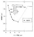
このとき、第1層6aは、幅が広い中央領域R1aのトレンチ5aに形成されたものよりも幅が狭い接続領域R1bのトレンチ5bに形成されたものの方が底部の厚みが大きくなる。これについて、図4および図5を参照して説明する。 At this time, the thickness of the bottom of the
図4は、例えば7μmの深さのトレンチ100の幅Lを変化させて不純物層101の成長量Gの関係を実験により調べた結果を示すグラフである。また、図5は、トレンチ100の幅Lが狭い時(幅L=1μm)と幅Lが広い時(幅L=2.5μm)のときに同じ時間エピタキシャル成長を行ったときのトレンチ100の近傍の断面図である。 FIG. 4 is a graph showing a result of an experiment investigating the relationship between the growth amount G of the
図4に示されるように、幅Lが狭く、例えばアスペクト比が2以上のトレンチ100を不純物層101にて埋め込む場合、マイグレーション効果により幅Lが狭いほど成長レートが大きくなることが実験により判った。そして、図5に示すように、幅Lが狭いものの方が幅Lの広いものよりもトレンチ100の底部における不純物層101の成長量Gが大きくなっていた。また、マイグレーション効果により、トレンチ100の底部において、不純物層101の表面が丸まった形となっていた。 As shown in FIG. 4, when the
したがって、上記したように、中央領域R1aと接続領域R1bそれぞれでトレンチ5a、5bの幅を変えることで、トレンチ5a内に形成される第1層6aの方がトレンチ5bに形成される第1層6aよりも底部の厚くなるようにできる。そして、このような第1層6aの上に第2層6bを形成しているため、第2層6bは、中央領域R1aのトレンチ5a内に形成されたものの方が接続領域R1bのトレンチ5b内に形成されたものよりも深さが深くなる。そして、各第2層6bの底部は、丸まった形状となる。 Therefore, as described above, the
この後、トレンチ5の外部に形成された第1層6aおよび第2層6bの余分な部分を除去するための平坦化工程を行う。これにより、基板表面が平坦になるため、後工程においてフォトリソグラフィ工程をはじめ各種工程を行うときのデバイス加工プロセスが容易に行えるようになる。 Thereafter, a planarization process is performed to remove excess portions of the
〔図3(d)に示す工程〕
p型ベース領域3、n+型ソース領域4およびディープp型層6の上に、図示しないエッチングマスクを成膜したのち、耐圧構造領域R2のトレンチ20の形成予定領域においてエッチングマスクを開口させる。そして、エッチングマスクを用いた異方性エッチングを行ったのち、必要に応じて等方性エッチングや犠牲酸化工程を行うことで、トレンチ20を形成する。この後、エッチングマスクを除去する。[Step shown in FIG. 3 (d)]
After forming an etching mask (not shown) on the p-
次に、p型リサーフ層21の形成予定領域が開口するマスク(図示せず)を配置したのちp型不純物のイオン注入を行う。さらに、p型リサーフ層21の形成の為に用いたマスクを除去した後、n+型コンタクト領域22の形成予定領域が開口するマスク(図示せず)を配置し、n型不純物のイオン注入を行う。そして、活性化のための熱処理などを行うことで、p型リサーフ層21およびn+型コンタクト領域22を形成する。Next, after placing a mask (not shown) in which a region where the p-
また、p型ベース領域3、n+型ソース領域4およびディープp型層6の上に、図示しないエッチングマスクを成膜したのち、セル領域R1のトレンチゲート構造を構成するためのトレンチ7の形成予定領域においてエッチングマスクを開口させる。そして、エッチングマスクを用いた異方性エッチングを行ったのち、必要に応じて等方性エッチングや犠牲酸化工程を行うことで、トレンチ7を形成する。この後、エッチングマスクを除去する。Further, after forming an etching mask (not shown) on the p-
そして、ゲート酸化膜形成工程を行うことでゲート酸化膜8を形成する。具体的には、ウェット雰囲気を用いたパイロジェニック法によるゲート酸化(熱酸化)によりゲート酸化膜8を形成する。 Then, a
続いて、ゲート酸化膜8の表面に例えばn型不純物をドーピングしたポリシリコン層を平坦部の膜厚で約1μm程度、例えば600℃の温度下で成膜し、トレンチ7内を埋込み、エッチバック工程等を行うことにより、トレンチ7内にゲート酸化膜8およびゲート電極9を残す。 Subsequently, a polysilicon layer doped with, for example, an n-type impurity is formed on the surface of the
この後の工程に関しては、従来と同様であるため図示しないが、層間絶縁膜12を成膜したのち、層間絶縁膜12をパターニングしてn+型ソース領域4やディープp型層6に繋がるコンタクトホール、さらにはp型リサーフ層21やn+型コンタクト領域22に繋がるコンタクトホールを形成すると共に、ゲート電極9に繋がるコンタクトホールを別断面に形成する。続いて、コンタクトホール内を埋め込むように電極材料を成膜したのち、これをパターニングすることでソース電極11やゲート配線、外周電極23やEQR電極24を形成する。そして、n+型基板1の裏面にドレイン電極を形成することで、図1に示したMOSFETが完成する。The subsequent steps are the same as in the prior art and are not shown. However, after the
以上説明した製造方法によれば、中央領域R1aと接続領域R1bとで第2層6bの深さが異なる構造となるディープp型層6を同一工程で製造することが可能となる。このため、MOSFETの製造工程の簡略化を図ることが可能となる。そして、同一工程であるため、ドレイン耐圧を異なる構造の中央領域R1aと接続領域R1bを制御性良く形成することが可能となる。 According to the manufacturing method described above, the deep p-
また、第2層6bの下方に形成する第1層6aの表面をマイグレーション効果によって丸めることができるため、第2層6bの底部を丸めることが可能となる。このため、第2層6bの底部が尖っている場合に発生する電界集中による耐圧低下を防止できる構造を形成することが可能となる。 In addition, since the surface of the
また、本実施形態では、第1層6aと第2層6bとを別工程により行っているため、これら第1層6aと第2層6bを別々の不純物濃度に制御できる。このため、第1層6aを第2層6bよりも低濃度となる電界緩和層として機能させることができ、理想的な耐圧構造とすることができる。なお、ここでは電界緩和層として機能させるように、第1層6aをp型SiCにて構成したが、低濃度(例えばn-型ドリフト層2と同程度)のn型SiCにて構成することもできる。このようにしても、第2層6bの底部の深さを中央領域R1aと接続領域R1bとで異ならせることができるし、第2層6bの底部を丸めることができるため、上記効果を得ることができる。In the present embodiment, since the
さらに、第1層6aと第2層6bとを続けて形成しているため、エピタキシャル成長のための昇温や降温にかかる時間を低減できる。しかも第1層6aを形成した後に大気に曝されることがないため、第2層6bを欠陥の少ないものにすることが可能となる。 Furthermore, since the
なお、このようなディープp型層6の形成工程は、1600℃程度の高温で行われることになるが、トレンチ7やゲート酸化膜8さらにはゲート電極9の形成前に完了するため、トレンチゲート構造を保護する必要がない。このため、従来のトレンチゲート構造の形成工程を採用することができる。 The deep p-
(第2実施形態)
本発明の第2実施形態について説明する。本実施形態は、第1実施形態に対してMOSFETの素子構造を変更したものであり、基本構造に関しては第1実施形態と同様であるため、第1実施形態と異なっている部分に関してのみ説明する。(Second Embodiment)
A second embodiment of the present invention will be described. In this embodiment, the element structure of the MOSFET is changed with respect to the first embodiment, and the basic structure is the same as that of the first embodiment. Therefore, only the parts different from the first embodiment will be described. .
図6は、本実施形態にかかるMOSFETの断面図である。この図に示すように、本実施形態では、トレンチゲート構造ではなく、プレーナ型MOSFETに対して本発明の一実施形態を適用している。 FIG. 6 is a cross-sectional view of the MOSFET according to the present embodiment. As shown in this figure, in the present embodiment, one embodiment of the present invention is applied to a planar MOSFET instead of a trench gate structure.
具体的には、本実施形態のMOSFETは、n+型基板1の表面に形成したn-型ドリフト層2の表層部に、複数のp型ベース領域3が互いに所定間隔離間するように配置されてり、その各p型ベース領域3の表層部にn+型ソース領域4が形成された構成とされている。ただし、接続領域R1bに形成されたp型ベース領域3のうち最も外周側に配置されたものにはn+型ソース領域4が備えられていない構造とされている。Specifically, the MOSFET of the present embodiment is arranged on the surface layer portion of the n−
そして、p型ベース領域3のうちn+型ソース領域4およびn-型ドリフト層2の間に位置する部分の表面をチャネル領域として、少なくともチャネル領域の表面にゲート酸化膜8を介してゲート電極9が形成された構造とされている。Then, the surface of the portion of the p-
なお、耐圧構造領域R2は、第1実施形態のようなトレンチ20を形成することなく、n-型ドリフト層2の表層部にp型リサーフ層21およびn+型コンタクト領域22が形成された構造とされている点が第1実施形態と異なっているが、その他は第1実施形態と同様である。The breakdown voltage structure region R2 has a structure in which the p-
このように、プレーナ型のMOSFETに対しても、第1実施形態と同様の構造を採用することができ、第1実施形態と同様の効果を得ることができる。 As described above, the same structure as that of the first embodiment can be adopted for the planar MOSFET, and the same effect as that of the first embodiment can be obtained.
次に、図6に示すプレーナ型のMOSFETの製造方法について説明する。図7は、図6に示すプレーナ型のMOSFETの製造工程を示した断面図である。以下、この図を参照して、図6に示すプレーナ型のMOSFETの製造工程のうち第1実施形態と異なる部分について説明する。 Next, a method for manufacturing the planar type MOSFET shown in FIG. 6 will be described. FIG. 7 is a cross-sectional view showing a manufacturing process of the planar MOSFET shown in FIG. Hereinafter, with reference to this figure, a different part from 1st Embodiment among the manufacturing processes of the planar type MOSFET shown in FIG. 6 is demonstrated.
まず、図7(a)に示す工程において、n+型基板1の表面にn-型ドリフト層2を形成する。First, in the step shown in FIG. 7A, the n−
続いて、図7(b)に示す工程では、まず、p型ベース領域3の形成予定領域が開口するマスク(図示せず)を配置したのちp型不純物のイオン注入を行う。次に、p型ベース領域3の形成の為に用いたマスクを除去した後、n+型ソース領域4の形成予定領域が開口するマスク(図示せず)を配置し、n型不純物のイオン注入を行う。そして、活性化のための熱処理などを行うことで、p型ベース領域3およびn+型ソース領域4を形成する。Subsequently, in the step shown in FIG. 7B, first, a p-type impurity ion implantation is performed after arranging a mask (not shown) in which a region where the p-
さらに、n-型ドリフト層2やp型ベース領域3およびn+型ソース領域4の上に、図示しないエッチングマスクを成膜したのち、トレンチ5の形成予定領域、つまりにp型ベース領域3およびn+型ソース領域4の中央部と対応する位置においてエッチングマスクを開口させる。そして、エッチングマスクを用いた異方性エッチングを行ったのち、必要に応じて等方性エッチングや犠牲酸化工程を行うことで、例えば深さ2.0μm以上とされたトレンチ5を形成する。これにより、中央領域R1aでは、幅が0.8〜1.2μmとされたトレンチ5aが形成され、接続領域R1bでは、幅が0.5〜0.8μmとされたトレンチ5bが形成される。この後、エッチングマスクを除去する。Further, after forming an etching mask (not shown) on the n−
続いて、図7(c)に示す工程において、第1実施形態で説明した図3(c)と同様の工程を行うことにより、トレンチ5内に第1層6aおよび第2層6bからなるディープp型層6を形成する。 Subsequently, in the process shown in FIG. 7C, a deep process composed of the
そして、図7(d)に示す工程において、図3(d)と同様の手法によってp型リサーフ層21およびn+型コンタクト領域22の形成工程を行った後、ゲート酸化によってゲート酸化膜を形成し、さらに、例えばn型不純物をドーピングしたポリシリコン層を成膜してから、これをパターニングすることによりゲート電極9を形成する。この後は、層間絶縁膜12の形成工程やコンタクトホール形成工程、ソース電極11、ゲート配線、外周電極23およびEQR電極24の形成工程、ドレイン電極13の形成工程などを経て、図6に示すプレーナ型のMOSFETが完成する。Then, in the step shown in FIG. 7D, after forming the p-
このような製造方法によってトレンチ5やディープp型層6を形成することにより、第1実施形態に示した製造方法を採用する場合と同様の効果を得ることができる。 By forming the
(第3実施形態)
本発明の第3実施形態について説明する。本実施形態は、SiC半導体装置に備えられる縦型構造の素子として、第1、第2実施形態に示したMOSFETに代えてジャンクションバリアショットキーダイオード(以下、JBSという)を採用したものである。(Third embodiment)
A third embodiment of the present invention will be described. In the present embodiment, a junction barrier Schottky diode (hereinafter referred to as JBS) is employed instead of the MOSFET shown in the first and second embodiments as a vertical structure element provided in the SiC semiconductor device.
図8は、本実施形態にかかるJBSの断面図である。この図に示すように、例えば2×10¹⁸〜1×1021cm-3程度の不純物濃度のSiCからなるn+型基板31の表面に、例えば5×1015cm-3程度不純物濃度とされたn-型ドリフト層32が形成されている。このn-型ドリフト層32の表面に例えばMo(モリブデン)もしくはTi(チタン)等からなるショットキー電極33が形成されていると共に、ショットキー電極33に接続される表面電極34が形成されている。そして、n+型基板31の裏面側に例えばニッケル、チタン、モリブデン、タングステン等により構成されたオーミック接触させられた裏面電極35が形成された構成とされる。FIG. 8 is a cross-sectional view of the JBS according to the present embodiment. As shown in this figure, the impurity concentration is set to about 5 × 1015 cm−3 on the surface of the n+ type substrate 31 made of SiC having an impurity concentration of about 2 × 10¹⁸ to 1 × 1021 cm−3 , for example. An n−
また、耐圧構造領域R2は第2実施形態と同様の構造とされており、第1実施形態のようなトレンチ20を形成することなく、n-型ドリフト層2の表層部にp型リサーフ層21およびn+型コンタクト領域22が形成された構造とされ、これらそれぞれが層間絶縁膜12に形成されたコンタクトホールを通じて外周電極23およびEQR電極24と電気的に接続されている。The breakdown voltage structure region R2 has the same structure as that of the second embodiment, and the p-
そして、このように構成されたJBSにおいても、第1、第2実施形態と同様にディープp型層6を形成している。ディープp型層6は、中央領域R1aにおいて幅広とされ、接続領域R1bにおいて幅狭とされていると共に、中央領域R1aの第1層6aよりも接続領域R1bの第1層6aの方が厚くされている。このため、同じ深さのトレンチ5に形成された第2層6bは、中央領域R1aの方が接続領域R1bよりも深い位置まで形成された構成とされている。 And in JBS comprised in this way, the deep p-
このように、JBSに対しても第1、第2実施形態と同様の構成のディープp型層6を形成することにより、第1、第2実施形態と同様の効果を得ることができる。 As described above, by forming the deep p-
次に、図8に示すJBSの製造方法について説明する。図9は、図8に示すJBSの製造工程を示した断面図である。以下、この図を参照して、図8に示すJBSの製造工程について説明する。 Next, a method for manufacturing the JBS shown in FIG. 8 will be described. FIG. 9 is a cross-sectional view showing a manufacturing process of the JBS shown in FIG. Hereinafter, the manufacturing process of the JBS shown in FIG. 8 will be described with reference to FIG.
まず、図9(a)に示す工程において、n+型基板1の表面にn-型ドリフト層2を形成する。次に、図9(b)に示す工程では、n-型ドリフト層2の上に、図示しないエッチングマスクを成膜したのち、トレンチ5の形成予定領域においてエッチングマスクを開口させる。そして、エッチングマスクを用いた異方性エッチングを行ったのち、必要に応じて等方性エッチングや犠牲酸化工程を行うことで、例えば深さ1.5μm以上とされたトレンチ5を形成する。これにより、中央領域R1aでは、幅が0.7μmとされたトレンチ5aが形成され、接続領域R1bでは、幅が0.4μmとされたトレンチ5bが形成される。この後、エッチングマスクを除去する。First, in the step shown in FIG. 9A, the n−
続いて、図9(c)に示す工程において、第1実施形態で説明した図3(c)と同様の工程を行うことにより、トレンチ5内に第1層6aおよび第2層6bからなるディープp型層6を形成する。 Subsequently, in the process shown in FIG. 9C, a deep process composed of the
そして、図9(d)に示す工程では、p型リサーフ層21およびn+型コンタクト領域22の形成工程、層間絶縁膜12の形成工程やコンタクトホール形成工程、裏面電極35の形成工程、ショットキー電極33の形成工程、表面電極34や外周電極23およびEQR電極24の形成工程などを経て、図8に示すJBSが完成する。9D, the p-
このような製造方法によってトレンチ5やディープp型層6を形成することにより、第1実施形態に示した製造方法を採用する場合と同様の効果を得ることができる。 By forming the
(第4実施形態)
本発明の第4実施形態について説明する。本実施形態は、第1実施形態に対してMOSFETの素子構造を変更したものであり、基本構造に関しては第1実施形態と同様であるため、第1実施形態と異なっている部分に関してのみ説明する。(Fourth embodiment)
A fourth embodiment of the present invention will be described. In this embodiment, the element structure of the MOSFET is changed with respect to the first embodiment, and the basic structure is the same as that of the first embodiment. Therefore, only the parts different from the first embodiment will be described. .
図10は、本実施形態にかかるトレンチゲート型のMOSFETの断面図である。この図に示すように、本実施形態では、トレンチゲート構造を構成するトレンチ7の底部にも更にトレンチ5cを形成し、トレンチ5c内にディープp型層6を形成した構造としている。ただし、このトレンチゲート構造を構成するトレンチ7の下方に形成したトレンチ5cは、中央領域R1aに形成されるものであっても、接続領域R1bに形成されるトレンチ5bと同じ幅とされ、その中に形成される第2層6bよりもトレンチゲート構造の間に位置するトレンチ5a内に形成された第2層6bの方が深くされている。 FIG. 10 is a cross-sectional view of a trench gate type MOSFET according to this embodiment. As shown in this figure, in this embodiment, a
このように、トレンチゲート構造の下方においてディープp型層6を形成することで、オフ時にトレンチ7の角部においてゲート酸化膜8に作用する電界を緩和することが可能となり、ゲート酸化膜8が破壊されることを防止できる。さらに、トレンチゲート構造の間においてp型ベース領域3から延びるように形成されたディープp型層6により、ブレークダウン電流を引抜けるため、L負荷耐量を向上させることができる。 Thus, by forming the deep p-
ただし、トレンチゲート構造の下方に位置するディープp型層6で先にブレークダウンが生じると、ブレークダウン電流がゲート酸化膜8の表面を流れ、ゲート酸化膜8の寿命を低下させることになる。このため、上記したように、トレンチゲート構造の下方に形成されたトレンチ5c内の第2層6bよりもトレンチゲート構造の間に位置するトレンチ5a内に形成された第2層6bの方が深くなるようにすることで、トレンチゲート構造の間に位置するトレンチ5a内に形成されたディープp型層6で優先的にブレークダウンが発生するようにしている。これにより、ブレークダウン電流がゲート酸化膜8の表面に流れることを防止でき、ゲート酸化膜8の寿命を低下させることなくブレークダウン電流の引抜を行うことが可能となる。 However, if breakdown occurs first in the deep p-
次に、図10に示すトレンチゲート構造のMOSFETの製造方法について説明する。図11は、図10に示すトレンチゲート構造のMOSFETの製造工程を示した断面図である。以下、この図を参照して説明するが、本実施形態のトレンチゲート構造のMOSFETの製造工程は、第1実施形態とほぼ同様であるため、異なる部分についてのみ説明する。 Next, a method for manufacturing the MOSFET having the trench gate structure shown in FIG. 10 will be described. 11 is a cross-sectional view showing a manufacturing process of the MOSFET having the trench gate structure shown in FIG. Hereinafter, the manufacturing process of the MOSFET having the trench gate structure according to the present embodiment is substantially the same as that of the first embodiment, and therefore only different portions will be described.
まず、図11(a)に示す工程では、図3(a)と同様の工程を行う。続いて、図11(b)に示す工程において、図3(b)と同様にトレンチ5の工程を行うが、このときに中央領域R1aおよび接続領域R1bにおけるトレンチゲート構造の間に形成されるトレンチ5a、5bに加えて、トレンチゲート構造の下方に位置するトレンチ5cも同時に形成する。そして、図11(c)に示す工程において、図3(c)と同様の工程を行う。これにより、トレンチゲート構造の下方に位置するトレンチ5c内にも第1層6aおよび第2層6bが配置される。このトレンチ5c内に配置された第1層6aの厚みや第2層6bの深さは、接続領域R1bのトレンチ5b内に配置された第1層6aの厚みや第2層6bの深さと同じになる。この後、図11(d)に示す工程において、図3(d)と同様の工程を行うことにより、図10に示したトレンチゲート構造のMOSFETが完成する。 First, in the process shown in FIG. 11A, the same process as in FIG. Subsequently, in the step shown in FIG. 11B, the step of the
このように、トレンチ5a、5bと同時にトレンチ5cを形成すると共に、トレンチ5a、5b内にディープp型層6を形成する際に同時にトレンチ5c内のディープp型層6も形成するようにしているため、製造工程の簡略化を図ることが可能となる。 In this way, the
(他の実施形態)
上記各実施形態では、第1導電型をn型とし、第2導電型をp型とするSiC半導体装置について説明したが、各導電型を反転させた構造としても良い。(Other embodiments)
In each of the embodiments described above, the SiC semiconductor device in which the first conductivity type is n-type and the second conductivity type is p-type has been described, but a structure in which each conductivity type is inverted may be used.
また、上記第1、第2実施形態では縦型構造のMOSFET、第3実施形態では、縦型構造のJBSを例に挙げて説明したが、その他の縦型構造の素子、例えばIGBT、PNダイオードなど、ディープ層を形成できるような素子に対して本発明を適用することができる。 In the first and second embodiments, the vertical structure MOSFET has been described as an example, and in the third embodiment, the vertical structure JBS has been described as an example. However, other vertical structure elements such as IGBTs and PN diodes have been described. The present invention can be applied to an element that can form a deep layer.
さらに、各実施形態ではディープp型層6を形成するための領域を2つに分け、トレンチ幅も2種類として説明したが、本発明は、セル中央領域で面状にブレークダウンを発生させるように設計すれば良く、トレンチ幅も連続的に変化させ、第2層6bの深さも連続的に変化させても同様な効果が得られる。 Further, in each of the embodiments, the region for forming the deep p-
1 n+型基板
2 n-型ドリフト層
3 p型ベース領域
4 n+型ソース領域
5 トレンチ
6 ディープp型層
6a 第1層
6b 第2層
7 トレンチ
8 ゲート酸化膜
9 ゲート電極
11 ソース電極
13 ドレイン電極
31 n+型基板
32 n-型ドリフト層
33 ショットキー電極
34 表面電極
35 裏面電極
R1 セル領域
R1a 中央領域
R1b 接続領域
R2 耐圧構造領域1 n+ type substrate 2 n− type drift layer 3 p type base region 4 n+
Claims (11)
Translated fromJapanese前記基板(1、31)の表面に形成された炭化珪素からなる第1導電型のドリフト層(2、32)と、を有し、
前記基板(1、31)内のセル領域(R1)において前記基板(1、31)の表面側に形成された表面電極(11、34)と裏面側に形成された裏面電極(13、35)との間で電流を流す縦型構造の半導体素子が形成されていると共に、前記セル領域(R1)の外周を囲むように耐圧構造領域(R2)が形成されてなる炭化珪素半導体装置において、
前記セル領域(R1)における中央領域(R1a)と、該中央領域(R1a)を囲むように構成されていると共に、前記中央領域(R1a)と前記耐圧構造領域(R2)の間を接続するように配置された接続領域(R1b)の双方に、前記表面電極(11、34)との接触表面から前記ドリフト層(2、32)に達する第2導電型のディープ層(6)が備えられ、該ディープ層(6)により前記中央領域(R1a)の耐圧(BV(R1a))の方が前記接続領域(R1b)における耐圧(BV(R1b))よりも低く、かつ、前記接続領域(R1b)における耐圧(BV(R1b))の方が前記耐圧構造領域(R2)における耐圧(BV(R2))よりも低くされており、
前記セル領域(R1)における中央領域(R1a)と前記接続領域(R1b)の双方に、前記ドリフト層(2、32)に達するトレンチ(5)が形成されていると共に該トレンチ(5)内に第2導電型層(6b)を有するディープ層(6)が備えられ、
前記中央領域(R1a)に形成された前記第2導電型層(6b)の方が前記接続領域(R1b)に形成された前記第2導電型層(6b)よりも深くされていることを特徴とする炭化珪素半導体装置。A first conductivity type or second conductivity type substrate (1, 31) made of silicon carbide;
A drift layer (2, 32) of the first conductivity type made of silicon carbide formed on the surface of the substrate (1, 31),
In the cell region (R1) in the substrate (1, 31), the surface electrode (11, 34) formed on the front surface side of the substrate (1, 31) and the back electrode (13, 35) formed on the back surface side. In a silicon carbide semiconductor device in which a vertical structure semiconductor element is formed to pass a current between and a breakdown voltage structure region (R2) is formed so as to surround an outer periphery of the cell region (R1).
The central region (R1a) in the cell region (R1) is configured to surround the central region (R1a), and the central region (R1a) and the breakdown voltage structure region (R2) are connected to each other. A deep layer (6) of the second conductivity type that reaches the drift layer (2, 32)from the contact surface with the surface electrode (11, 34) in both of the connection regions (R1b) disposed in Due to the deep layer (6), the breakdown voltage (BV (R1a)) of the central region (R1a) is lower than the breakdown voltage (BV (R1b)) of the connection region (R1b), and the connection region (R1b) The withstand voltage (BV (R1b)) at is lower than the withstand voltage (BV (R2)) in the withstand voltage structure region (R2),
A trench (5) reaching the drift layer (2, 32) is formed in both the central region (R1a) and the connection region (R1b) in the cell region (R1), and in the trench (5). A deep layer (6) having a second conductivity type layer (6b) is provided;
The second conductivity type layer (6b) formed in the central region (R1a) is deeper than the second conductivity type layer (6b) formed in the connection region (R1b). A silicon carbide semiconductor device.
前記第1層(6a)は、前記トレンチ(5)の底部からの厚みが、前記中央領域(R1a)に形成された前記第1層(6a)よりも前記接続領域(R1b)に形成された前記第1層(6a)の方が厚くなっていることを特徴とする請求項1に記載の炭化珪素半導体装置。A first layer (6a) formed at the bottom of the trench (5) and having a second conductivity type or a first conductivity type having a lower concentration than the second conductivity type layer (6b); And the second conductivity type layer (6b) is a second layer (6b) formed on the first layer (6a),
The thickness of the first layer (6a) from the bottom of the trench (5) is formed in the connection region (R1b) rather than the first layer (6a) formed in the central region (R1a). The silicon carbide semiconductor device according to claim1 , wherein the first layer (6a) is thicker.
前記トレンチゲート構造を構成するための前記トレンチ(7)の下方にも、前記ディープ層(6)が形成されていることを特徴とする請求項1ないし4のいずれか1つに記載の炭化珪素半導体装置。The vertical semiconductor device includes a second conductivity type base region (3) formed on the drift layer (2) and a first conductivity type formed on the base region (3). A source region (4), a trench (7) reaching the drift layer (2) through the source region (4) and the base region (3), and a gate formed on the inner wall of the trench (7) An insulating film (8), a gate electrode (9) formed on the surface of the gate oxide film (8), a source electrode (4) electrically connected to the source region (4) and the base region (3) 11) and a back surface electrode (13) formed on the back surface of the substrate (1), a trench gate structure element,
The silicon carbide according to anyone of claims1 to4 , wherein the deep layer (6) is also formed below the trench (7) for forming the trench gate structure. Semiconductor device.
前記基板(1、31)の上に前記ドリフト層(2、32)を形成する工程と、
前記セル領域(R1)における中央領域(R1a)および前記中央領域(R1a)を囲み該中央領域(R1a)と前記耐圧構造領域(R2)の間を接続するように配置された接続領域(R1b)の双方に、前記セル領域(R1)に前記ドリフト層(2、32)の所定深さまで達するトレンチ(5)を形成し、かつ、前記中央領域(R1a)に形成される前記トレンチ(5a)の方が前記接続領域(R1b)に形成される前記トレンチ(5b)よりも幅が広くなるように形成する工程と、
前記中央領域(R1a)および前記接続領域(R1b)の前記トレンチ(5a、5b)内に、前記第2導電型層(6b)よりも低濃度とされた第2導電型または第1導電型にて構成された第1層(6a)をエピタキシャル成長させると共に、該第1層(6a)の上に第2導電型の第2層(6b)をエピタキシャル成長させることにより、前記第1層(6a)および前記第2層(6b)を含むディープ層(6)を形成する工程と、を含んでいることを特徴とする炭化珪素半導体装置の製造方法。After preparing a first conductivity type or second conductivity type substrate (1, 31) made of silicon carbide and forming a first conductivity type drift layer (2, 32) on the surface of the substrate (1, 31). In the cell region (R1) in the substrate (1, 31), the surface electrode (11, 34) formed on the surface side of the substrate (1, 31) and the back electrode (13, 35) formed on the back surface side. In the method for manufacturing a silicon carbide semiconductor device, the semiconductor device having a vertical structure in which a current flows between the semiconductor region and the cell region (R1) and the breakdown voltage region (R2) is formed so as to surround the outer periphery of the cell region (R1).
Forming the drift layer (2, 32) on the substrate (1, 31);
A central region (R1a) in the cell region (R1) and a connection region (R1b) disposed so as to surround the central region (R1a) and connect the central region (R1a) and the breakdown voltage structure region (R2). The trench (5) reaching the predetermined depth of the drift layer (2, 32) is formed in the cell region (R1), and the trench (5a) formed in the central region (R1a) Forming a width wider than the trench (5b) formed in the connection region (R1b);
In the trenches (5a, 5b) in the central region (R1a) and the connection region (R1b), the second conductivity type or the first conductivity type having a lower concentration than the second conductivity type layer (6b). The first layer (6a) configured as described above is epitaxially grown and the second layer (6b) of the second conductivity type is epitaxially grown on the first layer (6a). Forming a deep layer (6) including the second layer (6b). A method for manufacturing a silicon carbide semiconductor device, comprising:
前記ディープ層(6)を形成する工程では、前記第1層(6a)および前記第2層(6b)を1600℃以上の成長温度にてエピタキシャル成長させることを特徴とする請求項8または9に記載の炭化珪素半導体装置の製造方法。In the step of forming the trench (5), the trench (5) is formed with an aspect ratio of 2 or more,
In the step of forming the deep layer (6), according to claim8 or9, characterized in that epitaxial growth in the first layer (6a) and said second layer (6b) to 1600 ° C. or more growth temperature A method for manufacturing a silicon carbide semiconductor device.
前記トレンチゲート構造を構成するための前記トレンチ(7)の下方にも、前記ディープ層(6)を形成する工程を有し、
前記トレンチゲート構造を形成する前に、前記トレンチ(7)の下方に前記ディープ層(6)を形成する工程と、前記中央領域(R1a)および前記接続領域(R1b)の前記トレンチ(5a、5b)内に前記第1層(6a)および前記第2層(6b)を形成することで前記ディープ層(6)を形成する工程とを同時に行うことを特徴とする請求項8ないし10のいずれか1つに記載の炭化珪素半導体装置の製造方法。The vertical semiconductor device includes a second conductivity type base region (3) formed on the drift layer (2) and a first conductivity type formed on the base region (3). A source region (4), a trench (7) that penetrates the source region (4) and the base region (3) and reaches the drift layer (2, 32), and an inner wall of the trench (7) are formed. The gate insulating film (8), the gate electrode (9) formed on the surface of the gate oxide film (8), and the source electrically connected to the source region (4) and the base region (3) An element having a trench gate structure having an electrode (11) and a back electrode (13) formed on the back surface of the substrate (1);
Forming the deep layer (6) also below the trench (7) for forming the trench gate structure;
Before forming the trench gate structure, forming the deep layer (6) below the trench (7), and the trenches (5a, 5b) in the central region (R1a) and the connection region (R1b). ) one of the first layer (6a) and said second layer (the preceding claims8 and performs the deep layer by forming a 6b) and forming a (6) at the same time10 in The manufacturing method of the silicon carbide semiconductor device as described in one.
Priority Applications (2)
| Application Number | Priority Date | Filing Date | Title |
|---|---|---|---|
| JP2008151370AJP4683075B2 (en) | 2008-06-10 | 2008-06-10 | Silicon carbide semiconductor device and manufacturing method thereof |
| SE0900780ASE533962C2 (en) | 2008-06-10 | 2009-06-09 | Semiconductor device of silicon carbide and process for making such |
Applications Claiming Priority (1)
| Application Number | Priority Date | Filing Date | Title |
|---|---|---|---|
| JP2008151370AJP4683075B2 (en) | 2008-06-10 | 2008-06-10 | Silicon carbide semiconductor device and manufacturing method thereof |
Publications (2)
| Publication Number | Publication Date |
|---|---|
| JP2009302091A JP2009302091A (en) | 2009-12-24 |
| JP4683075B2true JP4683075B2 (en) | 2011-05-11 |
Family
ID=41503561
Family Applications (1)
| Application Number | Title | Priority Date | Filing Date |
|---|---|---|---|
| JP2008151370AExpired - Fee RelatedJP4683075B2 (en) | 2008-06-10 | 2008-06-10 | Silicon carbide semiconductor device and manufacturing method thereof |
Country Status (2)
| Country | Link |
|---|---|
| JP (1) | JP4683075B2 (en) |
| SE (1) | SE533962C2 (en) |
Families Citing this family (18)
| Publication number | Priority date | Publication date | Assignee | Title |
|---|---|---|---|---|
| KR101481878B1 (en)* | 2010-04-06 | 2015-01-12 | 미쓰비시덴키 가부시키가이샤 | Power semiconductor device, power module and method for manufacturing power semiconductor device |
| JP5621340B2 (en)* | 2010-06-16 | 2014-11-12 | 株式会社デンソー | Silicon carbide semiconductor device manufacturing method and silicon carbide semiconductor device |
| WO2012001837A1 (en)* | 2010-06-30 | 2012-01-05 | 三菱電機株式会社 | Power semiconductor device |
| US9318623B2 (en)* | 2011-04-05 | 2016-04-19 | Cree, Inc. | Recessed termination structures and methods of fabricating electronic devices including recessed termination structures |
| JP5482745B2 (en) | 2011-08-10 | 2014-05-07 | 株式会社デンソー | Silicon carbide semiconductor device and manufacturing method thereof |
| CN102263128B (en)* | 2011-08-12 | 2014-04-09 | 淄博美林电子有限公司 | High voltage-resistant IGBT |
| JP5812029B2 (en)* | 2012-06-13 | 2015-11-11 | 株式会社デンソー | Silicon carbide semiconductor device and manufacturing method thereof |
| CN104241341A (en)* | 2012-07-27 | 2014-12-24 | 俞国庆 | High-frequency low-power dissipation power MOS field-effect tube device |
| JP6164636B2 (en)* | 2013-03-05 | 2017-07-19 | ローム株式会社 | Semiconductor device |
| JP6164604B2 (en)* | 2013-03-05 | 2017-07-19 | ローム株式会社 | Semiconductor device |
| KR102145909B1 (en)* | 2013-12-19 | 2020-08-19 | 엘지이노텍 주식회사 | Power Semiconductor Device and Power semiconductor circuit including the device |
| JP6354525B2 (en)* | 2014-11-06 | 2018-07-11 | 株式会社デンソー | Method for manufacturing silicon carbide semiconductor device |
| DE102015215024B4 (en)* | 2015-08-06 | 2019-02-21 | Infineon Technologies Ag | Wide bandgap semiconductor device and method of operating a semiconductor device |
| JP6651894B2 (en)* | 2016-02-23 | 2020-02-19 | 株式会社デンソー | Compound semiconductor device and method of manufacturing the same |
| JP6485383B2 (en)* | 2016-02-23 | 2019-03-20 | 株式会社デンソー | Compound semiconductor device and method of manufacturing the same |
| DE102017127848B4 (en) | 2017-11-24 | 2024-10-17 | Infineon Technologies Ag | silicon carbide semiconductor device with edge termination structure |
| CN113031752A (en)* | 2021-03-23 | 2021-06-25 | 维沃移动通信有限公司 | Chip voltage adjusting method, performance testing method and device and electronic equipment |
| US12402390B2 (en) | 2022-07-13 | 2025-08-26 | Leap Semiconductor Corp. | Method of manufacturing silicon carbide semiconductor power device |
Family Cites Families (5)
| Publication number | Priority date | Publication date | Assignee | Title |
|---|---|---|---|---|
| JP2701502B2 (en)* | 1990-01-25 | 1998-01-21 | 日産自動車株式会社 | Semiconductor device |
| JP3785794B2 (en)* | 1998-03-18 | 2006-06-14 | 株式会社デンソー | Silicon carbide semiconductor device and manufacturing method thereof |
| JP3921816B2 (en)* | 1998-06-12 | 2007-05-30 | 株式会社デンソー | Silicon carbide semiconductor device and manufacturing method thereof |
| JP4568929B2 (en)* | 1999-09-21 | 2010-10-27 | 株式会社デンソー | Silicon carbide semiconductor device and manufacturing method thereof |
| JP4736180B2 (en)* | 2000-11-29 | 2011-07-27 | 株式会社デンソー | Semiconductor device and manufacturing method thereof |
- 2008
- 2008-06-10JPJP2008151370Apatent/JP4683075B2/ennot_activeExpired - Fee Related
- 2009
- 2009-06-09SESE0900780Apatent/SE533962C2/ennot_activeIP Right Cessation
Also Published As
| Publication number | Publication date |
|---|---|
| JP2009302091A (en) | 2009-12-24 |
| SE533962C2 (en) | 2011-03-15 |
| SE0900780L (en) | 2009-12-11 |
Similar Documents
| Publication | Publication Date | Title |
|---|---|---|
| JP4683075B2 (en) | Silicon carbide semiconductor device and manufacturing method thereof | |
| JP4798119B2 (en) | Silicon carbide semiconductor device and manufacturing method thereof | |
| JP5812029B2 (en) | Silicon carbide semiconductor device and manufacturing method thereof | |
| JP6048317B2 (en) | Silicon carbide semiconductor device | |
| JP5326405B2 (en) | Wide band gap semiconductor device | |
| CN110050349B (en) | Silicon carbide semiconductor device and method of manufacturing the same | |
| JP5710644B2 (en) | Silicon carbide semiconductor device and manufacturing method thereof | |
| JP5728992B2 (en) | Silicon carbide semiconductor device and manufacturing method thereof | |
| JP4899405B2 (en) | Silicon carbide semiconductor device and manufacturing method thereof | |
| US9825164B2 (en) | Silicon carbide semiconductor device and manufacturing method for same | |
| JP6740759B2 (en) | Silicon carbide semiconductor device and manufacturing method thereof | |
| JP6485382B2 (en) | Method of manufacturing compound semiconductor device and compound semiconductor device | |
| JP2009094203A (en) | Silicon carbide semiconductor device | |
| JP6696329B2 (en) | Silicon carbide semiconductor device and manufacturing method thereof | |
| JP6696328B2 (en) | Silicon carbide semiconductor device and manufacturing method thereof | |
| JP7643621B2 (en) | Semiconductor Device | |
| JP2015072999A (en) | Silicon carbide semiconductor device | |
| JP2010147222A (en) | Silicon carbide semiconductor device and method of manufacturing the same | |
| JP7420485B2 (en) | Silicon carbide semiconductor device and its manufacturing method | |
| TWI633674B (en) | Semiconductor device and manufacturing method of semiconductor device | |
| JP2017152489A (en) | Compound semiconductor device and manufacturing method for the same | |
| WO2017187856A1 (en) | Semiconductor device | |
| JP4755439B2 (en) | Semiconductor device and manufacturing method thereof | |
| JP2012182405A (en) | Semiconductor rectifier | |
| JP6092680B2 (en) | Semiconductor device and manufacturing method of semiconductor device |
Legal Events
| Date | Code | Title | Description |
|---|---|---|---|
| A621 | Written request for application examination | Free format text:JAPANESE INTERMEDIATE CODE: A621 Effective date:20091118 | |
| A977 | Report on retrieval | Free format text:JAPANESE INTERMEDIATE CODE: A971007 Effective date:20100811 | |
| A131 | Notification of reasons for refusal | Free format text:JAPANESE INTERMEDIATE CODE: A131 Effective date:20100817 | |
| A521 | Request for written amendment filed | Free format text:JAPANESE INTERMEDIATE CODE: A523 Effective date:20101012 | |
| TRDD | Decision of grant or rejection written | ||
| A01 | Written decision to grant a patent or to grant a registration (utility model) | Free format text:JAPANESE INTERMEDIATE CODE: A01 Effective date:20110111 | |
| A01 | Written decision to grant a patent or to grant a registration (utility model) | Free format text:JAPANESE INTERMEDIATE CODE: A01 | |
| A61 | First payment of annual fees (during grant procedure) | Free format text:JAPANESE INTERMEDIATE CODE: A61 Effective date:20110124 | |
| FPAY | Renewal fee payment (event date is renewal date of database) | Free format text:PAYMENT UNTIL: 20140218 Year of fee payment:3 | |
| R151 | Written notification of patent or utility model registration | Ref document number:4683075 Country of ref document:JP Free format text:JAPANESE INTERMEDIATE CODE: R151 | |
| FPAY | Renewal fee payment (event date is renewal date of database) | Free format text:PAYMENT UNTIL: 20140218 Year of fee payment:3 | |
| R250 | Receipt of annual fees | Free format text:JAPANESE INTERMEDIATE CODE: R250 | |
| R250 | Receipt of annual fees | Free format text:JAPANESE INTERMEDIATE CODE: R250 | |
| R250 | Receipt of annual fees | Free format text:JAPANESE INTERMEDIATE CODE: R250 | |
| R250 | Receipt of annual fees | Free format text:JAPANESE INTERMEDIATE CODE: R250 | |
| R250 | Receipt of annual fees | Free format text:JAPANESE INTERMEDIATE CODE: R250 | |
| R250 | Receipt of annual fees | Free format text:JAPANESE INTERMEDIATE CODE: R250 | |
| R250 | Receipt of annual fees | Free format text:JAPANESE INTERMEDIATE CODE: R250 | |
| R250 | Receipt of annual fees | Free format text:JAPANESE INTERMEDIATE CODE: R250 | |
| R250 | Receipt of annual fees | Free format text:JAPANESE INTERMEDIATE CODE: R250 | |
| LAPS | Cancellation because of no payment of annual fees |