JP4678277B2 - Non-contact IC card reader device - Google Patents
Non-contact IC card reader deviceDownload PDFInfo
- Publication number
- JP4678277B2 JP4678277B2JP2005310895AJP2005310895AJP4678277B2JP 4678277 B2JP4678277 B2JP 4678277B2JP 2005310895 AJP2005310895 AJP 2005310895AJP 2005310895 AJP2005310895 AJP 2005310895AJP 4678277 B2JP4678277 B2JP 4678277B2
- Authority
- JP
- Japan
- Prior art keywords
- contact
- card
- card reader
- base
- housing
- Prior art date
- Legal status (The legal status is an assumption and is not a legal conclusion. Google has not performed a legal analysis and makes no representation as to the accuracy of the status listed.)
- Expired - Fee Related
Links
Images


Landscapes
- Details Of Aerials (AREA)
- Near-Field Transmission Systems (AREA)
Description
Translated fromJapanese本発明は、ICカードとの間において、非接触で通信を行うICカードリーダ装置に関し、例えば入退室管理システム、自動改札システム、電子マネー等におけるIDカード、管理カード、定期券、回数券、キャッシュカード等の非接触式ICカードとの間において、非接触で通信を行う非接触ICカードリーダ装置に関するものである。 The present invention relates to an IC card reader device that performs contactless communication with an IC card. For example, an ID card, a management card, a commuter pass, a coupon ticket, a cash in an entry / exit management system, an automatic ticket gate system, electronic money, etc. The present invention relates to a non-contact IC card reader device that performs non-contact communication with a non-contact IC card such as a card.
従来より、壁面に埋め込んで取り付ける非接触ICカードリーダ装置では、ICカードと通信を行うループアンテナと、送受信データの変復調を行うと共に、カードリーダを制御する制御部と、これらを格納する筐体を有するものがある。そして、筐体を壁面に埋め込んで取り付けるために、取付け枠,前面を保護する化粧パネル、化粧パネルを取り付けるベースを備えている。 Conventionally, in a non-contact IC card reader device that is embedded in a wall surface, a loop antenna that communicates with an IC card, modulation / demodulation of transmission / reception data, a control unit that controls the card reader, and a housing that stores these There is something to have. And in order to embed a housing | casing in a wall surface, the attachment frame, the decorative panel which protects a front surface, and the base which attaches a decorative panel are provided.
上記のような非接触ICカードリーダ装置においては、ICカードと通信を行うためのループアンテナは筐体内に設けている。しかも、取付け枠やベースや化粧パネルのサイズに対して相対的に筐体のサイズを小さくしなければならない。従って、筐体内に格納するループアンテナのサイズが小さくなってしまった。 In the non-contact IC card reader as described above, a loop antenna for communicating with the IC card is provided in the housing. In addition, the size of the housing must be made relatively small with respect to the size of the mounting frame, base, and decorative panel. Therefore, the size of the loop antenna stored in the housing has been reduced.
ループアンテナのサイズはICカードの読取り可能距離を決める重要な要素であり、ループアンテナのサイズが小さくなることにより、ICカードの読取り可能距離が短くなってしまうという問題点がある。 The size of the loop antenna is an important factor that determines the readable distance of the IC card, and there is a problem in that the readable distance of the IC card is shortened by reducing the size of the loop antenna.
また、取付け枠が金属等の導体の場合にはループアンテナから発生する交流磁界により、渦電流が発生してアンテナ特性を劣化させ、ICカードの読取り距離が短くなってしまうという問題点もある。 Further, when the mounting frame is a conductor such as metal, there is a problem in that an eddy current is generated due to an alternating magnetic field generated from the loop antenna, the antenna characteristics are deteriorated, and the reading distance of the IC card is shortened.
また、美観上の観点からループアンテナを含む筐体は壁面からの突出をさけるために、取付け枠よりも後方に配置されることも、ICカードの読取り距離が短くなってしまう原因となっている。 In addition, from the aesthetic point of view, the housing including the loop antenna is disposed behind the mounting frame in order to avoid protrusion from the wall surface, which causes a reduction in the reading distance of the IC card. .
非接触ICカードリーダ装置のアンテナの取り付け方法について、アンテナの位置関係が大きくずれることなく、安定的に維持するようにした技術として、例えば、特許文献1が提案されている。 For example,
特許文献1の非接触ICカードリーダ装置は、送信アンテナから電磁波を送信し非接触ICカードから送信された電磁波を受信アンテナで受信する。これらのアンテナのうち少なくとも一方はコイルとし、コイルを保持する絶縁性を有する基板と、コイルを基板に固定する取付け手段を有している。取付け手段は基板の所定位置にコイルを固定するためのものであり、それぞれコイルを横切って、基板のコイル配置位置に配設された透孔に係合し、コイルを所定位置に固定する。 The non-contact IC card reader device of
また、壁面埋め込み式の非接触ICカードリーダ装置のアンテナについて、アンテナの操作面側表面近傍の金属体がアンテナの通信可能な距離に影響を与えないようにした非接触ICカードリーダ装置が知られている(例えば、特許文献2)。この特許文献2には、アンテナの操作面側表面近傍の金属性化粧部材により読みとり距離に影響を与えないように、化粧部材に切り込みを付けた技術が開示されている。
上記特許文献1の非接触ICカードリーダ装置によれば、アンテナを効率よく固定できるようにしたことについて開示されている。しかし、特許文献1には、壁面に埋め込む非接触ICカードリーダにおいて、アンテナをできるだけ前面に出すことによって壁面からICカードまでの通信可能距離をできるだけ延ばせるようにすることや、通信感度および通信可能距離をかせぐためにアンテナを大きくすることについては記載されていない。 According to the non-contact IC card reader device of
また、特許文献2は、アンテナの操作面側表面近傍の金属性化粧部材によってICカードを読み取り可能な距離(通信可能距離)に影響を与えないようにした非接触ICカードリーダに関するもので、化粧部材に切り込みを付けた技術が開示されている。しかし、壁面からICカードまでの通信可能距離をできるだけ延ばせるようにすることや、通信感度および通信可能距離をかせぐためにアンテナを大きくすることについては記載されていない。
本発明は、上記のような問題点に鑑みてなされたものであって、ICカードまでの通信可能距離をできるだけ延ばせるようにすべく、アンテナのサイズを大きくとれてアンテナ特性の劣化を防げる非接触ICカードリーダ装置を提供することを目的とする。 The present invention has been made in view of the above-described problems, and is a non-contact type that can prevent the deterioration of antenna characteristics by increasing the size of the antenna so as to extend the communicable distance to the IC card as much as possible. An object is to provide an IC card reader device.
本発明の請求項1に係る非接触ICカードリーダ装置は、上述のような目的を達成するために、カードリーダ全体の動作を制御する本体制御部および送受信データの変復調を行う無線回路部とを格納する筐体と、非接触ICカード又はアクティブタグとの通信を行うための交流磁界を発生するループアンテナと、枠体の中央部に設けられた開口周縁に前記筐体を係止保持する係止部材が形成された取付け枠と、この取付け枠と嵌合する面とは反対側の面である前面に化粧パネルが取り付けられて前記取付け枠と前記化粧パネルとを一体化する金属性のベースと、このベースと前記取付け枠と前記筐体とを覆って前記ベースに取り付けられる化粧パネルとを有し、非接触ICカード又はアクティブタグと非接触に通信を行う非接触ICカードリーダ装置であって、
取り付け先である壁面に向かう正対視で、前記ループアンテナが、前記ベースの前面に、絶縁性の磁性体層を介して、前記筐体よりも大きく巻回されて積層されてなることを特徴とする。
Noncontact IC card reader according to
The loop antenna is wound to be larger than the casing and laminated on the front surface of the base through an insulating magnetic layer in a front-facing view toward the wall surface as an attachment destination. And
本発明の請求項1に係る非接触ICカードリーダ装置によれば、筐体のサイズにとらわれずにアンテナのサイズ、すなわち正面寸法(有効送受信面積)を大きく設計できるとともに、前面すなわち、筐体より壁面寄り、つまりICカード寄り)に配置されるベースに積層して一体化して構成するので、アンテナ特性の劣化を小さくでき、通信可能距離など通信性能を向上させることができる。ここで、絶縁材である磁性体層を用いて周囲金属であるベースとループアンテナとのあいだの絶縁を可能としたので、周囲金属であるベースによる電磁気的な余計な影響を防ぎ、性能の向上を図ることができる。しかも、ベースを金属製としたので構造上の強度を確保できる。 According to the non-contact IC card reader device according to
次に、本発明の最良の形態を図面に基づいて詳細に説明する。 Next, the best mode of the present invention will be described in detail with reference to the drawings.
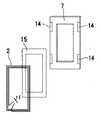
図1は、本発明に係る非接触ICカードリーダ装置の一実施例を示す分解斜視図、図2はそれを壁面に取り付けた状態の断面側面図、図3はその筐体の構成を示す断面図、図4はそのアンテナ一体化ベースの分解斜視図である。 FIG. 1 is an exploded perspective view showing an embodiment of a non-contact IC card reader device according to the present invention, FIG. 2 is a cross-sectional side view in a state where it is attached to a wall surface, and FIG. 4 and 4 are exploded perspective views of the antenna integrated base.
図に示すように、本実施例の非接触ICカードリーダ装置(以下、単にICカードリーダ装置ともいう)1は、ICカード(図示していない)への給電および通信を行うためのループアンテナ2と、カードリーダ全体の動作を制御する本体制御部3(図3参照)と、送受信データの変復調を行う無線回路部4(図3参照)と、本体制御部3および無線回路部4を格納する筐体5とを有する。さらに、図1、2に示すように筐体5を壁面に取り付けるための取付け枠6、化粧板(以下では化粧パネルとも称する)8と、化粧パネル8を壁9に取り付けるためのベース7を有している。 As shown in the figure, a non-contact IC card reader device (hereinafter also simply referred to as an IC card reader device) 1 of the present embodiment includes a
ループアンテナ2は誘電体の基板に印刷又はエッチングにより導体パターンが形成され又は導体が巻かれて形成され、ICカードに給電および/または通信を行うために印加される交流電流の瞬間的な変化量に応じて交流磁界を発生する働きをするものである。そして、ループアンテナ2は金属製の正面ロ字状の中空板状材からなるベース7に磁性体層15を介して積層されて接着され、ICカードリーダ側のベース7と一体的に形成されている。そして、ループアンテナ2の端部に、リード線11が接続されて裏面側に導出されている。リード線11は筐体5の中の本体制御部3に接続し、ループアンテナ2で受けた磁気信号を、ループアンテナ2を挿通する磁束変化量を基にして電磁誘導の法則に従って生じた電流として本体制御部3へ伝え、逆に本体制御部3を起点として生成された信号電流をループアンテナ2に流す。 The
本体制御部3はカードリーダ全体の動作を制御する部分であり、基板に設けられて筐体5内に格納されており、無線回路部4で復調された信号を受けてカードリーダ全体の動作をしたり、無線回路部4に変調信号を生成させたりする。無線回路部4はループアンテナ2で送受信するデータの変復調を行うものであり、これも本体制御部3と同様に基板に設けられて筐体5内に格納されており、本体制御部3にコントロールされて通信動作するものである。 The main
筐体5は取付け枠6の係止部材12に係止可能な爪構造(不図示)が表面に形成されたほぼ箱形をなし、基板に設けられた本体制御部3および無線回路部4を内部に格納し、その外面の爪構造(不図示)を取付け枠6の係止部材12に係止されることで取付け枠6に固定されて、その大部分は壁面の中に入り込んで設置される。 The
取付け枠6はプラスチックで形成され、中央部が開口し、この開口に面して筐体5を係止保持する係止部材12を形成されてある。また、取付け枠6の対向する1対の辺には壁9に取り付けるべく一対の挿通穴10、10が設けられている。そして、この挿通穴10にねじ13、13を挿通し、壁9に取付け枠6を固定する。これにより、開口に嵌合した筐体5を壁9に取り付ける。 The
ベース7は薄板ではあるが薄板でも構造上強度を損なわないように金属製のものとして形成されており、電気的絶縁性材質である磁性体層15を介して(図4参照)ループアンテナ2と一体化され、取付け枠6と係合して不用意に外れないようにする係止部(不図示)を有するとともに、前面側に化粧パネル8を装着可能とするように化粧パネル8を固定する係合部14が形成されている。 Although the
上記のように構成したICカードリーダ装置1は、筐体5が取付け枠6に嵌合して係止保持され、取付け枠6を壁9面にねじ13により固定して、更に取付け枠6に、前面側から(つまり壁裏面からではなく壁前面側である室内側から)ループアンテナ2と一体化したベース7及び化粧パネル8を、取り付ける。 In the IC
ICカードをICカードリーダ装置1の化粧パネル8面にかざすと、ICカードリーダ装置1から発する交流磁界により、ICカードのアンテナに電流が流れて、ICカード内部に給電がなされる。そして、ICカードの制御回路が駆動され、記録されている情報信号がICカードから返信されて、ループアンテナ2により受信され、その情報信号を無線回路部4で復調し、本体制御部3で判断処理して所定のメンバーのものか否かを判定して現ポイント場所の通過を許可又は不許可にするなど所定の対応を行うとともに、処理信号を上位装置などへ出力する。もちろん、ICカードは、ICカードリーダ装置1から非接触給電されないような、自動作用電池を内蔵した無線ICタグの類であってもかまわない。 When the IC card is held over the face of the
本実施例のようにループアンテナ2を筐体5より大きいサイズで前面に配置されるベース7に一体的に設けると、ループアンテナ2を筐体5の内部に配置する場合に比べてICカード寄りに配置できるとともに、ループアンテナ2の通信有効面積を広くとれるので、通信性能の向上を図ることができる。 If the
また、ベース7を金属製としたので強度を確保できる。絶縁材である磁性体層15を用いて周囲金属であるベース7とループアンテナ2とのあいだの絶縁を可能としたので、周囲金属であるベース7による電磁気的な余計な影響を防ぎ、性能の向上を図ることができる。 Further, since the
1 非接触ICカードリーダ装置
2 ループアンテナ(ベース)
3 本体制御部
4 無線回路部
5 筐体
6 取付け枠
7 ベース
8 化粧パネル
9 壁
11 リード線
15 磁性体層1 Non-contact IC
DESCRIPTION OF
Claims (1)
Translated fromJapanese取り付け先である壁面に向かう正対視で、前記ループアンテナが、前記ベースの前面に、絶縁性の磁性体層を介して、前記筐体よりも大きく巻回されて積層されてなることを特徴とする非接触ICカードリーダ装置。A housing forstoring a radio circuit unit which performs modulation and demodulation of the main control unitand the transmission and reception data for controlling the entire operation of the card reader, loop antenna for generating an AC magnetic field for communication with acontactless IC cardor active tagA mounting frameformed with a locking member that locks and holds the housing at the periphery of the opening provided in the center of theframe, and a front surface that is the surface opposite to the surface that fits the mounting frame And a decorative base that is attached to the base so as to cover the base, the mounting frame, and the housing. Anon -contact IC card reader device that performs non-contact communication with a non-contact IC cardor an active tag ,
The loop antenna is wound to be larger than the casing and laminated on the front surface of the base through an insulating magnetic layer in a front-facing view toward the wall surface as an attachment destination. A non-contact IC card reader device.
Priority Applications (1)
| Application Number | Priority Date | Filing Date | Title |
|---|---|---|---|
| JP2005310895AJP4678277B2 (en) | 2005-10-26 | 2005-10-26 | Non-contact IC card reader device |
Applications Claiming Priority (1)
| Application Number | Priority Date | Filing Date | Title |
|---|---|---|---|
| JP2005310895AJP4678277B2 (en) | 2005-10-26 | 2005-10-26 | Non-contact IC card reader device |
Publications (2)
| Publication Number | Publication Date |
|---|---|
| JP2007122225A JP2007122225A (en) | 2007-05-17 |
| JP4678277B2true JP4678277B2 (en) | 2011-04-27 |
Family
ID=38146032
Family Applications (1)
| Application Number | Title | Priority Date | Filing Date |
|---|---|---|---|
| JP2005310895AExpired - Fee RelatedJP4678277B2 (en) | 2005-10-26 | 2005-10-26 | Non-contact IC card reader device |
Country Status (1)
| Country | Link |
|---|---|
| JP (1) | JP4678277B2 (en) |
Families Citing this family (5)
| Publication number | Priority date | Publication date | Assignee | Title |
|---|---|---|---|---|
| JP4011610B1 (en) | 2007-02-28 | 2007-11-21 | 株式会社東芝 | Mobile device |
| JP4924332B2 (en) | 2007-09-27 | 2012-04-25 | 富士通東芝モバイルコミュニケーションズ株式会社 | Wireless system, wireless device, and antenna device |
| JP6112923B2 (en)* | 2013-03-14 | 2017-04-12 | Necトーキン株式会社 | Antenna, antenna structure, and electronic device |
| JP6890041B2 (en)* | 2017-05-31 | 2021-06-18 | サンデン・リテールシステム株式会社 | Vending machine reader / writer mounting structure |
| JP7103831B2 (en)* | 2018-04-16 | 2022-07-20 | ホシデン株式会社 | Contactless communication modules and electronic devices |
Family Cites Families (4)
| Publication number | Priority date | Publication date | Assignee | Title |
|---|---|---|---|---|
| JP2000068891A (en)* | 1998-08-24 | 2000-03-03 | Toshiba Corp | Information processing device |
| JP4345219B2 (en)* | 2000-06-14 | 2009-10-14 | パナソニック電工株式会社 | Non-contact ID reader mounting structure, mounting method, removing method, manufacturing method, and electric lock system |
| JP2003099733A (en)* | 2001-09-25 | 2003-04-04 | Nec Tokin Corp | Antenna unit of ic card reader/writer |
| JP4179107B2 (en)* | 2003-08-29 | 2008-11-12 | 松下電工株式会社 | IC card reader |
- 2005
- 2005-10-26JPJP2005310895Apatent/JP4678277B2/ennot_activeExpired - Fee Related
Also Published As
| Publication number | Publication date |
|---|---|
| JP2007122225A (en) | 2007-05-17 |
Similar Documents
| Publication | Publication Date | Title |
|---|---|---|
| JP3982476B2 (en) | Communications system | |
| JP3121577U (en) | Eccentric magnetic coil system | |
| KR100746742B1 (en) | Reader coil antenna and non-contact card authentication system using it | |
| KR20060060545A (en) | Wireless communication terminal, wireless communication terminal accommodating case, wireless communication terminal compatible sheet, and wireless communication terminal compatible display device | |
| JP3649128B2 (en) | ID tag | |
| JP4678277B2 (en) | Non-contact IC card reader device | |
| US20190140358A1 (en) | NFC Antenna Device in a Metallic Environment | |
| JP4687417B2 (en) | Non-contact IC card reader device | |
| JP4678285B2 (en) | Non-contact IC card reader device | |
| JP4665645B2 (en) | Non-contact IC card reader device | |
| JP4661425B2 (en) | Non-contact IC card reader device | |
| JP4626447B2 (en) | Non-contact IC card reader device | |
| JP4670586B2 (en) | Non-contact IC card reader device | |
| JP4670587B2 (en) | Non-contact IC card reader device | |
| JP4692217B2 (en) | Non-contact IC card reader device | |
| JP4661426B2 (en) | Non-contact IC card reader device | |
| JP4665729B2 (en) | Non-contact IC card reader device | |
| JP4692216B2 (en) | Non-contact IC card reader device | |
| JP4665644B2 (en) | Non-contact IC card reader device | |
| JP4665728B2 (en) | Non-contact IC card reader device | |
| JP4329600B2 (en) | IC card reader | |
| JP2007034395A (en) | Non-contact ic card reader device | |
| JP2005056202A (en) | Information processing apparatus and antenna unit | |
| JP5155100B2 (en) | Tag reader device | |
| JP2009075966A (en) | Non-contact IC card communication device |
Legal Events
| Date | Code | Title | Description |
|---|---|---|---|
| A621 | Written request for application examination | Free format text:JAPANESE INTERMEDIATE CODE: A621 Effective date:20071017 | |
| A131 | Notification of reasons for refusal | Free format text:JAPANESE INTERMEDIATE CODE: A131 Effective date:20100928 | |
| A521 | Request for written amendment filed | Free format text:JAPANESE INTERMEDIATE CODE: A523 Effective date:20101126 | |
| TRDD | Decision of grant or rejection written | ||
| A01 | Written decision to grant a patent or to grant a registration (utility model) | Free format text:JAPANESE INTERMEDIATE CODE: A01 Effective date:20110105 | |
| A01 | Written decision to grant a patent or to grant a registration (utility model) | Free format text:JAPANESE INTERMEDIATE CODE: A01 | |
| A61 | First payment of annual fees (during grant procedure) | Free format text:JAPANESE INTERMEDIATE CODE: A61 Effective date:20110118 | |
| FPAY | Renewal fee payment (event date is renewal date of database) | Free format text:PAYMENT UNTIL: 20140210 Year of fee payment:3 | |
| LAPS | Cancellation because of no payment of annual fees |