JP4675585B2 - Field effect transistor - Google Patents
Field effect transistorDownload PDFInfo
- Publication number
- JP4675585B2 JP4675585B2JP2004184182AJP2004184182AJP4675585B2JP 4675585 B2JP4675585 B2JP 4675585B2JP 2004184182 AJP2004184182 AJP 2004184182AJP 2004184182 AJP2004184182 AJP 2004184182AJP 4675585 B2JP4675585 B2JP 4675585B2
- Authority
- JP
- Japan
- Prior art keywords
- fin
- region portion
- fet
- channel region
- insulator layer
- Prior art date
- Legal status (The legal status is an assumption and is not a legal conclusion. Google has not performed a legal analysis and makes no representation as to the accuracy of the status listed.)
- Expired - Fee Related
Links
Images


Classifications
- H—ELECTRICITY
- H10—SEMICONDUCTOR DEVICES; ELECTRIC SOLID-STATE DEVICES NOT OTHERWISE PROVIDED FOR
- H10D—INORGANIC ELECTRIC SEMICONDUCTOR DEVICES
- H10D30/00—Field-effect transistors [FET]
- H10D30/01—Manufacture or treatment
- H10D30/021—Manufacture or treatment of FETs having insulated gates [IGFET]
- H10D30/024—Manufacture or treatment of FETs having insulated gates [IGFET] of fin field-effect transistors [FinFET]
- H—ELECTRICITY
- H10—SEMICONDUCTOR DEVICES; ELECTRIC SOLID-STATE DEVICES NOT OTHERWISE PROVIDED FOR
- H10D—INORGANIC ELECTRIC SEMICONDUCTOR DEVICES
- H10D30/00—Field-effect transistors [FET]
- H10D30/60—Insulated-gate field-effect transistors [IGFET]
- H10D30/62—Fin field-effect transistors [FinFET]
- H10D30/6211—Fin field-effect transistors [FinFET] having fin-shaped semiconductor bodies integral with the bulk semiconductor substrates
- H—ELECTRICITY
- H10—SEMICONDUCTOR DEVICES; ELECTRIC SOLID-STATE DEVICES NOT OTHERWISE PROVIDED FOR
- H10D—INORGANIC ELECTRIC SEMICONDUCTOR DEVICES
- H10D62/00—Semiconductor bodies, or regions thereof, of devices having potential barriers
- H10D62/10—Shapes, relative sizes or dispositions of the regions of the semiconductor bodies; Shapes of the semiconductor bodies
- H10D62/17—Semiconductor regions connected to electrodes not carrying current to be rectified, amplified or switched, e.g. channel regions
- H10D62/213—Channel regions of field-effect devices
- H10D62/221—Channel regions of field-effect devices of FETs
- H10D62/235—Channel regions of field-effect devices of FETs of IGFETs
Landscapes
- Insulated Gate Type Field-Effect Transistor (AREA)
- Thin Film Transistor (AREA)
Description
Translated fromJapanese本発明は、半導体装置のプロセスおよび製造に関するものである。本発明は、特に、バルクSiウエハー上に形成されたFIN(フィン)型電界効果トランジスタ(FET)およびその製造方法に関するものである。上記バルクSiウエハー上に形成されたFIN型FETは、高集積度の集積回路の実現に応用できるものである。 The present invention relates to a process and manufacturing of a semiconductor device. The present invention particularly relates to a FIN (Fin) field effect transistor (FET) formed on a bulk Si wafer and a method for manufacturing the same. The FIN type FET formed on the bulk Si wafer can be applied to the realization of a highly integrated circuit.
集積回路が高集積度となる傾向にあり、よって、集積回路に用いられるCMOSFETに対する、サイズを縮小し性能を向上させる工業的手法であるスケーリングの技術が知られている。 There is a tendency for integrated circuits to be highly integrated. Therefore, a scaling technique, which is an industrial technique for reducing the size and improving the performance, is known for CMOSFETs used in integrated circuits.
しかし、そのようなスケーリングにおいては、以下の技術的な問題が生じている。つまり、スケーリング(チャネル長、ゲート誘電体の厚みの低減、および、不純物ドーピング濃度の上昇)に伴い、短チャネル効果(SCE)、および、MOSFETのオフ状態漏電流が制御しにくくなることである。 However, the following technical problems arise in such scaling. That is, with scaling (reduction of channel length, gate dielectric thickness, and increase of impurity doping concentration), the short channel effect (SCE) and the off-state leakage current of the MOSFET become difficult to control.
これらの問題を解決するために、絶縁膜上に形成した結晶シリコン(Silicon-On-Insulator;SOI)基板に製造されたMOSFETが開発されている。SOIは、接合寄生容量と漏電流とを減少できる。さらに上記問題を解決するために、ダブルゲートMOSFETが開発されており、その実用的な実施形態の1つは、非特許文献1、および非特許文献2に記載のようなFIN−FETである。これらFIN−FETは、SOI基板に形成されており、図9に記載のように、チャネル領域部となる本体の厚みが非常に薄いので、完全空乏化モード(Fully-Depleted mode)で作動する。 In order to solve these problems, MOSFETs manufactured on a crystalline silicon (Silicon-On-Insulator; SOI) substrate formed on an insulating film have been developed. SOI can reduce junction parasitic capacitance and leakage current. Further, in order to solve the above problem, a double gate MOSFET has been developed. One practical embodiment is a FIN-FET as described in
前記問題を解決するための他の例として、トリゲートFET(非特許文献3)が挙げられる。このトリゲートFETもSOI基板上にて製造されている。さらに、最近では、バルクSiウエハ基板に形成されたFIN−FETが提案されている(非特許文献4)。 Another example for solving the above problem is a tri-gate FET (Non-Patent Document 3). This trigate FET is also manufactured on an SOI substrate. Furthermore, recently, a FIN-FET formed on a bulk Si wafer substrate has been proposed (Non-Patent Document 4).
また、特許文献1には、FIN構造が開示されているが、これは、エピタキシーによって形成されるものである。特許文献2にも、FIN構造が開示されているが、これも、エピタキシーによって形成されるものである。この場合、エピタキシー成長の生じる活性エリアが、エピ厚の厚みと同じ厚みのパターン化層(121)によって形成されている。
上記従来の、SOI上でのFIN−FETは、IC製造の観点からすると、コストがかかるという問題を生じている。つまり、SOIウエハーは、IC製造に一般的に使用されるバルクSiウエハーよりもコストが高いからである。さらに、SOI上でのFIN−FETは、複雑なプロセスであり、装置サイズを選択する余地があまりない。その上、FINがより厚くなると、部分的空乏化の装置(Partially Depleted devices)になってしまう。この部分的空乏化の装置においては、チャネル領域部の本体がアース等の固定電位から浮いてしまい(floating body effects)、トランジスタ動作が不安定化するという問題が生じる傾向がある。 The above-described conventional FIN-FET on SOI has a problem that it is costly from the viewpoint of IC manufacturing. That is, SOI wafers are more expensive than bulk Si wafers commonly used in IC manufacturing. Furthermore, FIN-FET on SOI is a complex process and there is not much room for device size selection. In addition, thicker FINs result in partially depleted devices. In this partially depleted device, the channel region body tends to float from a fixed potential such as ground (floating body effects), and the transistor operation tends to become unstable.
そこで、バルクSiウエハー上でのFIN−FETの製造が求められており、そのようなものが、非特許文献4に開示されている。 Therefore, there is a demand for manufacturing a FIN-FET on a bulk Si wafer, and such a product is disclosed in Non-Patent
しかしながら、非特許文献4に記載の装置は、FIN−FET本体の表面を覆うSiN層を必要とする。このSiN層が、製造プロセスを複雑にし、上記SiN層の形成により機械的な応力が本体内に生成して漏電流を生じやすいという不都合を生じている。 However, the device described in Non-Patent
特許文献1および特許文献2に記載のFIN−FET構造の問題点は、ソース領域部/ドレイン領域部の各接合部に対して広い接触エリアが必要な点である。それゆえ、接合寄生容量は、バルクSi上に形成された従来のFETと同じ程度であり、小型化に伴う寄生容量による影響の低減ができないという問題点を有している。 The problem with the FIN-FET structure described in
本発明の目的は、新しいバルクSi基板上でのFIN−FET構造、および、従来の製造方法による問題点や不都合を克服できる製造プロセスを提供することである。 An object of the present invention is to provide a FIN-FET structure on a new bulk Si substrate and a manufacturing process capable of overcoming the problems and disadvantages of the conventional manufacturing method.
本発明のFETは、上記課題を解決するために、半導体基板上に、フィン形状に突出して形成されたフィン部を有する、金属−絶縁体−半導体のFETであって、前記フィン部に、チャネル領域部と、チャネル領域部を挟んでそれぞれ形成されたソース領域部およびドレイン領域部と、上記フィン部のチャネル領域部を被覆したゲート誘電体薄膜と、上記ゲート誘電体薄膜によってチャネル領域部から絶縁されて、上記チャネル領域部上に形成されたゲート電極と、上記半導体基板上を覆う絶縁体層とを含み、上記フィン部は、上記半導体基板から上記絶縁体層を貫通して上記絶縁体層の表面より突出して延びるように形成され、前記フィン部は、前記フィン部の幅方向に2つの各チャンネル指状部となっていることを特徴としている。In order to solve the above-described problems, the FET of the present invention is a metal-insulator-semiconductor FET having a fin portion protruding in a fin shape on a semiconductor substrate, and the fin portion includes a channel. The gate region, the gate region thin film covering the channel region portion of the fin portion, and the gate dielectric thin film to be insulated from the channel region portion. A gate electrode formed on the channel region portion and an insulator layer covering the semiconductor substrate, the fin portion penetrating from the semiconductor substrate through the insulator layer. Thefin portion is formed so as to protrude from the surface of the firstand second channel finger portions in the width direction of the fin portion .
上記構成によれば、フィン部を、半導体基板から絶縁体層を貫通して上記絶縁体層の表面より突出して延びるように形成したから、上記フィン部は半導体基板と直接接続された半導体材料からなり、よって、チャネル領域部の本体がアース等の固定電位から浮いてしまうことに起因する、トランジスタ動作の不安定化を抑制できる。 According to the above configuration, since the fin portion is formed to extend from the surface of the insulator layer through the insulator layer from the semiconductor substrate, the fin portion is made of a semiconductor material directly connected to the semiconductor substrate. Therefore, instability of the transistor operation caused by the main body of the channel region portion floating from a fixed potential such as ground can be suppressed.
また、上記構成は、チャネル領域部を含むフィン部を、フィン形状に突出させて設けたことによって、高集積化のために微細化しても上記フィン部の半導体材料が、トランジスタ動作状態において完全空乏化させることが可能となって、電気特性を向上できる。 In the above structure, the fin portion including the channel region portion is provided so as to protrude in a fin shape, so that the semiconductor material of the fin portion is completely depleted in the transistor operation state even if the fin portion is miniaturized for high integration. The electrical characteristics can be improved.
その上、上記構成は、半導体基板上を覆う絶縁体層を設けたことによって、チャネル領域部の表面を覆う従来のSiN層の形成を省けるので、上記SiN層の形成による機械的な応力がチャネル領域部内に生成して漏電流を生じやすいという不都合も軽減できる。 In addition, the above configuration eliminates the formation of the conventional SiN layer covering the surface of the channel region by providing the insulator layer covering the semiconductor substrate, so that the mechanical stress due to the formation of the SiN layer is reduced by the channel. The inconvenience that the leakage current is likely to be generated in the region can be reduced.
上記FETでは、前記チャネル領域部の幅は、上記絶縁体層の表面より突出したフィン部の高さの等倍から2倍までであることが好ましい。上記FETにおいては、前記チャネル領域部は、半導体基板の表面に対して基本的には90度に近い角度を形成する少なくとも2つの互いにほぼ平行な各平坦面を備えていることが望ましい。上記構成によれば、チャネル領域部が、半導体基板の表面に対して基本的には90度に近い角度を形成する少なくとも2つの互いにほぼ平行な各平坦面を備えていることで、その占有面積を小さくできて、より高集積化が容易となる。 In the FET, it is preferable that the width of the channel region portion is equal to or twice the height of the fin portion protruding from the surface of the insulator layer. In the FET, the channel region portion preferably includes at least two substantially parallel flat surfaces forming an angle close to 90 degrees with respect to the surface of the semiconductor substrate. According to the above configuration, the channel region portion includes at least two substantially parallel flat surfaces that form an angle close to 90 degrees with respect to the surface of the semiconductor substrate. Can be reduced, and higher integration becomes easier.
上記FETでは、前記ゲート電極は、上記チャネル領域部に対し跨ぐように形成されていることが好ましい。上記構成によれば、ゲート電極をチャネル領域部に対し跨ぐように形成することによって、フィン形状の上記チャネル領域部の3面を上記ゲート電極が覆うことが可能となるので、トリゲート化できて、高集積度化により微細化しても電流供給能力を高く保持するという高性能化を図ることができる。 In the FET, the gate electrode is preferably formed so as to straddle the channel region portion. According to the above configuration, by forming the gate electrode so as to straddle the channel region portion, the gate electrode can cover the three surfaces of the fin-shaped channel region portion. Even if it is miniaturized by increasing the degree of integration, it is possible to achieve high performance by maintaining a high current supply capability.
上記FETにおいては、前記ソース領域部およびドレイン領域部が絶縁体層上にて広がるように形成されていてもよい。 In the FET, the source region portion and the drain region portion may be formed so as to spread on the insulator layer.
上記FETでは、前記半導体基板と接触しているソース領域部/ドレイン領域部の各エリアは、前記半導体基板から突出しているソース領域部/ドレイン領域部の合計エリアよりも小さい。In the FET, each area of the source region portion / drain region portion in contact with the semiconductor substrate issmaller than the total area of the source region portion / drain region portion protruding from the semiconductor substrate.
上記構成によれば、ソース領域部およびドレイン領域部を絶縁体層上にて広がるように形成することで、ソース領域部/ドレイン領域部の各コンタクト部を大きくできて外部との接合を容易化できる。 According to the above configuration, by forming the source region portion and the drain region portion so as to spread on the insulator layer, it is possible to enlarge each contact portion of the source region portion / drain region portion, thereby facilitating bonding with the outside. it can.
その上、上記構成は、ソース領域部/ドレイン領域部の多くの部分を絶縁体層上に形成でき、半導体基板と接触しているソース領域部/ドレイン領域部の各接合エリアを小さくできるから、寄生(接合)容量や放電を小さく維持できて、前述の寄生容量や放電の影響の低減を確実化できる。 In addition, the above configuration can form many portions of the source region portion / drain region portion on the insulator layer, and can reduce each junction area of the source region portion / drain region portion in contact with the semiconductor substrate. Parasitic (junction) capacity and discharge can be kept small, and reduction of the influence of the above-mentioned parasitic capacity and discharge can be ensured.
上記FETにおいては、前記半導体基板はシリコン基板であってもよい。上記FETでは、前記絶縁体層の表面より突出したフィン部の高さは、100nm〜500nmであることが好ましい。上記FETにおいては、前記フィン部のチャネル領域部の幅は、ゲート電極幅によって決定されていることが好ましく、また、10nm〜300nmであることが望ましい。上記FETでは、前記絶縁体層は厚さ50nm〜1000nmであることが好ましい。 In the FET, the semiconductor substrate may be a silicon substrate. In the FET, the height of the fin portion protruding from the surface of the insulator layer is preferably 100 nm to 500 nm. In the FET, the width of the channel region portion of the fin portion is preferably determined by the gate electrode width, and is preferably 10 nm to 300 nm. In the FET, the insulator layer preferably has a thickness of 50 nm to 1000 nm.
本発明のFETの製造方法は、前記課題を解決するために、誘電性絶縁部層によって被覆されているバルク半導体ウエハ基板上に島状の各活性エリアを互いに隣り合うようにそれぞれ設定し、バルク半導体ウエハ基板の表面上において、上記各活性エリアをFETの本体領域がフィン部の形状で突出するように露出させて形成するために、上記誘電性絶縁部層を厚さ方向にエッチバックして絶縁体層を形成し、上記本体領域を、トランジスタの閾値電圧を規定するために十分な不純物原子によってドープしてチャネル領域部を形成し、上記チャネル領域部上にゲート絶縁膜を堆積または熱成長により形成し、上記ゲート絶縁膜上に電極材料を堆積させパターン化してゲート電極を形成し、続いて、ゲート電極を自己整合マスクとして使用して、ゲート電極によって覆われていないフィン部に対し、チャネル領域部の伝導性型とは反対の伝導性型である不純物原子によってドープすることによってソース領域部およびドレイン領域部を形成し、前記ソース領域部およびドレイン領域部は、絶縁体層上に広がっているエリアを有するように形成され、前記バルク半導体ウエハ基板と接触しているソース領域部/ドレイン領域部の各エリアは、絶縁層から突出しているソース領域部/ドレイン領域部の合計エリアよりも小さく設定されることを特徴としている。In order to solve the above-described problem, the FET manufacturing method of the present invention sets each of the island-like active areas on the bulk semiconductor wafer substrate covered with the dielectric insulating layer so as to be adjacent to each other, On the surface of the semiconductor wafer substrate, the dielectric insulating layer is etched back in the thickness direction so that the active areas are exposed so that the FET body region protrudes in the shape of the fin. An insulator layer is formed, and the main body region is doped with sufficient impurity atoms to define the threshold voltage of the transistor to form a channel region portion, and a gate insulating film is deposited or thermally grown on the channel region portion. The electrode material is deposited on the gate insulating film and patterned to form a gate electrode, and then the gate electrode is used as a self-aligned mask. Fin portion which is not covered by the gate electrode toform a source region and a drain region portion by doping with impurity atoms of opposite conductivity type and the conductive type of the channel regionportion, the source region The drain region portion is formed to have an area extending on the insulator layer, and each area of the source region portion / drain region portion in contact with the bulk semiconductor wafer substrate protrudes from the insulating layer. is set smaller than the total area of the source region / drain region portion is characterized in Rukoto.
上記方法によれば、上記誘電性絶縁部層を厚さ方向にエッチバックして絶縁体層を形成して、FETの本体領域がフィン部の形状で突出するように露出させて形成しているので、チャネル領域部の露出量(つまりチャネル領域部のチャネル幅)を容易に制御できて、所望する特性を備えたフィン型のFETの製造を確実化できる。 According to the above method, the dielectric insulating layer is etched back in the thickness direction to form an insulating layer, and the FET body region is exposed so as to protrude in the shape of the fin portion. Therefore, the exposure amount of the channel region portion (that is, the channel width of the channel region portion) can be easily controlled, and the manufacture of a fin-type FET having desired characteristics can be ensured.
上記FETの製造方法においては、前記バルク半導体ウエハ基板の表面上において、LOCOS、STI、または、トレンチ絶縁部などの誘電性絶縁部層を形成して、前記各活性エリア間を絶縁してもよい。 In the FET manufacturing method, a dielectric insulating layer such as LOCOS, STI, or trench insulating portion may be formed on the surface of the bulk semiconductor wafer substrate to insulate the active areas. .
上記FETの製造方法では、前記フィン部のチャネル領域部の幅およびドーピング濃度を、印加されるゲート電極電圧の作用によって、上記チャネル領域部の全体が空乏化するように調節することが好ましい。 In the FET manufacturing method, it is preferable to adjust the width and doping concentration of the channel region portion of the fin portion so that the entire channel region portion is depleted by the action of an applied gate electrode voltage.
上記FETの製造方法においては、前記フィン部を、100nm〜500nmの高さ分、前記絶縁体層の表面より突出するように形成してもよい。上記FETの製造方法では、前記フィン部のチャネル領域部を、10nm〜300nmの幅に形成してもよい。上記FETの製造方法においては、前記誘電性絶縁部から絶縁体層を厚さ50nm〜1000nmに残すことにより前記各活性エリア間を絶縁してもよい。 In the above-described FET manufacturing method, the fin portion may be formed so as to protrude from the surface of the insulator layer by a height of 100 nm to 500 nm. In the FET manufacturing method, the channel region portion of the fin portion may be formed with a width of 10 nm to 300 nm. In the method for manufacturing the FET, the active areas may be insulated from each other by leaving an insulator layer having a thickness of 50 nm to 1000 nm from the dielectric insulating portion.
上記FETの製造方法では、前記ソース領域部およびドレイン領域部を絶縁体層上に広がっているエリアを有するように形成してもよい。前記バルク半導体ウエハ基板と接触しているソース領域部/ドレイン領域部の各エリアは、絶縁層から突出しているソース領域部/ドレイン領域部の合計エリアよりも小さく設定している。In the FET manufacturing method, the source region portion and the drain region portionmay be formed so as to have an area extending on the insulator layer. Each area of the bulk semiconductor wafer substrate a source region in contact with the part / drain region portionis set smaller than the total area of the source region / drain region portion projecting from the insulating layer.
上記FETの製造方法においては、前記広がっているエリアのソース領域部/ドレイン領域部を、側方半導体エピタキシャル成長によって形成することが望ましい。 In the above-described FET manufacturing method, it is desirable to form the source region / drain region in the expanded area by lateral semiconductor epitaxial growth.
本発明のFETは、以上のように、半導体基板上にフィン形状に突出して形成されたフィン部が、半導体基板から上記半導体基板を覆う絶縁体層を貫通して上記絶縁体層の表面より突出して延びるように形成され、前記フィン部は、前記フィン部の幅方向に2つの各チャンネル指状部となっている構成である。As described above, in the FET of the present invention, the fin portion formed to protrude in a fin shape on the semiconductor substrate penetrates the insulator layer covering the semiconductor substrate from the semiconductor substrate and protrudes from the surface of the insulator layer. Thefin portion is configuredto be two channel finger portions in the width direction of the fin portion .
それゆえ、上記構成は、フィン部が半導体基板と直接接続されており、よって、チャネル領域部の本体がアース等の固定電位から浮いてしまうことに起因する、トランジスタ動作の不安定化を抑制できる。 Therefore, in the above configuration, the fin portion is directly connected to the semiconductor substrate, and thus the instability of the transistor operation caused by the main body of the channel region portion floating from a fixed potential such as ground can be suppressed. .
また、上記構成は、高集積化のために微細化しても上記フィン部の半導体材料が、トランジスタ動作状態において完全空乏化させることが上記フィン部の形状により可能となって、電気特性を向上できる。 In addition, even if the above structure is miniaturized for high integration, the semiconductor material of the fin portion can be completely depleted in the transistor operating state by the shape of the fin portion, and the electrical characteristics can be improved. .
その上、上記構成は、半導体基板上を覆う絶縁体層を設けたことによって、チャネル領域部の表面を覆う従来のSiN層の形成を省けるので、上記SiN層の形成による機械的な応力がチャネル領域部内に生成して漏電流を生じやすいという不都合も軽減できる。また、前記フィン部は、前記フィン部の幅方向に2つの各チャンネル指状部となっているから、各チャネル指状部のチャネル領域の幅を狭く設定できて、チャネル領域の完全な空乏化が可能となるという効果を奏する。
In addition, the above configuration eliminates the formation of the conventional SiN layer covering the surface of the channel region by providing the insulator layer covering the semiconductor substrate, so that the mechanical stress due to the formation of the SiN layer is reduced by the channel. The inconvenience that the leakage current is likely to be generated in the region can be reduced. In addition, since thefin portion has two channel finger portions in the width direction of the fin portion, the width of the channel region of each channel finger portion can be set narrow, and the channel region is completely depleted. There is an effect thatbecomes possible .
本発明のFETの製造方法は、以上のように、島状の各活性エリアを互いに隣り合うようにそれぞれ設定したバルク半導体ウエハ基板の表面上において、上記各活性エリアをFETの本体領域がフィン部の形状で突出するように露出させて形成するために、上記誘電性絶縁部層を厚さ方向にエッチバックして、上記各フィン部間に絶縁体層を形成し、ソース領域部およびドレイン領域部を、絶縁体層上に広がっているエリアを有するように形成し、前記バルク半導体ウエハ基板と接触しているソース領域部/ドレイン領域部の各エリアを、絶縁層から突出しているソース領域部/ドレイン領域部の合計エリアよりも小さく設定する方法である。As described above, the FET manufacturing method of the present invention has a structure in which each active area is formed on the surface of a bulk semiconductor wafer substrate in which the island-shaped active areas are set adjacent to each other. The dielectric insulating layer is etched back in the thickness direction to forman insulating layer between the fin portions,and a source region portion and a drain region are formed.The source region portion is formed so as to have an area extending on the insulator layer, and each area of the source region portion / drain region portion in contact with the bulk semiconductor wafer substrate is projected from the insulating layer / This is a method ofsetting smaller than the total area of the drain region .
それゆえ、上記方法は、誘電性絶縁部層を厚さ方向にエッチバックして絶縁体層を形成して、FETの本体領域がフィン部の形状で突出するように露出させて形成しているので、チャネル領域部の露出量(つまりチャネル領域部のチャネル幅)を容易に制御できて、所望する特性を備えたフィン型のFETの製造を確実化でき、また、半導体基板と接触しているソース領域部/ドレイン領域部の各接合エリアを小さくできるから、寄生(接合)容量や放電を小さく維持できて、前述の寄生容量や放電の影響の低減を確実化できるという効果を奏する。Therefore, in the above method, the dielectric insulating layer is etched back in the thickness direction to form an insulating layer, and the FET body region is exposed so as to protrude in the shape of the fin portion. Therefore, the exposure amount of the channel region portion (that is, the channel width of the channel region portion) can be easily controlled, the manufacture of the fin-type FET having desired characteristics can be ensured,and the semiconductor substrate is in contact with the semiconductor substrate. since each of the junction area of the source region / drain region portion can be decreased, parasitic (bonding) can be maintained capacity and discharge smaller, an effect that Ruensures the reduction of the parasitic capacitance and discharge of the aforementioned effects.
本発明に係るフィン型のFETおよびその製造方法の実施の各形態について図1ないし図8に基づいて説明すると以下の通りである。なお、本実施の各形態においては、N型MOS装置について以下に説明するが、それと相補的なものであるP型MOS装置についても、以下の説明により当業者にとって同様に理解されることは明白である。 Embodiments of the fin-type FET and the manufacturing method thereof according to the present invention will be described below with reference to FIGS. In each of the embodiments, an N-type MOS device will be described below. However, it is obvious that a P-type MOS device that is complementary to the N-type MOS device can be similarly understood by those skilled in the art from the following description. It is.
(実施の第一形態)
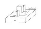
本発明に係るフィン型のFETの実施の第一形態は、図1に示すように、P型の伝導性を備えたシリコン(半導体)基板1上に、シリコン基板1上から外方に向かって突出してフィン形状に形成されたフィン部3、5を有する、金属−絶縁体−半導体のFETである。上記シリコン基板1の素材としては、半導体装置に使用できる半導体材料であればよく、例えば、ゲルマニウムや、シリコン−ゲルマニウムや、ガリウム−砒素といったものが挙げられる。また、上記フィン形状とは、シリコン基板1の表面方向に沿った水平断面が、帯状であり、かつ、シリコン基板1の表面方向に対し直交する方向の垂直断面が、帯状であるものをいう。(First embodiment)
As shown in FIG. 1, the first embodiment of the fin-type FET according to the present invention is formed on a silicon (semiconductor)
前記フィン部3、5には、チャネル領域部を長手方向の両側から挟んでソース領域部5およびドレイン領域部3が上記チャネル領域部の伝導性型と異なる、例えばN+形にてそれぞれ形成されている。さらに、上記チャネル領域部を被覆した、薄膜状のゲート誘電体8と、上記ゲート誘電体8によってチャネル領域部から絶縁されて、上記チャネル領域部上に形成されたゲート電極4とが形成されている。ゲート電極4は、上記チャネル領域部に対し跨ぐように形成されている。 In the
そして、本実施の第一形態では、上記シリコン基板1の表面上を覆う絶縁体層2が形成され、上記フィン部3、5が、上記シリコン基板1から上記絶縁体層2を貫通して上記絶縁体層2の表面より外方へ突出して延びるように形成されている。 In the first embodiment, the
これにより、上記構成は、フィン部3、5を、シリコン基板1から絶縁体層2を貫通して上記絶縁体層2の表面より突出して延びるように形成したから、上記フィン部3、5はシリコン基板1と直接接続されており、よって、チャネル領域部の本体がアース等の固定電位から浮いてしまうことに起因する、トランジスタ動作の不安定化を抑制できる。 Thereby, since the said structure formed the
また、上記構成は、チャネル領域部を含むフィン部3、5を、フィン形状に突出させて設けたことによって、高集積化のために微細化しても上記フィン部3、5の半導体材料が、トランジスタ動作状態において完全空乏化させることが可能となって、電気特性を向上できる。 In the above configuration, the
その上、上記構成は、シリコン基板1上を覆う絶縁体層2を設けたことによって、チャネル領域部の表面を覆う従来のSiN層の形成を省けるので、上記SiN層の形成による機械的な応力がチャネル領域部内に生成して漏電流を生じやすいという不都合も軽減できる。さらに、絶縁体層2の厚さを変化させれば、チャネル領域部の高さ(幅)を任意にて有するFIN−FETを製造できる。 In addition, the configuration described above eliminates the formation of the conventional SiN layer covering the surface of the channel region portion by providing the
本実施の第一形態においては、フィン部3、5(チャネル領域部)の幅は、上記絶縁体層2の表面より突出したフィン部3、5の高さの等倍から2倍までであることが好ましい。フィン部3、5のチャネル領域部は、シリコン基板1の表面に対して基本的には90度に近い角度を形成する少なくとも2つの互いにほぼ平行な各平坦面を備えていることが、高集積化のためには望ましい。 In the first embodiment, the width of the
上記の幅とは、フィン部3、5の長手方向(つまり、ドレイン領域部3、チャネル領域部およびソース領域部5が並ぶ方向)に対し直交し、かつシリコン基板1の表面方向に対し平行な方向の長さをいい、上記高さとは、フィン部3、5の長手方向に対し直交し、かつシリコン基板1の表面方向に対しても直交する方向の長さをいう。 The width is perpendicular to the longitudinal direction of the
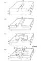
以下に、本実施の第一形態に係るFETの製造方法としての、バルクシリコンウエハ基板上でのFIN−FETおよびその製造方法について、図2(a)ないし図2(d)を参照して説明する。 Hereinafter, a FIN-FET on a bulk silicon wafer substrate and a method for manufacturing the same as a method for manufacturing an FET according to the first embodiment will be described with reference to FIGS. 2 (a) to 2 (d). To do.
まず、図2(a)に示すように、複数(図では一つのみ記載)の活性エリア10を、標準CMOSプロセス(フォトリソグラフィーとエッチング技術)とによって、例えば、バルクシリコンウエハ基板1’上にフィン形状に突出したように幅(W)にて形成した後、酸化膜等の誘電性絶縁部層2’を、各活性エリア10の先端部と面一となるように上記バルクシリコンウエハ基板1’上に堆積させて、上記誘電性絶縁部層2’内に埋め込んで上記各活性エリア10を規定する。各活性エリア10の埋め込みには、Siエッチングと、酸化と、CVDによる酸化物の充填と、化学機械研磨(CMP)による平坦化とを含む。 First, as shown in FIG. 2A, a plurality of active areas 10 (only one is shown in the figure) are formed on a bulk
次に、図2(b)に示すように、誘電性絶縁部層2'を厚さ方向にエッチバックして、浅いトレンチ分離(Shallow Trench Isolation; STI)を規定し、形成することによって、埋め込まれていたSiの各活性エリア10から、各フィン部3、5をそれぞれ形成するために露出させる。各フィン部3、5間は、エッチバックにより形成された浅いトレンチ分離である絶縁体層2によって絶縁されて規定されている。 Next, as shown in FIG. 2B, the dielectric insulating
通常、バルクシリコンウエハ基板1'上にある誘電性絶縁部層2'の深さ(D)は、活性エリア10の初期上面から300nm〜500nmである。上記活性エリア10の一部が露出するように誘電性絶縁部層2'をエッチバックしておく。残った絶縁体層2の厚みは、約150nm〜200nmであり、露出したフィン部3、5の高さ(H)は、150nm〜300nmである。しかし、上記高さは、エッチバックの量を調整することで任意に設計できる。 Usually, the depth (D) of the dielectric insulating
その後、上記FETのチャネル領域部となるフィン部3、5を、イオン注入(NMOSFETの場合はボロン)によってドープする。これにより、得られたFETの閾値電圧を決定できる。一般的に、上記チャネル領域部を、ドーピング濃度1×10¹⁶at/cm3〜1×1018at/cm3にてドープして形成する。上記チャネル領域部の幅は、ゲート電極4の幅に合わせればよいが、通常は、10nm〜300nmである。Thereafter, the
続いて、図2(c)に示すように、上記チャネル領域部となったフィン部3、5上に、ゲート誘電体8を熱成長または堆積により形成させる。ゲート誘電体(酸化物)8の有効な厚みは、2nm〜4nmの範囲である。 Subsequently, as shown in FIG. 2C, a
ゲート誘電体8の形成後、ゲート電極材料を上記絶縁体層2およびフィン部3、5上に堆積させて形成し、上記ゲート電極材料をパターン化して帯状のゲート電極4を形成する。ゲート電極4を、CVDポリシリコンを用いて形成してもよい。ゲート電極4を形成した後、上記ゲート電極4上を絶縁被覆(conformally covers)するように、上記ゲート電極4上に約3nmの厚さにてSiN層を堆積させる。 After the
次に、CVD酸化物を、堆積させ、エッチバックすることにより、図2(d)に示すように、ソース領域部5およびドレイン領域部3の各注入部7、6をゲート電極4の端部からオフセットするための側壁スペーサーを形成してもよい。ソース領域部5およびドレイン領域部3のためのN+注入部7、6は、約1×10²⁰at/cm3のドーピング濃度となるように注入されたAsイオンおよび/またはPイオンの組み合わせが好ましい。Next, CVD oxide is deposited and etched back, so that the
続いて、上記FETにおいては、中間段階誘電体(Inter-Level-Dielectric; ILD)堆積、導通用開口部、および、FETへの各接続部と各内部配線(interconnects)とを形成するための金属層の形成という従来のプロセスに従って本実施の第一形態のフィン型のFETが得られる。 Subsequently, in the FET, a metal for forming an intermediate-level dielectric (ILD) deposition, an opening for conduction, and each connection to the FET and each internal wiring (interconnects) The fin-type FET according to the first embodiment of the present invention is obtained in accordance with the conventional process of layer formation.
上記製造方法では、FETをバルクシリコンウエハ基板1’上に直接製造するので、フィン部3、5におけるのバルクシリコンウエハ基板1’との接触部は自動的に規定される。言い換えると、上記FETのチャネル領域部の本体は、P型のバルクシリコンウエハ基板1’と直接接触している。 In the above manufacturing method, since the FET is directly manufactured on the bulk
この構造では、フォトリソグラフィープロセスが、活性エリア10の幅を規定するから、チャネル領域部の幅の異なるFETを製造できる。活性エリア10からのフィン部3、5の高さとその幅とが同じ値(comparables)に設定すれば、バルクシリコンウエハ基板1’と直接接触している、トリゲートのフィン型のFETが得られる。 In this structure, since the photolithography process defines the width of the
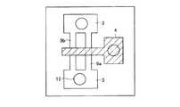
続いて、本実施の第一形態の一変形例を、図3および図4を参照して説明する。本変形例では、図3に示すように、図1に示すフィン部3、5が、その幅方向に分割された2つの各チャネル指状部9a、9bとなっている。各ソース領域部5およびドレイン領域部3においては、各コンタクト(導通)部12を形成してもよい。このようなフィン型FETでは、図4に示すように、各チャネル指状部9a、9bのチャネル領域11の幅(図2(a)にて示すW)を狭く設定でき、かつ、とドーピング濃度が十分に調節されている場合、ゲート電極4への電位の印加により、チャネル領域11の完全な空乏化が可能となる。 Subsequently, a modification of the first embodiment will be described with reference to FIGS. 3 and 4. In this modification, as shown in FIG. 3, the
(実施の第二形態)
本実施の第二形態では、図5に示すように、ソース領域部5およびドレイン領域部3が、絶縁体層2上において、その表面方向に沿って広がって延びているソース領域拡張部5aおよびドレイン領域拡張部3aを有している。このような実施の第二形態に係るFETの、バルクシリコンウエハ基板1’上での製造プロセスについて説明する。このFETの製造技術は、特に、ゲートアレイまたはメモリ装置などのトランジスタアレイの形成に好適に応用できる。また、バルクシリコンウエハ基板1’は、最終プロセスにて、必要に応じて分割されて、前記シリコン基板1となるものである。(Second embodiment)
In the second embodiment, as shown in FIG. 5, the
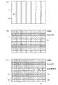
上記製造プロセスは、図2(b)に示す、FIN−FETのSi突出部であるフィン部3、5の形成について前述した方法と同じ方法から始まる。図6(a)に示すように、FIN−FETのアレイの場合には、バルクシリコンウエハ基板1’上に、帯状(ストライプ状)のSiの突出部であるフィン部21を、複数、互いに平行に、かつ等間隔にて形成する。 The above manufacturing process starts from the same method as described above for the formation of the
続いて、各フィン部21を形成した後、例えばCVDによる酸化物層24を堆積させ、CMP技術によってSiのフィン部21の高さに合わせて上記酸化物層24の表面を平坦化する。この平坦化に続いて、上記フィン部21および酸化物層24上に、SiN層22を、100nm〜200nmの厚さで堆積させる。このSiN層22を、フォトエッチング技術によってパターン化し、図6(b)に示すようなSiのフィン部21の長手方向に対して直交する方向の帯状に形成する。続いて、フォトレジストマスクで、FIN−FETの領域を被覆し、露出している酸化物層24を、異方性除去する。その結果、酸化物層24は、FIN−FETのチャネル領域部に沿った領域にのみダミー23として残る。 Subsequently, after each
次に、例えばSiH2ガスを使用してシリコンエピタキシー(Si−epi)成長をフィン部21に対して行う。SiN層22が、「天井(シーリング)」層として機能するので、SiN22の下側においてだけ側方エピタキシー成長が行われ、エピ(epi)成長部25が形成される。Next, for example, silicon epitaxy (Si-epi) growth is performed on the
このことを、図6(c)のA−A’の矢視断面図である図7(a)にて示す。露出しているエリア(断面B−B’)についてのシリコンエピタキシー成長を、図7(b)に示す。シリコンエピタキシー成長の後、図7(c)に記載のように、各フィン部21の先端から外方に突出した過剰なシリコンであるエピ(epi)成長部25をCMPの適用により除去する。この平坦化の後、酸化物であるダミー23とSiN層22とを除去する。 This is shown in FIG. 7A, which is a cross-sectional view taken along the line A-A 'in FIG. FIG. 7B shows the silicon epitaxy growth for the exposed area (cross section B-B ′). After the silicon epitaxy growth, as shown in FIG. 7C, the epi growth portion 25 which is excess silicon protruding outward from the tip of each
このプロセスの結果、図5に示すように、バルクシリコンウエハ基板1’との接合エリアは最小であり、絶縁体層2上においては広がったソース領域拡張部5aおよびドレイン領域拡張部3aをそれぞれ備えたソース領域部5およびドレイン領域部3がそれぞれ形成される。 As a result of this process, as shown in FIG. 5, the junction area with the bulk
これにより、ソース領域部5およびドレイン領域部3を絶縁体層2上にて広がるように形成することで、ソース領域部5/ドレイン領域部3の各コンタクト部を大きくできて外部との接合を容易化できる。 Thus, by forming the
その上、上記構成は、ソース領域部5/ドレイン領域部3の多くの部分を絶縁体層2上に形成でき、バルクシリコンウエハ基板1’と接触しているソース領域部5/ドレイン領域部3の各接合エリアを小さくできるから、寄生(接合)容量や放電を小さく維持できて、前述の寄生容量や放電の影響の低減を確実化できて、上記寄生容量や放電による特性劣化を回避できる。 In addition, the above configuration can form many portions of the
SiN層22を除去した後、続いて、本発明の製造プロセスでは、ゲート誘電体8の堆積または熱成長およびゲート電極4の形成を行う。図8は、この技術を使用したトランジスタアレイパターンを示す。残りのFET製造プロセスは、前記の本実施の第一形態で説明したような類似技術である。 After removing the SiN layer 22, subsequently, in the manufacturing process of the present invention, the
本発明のFIN−FET形成技術によって、以下の各効果を発揮できる。
1)バルクシリコンウエハ基板1'上にダブルゲートやトリゲートのFETの実現を簡便化できて、その結果、製造コストがより低くなる。
2)バルク制御されたバルクシリコンウエハ基板1'において完全空乏層を形成して動作するフィン型のFETを形成できる。その結果、閾値下の傾斜がほぼ理想的になり、OFF状態漏電流が低減される。それゆえ、上記FETを用いたLSIの待機電流を低くできる。
3)ソース領域部5およびドレイン領域部3の接合エリアを小さくできて、寄生容量と放電とが低減されて、上記寄生容量や放電による特性劣化を回避できる。The following effects can be exhibited by the FIN-FET formation technology of the present invention.
1) The realization of a double-gate or tri-gate FET on the bulk
2) A fin-type FET that operates by forming a fully depleted layer on a bulk-controlled bulk
3) The junction area between the
本発明のFETは、製造コストを低減しながら、高集積化できて、かつ特性劣化を抑制できるので、LSIなどの集積回路のメモリ装置やトランジスタアレイといった電子部品の用途に適用できる。 Since the FET of the present invention can be highly integrated and reduce characteristic deterioration while reducing the manufacturing cost, it can be applied to the use of an electronic component such as a memory device of an integrated circuit such as an LSI or a transistor array.
1 シリコン基板(半導体基板)
2 絶縁体層
3 ドレイン領域部(フィン部)
4 ゲート電極(フィン部)
5 ソース領域部(フィン部)
8 ゲート誘電体(ゲート誘電体薄膜)
1 Silicon substrate (semiconductor substrate)
2
4 Gate electrode (fin part)
5 Source region part (fin part)
8 Gate dielectric (gate dielectric thin film)
Claims (9)
Translated fromJapanese前記フィン部に、チャネル領域部と、チャネル領域部を挟んでそれぞれ形成されたソース領域部およびドレイン領域部と、
上記フィン部のチャネル領域部を被覆したゲート誘電体薄膜と、
上記ゲート誘電体薄膜によってチャネル領域部から絶縁されて、上記チャネル領域部上に形成されたゲート電極と、
上記半導体基板上を覆う絶縁体層とを含み、
上記フィン部は、上記半導体基板から上記絶縁体層を貫通して上記絶縁体層の表面より突出して延びるように形成され、
前記フィン部は、前記フィン部の幅方向に2つの各チャンネル指状部となっている、ことを特徴とする電界効果トランジスタ。A metal-insulator-semiconductor field-effect transistor having a fin portion protruding in a fin shape on a semiconductor substrate,
A channel region portion and a source region portion and a drain region portion formed on the fin portion with the channel region portion interposed therebetween,
A gate dielectric thin film covering the channel region portion of the fin portion;
A gate electrode formed on the channel region by being insulated from the channel region by the gate dielectric thin film;
Including an insulator layer covering the semiconductor substrate,
The fin portion is formed to extend from the semiconductor substrate through the insulator layer and project from the surface of the insulator layer,
2. The field effect transistor according toclaim 1, wherein the fin portion has two channel finger portions in the width direction of the fin portion .
Priority Applications (4)
| Application Number | Priority Date | Filing Date | Title |
|---|---|---|---|
| JP2004184182AJP4675585B2 (en) | 2004-06-22 | 2004-06-22 | Field effect transistor |
| KR1020050053378AKR100714775B1 (en) | 2004-06-22 | 2005-06-21 | Field effect transistor and fabrication method thereof |
| US11/157,077US7453124B2 (en) | 2004-06-22 | 2005-06-21 | Field effect transistor and fabrication method thereof |
| TW094120875ATWI281750B (en) | 2004-06-22 | 2005-06-22 | Field effect transistor and fabrication method thereof |
Applications Claiming Priority (1)
| Application Number | Priority Date | Filing Date | Title |
|---|---|---|---|
| JP2004184182AJP4675585B2 (en) | 2004-06-22 | 2004-06-22 | Field effect transistor |
Related Child Applications (1)
| Application Number | Title | Priority Date | Filing Date |
|---|---|---|---|
| JP2010242701ADivisionJP2011054985A (en) | 2010-10-28 | 2010-10-28 | Method of manufacturing field effect transistor |
Publications (2)
| Publication Number | Publication Date |
|---|---|
| JP2006012924A JP2006012924A (en) | 2006-01-12 |
| JP4675585B2true JP4675585B2 (en) | 2011-04-27 |
Family
ID=35481143
Family Applications (1)
| Application Number | Title | Priority Date | Filing Date |
|---|---|---|---|
| JP2004184182AExpired - Fee RelatedJP4675585B2 (en) | 2004-06-22 | 2004-06-22 | Field effect transistor |
Country Status (4)
| Country | Link |
|---|---|
| US (1) | US7453124B2 (en) |
| JP (1) | JP4675585B2 (en) |
| KR (1) | KR100714775B1 (en) |
| TW (1) | TWI281750B (en) |
Cited By (1)
| Publication number | Priority date | Publication date | Assignee | Title |
|---|---|---|---|---|
| US9536881B2 (en) | 2013-04-23 | 2017-01-03 | Samsung Electronics Co., Ltd. | Semiconductor devices having fin shaped channels |
Families Citing this family (49)
| Publication number | Priority date | Publication date | Assignee | Title |
|---|---|---|---|---|
| JP2006135067A (en)* | 2004-11-05 | 2006-05-25 | Toshiba Corp | Semiconductor device and manufacturing method thereof |
| US7525160B2 (en)* | 2005-12-27 | 2009-04-28 | Intel Corporation | Multigate device with recessed strain regions |
| US7838345B2 (en)* | 2006-05-02 | 2010-11-23 | Freescale Semiconductor, Inc. | Electronic device including semiconductor fins and a process for forming the electronic device |
| US7422960B2 (en)* | 2006-05-17 | 2008-09-09 | Micron Technology, Inc. | Method of forming gate arrays on a partial SOI substrate |
| US7678648B2 (en)* | 2006-07-14 | 2010-03-16 | Micron Technology, Inc. | Subresolution silicon features and methods for forming the same |
| JP4552908B2 (en)* | 2006-07-26 | 2010-09-29 | エルピーダメモリ株式会社 | Manufacturing method of semiconductor device |
| US7537994B2 (en) | 2006-08-28 | 2009-05-26 | Micron Technology, Inc. | Methods of forming semiconductor devices, assemblies and constructions |
| KR100772114B1 (en)* | 2006-09-29 | 2007-11-01 | 주식회사 하이닉스반도체 | Manufacturing method of semiconductor device |
| KR100858882B1 (en)* | 2007-03-19 | 2008-09-17 | 주식회사 하이닉스반도체 | Method of manufacturing transistor of semiconductor device |
| JP2008282901A (en)* | 2007-05-09 | 2008-11-20 | Sony Corp | Semiconductor device and manufacturing method of semiconductor device |
| KR100855834B1 (en)* | 2007-05-25 | 2008-09-01 | 주식회사 하이닉스반도체 | Semiconductor device and manufacturing method thereof |
| KR100870189B1 (en)* | 2007-05-28 | 2008-11-25 | 삼성전자주식회사 | Semiconductor device and manufacturing method thereof |
| JP2008300384A (en)* | 2007-05-29 | 2008-12-11 | Elpida Memory Inc | Semiconductor device and manufacturing method thereof |
| JP5069070B2 (en)* | 2007-09-27 | 2012-11-07 | ラピスセミコンダクタ株式会社 | Manufacturing method of semiconductor device |
| KR100943646B1 (en)* | 2007-12-28 | 2010-02-25 | 한국과학기술원 | Semiconductor memory device and manufacturing method thereof |
| US8022478B2 (en)* | 2008-02-19 | 2011-09-20 | International Business Machines Corporation | Method of forming a multi-fin multi-gate field effect transistor with tailored drive current |
| US7915659B2 (en)* | 2008-03-06 | 2011-03-29 | Micron Technology, Inc. | Devices with cavity-defined gates and methods of making the same |
| WO2010003928A2 (en)* | 2008-07-06 | 2010-01-14 | Interuniversitair Microelektronica Centrum Vzw (Imec) | Method for doping semiconductor structures and the semiconductor device thereof |
| JP2010040630A (en)* | 2008-08-01 | 2010-02-18 | Toshiba Corp | Semiconductor device |
| US8637135B2 (en) | 2009-11-18 | 2014-01-28 | Taiwan Semiconductor Manufacturing Company, Ltd. | Non-uniform semiconductor device active area pattern formation |
| US8445340B2 (en)* | 2009-11-19 | 2013-05-21 | Taiwan Semiconductor Manufacturing Company, Ltd. | Sacrificial offset protection film for a FinFET device |
| US8362572B2 (en)* | 2010-02-09 | 2013-01-29 | Taiwan Semiconductor Manufacturing Co., Ltd. | Lower parasitic capacitance FinFET |
| US8614134B2 (en)* | 2011-03-21 | 2013-12-24 | Globalfoundries Inc. | Shallow source and drain architecture in an active region of a semiconductor device having a pronounced surface topography by tilted implantation |
| CN104025293B (en)* | 2011-10-18 | 2018-06-08 | 英特尔公司 | Utilize the antifuse element of non-planar topology |
| KR20140113633A (en) | 2011-12-19 | 2014-09-24 | 소니 주식회사 | Solid-state image pickup device, manufacturing method for solid-state image pickup device, and electronic equipment |
| US10515956B2 (en) | 2012-03-01 | 2019-12-24 | Taiwan Semiconductor Manufacturing Company | Semiconductor devices having Fin Field Effect Transistor (FinFET) structures and manufacturing and design methods thereof |
| US9105744B2 (en) | 2012-03-01 | 2015-08-11 | Taiwan Semiconductor Manufacturing Company, Ltd. | Semiconductor devices having inactive fin field effect transistor (FinFET) structures and manufacturing and design methods thereof |
| US8629512B2 (en) | 2012-03-28 | 2014-01-14 | Taiwan Semiconductor Manufacturing Company, Ltd. | Gate stack of fin field effect transistor with slanted sidewalls |
| US20130264654A1 (en)* | 2012-04-06 | 2013-10-10 | Infineon Technologies Dresden Gmbh | Integrated Switching Device with Parallel Rectifier Element |
| US9012286B2 (en)* | 2012-04-12 | 2015-04-21 | Globalfoundries Inc. | Methods of forming FinFET semiconductor devices so as to tune the threshold voltage of such devices |
| US8664072B2 (en) | 2012-05-30 | 2014-03-04 | Globalfoundries Inc. | Source and drain architecture in an active region of a P-channel transistor by tilted implantation |
| US8697515B2 (en) | 2012-06-06 | 2014-04-15 | Taiwan Semiconductor Manufacturing Company, Ltd. | Method of making a FinFET device |
| US9209265B2 (en)* | 2012-11-15 | 2015-12-08 | Taiwan Semiconductor Manufacturing Company, Ltd. | ESD devices comprising semiconductor fins |
| KR101979637B1 (en) | 2012-11-26 | 2019-08-28 | 삼성전자주식회사 | Semiconductor device |
| US9812556B2 (en) | 2012-12-28 | 2017-11-07 | Renesas Electronics Corporation | Semiconductor device and method of manufacturing the semiconductor device |
| US9385069B2 (en)* | 2013-03-07 | 2016-07-05 | Taiwan Semiconductor Manufacturing Company, Ltd. | Gate contact structure for FinFET |
| US8940558B2 (en) | 2013-03-15 | 2015-01-27 | International Business Machines Corporation | Techniques for quantifying fin-thickness variation in FINFET technology |
| KR102030329B1 (en)* | 2013-05-30 | 2019-11-08 | 삼성전자 주식회사 | Semiconductor device and method for fabricating the same |
| JP2014241386A (en) | 2013-06-12 | 2014-12-25 | 富士通セミコンダクター株式会社 | Method for manufacturing semiconductor device and semiconductor device |
| CN105531797A (en)* | 2013-06-28 | 2016-04-27 | 英特尔公司 | Nanostructures and nanofeatures with Si(111) planes on Si(100) wafers for III-N epitaxy |
| US9263455B2 (en) | 2013-07-23 | 2016-02-16 | Micron Technology, Inc. | Methods of forming an array of conductive lines and methods of forming an array of recessed access gate lines |
| KR20150012837A (en)* | 2013-07-26 | 2015-02-04 | 에스케이하이닉스 주식회사 | 3 Dimension Semiconductor Device Having a lateral channel And Method of Manufacturing The same |
| CN104576380B (en) | 2013-10-13 | 2017-09-15 | 中国科学院微电子研究所 | FinFET manufacturing method |
| EP2889906B1 (en)* | 2013-12-30 | 2019-02-20 | IMEC vzw | Improvements in or relating to electrostatic discharge protection |
| EP3123521A4 (en)* | 2014-03-27 | 2017-10-25 | Intel Corporation | Confined epitaxial regions for semiconductor devices and methods of fabricating semiconductor devices having confined epitaxial regions |
| KR102327143B1 (en) | 2015-03-03 | 2021-11-16 | 삼성전자주식회사 | Integrated circuit device |
| US10084085B2 (en) | 2015-06-11 | 2018-09-25 | Taiwan Semiconductor Manufacturing Co., Ltd. | Fin field effect transistor (FinFET) device structure with stop layer and method for forming the same |
| US10466731B2 (en)* | 2016-01-27 | 2019-11-05 | Taiwan Semiconductor Manufacturing Co., Ltd. | Two-transistor bandgap reference circuit and FinFET device suited for same |
| US10367086B2 (en)* | 2017-06-14 | 2019-07-30 | Hrl Laboratories, Llc | Lateral fin static induction transistor |
Family Cites Families (18)
| Publication number | Priority date | Publication date | Assignee | Title |
|---|---|---|---|---|
| JP2851968B2 (en)* | 1991-04-26 | 1999-01-27 | キヤノン株式会社 | Semiconductor device having improved insulated gate transistor and method of manufacturing the same |
| US5604368A (en)* | 1994-07-15 | 1997-02-18 | International Business Machines Corporation | Self-aligned double-gate MOSFET by selective lateral epitaxy |
| JP3378414B2 (en)* | 1994-09-14 | 2003-02-17 | 株式会社東芝 | Semiconductor device |
| US5732014A (en)* | 1997-02-20 | 1998-03-24 | Micron Technology, Inc. | Merged transistor structure for gain memory cell |
| JP4384739B2 (en)* | 1997-04-04 | 2009-12-16 | 聯華電子股▲ふん▼有限公司 | Semiconductor device and manufacturing method thereof |
| US6252284B1 (en) | 1999-12-09 | 2001-06-26 | International Business Machines Corporation | Planarized silicon fin device |
| US20020011612A1 (en) | 2000-07-31 | 2002-01-31 | Kabushiki Kaisha Toshiba | Semiconductor device and method for manufacturing the same |
| JP2002118255A (en) | 2000-07-31 | 2002-04-19 | Toshiba Corp | Semiconductor device and manufacturing method thereof |
| JP4044276B2 (en)* | 2000-09-28 | 2008-02-06 | 株式会社東芝 | Semiconductor device and manufacturing method thereof |
| US6583469B1 (en)* | 2002-01-28 | 2003-06-24 | International Business Machines Corporation | Self-aligned dog-bone structure for FinFET applications and methods to fabricate the same |
| KR100458288B1 (en) | 2002-01-30 | 2004-11-26 | 한국과학기술원 | Double-Gate FinFET |
| US6642090B1 (en)* | 2002-06-03 | 2003-11-04 | International Business Machines Corporation | Fin FET devices from bulk semiconductor and method for forming |
| US7358121B2 (en)* | 2002-08-23 | 2008-04-15 | Intel Corporation | Tri-gate devices and methods of fabrication |
| JP2004214413A (en)* | 2002-12-27 | 2004-07-29 | Toshiba Corp | Semiconductor device |
| KR100471189B1 (en)* | 2003-02-19 | 2005-03-10 | 삼성전자주식회사 | Field effect transistors having a vertical channel and methods of fabricating the same |
| KR100476940B1 (en)* | 2003-06-20 | 2005-03-16 | 삼성전자주식회사 | Dram memory cell having a gate channel extending vertically from a substrate and method of fabricating the same |
| JPWO2005122272A1 (en)* | 2004-06-08 | 2008-04-10 | 日本電気株式会社 | MIS field effect transistor with strained silicon channel layer |
| JP2014110963A (en)* | 2013-10-28 | 2014-06-19 | Sanyo Product Co Ltd | Game machine |
- 2004
- 2004-06-22JPJP2004184182Apatent/JP4675585B2/ennot_activeExpired - Fee Related
- 2005
- 2005-06-21KRKR1020050053378Apatent/KR100714775B1/ennot_activeExpired - Lifetime
- 2005-06-21USUS11/157,077patent/US7453124B2/ennot_activeExpired - Lifetime
- 2005-06-22TWTW094120875Apatent/TWI281750B/ennot_activeIP Right Cessation
Cited By (1)
| Publication number | Priority date | Publication date | Assignee | Title |
|---|---|---|---|---|
| US9536881B2 (en) | 2013-04-23 | 2017-01-03 | Samsung Electronics Co., Ltd. | Semiconductor devices having fin shaped channels |
Also Published As
| Publication number | Publication date |
|---|---|
| JP2006012924A (en) | 2006-01-12 |
| KR20060046490A (en) | 2006-05-17 |
| US7453124B2 (en) | 2008-11-18 |
| KR100714775B1 (en) | 2007-05-04 |
| TW200625646A (en) | 2006-07-16 |
| US20050282342A1 (en) | 2005-12-22 |
| TWI281750B (en) | 2007-05-21 |
Similar Documents
| Publication | Publication Date | Title |
|---|---|---|
| JP4675585B2 (en) | Field effect transistor | |
| US7700446B2 (en) | Virtual body-contacted trigate | |
| US7394116B2 (en) | Semiconductor device including a multi-channel fin field effect transistor including protruding active portions and method of fabricating the same | |
| KR100585178B1 (en) | A semiconductor device comprising a metal FET having a metal gate electrode, and a manufacturing method thereof | |
| CN100448023C (en) | Semiconductor device with U-shaped grid structure | |
| KR100781580B1 (en) | Dual structure fin field effect transistor and its manufacturing method | |
| CN102668093B (en) | Contact with the circulating type of three gated devices for fin FETs | |
| JP5409997B2 (en) | Method for forming a gate in a FinFET device and method for manufacturing a semiconductor device | |
| US7385237B2 (en) | Fin field effect transistors with low resistance contact structures | |
| US8486788B2 (en) | Semiconductor device and method for fabricating the same | |
| KR100618893B1 (en) | Semiconductor device and manufacturing method | |
| US20060088967A1 (en) | Finfet transistor process | |
| KR100657969B1 (en) | A manufacturing method of a semiconductor device having a single gate electrode corresponding to a pair of pin-type channel regions | |
| JP2005086024A (en) | Semiconductor device and method for manufacturing same | |
| JP5925740B2 (en) | Tunnel field effect transistor | |
| JP2009038201A (en) | Semiconductor device and manufacturing method of semiconductor device | |
| WO2004073044A2 (en) | Finfet device and method to make same | |
| JP2006505949A (en) | Planarization of gate materials to improve the critical dimensions of semiconductor device gates. | |
| US8350269B2 (en) | Semiconductor-on-insulator (SOI) structure and method of forming the SOI structure using a bulk semiconductor starting wafer | |
| US20060216880A1 (en) | FINFET devices and methods of fabricating FINFET devices | |
| CN103579004B (en) | Finfet and manufacturing method thereof | |
| JP2009004425A (en) | Semiconductor device and manufacturing method of semiconductor device | |
| US9825094B2 (en) | FinFET PCM access transistor having gate-wrapped source and drain regions | |
| JP2011066362A (en) | Semiconductor device | |
| US20230246033A1 (en) | Fin field effect transistor with merged drift region |
Legal Events
| Date | Code | Title | Description |
|---|---|---|---|
| A621 | Written request for application examination | Free format text:JAPANESE INTERMEDIATE CODE: A621 Effective date:20060912 | |
| A977 | Report on retrieval | Free format text:JAPANESE INTERMEDIATE CODE: A971007 Effective date:20080724 | |
| A131 | Notification of reasons for refusal | Free format text:JAPANESE INTERMEDIATE CODE: A131 Effective date:20100615 | |
| A521 | Request for written amendment filed | Free format text:JAPANESE INTERMEDIATE CODE: A523 Effective date:20100804 | |
| RD02 | Notification of acceptance of power of attorney | Free format text:JAPANESE INTERMEDIATE CODE: A7422 Effective date:20100804 | |
| A131 | Notification of reasons for refusal | Free format text:JAPANESE INTERMEDIATE CODE: A131 Effective date:20100831 | |
| A521 | Request for written amendment filed | Free format text:JAPANESE INTERMEDIATE CODE: A523 Effective date:20101028 | |
| A131 | Notification of reasons for refusal | Free format text:JAPANESE INTERMEDIATE CODE: A131 Effective date:20101116 | |
| TRDD | Decision of grant or rejection written | ||
| A01 | Written decision to grant a patent or to grant a registration (utility model) | Free format text:JAPANESE INTERMEDIATE CODE: A01 Effective date:20110125 | |
| A01 | Written decision to grant a patent or to grant a registration (utility model) | Free format text:JAPANESE INTERMEDIATE CODE: A01 | |
| A61 | First payment of annual fees (during grant procedure) | Free format text:JAPANESE INTERMEDIATE CODE: A61 Effective date:20110126 | |
| FPAY | Renewal fee payment (event date is renewal date of database) | Free format text:PAYMENT UNTIL: 20140204 Year of fee payment:3 | |
| R150 | Certificate of patent or registration of utility model | Ref document number:4675585 Country of ref document:JP Free format text:JAPANESE INTERMEDIATE CODE: R150 | |
| R250 | Receipt of annual fees | Free format text:JAPANESE INTERMEDIATE CODE: R250 | |
| R250 | Receipt of annual fees | Free format text:JAPANESE INTERMEDIATE CODE: R250 | |
| R250 | Receipt of annual fees | Free format text:JAPANESE INTERMEDIATE CODE: R250 | |
| S111 | Request for change of ownership or part of ownership | Free format text:JAPANESE INTERMEDIATE CODE: R313113 | |
| R350 | Written notification of registration of transfer | Free format text:JAPANESE INTERMEDIATE CODE: R350 | |
| R250 | Receipt of annual fees | Free format text:JAPANESE INTERMEDIATE CODE: R250 | |
| R250 | Receipt of annual fees | Free format text:JAPANESE INTERMEDIATE CODE: R250 | |
| R250 | Receipt of annual fees | Free format text:JAPANESE INTERMEDIATE CODE: R250 | |
| R250 | Receipt of annual fees | Free format text:JAPANESE INTERMEDIATE CODE: R250 | |
| R250 | Receipt of annual fees | Free format text:JAPANESE INTERMEDIATE CODE: R250 | |
| LAPS | Cancellation because of no payment of annual fees |