JP4674382B1 - Inspection apparatus and defect inspection method - Google Patents
Inspection apparatus and defect inspection methodDownload PDFInfo
- Publication number
- JP4674382B1 JP4674382B1JP2010088445AJP2010088445AJP4674382B1JP 4674382 B1JP4674382 B1JP 4674382B1JP 2010088445 AJP2010088445 AJP 2010088445AJP 2010088445 AJP2010088445 AJP 2010088445AJP 4674382 B1JP4674382 B1JP 4674382B1
- Authority
- JP
- Japan
- Prior art keywords
- step bunching
- differential interference
- epitaxial layer
- image
- detection means
- Prior art date
- Legal status (The legal status is an assumption and is not a legal conclusion. Google has not performed a legal analysis and makes no representation as to the accuracy of the status listed.)
- Expired - Fee Related
Links
- 230000007547defectEffects0.000titleclaimsabstractdescription256
- 238000007689inspectionMethods0.000titleclaimsabstractdescription115
- 238000000034methodMethods0.000titleclaimsdescription28
- 239000000758substrateSubstances0.000claimsabstractdescription181
- 230000003287optical effectEffects0.000claimsabstractdescription95
- 238000012545processingMethods0.000claimsabstractdescription54
- 238000010008shearingMethods0.000claimsabstractdescription47
- 230000008859changeEffects0.000claimsabstractdescription23
- 238000001514detection methodMethods0.000claimsdescription115
- 239000013078crystalSubstances0.000claimsdescription56
- 238000005286illuminationMethods0.000claimsdescription40
- 230000002708enhancing effectEffects0.000claimsdescription5
- 238000003384imaging methodMethods0.000claimsdescription5
- 230000002194synthesizing effectEffects0.000claimsdescription4
- 230000001427coherent effectEffects0.000claimsdescription3
- 230000001105regulatory effectEffects0.000claimsdescription3
- HBMJWWWQQXIZIP-UHFFFAOYSA-Nsilicon carbideChemical compound[Si+]#[C-]HBMJWWWQQXIZIP-UHFFFAOYSA-N0.000description71
- 229910010271silicon carbideInorganic materials0.000description71
- 230000035945sensitivityEffects0.000description12
- 238000004519manufacturing processMethods0.000description10
- 230000008569processEffects0.000description9
- 230000004048modificationEffects0.000description5
- 238000012986modificationMethods0.000description5
- 239000013307optical fiberSubstances0.000description5
- 230000010287polarizationEffects0.000description5
- 239000004065semiconductorSubstances0.000description5
- 238000010586diagramMethods0.000description3
- 238000001914filtrationMethods0.000description3
- 230000006870functionEffects0.000description3
- QSHDDOUJBYECFT-UHFFFAOYSA-NmercuryChemical compound[Hg]QSHDDOUJBYECFT-UHFFFAOYSA-N0.000description3
- 229910052753mercuryInorganic materials0.000description3
- 238000012360testing methodMethods0.000description3
- 230000008901benefitEffects0.000description2
- 230000002950deficientEffects0.000description2
- 238000003908quality control methodMethods0.000description2
- 238000002310reflectometryMethods0.000description2
- 244000000626Daucus carotaSpecies0.000description1
- 235000002767Daucus carotaNutrition0.000description1
- 230000015572biosynthetic processEffects0.000description1
- 230000015556catabolic processEffects0.000description1
- 238000003708edge detectionMethods0.000description1
- 230000000694effectsEffects0.000description1
- 238000000605extractionMethods0.000description1
- 239000006210lotionSubstances0.000description1
- 229910052751metalInorganic materials0.000description1
- 239000002184metalSubstances0.000description1
- 238000007517polishing processMethods0.000description1
- 210000001747pupilAnatomy0.000description1
- 238000000790scattering methodMethods0.000description1
- 229910052710siliconInorganic materials0.000description1
- 239000010703siliconSubstances0.000description1
- 238000012546transferMethods0.000description1
- 238000002834transmittanceMethods0.000description1
- 229910052724xenonInorganic materials0.000description1
- FHNFHKCVQCLJFQ-UHFFFAOYSA-Nxenon atomChemical compound[Xe]FHNFHKCVQCLJFQ-UHFFFAOYSA-N0.000description1
Images


Landscapes
- Investigating Materials By The Use Of Optical Means Adapted For Particular Applications (AREA)
- Testing Or Measuring Of Semiconductors Or The Like (AREA)
Abstract
Translated fromJapaneseDescription
Translated fromJapanese本発明は、ステップフロー成長により形成されたエピタキシャル層の欠陥を検出する検査装置、特にエピタキシャル層に存在するステップバンチングとステップバンチング以外の格子欠陥等とを個別に検出できる検査装置に関するものである。 The present invention relates to an inspection apparatus that detects defects in an epitaxial layer formed by step flow growth, and more particularly to an inspection apparatus that can individually detect step bunching and lattice defects other than step bunching existing in an epitaxial layer.
単結晶基板上にエピタキシャル成長法により単結晶層を形成し、形成された単結晶層にデバイスを形成する半導体デバイスの製造方法が開発されている。この半導体デバイスの製造方法では、単結晶基板としてオフ角を有する炭化珪素基板が用いられ、ステップフロー成長によりエピタキシャル層が形成されている。炭化珪素は、シリコンと比較して、優れた物理的及び熱的特性を有するため、炭化珪素基板上に炭化珪素のエピタキシャル層が形成された半導体基体を用いたデバイスの製造方法は、高電力で低損失の半導体デバイスの製造に極めて有用である。 A semiconductor device manufacturing method has been developed in which a single crystal layer is formed on a single crystal substrate by an epitaxial growth method, and a device is formed on the formed single crystal layer. In this semiconductor device manufacturing method, a silicon carbide substrate having an off-angle is used as a single crystal substrate, and an epitaxial layer is formed by step flow growth. Since silicon carbide has superior physical and thermal characteristics compared to silicon, a method for manufacturing a device using a semiconductor substrate in which an epitaxial layer of silicon carbide is formed on a silicon carbide substrate is high power. This is extremely useful for manufacturing low-loss semiconductor devices.
上述した半導体デバイスの製造方法において、製造上の歩留りを改良しデバイスの信頼性を改善するためには、基板上に形成されたエピタキシャル層に存在する欠陥を検出することが重要である。従来、炭化珪素基板(SiC基板)に存在する欠陥を光学的に検出する方法として、レーザ散乱方式の欠陥検査装置が既知である(例えば、特許文献1参照)。このレーザ散乱方式の欠陥検査装置では、レーザダイオードから放出されたレーザ光をステージ上に配置された基板表面に対して斜めに入射させ、基板表面で発生した散乱光を光検出器により検出している。走査方法として、基板を支持するステージを回転させ、レーザビームを半径方向に移動させながら、基板の全面が走査されている。 In the semiconductor device manufacturing method described above, it is important to detect defects present in the epitaxial layer formed on the substrate in order to improve the manufacturing yield and improve the reliability of the device. Conventionally, a laser scattering type defect inspection apparatus is known as a method for optically detecting defects present in a silicon carbide substrate (SiC substrate) (see, for example, Patent Document 1). In this laser scattering type defect inspection apparatus, laser light emitted from a laser diode is obliquely incident on the surface of a substrate placed on a stage, and scattered light generated on the surface of the substrate is detected by a photodetector. Yes. As a scanning method, the entire surface of the substrate is scanned while rotating the stage that supports the substrate and moving the laser beam in the radial direction.
さらに、SiC基板の表面を微分干渉顕微鏡を用いて撮像し、欠陥の微分干渉画像から欠陥の種別を判定することも報告されている。微分干渉顕微鏡は、試料表面の高さ変化を位相差情報として検出するため、SiC基板表面に出現した微少な凹凸変化を輝度画像として検出できる利点がある。
ステップフロー成長によりエピタキシャル層が形成される単結晶基板においては、エピタキシャル層の成長中にオリフラと直交する方向に延在する線状の欠陥であるステップバンチングが多数形成される。このステップバンチングは、ステップフロー成長によりエピタキシャル層を形成する際不可避的に発生する。一方、マイクロパイプ欠陥や基底面内欠陥等の格子欠陥(結晶欠陥)とステップバンチングとは、その発生要因が異なるため、格子欠陥をステップバンチングと区別して検出することが望まれている。しかしながら、エピタキシャル層には多数のステップバンチングが形成されるため、エピタキシャル層表面の画像情報に基づいて欠陥検出を行う場合、マイクロパイプ欠陥等の格子欠陥をステップバンチングと区別して検出することは極めて煩雑である。 In a single crystal substrate on which an epitaxial layer is formed by step flow growth, many step bunchings, which are linear defects extending in a direction perpendicular to the orientation flat, are formed during the growth of the epitaxial layer. This step bunching inevitably occurs when an epitaxial layer is formed by step flow growth. On the other hand, lattice defects (crystal defects) such as micropipe defects and defects in the basal plane, and step bunching have different generation factors. Therefore, it is desired to detect lattice defects separately from step bunching. However, since many step bunchings are formed in the epitaxial layer, it is extremely complicated to detect lattice defects such as micropipe defects separately from step bunching when performing defect detection based on image information on the surface of the epitaxial layer. It is.
一方、ステップバンチングは、デバイスの酸化膜耐圧不良の原因となるため、エピタキシャル層のステップバンチングを検出することもデバイスの製造上の歩留りを改善する上で重要である。特に、ステップバンチングの分布密度と格子欠陥の発生分布とは相関性が認められることも報告されており、ステップバンチングの分布密度を測定することは、デバイスの製造の歩留りを改善する上で極めて重要である。また、SiC基板表面のステップバンチングの分布密度が検出されれば、ステップバンチングの少ない領域又はステップバンチングが形成されていない領域を選択してデバイスの製造に用いることができ、SiC基板の品質を管理する上で有益な情報が得られると共にデバイスの信頼性を高める上でも有益である。 On the other hand, since step bunching causes a breakdown voltage failure of the oxide film of the device, detection of the step bunching of the epitaxial layer is also important for improving the manufacturing yield of the device. In particular, it has been reported that there is a correlation between the distribution density of step bunching and the occurrence distribution of lattice defects, and measuring the distribution density of step bunching is extremely important for improving the manufacturing yield of devices. It is. Also, if the distribution density of step bunching on the surface of the SiC substrate is detected, it is possible to select a region with little step bunching or a region where no step bunching is formed and use it for device manufacturing, and control the quality of the SiC substrate. In addition, useful information can be obtained and the reliability of the device can be improved.
レーザ散乱方式の欠陥検査装置は、基板表面で発生した散乱光を検出しているので、基板表面に出現した欠陥を検出することが可能である。しかしながら、不所望な散乱光が光検出器に入射するため、欠陥検出の解像度が低く、微細な欠陥を検出しにくい欠点がある。特に、レーザ散乱方式の検査装置は、試料表面の高さ方向の検出感度が低いため、SiC基板の表面に形成された数nm〜数10nm程度の微少な凹凸状の欠陥を明瞭に検出しにくい欠点がある。また、レーザ散乱方式の欠陥検査装置では、単一のレーザビームを用いてエピタキシャル層表面をスパイラル状に走査しているため、ステップバンチングと格子欠陥とを区別して検出することができず、しかも、ステップバンチングに対してレーザビームが直交する場合と平行な場合とが交錯し、基板の位置によって欠陥検出の感度が安定しない欠点がある。さらに、SiC基板は可視域において透明であるため、照射されたレーザ光が基板の内部を通過し、基板の裏面で反射して基板表面から出射する。よって、基板の裏面からの反射光の影響を除去する必要がある。 Since the laser scattering type defect inspection apparatus detects scattered light generated on the substrate surface, it is possible to detect defects appearing on the substrate surface. However, since undesired scattered light is incident on the photodetector, the defect detection resolution is low and it is difficult to detect fine defects. In particular, the laser scattering type inspection apparatus has low detection sensitivity in the height direction of the sample surface, so that it is difficult to clearly detect minute unevenness defects of several nm to several tens of nm formed on the surface of the SiC substrate. There are drawbacks. Further, in the laser scattering type defect inspection apparatus, since the surface of the epitaxial layer is scanned in a spiral shape using a single laser beam, step bunching and lattice defects cannot be distinguished and detected, There is a disadvantage that the sensitivity of defect detection is not stable depending on the position of the substrate because the case where the laser beam is orthogonal to the step bunching and the case where the laser beam is parallel are crossed. Furthermore, since the SiC substrate is transparent in the visible region, the irradiated laser light passes through the substrate, is reflected by the back surface of the substrate, and is emitted from the substrate surface. Therefore, it is necessary to remove the influence of the reflected light from the back surface of the substrate.
微分干渉顕微鏡を用いて欠陥を検出する方法は、基板表面の微少な凹凸形状を輝度画像として検出できる利点がある。しかしながら、SiC基板は可視域において透明であるため、SiC基板を透過し、基板の裏面からの反射光が光検出器に入射するため、解像度が低下する問題点も指摘されている。 The method of detecting a defect using a differential interference microscope has an advantage that a minute uneven shape on the substrate surface can be detected as a luminance image. However, since the SiC substrate is transparent in the visible range, it has been pointed out that the resolution is lowered because the SiC substrate transmits the reflected light from the back surface of the substrate and enters the photodetector.
本発明の目的は、格子欠陥とステップバンチングとを分けて、ステップバンチングが検出されない態様で欠陥検出を行うことができる検査装置を実現することにある。 An object of the present invention is to realize an inspection apparatus capable of performing defect detection in a manner in which step bunching is not detected by separating lattice defects and step bunching.
本発明の別の目的は、格子欠陥等のステップバンチング以外の欠陥とステップバンチングとを個別に検出できる欠陥検査方法及び検査装置を実現することにある。
さらに、本発明の別の目的は、ステップバンチングとそれ以外の欠陥とを同時並行して検出できる検査装置を提供することにある。Another object of the present invention is to realize a defect inspection method and inspection apparatus that can individually detect defects other than step bunching such as lattice defects and step bunching.
Furthermore, another object of the present invention is to provide an inspection apparatus capable of detecting step bunching and other defects in parallel.
本発明による欠陥検査方法は、単結晶基板上にステップフロー成長により形成されたエピタキシャル層表面を微分干渉光学系を含む光学装置により撮像し、撮像された微分干渉画像に基づき単結晶基板に形成されたエピタキシャル層に存在する欠陥を検出する欠陥検査方法であって、
検査されるべき単結晶基板をステージ上に配置する工程と、
ステージの光軸周りの回転角度又は微分干渉光学系のシャーリング方向を調整して、微分干渉光学系のシャーリング方向をステージ上に配置された単結晶基板のエピタキシャル層に形成されたステップバンチングの延在方向と平行になるように設定する工程と、
微分干渉光学系を含む光学装置により、エピタキシャル層表面を撮像してステップバンチングが光学的に除去された微分干渉画像を形成する工程と、
形成された微分干渉画像に基づいて、欠陥検出を行う工程とを具えることを特徴とする。In the defect inspection method according to the present invention, an epitaxial layer surface formed by step flow growth on a single crystal substrate is imaged by an optical device including a differential interference optical system, and the single crystal substrate is formed based on the captured differential interference image. A defect inspection method for detecting defects existing in an epitaxial layer,
Placing a single crystal substrate to be inspected on a stage;
Extension of step bunching formed on the epitaxial layer of the single crystal substrate arranged on the stage by adjusting the rotation angle around the optical axis of the stage or the shearing direction of the differential interference optical system. A step of setting it to be parallel to the direction;
Imaging the surface of the epitaxial layer with an optical device including a differential interference optical system to form a differential interference image in which step bunching is optically removed; and
And a step of performing defect detection based on the formed differential interference image.
微分干渉光学系を含む検査装置では、検査される基板の表面高さの変化により2本のサブビーム間に生ずる位相差を検出して、輝度情報として出力している。従って、2本のサブビームを結ぶ方向(シャーリング方向)にそって基板の表面高さが一様な場合、2本のサブビーム間に位相差が形成されず、正常な部位の輝度画像と同様な輝度画像が形成される。一方、ステップバンチングは、オリフラの方向と直交する方向に延在する線状の段差であり、ほぼ全てのステップバンチングは互いに平行に形成される。また、ステップバンチングの高さは、その延在方向に沿ってほぼ一様な高さである。従って、微分干渉光学系のシャーリング方向を、ステップバンチングの延在方向と平行になるように設定して走査を行えば、2本のサブビーム間に位相差が発生せず、ステップバンチングが光学的に検出されない状態が形成される。一方、マイクロパイプ欠陥、基底面内欠陥、刃状転位欠陥等の格子欠陥は、微分干渉画像上ほぼ点状の輝度画像として検出される。また、キャロット欠陥やコメット欠陥等は特有の形状を有する欠陥であり、微分干渉画像上特有の形状の輝度画像として検出される。従って、微分干渉光学系のシャーリング方向をステップバンチングの延在方向と平行に設定してエピタキシャル層表面を走査すれば、ステップバンチングに対して検出感度が無い状態で欠陥検出を行うことができ、ステップバンチングを除く欠陥だけを選択して検出することが可能になる。この結果、発生頻度の高いステップバンチングによる影響を受けない欠陥検出が可能になる。 In an inspection apparatus including a differential interference optical system, a phase difference generated between two sub beams due to a change in the surface height of a substrate to be inspected is detected and output as luminance information. Therefore, when the surface height of the substrate is uniform along the direction connecting the two sub beams (shearing direction), no phase difference is formed between the two sub beams, and the same luminance as the luminance image of the normal part. An image is formed. On the other hand, step bunching is a linear step extending in a direction orthogonal to the orientation flat direction, and almost all step bunchings are formed in parallel to each other. The height of the step bunching is substantially uniform along the extending direction. Therefore, if scanning is performed with the shearing direction of the differential interference optical system set parallel to the extending direction of the step bunching, no phase difference occurs between the two sub-beams, and the step bunching is optically performed. An undetected state is formed. On the other hand, lattice defects such as micropipe defects, basal plane defects, and edge dislocation defects are detected as substantially point-like luminance images on the differential interference image. Carrot defects, comet defects, and the like are defects having a specific shape, and are detected as luminance images having a specific shape on the differential interference image. Therefore, if the shearing direction of the differential interference optical system is set parallel to the extending direction of the step bunching and the surface of the epitaxial layer is scanned, defect detection can be performed with no detection sensitivity with respect to the step bunching. Only defects other than bunching can be selected and detected. As a result, it becomes possible to detect a defect that is not affected by step bunching with a high occurrence frequency.
また、光学的にステップバンチングが除去されているので、欠陥検出工程において2次元の画像処理を用いて欠陥抽出を行うことができる。この結果、ステップバンチングを画像処理によって除去する方法に比べて、高感度に欠陥を検出することが可能である。さらに、画像処理によりステップバンチングを除去する場合、ステップバンチングの形成方向と角度が僅かに異なる方向に延在する線状の欠陥も画像処理により除去され或いはコントラストが低下してしまう。これに対して、当該方法では、微分干渉光学系のシャーリング方向以外の方向に延在する線状の欠陥は除去されないため、ステップバンチング方向と近い近似する方向に延在する線状の欠陥も明瞭に検出できる効果がある。 Further, since step bunching is optically removed, defect extraction can be performed using two-dimensional image processing in the defect detection process. As a result, it is possible to detect a defect with higher sensitivity than in the method of removing step bunching by image processing. Further, when step bunching is removed by image processing, linear defects extending in a direction slightly different from the step bunching forming direction are also removed by image processing or the contrast is lowered. In contrast, in this method, linear defects extending in directions other than the shearing direction of the differential interference optical system are not removed, and therefore linear defects extending in an approximate direction close to the step bunching direction are also clear. There is an effect that can be detected.
本発明による検査装置は、単結晶基板上にステップフロー成長により形成されたエピタキシャル層に存在するステップバンチング及びステップバンチング以外の欠陥を個別に検出する検査装置であって、
照明ビームを発生する光源装置と、前記照明ビームを集束した光ビームとして検査すべき単結晶基板のエピタキシャル層に向けて投射する対物レンズと、検査すべき単結晶基板を支持する移動可能なステージであって、対物レンズと直交する面内で回転可能なステージと、規制された光入射面を有し、前記単結晶基板のエピタキシャル層表面で反射した反射光を受光する光検出手段とを有し、ステージ移動又はビーム走査によりエピタキシャル層表面を走査する共焦点走査装置、
前記共焦点走査装置の対物レンズと光検出手段との間の光路中に配置され、入射した照明ビームを、互いに干渉性を有する第1及び第2のサブビームに変換すると共に、前記単結晶基板のエピタキシャル層表面で反射したサブビーム同士を合成し、エピタキシャル層表面の高さと関連する位相差情報を含む干渉ビームを出射させる微分干渉光学系、及び、
前記光検出手段から出力される輝度信号を受け取り、前記エピタキシャル層表面の共焦点微分干渉画像を形成する手段と、形成された共焦点微分干渉画像に基づいてステップバンチング以外の欠陥を検出する第1の欠陥検出手段と、前記共焦点微分干渉画像に基づいてエピタキシャル層表面に形成されたステップバンチングを検出する第2の欠陥検出手段とを有する信号処理装置を具え、
前記基板を支持するステージの光軸周りの回転角度又は前記微分干渉光学系のシャーリング方向は調整可能に設定され、
当該検査装置は、ステップバンチングを除く欠陥を検出する第1の検査モードと、ステップバンチングを検出する第2の検査モードとを有し、
前記第1の検査モードにおいて、ステージ上に配置した基板のステップバンチングの延在方向と微分干渉光学系のシャーリング方向とが互いに平行になるように設定され、前記第1の欠陥検出手段により欠陥検出が行われ、第2の検査モードにおいて、前記基板のステップバンチングの延在方向と微分干渉光学系のシャーリング方向とが平行以外の状態に設定され、前記第2の欠陥検出手段によりステップバンチングの検出が行われることを特徴とする。An inspection apparatus according to the present invention is an inspection apparatus that individually detects defects other than step bunching and step bunching existing in an epitaxial layer formed by step flow growth on a single crystal substrate,
A light source device that generates an illumination beam, an objective lens that projects the illumination beam toward an epitaxial layer of a single crystal substrate to be inspected as a focused light beam, and a movable stage that supports the single crystal substrate to be inspected A stage rotatable in a plane perpendicular to the objective lens, and a light detecting means having a regulated light incident surface and receiving reflected light reflected by the epitaxial layer surface of the single crystal substrate. A confocal scanning device for scanning the surface of the epitaxial layer by moving the stage or scanning the beam,
In the optical path between the objective lens of the confocal scanning device and the light detection means, the incident illumination beam is converted into first and second sub beams having coherence with each other, and A differential interference optical system for synthesizing sub-beams reflected on the surface of the epitaxial layer and emitting an interference beam including phase difference information related to the height of the surface of the epitaxial layer; and
First means for receiving a luminance signal output from the light detection means and forming a confocal differential interference image on the surface of the epitaxial layer and detecting defects other than step bunching based on the formed confocal differential interference image And a signal processing device having second defect detection means for detecting step bunching formed on the surface of the epitaxial layer based on the confocal differential interference image,
The rotation angle around the optical axis of the stage supporting the substrate or the shearing direction of the differential interference optical system is set to be adjustable,
The inspection apparatus has a first inspection mode for detecting defects other than step bunching, and a second inspection mode for detecting step bunching.
In the first inspection mode, the step bunching extension direction of the substrate placed on the stage and the shearing direction of the differential interference optical system are set to be parallel to each other, and the first defect detection means detects the defect. In the second inspection mode, the step bunching extension direction of the substrate and the shearing direction of the differential interference optical system are set to a state other than parallel, and step bunching is detected by the second defect detection means. Is performed.
本発明による検査装置は、ステップバンチングが光学的に検出されない第1の検査モードと、ステップバンチングが光学的に検出される第2の検査モードとを有するので、格子欠陥等の欠陥の検出とステップバンチングの検出とを個別に行うことが可能となる。尚、微分干渉光学系のシャーリング方向をステージ上に配置された基板表面のステップバンチングの延在方向に平行する設定する調整は、基板を支持するステージを光軸まわりで回転させ、又は微分干渉光学系のシャーリング方向を回転調整することにより行うことができる。第1の検査モードと第2の検査モードとの切り換えも同様である。 Since the inspection apparatus according to the present invention has a first inspection mode in which step bunching is not optically detected and a second inspection mode in which step bunching is optically detected, detection of defects such as lattice defects and steps are performed. Bunching can be detected separately. Note that the adjustment for setting the shearing direction of the differential interference optical system to be parallel to the extending direction of the step bunching on the surface of the substrate disposed on the stage is performed by rotating the stage supporting the substrate around the optical axis or by differential interference optics. This can be done by adjusting the shearing direction of the system. The same applies to switching between the first inspection mode and the second inspection mode.
検出されたステップバンチングの分布密度の表示方法として、検査される基板を複数の区域に分割し、各区域ごとに検出されたステップバンチングの本数を直接表示し、又は階調性を有する濃淡画像として表示することができる。このように、ステップバンチングの分布密度を計測することにより、基板全体についてステップバンチングの無い区域又はステップバンチングの密度が低い区域を選択することができ、良品のSiC基板により構成されるチイップだけを選択することが可能になる。 As a method of displaying the distribution density of the detected step bunching, the substrate to be inspected is divided into a plurality of areas, and the number of detected step bunchings is directly displayed for each area, or as a grayscale image having gradation. Can be displayed. In this way, by measuring the distribution density of step bunching, it is possible to select the area without step bunching or the area with low step bunching density for the entire substrate, and select only the chip composed of non-defective SiC substrates. It becomes possible to do.
共焦点走査装置として、単一の照明ビームを走査装置により走査し、単結晶基板表面からの反射光をピンホールを介して光検出手段により受光する共焦点走査装置、ライン状の照明ビームを走査装置又はステージ移動により走査し、単結晶基板からの反射光をリニアイメージセンサにより受光する共焦点走査装置、及び、ライン状に配列されたマルチビームを用いて単結晶基板を走査し、基板表面からの反射光をリニアイメージセンサにより受光する共焦点走査装置を用いることが可能である。 As a confocal scanning device, a single illumination beam is scanned by the scanning device, and the reflected light from the surface of the single crystal substrate is received by the light detection means through the pinhole, and the line-shaped illumination beam is scanned. Scanning a single crystal substrate using a multi-beam arranged in a line, and a confocal scanning device that scans by moving the device or stage and receives reflected light from the single crystal substrate by a linear image sensor, and from the substrate surface It is possible to use a confocal scanning device that receives the reflected light of the light by a linear image sensor.
本発明による別の検査装置は、単結晶基板上にステップフロー成長により形成されたエピタキシャル層に存在するステップバンチング及びステップバンチング以外の欠陥を個別に検出する検査装置であって、
照明ビームを発生する光源装置と、前記照明ビームを集束した光ビームとして検査すべき単結晶基板のエピタキシャル層に向けて投射する対物レンズと、検査すべき単結晶基板を支持する移動可能なステージと、規制された光入射面を有し、前記単結晶基板のエピタキシャル層表面で反射した反射光を受光する光検出手段とを有し、ステージ移動又はビーム走査によりエピタキシャル層表面を走査する共焦点走査装置、
前記共焦点走査装置の対物レンズと光検出手段との間の光路中に配置され、入射した照明ビームを、互いに干渉性を有する第1及び第2のサブビームに変換すると共に、前記単結晶基板のエピタキシャル層表面で反射したサブビーム同士を合成し、エピタキシャル層表面の高さと関連する位相差情報を含む干渉ビームを出射させる微分干渉光学系、及び、
前記光検出手段から出力される輝度信号を受け取り、前記エピタキシャル層表面の共焦点微分干渉画像を形成する手段と、形成された共焦点微分干渉画像に基づいてステップバンチング以外の欠陥を検出する第1の欠陥検出手段と、前記共焦点微分干渉画像に基づいてエピタキシャル層表面に形成されたステップバンチングを検出する第2の欠陥検出手段とを有する信号処理装置を具え、
前記第1の欠陥検出手段は、共焦点微分干渉画像に含まれるステップバンチング画像の延在方向と直交する方向の輝度変化を減衰させる手段を有し、
前記第2の欠陥検出手段は、前記共焦点微分干渉画像に含まれるステップバンチング画像の延在方向と直交する方向の輝度変化を強調する手段を有することを特徴とする。Another inspection apparatus according to the present invention is an inspection apparatus for individually detecting defects other than step bunching and step bunching existing in an epitaxial layer formed by step flow growth on a single crystal substrate,
A light source device that generates an illumination beam; an objective lens that projects the illumination beam toward an epitaxial layer of a single crystal substrate to be inspected as a focused light beam; and a movable stage that supports the single crystal substrate to be inspected A confocal scanning having a regulated light incident surface and having a light detecting means for receiving reflected light reflected by the epitaxial layer surface of the single crystal substrate, and scanning the epitaxial layer surface by stage movement or beam scanning apparatus,
In the optical path between the objective lens of the confocal scanning device and the light detection means, the incident illumination beam is converted into first and second sub beams having coherence with each other, and A differential interference optical system for synthesizing sub-beams reflected on the surface of the epitaxial layer and emitting an interference beam including phase difference information related to the height of the surface of the epitaxial layer; and
First means for receiving a luminance signal output from the light detection means and forming a confocal differential interference image on the surface of the epitaxial layer and detecting defects other than step bunching based on the formed confocal differential interference image And a signal processing device having second defect detection means for detecting step bunching formed on the surface of the epitaxial layer based on the confocal differential interference image,
The first defect detection means includes means for attenuating a luminance change in a direction orthogonal to the extending direction of the step bunching image included in the confocal differential interference image,
The second defect detecting means includes means for enhancing a luminance change in a direction orthogonal to the extending direction of the step bunching image included in the confocal differential interference image.
ステップバンチングの検出とステップバンチング以外の欠陥の検出とは、画像処理により行うことも可能である。すなわち、ステップバンチング及びそれ以外の欠陥の両方が検出される検査モードで走査して微分干渉画像を形成し、形成された微分干渉画像を、ステップバンチングの延在方向と直交する方向の輝度変化を減衰させる画像処理手段を有する第1の欠陥検出手段及びステップバンチングの延在方向と直交する方向の輝度変化を強調する画像処理を行う手段を有する第2の欠陥検出手段にそれぞれ供給する。第1の欠陥検出手段では、ステップバンチングが除去された画像情報について欠陥検出が行われ、第2の欠陥検出手段ではステップバンチングが強調された画像について欠陥検出が行われるので、ステップバンチングの検出とそれ以外の欠陥の検出とを同時並行して実行することが可能になる。尚、光検出手段として、TDIセンサやCCDセンサ等のイメージセンサを用いることができる。 Detection of step bunching and detection of defects other than step bunching can also be performed by image processing. That is, a differential interference image is formed by scanning in an inspection mode in which both step bunching and other defects are detected, and the formed differential interference image is subjected to a luminance change in a direction perpendicular to the extending direction of step bunching. The first defect detection means having an image processing means for attenuation and the second defect detection means having a means for performing image processing for emphasizing a luminance change in a direction orthogonal to the extending direction of the step bunching are supplied to the first defect detection means. In the first defect detection means, defect detection is performed on image information from which step bunching has been removed, and in the second defect detection means, defect detection is performed on an image in which step bunching is emphasized. It becomes possible to execute the detection of other defects simultaneously in parallel. An image sensor such as a TDI sensor or a CCD sensor can be used as the light detection means.
本発明による別の検査装置は、単結晶基板上にステップフロー成長により形成されたエピタキシャル層に存在するステップバンチング及びステップバンチング以外の欠陥を個別に検出する検査装置であって、
紫外域の波長光の照明ビームを発生する光源装置と、
前記照明ビームを検査すべき単結晶基板のエピタキシャル層に向けて投射する対物レンズと、
検査すべき単結晶基板を支持する移動可能なステージと、
前記単結晶基板のエピタキシャル層表面で反射した反射光を受光する光検出手段と、
前記対物レンズと光検出手段との間の光路中に配置され、入射した照明ビームを、互いに干渉性を有する第1及び第2のサブビームに変換すると共に、前記単結晶基板のエピタキシャル層表面で反射したサブビーム同士を合成し、エピタキシャル層表面の高さと関連する位相差情報を含む干渉ビームを出射させる微分干渉光学系と、
前記光検出手段から出力される輝度信号を受け取り、前記エピタキシャル層表面の微分干渉画像を形成する手段、形成された微分干渉画像に基づいてステップバンチング以外の欠陥を検出する第1の欠陥検出手段、及び、前記微分干渉画像に基づいてエピタキシャル層表面に形成されたステップバンチングを検出する第2の欠陥検出手段を有する信号処理装置とを具え、
前記基板を支持するステージの光軸周りの回転角度又は前記微分干渉光学系のシャーリング方向は調整可能に設定され、
当該検査装置は、ステップバンチングを除く欠陥を検出する第1の検査モードと、ステップバンチングを検出する第2の検査モードとを有し、
前記第1の検査モードにおいて、ステージ上に配置した基板のステップバンチングの延在方向と微分干渉光学系のシャーリング方向とが互いに平行になるように設定されて前記第1の欠陥検出手段により欠陥検出が行われ、第2の検査モードにおいて、前記基板のステップバンチングの延在方向と微分干渉光学系のシャーリング方向とが平行以外の状態に設定されて前記第2の欠陥検出手段によりステップバンチングの検出が行われることを特徴とする。Another inspection apparatus according to the present invention is an inspection apparatus for individually detecting defects other than step bunching and step bunching existing in an epitaxial layer formed by step flow growth on a single crystal substrate,
A light source device that generates an illumination beam of light in the ultraviolet region;
An objective lens that projects the illumination beam toward an epitaxial layer of a single crystal substrate to be inspected;
A movable stage that supports the single crystal substrate to be inspected;
A light detecting means for receiving the reflected light reflected by the surface of the epitaxial layer of the single crystal substrate;
An incident illumination beam, which is disposed in the optical path between the objective lens and the light detection means, converts the incident illumination beam into first and second sub-beams that are coherent with each other, and is reflected on the surface of the epitaxial layer of the single crystal substrate. A differential interference optical system that synthesizes the sub-beams and emits an interference beam including phase difference information related to the height of the epitaxial layer surface;
Means for receiving a luminance signal output from the light detection means and forming a differential interference image on the surface of the epitaxial layer; first defect detection means for detecting defects other than step bunching based on the formed differential interference image; And a signal processing device having second defect detection means for detecting step bunching formed on the surface of the epitaxial layer based on the differential interference image,
The rotation angle around the optical axis of the stage supporting the substrate or the shearing direction of the differential interference optical system is set to be adjustable,
The inspection apparatus has a first inspection mode for detecting defects other than step bunching, and a second inspection mode for detecting step bunching.
In the first inspection mode, the step bunching extension direction of the substrate disposed on the stage and the shearing direction of the differential interference optical system are set to be parallel to each other, and defect detection is performed by the first defect detection means. In the second inspection mode, the step bunching extension direction of the substrate and the shearing direction of the differential interference optical system are set to a state other than parallel, and step bunching is detected by the second defect detection means. Is performed.
SiC基板の裏面からの反射光の影響を除去するため、共焦点走査装置を用いる代りに、光源を適切に選択することにより裏面からの反射光の影響を除去することも可能である。すなわち、SiC基板は、紫外域の波長光に対して不透明であるため、照明光源として、紫外域の波長光を放出する光源を用いる。この場合、SiC基板の裏面からの反射光が発生しないため、共焦点走査装置ではなくても、高い解像度の微分干渉画像を撮像することが可能である。 In order to remove the influence of the reflected light from the back surface of the SiC substrate, it is possible to remove the influence of the reflected light from the back surface by appropriately selecting a light source instead of using the confocal scanning device. That is, since the SiC substrate is opaque to ultraviolet wavelength light, a light source that emits ultraviolet wavelength light is used as the illumination light source. In this case, since no reflected light is generated from the back surface of the SiC substrate, it is possible to capture a high-resolution differential interference image without using the confocal scanning device.
本発明によれば、微分干渉光学系のシャーリング方向を調整し又は基板を支持するステージの回転角度を調整することにより、光学的にステップバンチングが検出されない状態で欠陥検出を行うことができるので、ステップバンチングとこれ以外の欠陥とを個別に検出することが可能である。
また、ステップバンチングを検出する欠陥検出手段とステップバンチング以外の欠陥を検出する欠陥検出手段を有することにより、画像処理によってステップバンチングの検出と格子欠陥の検出とを個別に同時並行して行うことができる。According to the present invention, by adjusting the shearing direction of the differential interference optical system or adjusting the rotation angle of the stage that supports the substrate, defect detection can be performed in a state in which step bunching is not optically detected. It is possible to individually detect step bunching and other defects.
Also, by having defect detection means for detecting step bunching and defect detection means for detecting defects other than step bunching, step bunching detection and lattice defect detection can be performed individually and in parallel by image processing. it can.
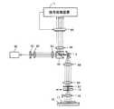
図1は本発明による検査装置の一例を示す線図である。本例では、検査すべき単結晶基板としてエピタキシャル層が形成された炭化珪素基板(SiC基板)を用いる。勿論、単結晶基板として、SiC基板だけでなく、ステップフロー成長によりエピタキシャル層が形成された各種の単結晶基板の検査を行うことができる。検査装置として、微分干渉光学系を有する共焦点走査装置を用い、共焦点走査装置により炭化珪素基板の全面を走査して基板全面の共焦点微分干渉画像を撮像する。得られた共焦点微分干渉画像について種々の画像処理を行って欠陥及びその座標(アドレス)を検出すると共にステップバンチングの分布密度も計測する。微分干渉光学系は、試料表面の高さの変化を走査光の位相差の変化として検出するので、数nm〜数10nm程度の凹状及び凸状の欠陥を輝度変化として検出することが可能である。 FIG. 1 is a diagram showing an example of an inspection apparatus according to the present invention. In this example, a silicon carbide substrate (SiC substrate) on which an epitaxial layer is formed is used as a single crystal substrate to be inspected. Of course, not only a SiC substrate but also various single crystal substrates on which an epitaxial layer is formed by step flow growth can be inspected as a single crystal substrate. A confocal scanning device having a differential interference optical system is used as the inspection device, and the entire surface of the silicon carbide substrate is scanned by the confocal scanning device to capture a confocal differential interference image on the entire surface of the substrate. Various image processing is performed on the obtained confocal differential interference image to detect the defect and its coordinates (address) and also measure the distribution density of the step bunching. Since the differential interference optical system detects a change in the height of the sample surface as a change in the phase difference of the scanning light, it is possible to detect a concave and convex defect of several nm to several tens of nm as a luminance change. .
図1を参照するに、照明光源1として、水銀ランプを用いる。尚、キセノンランプ等の水銀ランプ以外の種々の照明光源も用いることができる。照明光源1から出射した照明ビームは、複数の光ファイバが円形に積層された光ファイババンドル2に入射し、光ファイバを伝搬して、断面がほぼ円形の発散性ビームとして出射し、フィルタ3に入射する。フィルタ3は、入射した光ビームから緑の波長光(e線:波長546nm)を出射させる。フィルタから出射した光ビームは、集束性レンズ4により平行ビームに変換されてスリット5に入射する。スリット5は、集束性レンズ4の瞳位置に配置され、第1の方向(紙面と直交する方向)に延在する細長い開口部を有する。ここで、第1の方向は、X方向と称する。スリット5の開口部の幅は、例えば10〜20μmに設定する。従って、スリット5から第1の方向に延在する細長いライン状の光ビームが出射する。スリット5から出射したライン状の光ビームは、偏光子6に入射し、単一の振動面を持つ偏光した光に変換される。このライン状の偏光ビームは、ビームスプリッタとして機能するハーフミラー7で反射し、リレーレンズ8を経て走査装置として機能する振動ミラー9に入射する。 Referring to FIG. 1, a mercury lamp is used as the illumination light source 1. Various illumination light sources other than mercury lamps such as xenon lamps can also be used. The illumination beam emitted from the illumination light source 1 is incident on an optical fiber bundle 2 in which a plurality of optical fibers are stacked in a circle, propagates through the optical fiber, and is emitted as a divergent beam having a substantially circular cross section. Incident. The filter 3 emits green wavelength light (e-line: wavelength 546 nm) from the incident light beam. The light beam emitted from the filter is converted into a parallel beam by the converging lens 4 and enters the slit 5. The slit 5 is disposed at the pupil position of the converging lens 4 and has an elongated opening extending in a first direction (a direction orthogonal to the paper surface). Here, the first direction is referred to as the X direction. The width of the opening of the slit 5 is set to 10 to 20 μm, for example. Therefore, an elongated line-shaped light beam extending in the first direction is emitted from the slit 5. The linear light beam emitted from the slit 5 enters the polarizer 6 and is converted into polarized light having a single vibration surface. This line-shaped polarized beam is reflected by the half mirror 7 that functions as a beam splitter, and enters a vibrating mirror 9 that functions as a scanning device via a relay lens 8.
振動ミラー9には、駆動回路10が接続され、駆動回路10は信号処理装置11から供給される制御信号に基づき振動ミラーを駆動する。振動ミラー9は、入射するライン状の光ビームを第1の方向と直交する第2の方向(Y方向)に偏向する。信号処理装置11は、振動ミラーの角度情報に基づいて、光ビームのY方向の位置情報を有する。尚、振動ミラーは、ステップアンドリピートにより欠陥検出を行う場合に使用され、或いは、欠陥をレビューするに用いられる。従って、基板を支持するステージを移動させて基板を走査する場合、必ずしも必要ではない。振動ミラー9から出射したライン状の光ビームは、リレーレンズ12及び13を経て微分干渉光学系14に入射する。本例では、微分干渉光学系としてノマルスキープリズムを用いる。ノマルスキープリズム14に入射したライン状の偏光ビームは、振動面が互いに直交する2本のサブビームに変換される。これら2本のサブビーム間には、mを自然数とした場合に、(2m+1)π/2の位相差が与えられる。従って、SiC基板のエピタキシャル層表面に形成された数nmの高さ変化を有する欠陥を輝度画像として検出することが可能である。ノマルスキープリズム14にはモータ15が連結され、ノマルスキープリズムのシャーリング方向を自在に設定することができ、SiC基板に形成されたエピタキシャル層に存在するステップバンチングの延在方向に応じて、シャーリング方向を設定することができる。 A
ノマルスキープリズム14から出射した2本のサブビームは、対物レンズ16に入射する。対物レンズ16は、入射した2本のライン状のサブビームを集束し、ステージ17上に配置された観察すべき炭化珪素基板18のエピタキシャル層表面に向けて投射する。従って、SiC基板18の表面は、第1の方向(X方向)に延在するライン状の2本のサブビームにより、直交する第2の方向(Y方向)に走査される。 The two sub beams emitted from the
ステージ17は、X方向及びX方向と直交するY方向に移動可能なXYステージにより構成されると共に、対物レンズの光軸と直交する面内で回転可能なステージとする。ステージのX方向及びY方向の位置情報は、位置センサ(図示せず)により検出され、ステージの位置情報が信号処理装置11に供給される。また、ステージ17の回転角もセンサ(図示せず)により検出され、信号処理装置11に供給される。SiC基板18の全面を走査して欠陥を検出する場合、振動ミラー9を静止状態に維持し、ステージ17をY方向及びX方向にジッグザッグ状に移動させてSiC基板の全面を走査することができる。或いは、ステージ17を第1の方向に連続的に移動させ、振動ミラー9による第2の方向の走査と組み合わされて、SiC基板の全面について欠陥検査を行うこともできる。さらに、振動ミラーによる走査とステージ移動とを組み合わせたステップアンドリピートにより基板全面を走査するが可能である。尚、ステージ移動によりSiC基板の表面を走査する場合、ステージの移動方向とステップバンチングの延在方向とが平行になるように設定することが望ましい。また、検出された欠陥のアドレスを用いてレビューする場合、欠陥の座標情報に基づいてステージをX及びY方向に移動させて欠陥を視野内に位置させ、振動ミラーを第2の方向にスキャンすることにより欠陥及びその付近の共焦点微分干渉画像を撮像することができる。 The
対物レンズ16にはモータ19及びモータ駆動回路20が接続され、信号処理装置11から供給される駆動制御信号により光軸方向に沿って移動することができる。対物レンズの光軸方向の位置は位置センサ21により検出され、信号処理装置11に供給される。ここで、モータ19は、対物レンズとステージ上のSiC基板との間の光軸方向の相対距離、すなわち、基板表面を走査する光ビームの集束点と基板表面との間の相対距離を変化させる手段として機能する。尚、対物レンズは、10nmの分解能で光軸方向に移動することができる。 A
SiC基板の表面で反射した2本の反射ビームは、対物レンズ16により集光され、微分干渉光学系14に入射する。2本の反射サブビームは、微分干渉光学系14により合成され、SiC基板表面の高さ変化を位相差情報として含む干渉ビームが形成される。例えば、SiC基板の表面に数nm程度の凹状又は凸状の欠陥が存在する場合、SiC基板表面に入射した2本のサブビームのうち1本のサブが欠陥上を走査し、他方のサブビームは正常な表面部分を走査するので、2本のサブビーム間には欠陥の高さに応じた位相差が導入される。また、エピタキシャル層表面にステップバンチングが形成されている場合、高さが1nm程度のステップバンチングを線状の高輝度画像又は低輝度画像として検出することが可能である。この結果、微分干渉光学系14から出射する干渉ビームは、結晶欠陥に起因してSiC基板の表面に出現した数nm程度の凹凸変化やステップバンチングによる段差を位相差情報として含むことになる。 The two reflected beams reflected from the surface of the SiC substrate are collected by the
ノマルスキープリズム14から出射した干渉ビームは、元の光路を反対方向に伝搬し、リレーレンズ13及び12を経て振動ミラー9に入射し、振動ミラーによりデスキャンされる。振動ミラー9から出射した干渉ビームは、結像レンズとして作用するレンズ8を通過し、ハーフミラー7を透過し、検光子22に入射する。検光子22は、偏光子6に対して直交ニコルの関係に配置する。従って、ノマルスキープリズム14において合成された偏光以外の光は遮断され、微分干渉画像を構成する光だけが検光子22を透過する。 The interference beam emitted from the
検光子22を透過したライン状の干渉ビームは、ポジショナ23を経てリニアイメージセンサ24に入射する。リニアイメージセンサ24は、第1の方向と対応する方向に配列された複数の受光素子を有し、入射したライン状の干渉ビームを受光する。リニアイメージセンサの各受光素子は、干渉ビームに含まれる位相差情報を輝度情報に変換する。従って、SiC基板の表面又はエピタキシャル層の表面に形成された数nm程度の凹凸形状の欠陥及びステップバンチングは輝度画像として表示される。リニアイメージセンサのライン状に配列された受光素子列は、枠により入射開口が制限されているから、各受光素子の前面にピンホールが配置されているものとほぼ同等である。従って、SiC基板表面からの反射光をリニアイメージセンサにより受光することにより、微分干渉光学系を有する共焦点光学系が構成される。 The linear interference beam transmitted through the
リニアイメージセンサの各受光素子に蓄積された電荷は、信号処理装置11から供給される読出制御信号により順次読み出され、SiC基板表面の1次元画像信号として出力される。リニアイメージセンサから出力される1次元画像信号は、増幅器25で増幅され、カメラリンクを介して信号処理装置11に供給される。信号処理装置11は、画像処理ボードを有し、受け取った1次元画像信号、振動ミラーの位置情報、及びステージの位置情報等を用いてSiC基板表面の2次元画像を生成する。また、生成された2次元画像についてフィルタリング処理、2値化処理及び閾値比較処理を含む種々の画像処理を行って欠陥を検出すると共にその座標を取得する。ステップバンチングについては、格子欠陥等の他の欠陥から区別して検出することができる。 The electric charge accumulated in each light receiving element of the linear image sensor is sequentially read out by a read control signal supplied from the
SiC基板は、可視光の波長域において透明である。このため、SiC基板の表面を光ビームにより走査すると、入射した光ビームがSiC基板の内部を透過し、SiC基板の裏面で反射した反射光が検出器に入射し、解像度が低下する不都合がある。このため、微分干渉顕微鏡によりSiC基板を撮像する場合及びレーザ散乱方式により欠陥を検出する場合共に解像度が低く、欠陥検出の精度が低下する欠点がある。これに対して、本発明による共焦点型の検査装置では、リニアイメージセンサの前面にピンホールが配置されたものとほぼ等価な構成を有するので、SiC基板を透過し裏面で反射した光は、光路から外れリニアイメージセンサの受光素子に入射せず、SiC基板の表面で反射した反射光だけがリニアイメージセンサに入射する。この結果、本発明による検査装置を用いることにより、一般的な微分干渉顕微鏡により得られる微分干渉画像よりも高い解像度の共焦点微分干渉画像を撮像することができ、一層高い検出精度で欠陥検出を行うことが可能である。 The SiC substrate is transparent in the visible light wavelength range. For this reason, when the surface of the SiC substrate is scanned with a light beam, the incident light beam is transmitted through the inside of the SiC substrate, and the reflected light reflected from the back surface of the SiC substrate is incident on the detector, resulting in a decrease in resolution. . For this reason, both the case where the SiC substrate is imaged by the differential interference microscope and the case where the defect is detected by the laser scattering method have a drawback that the resolution is low and the accuracy of the defect detection is lowered. In contrast, the confocal inspection apparatus according to the present invention has a configuration that is substantially equivalent to a pinhole disposed on the front surface of the linear image sensor. Out of the optical path, it does not enter the light receiving element of the linear image sensor, but only the reflected light reflected by the surface of the SiC substrate enters the linear image sensor. As a result, by using the inspection apparatus according to the present invention, it is possible to capture a confocal differential interference image with a resolution higher than that of a differential interference image obtained by a general differential interference microscope, and detect defects with higher detection accuracy. Is possible.
微分干渉光学系は、試料表面に形成された数nm程度の微少な凹凸を位相差として検出するので、刃状転位欠陥や基底面内転位等の基板に存在する結晶欠陥に起因してエピタキシャル層表面に数nm程度の凹凸が形成されている場合、これらの凹凸を輝度画像として検出することが可能である。さらに、突起欠陥や凹状欠陥に関して、微分干渉画像上において、上向きの斜面及び下向きの斜面は低輝度画像又は高輝度画像として検出されるので、撮像された微分干渉画像に表示された明暗の輝度変化に基づいて凹状欠陥であるか又は凸状欠陥であるかも判別することが可能である。従って、撮像された明暗の微分干渉画像に基づいて、ピット欠陥であるか又はバンプ欠陥であるかも容易に判別することができる。 The differential interference optical system detects minute unevenness of about several nanometers formed on the sample surface as a phase difference, so that the epitaxial layer is caused by crystal defects existing on the substrate such as edge dislocation defects and dislocations in the basal plane. When unevenness of about several nm is formed on the surface, these unevenness can be detected as a luminance image. Furthermore, with respect to protrusion defects and concave defects, upward and downward slopes are detected as low-intensity images or high-intensity images on the differential interference image, so the brightness change between the brightness and darkness displayed in the captured differential interference image It is possible to determine whether the defect is a concave defect or a convex defect. Therefore, it is possible to easily determine whether the defect is a pit defect or a bump defect based on the captured bright and dark differential interference image.
さらに、ステップバンチングは、オリフラと直交する方向に延在し、高さが数nm〜数10nm程度の線状の段差欠陥である。従って、エピタキシャル層表面の共焦点微分干渉画像を撮像することにより、低度輝度(暗い)又は高輝度(明るい)の線状の輝度画像として検出される。尚、エピタキシャル層に格子欠陥とステップバンチングとの両方が形成されている場合、共焦点微分干渉画像上においては、点状の又は特有の形状の輝度画像と線状の輝度画像とが混在した形態として検出される。 Furthermore, the step bunching is a linear step defect extending in a direction orthogonal to the orientation flat and having a height of about several nanometers to several tens of nanometers. Therefore, by capturing a confocal differential interference image on the surface of the epitaxial layer, it is detected as a linear luminance image of low luminance (dark) or high luminance (bright). In the case where both lattice defects and step bunching are formed in the epitaxial layer, on the confocal differential interference image, a form in which a point-like or characteristic luminance image and a linear luminance image are mixed. Detected as
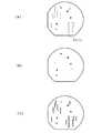
次に、SiC基板及びエピタキシャル層に形成される欠陥が、本発明による検査装置により撮像される共焦点微分干渉画像においていかなる形態のものとして撮像されるかについて説明する。
[ステップバンチング]
ステップバンチングは、サブnm〜数10nmのほぼ均一な高さの線状の段差である。SiC基板においては、格子欠陥の発生頻度に比べてはるかに大量のステップバンチングが形成され、ほとんどのステップバンチングは基板のオリフラと直交する方向に互いに平行に形成される。微分干渉光学系を含む共焦点走査装置で撮像した場合、微分干渉光学系のシャーリング方向に応じて明線又は暗線の輝度画像として検出される。
[マイクロパイプ欠陥]
マイクロパイプは中空孔の形態をした欠陥である。従って、走査ビームがマイクロパイプ欠陥上を走査した際、孔の底面からの反射光がリニアイメージセンサに入射せず又は微少光量の反射光しか入射しないため、点状の低輝度画像として検出される。
[異物付着]
表面に異物が付着した場合、金属等の反射率の高い異物が付着した場合点状の高輝度画像として検出され、反射率の低い異物が付着した場合点状の暗い低輝度画像として検出される。
[ダウンフォール]
ダウンフォールは、エピタキシャル層の成長中に塊がエピタキシャル層上に付着することにより形成され、上向き及び下向きの2つの傾斜面を有する形態をとる。よって、微分干渉画像として撮像した場合、明るい画像部分と暗い画像部分とが結合した明暗の輝度画像として検出される。
[刃状転位欠陥]
刃状転位欠陥は、SiC基板又はエピタキシャル層の表面上においてピット構造として出現する。従って、下向き及び上向きの2つの傾斜面を有する形態であり、微分干渉画像においては低輝度の画像部分と高輝度の画像部分とが結合した明暗の輝度画像として検出される。
[螺旋転位欠陥]
螺旋転位は、刃状転位欠陥と同様にSiC基板及びエピタキシャル層の表面においてピット構造として出現し、明暗の輝度画像として検出される。
[基底面内欠陥]
基底面内欠陥は、SiC基板の表面及びエピタキシャル層の表面において、ピット構造として出現する。従って、微分干渉画像において、明暗の輝度画像として検出される。
[バンプ]
バンプは、突起状の欠陥であり、下向きの斜面と上向きの斜面を有するので、明暗の輝度画像として検出される。
[スクラッチ]
基板の研磨処理中にスクラッチが形成される場合がある。このスクラッチは、線状の凹部構造であるので、共焦点微分干渉画像上線状の明暗の輝度画像として検出される。Next, it will be described in what form the defect formed in the SiC substrate and the epitaxial layer is captured in the confocal differential interference image captured by the inspection apparatus according to the present invention.
[Step bunching]
Step bunching is a linear step having a substantially uniform height from sub-nm to several tens of nm. In the SiC substrate, a much larger amount of step bunching is formed than the frequency of occurrence of lattice defects, and most step bunchings are formed in parallel to each other in a direction perpendicular to the orientation flat of the substrate. When an image is captured by a confocal scanning device including a differential interference optical system, it is detected as a bright line or dark line luminance image according to the shearing direction of the differential interference optical system.
[Micropipe defects]
Micropipes are defects in the form of hollow holes. Therefore, when the scanning beam scans over the micropipe defect, the reflected light from the bottom surface of the hole does not enter the linear image sensor or only a small amount of reflected light, so that it is detected as a dot-like low luminance image. .
[Foreign matter adhesion]
When a foreign object adheres to the surface, a foreign object with high reflectivity such as metal is detected as a dot-like high-intensity image, and when a foreign object with low reflectivity adheres, it is detected as a dot-like dark low-intensity image .
[Downfall]
The downfall is formed by a lump being deposited on the epitaxial layer during the growth of the epitaxial layer, and has a form having two inclined surfaces, upward and downward. Therefore, when it is captured as a differential interference image, it is detected as a bright and dark luminance image in which a bright image portion and a dark image portion are combined.
[Edge dislocation defects]
Edge dislocation defects appear as pit structures on the surface of the SiC substrate or epitaxial layer. Therefore, it has a form having two downward and upward inclined surfaces, and in the differential interference image, it is detected as a bright and dark luminance image in which the low luminance image portion and the high luminance image portion are combined.
[Spiral dislocation defects]
Similar to the edge dislocation defect, the screw dislocation appears as a pit structure on the surface of the SiC substrate and the epitaxial layer, and is detected as a bright and dark luminance image.
[Flaws in the basal plane]
The defects in the basal plane appear as pit structures on the surface of the SiC substrate and the surface of the epitaxial layer. Therefore, the differential interference image is detected as a bright and dark luminance image.
[bump]
A bump is a protrusion-like defect, and has a downward slope and an upward slope, and is thus detected as a bright and dark luminance image.
[scratch]
Scratches may be formed during the polishing process of the substrate. Since this scratch has a linear concave structure, it is detected as a linear bright and dark luminance image on the confocal differential interference image.
次に、本発明による欠陥検出方法について説明する。SiC基板のエピタキシャル層に形成されるステップバンチングの発生密度は、結晶欠陥や異物付着による欠陥よりもはるかに高い特性がある。従って、撮像されたエピタキシャル層表面の共焦点微分干渉画像から、格子欠陥や異物付着による欠陥を検出しようとすると、同時に検出されるステップバンチングの数が多過ぎ、格子欠陥等を検出することが煩雑になってしまう。従って、マイクロパイプ欠陥や基底面内欠陥等の格子欠陥を検出する場合、ステップバンチングが検出されない状態で欠陥検出を行うことが望ましい。他方において、ステップバンチングの分布密度は、基板の領域ないし部位に応じて相違し、エピタキシャル層中でステップバンチングが全く形成されない部位がある一方、ステップバンチングが高い密度で形成される部位もある。従って、基板上に形成されたエピタキシャル層について、ステップバンチングの分布密度が検出されれば、SiC基板の品質管理上有益が情報を得ることが可能であり、デバイスの製造の歩留りを改善する上で極めて有用な情報が得られる。 Next, the defect detection method according to the present invention will be described. The generation density of step bunching formed in the epitaxial layer of SiC substrate has characteristics that are much higher than those due to crystal defects and defects due to foreign matter adhesion. Therefore, when trying to detect a lattice defect or a defect due to adhesion of foreign matter from a confocal differential interference image of the surface of the epitaxial layer taken, too many step bunchings are detected at the same time, and it is complicated to detect the lattice defect or the like. Become. Therefore, when detecting a lattice defect such as a micropipe defect or a defect in the basal plane, it is desirable to detect the defect without detecting step bunching. On the other hand, the distribution density of step bunching differs depending on the region or part of the substrate, and there are parts where step bunching is not formed at all in the epitaxial layer, while there are parts where step bunching is formed at a high density. Therefore, if the distribution density of step bunching is detected for the epitaxial layer formed on the substrate, it is possible to obtain information useful for quality control of the SiC substrate, and to improve the device manufacturing yield. Very useful information can be obtained.
そこで、本発明による検査装置では、2つの検査モードを設定し、2つの検査モード間で切り換え可能に設定する。第1の検査モードは、マイクロパイプ欠陥や規定面内欠陥等の結晶欠陥や異物付着による欠陥等のステップバンチング以外の欠陥を検出するモードである。第2の検査モードは、ステップバンチングを他の欠陥と区別して検出し、ステップバンチングを積極的に検出するモードである。第1の検査モードでは、ステップバンチングの特性と微分干渉光学系の特性を考慮して、ステップバンチングだけが光学的に検出されない状態、すなわち、ステップバンチングに対してのみ検出感度が低下した検査状態を形成し、その状態で欠陥検出を行う。第2の検査モードでは、共焦点微分干渉画像上においてステップバンチングと他の欠陥の両方を検出し、ステップバンチングの特有の形状、すなわち一方向に延在する線状画像として撮像される特性に整合した画像処理、すなわち、ステップバンチングの延在方向の画像を強調する画像処理を行ってステップバンチングを他の欠陥と区別して検出する。 Therefore, in the inspection apparatus according to the present invention, two inspection modes are set and can be switched between the two inspection modes. The first inspection mode is a mode for detecting a defect other than step bunching such as a crystal defect such as a micropipe defect or a specified in-plane defect or a defect due to adhesion of foreign matter. The second inspection mode is a mode in which step bunching is detected separately from other defects and step bunching is positively detected. In the first inspection mode, in consideration of the characteristics of step bunching and the characteristics of the differential interference optical system, a state in which only step bunching is not optically detected, that is, an inspection state in which the detection sensitivity is reduced only for step bunching. Then, the defect is detected in that state. In the second inspection mode, both step bunching and other defects are detected on the confocal differential interference image and matched to the characteristic shape of the step bunching, that is, the characteristic captured as a linear image extending in one direction. The image processing, that is, the image processing for enhancing the image in the extending direction of the step bunching is performed to detect the step bunching separately from other defects.
2つの検査モードの設定方法について説明する。前述したように、ステップバンチングは、ほぼ均一な高さの線状の段差であり、ほぼ全てのステップバンチングは基板のオリフラの形成方向と直交する方向に延在する特性がある。また、微分干渉光学系の特性として、シャーリング方向に沿って試料表面の高さ変化がない場合、2本のサブビーム間に位相差は生じない。従って、ステップバンチングの延在方向と微分干渉光学系のシャーリング方向とを一致させて走査を行えば、2本のサブビーム間に位相差が発生せず、ステップバンチングに対してだけ検出感度が低下した検査状態が形成される。この検査状態は、微分干渉光学系のシャーリング方向又は基板を支持するステージの回転角度を調整する方法により設定することができる。例えば、ステージのX方向移動により主走査が行われ、微分干渉光学系のシャーリング方向が主走査方向すなわちX方向に設定されている場合、ステップバンチングの延在方向がX方向となるように、すなわちステップバンチングの延在方向がシャーリング方向と平行となるようにステージを回転調整する。この状態で走査を行えば、2本のサブビームは共にステップバンチング上を走査することになり、位相差が発生せず、ステップバンチングに対する検出感度が低下した検査状態が形成される。また、微分干渉光学系のシャーリング方向を調整することによりステップバンチングの検出感度を抑制するには、シャーリング方向をステージ上の基板のステップバンチングの延在方向と平行になるように調整することにより、ステップバンチングに対する検出感度が低下した検査状態が形成される。すなわち、微分干渉光学系のシャーリング方向又は基板を支持するステージの回転角度を調整することにより、ステップバンチングの検出感度を光学的に低下させることが可能になる。 A method for setting the two inspection modes will be described. As described above, step bunching is a linear step having a substantially uniform height, and almost all step bunching has a characteristic of extending in a direction orthogonal to the orientation flat formation direction of the substrate. Further, as a characteristic of the differential interference optical system, when there is no change in the height of the sample surface along the shearing direction, no phase difference occurs between the two sub beams. Therefore, if scanning is performed with the extending direction of the step bunching and the shearing direction of the differential interference optical system matched, no phase difference occurs between the two sub-beams, and the detection sensitivity is reduced only for the step bunching. An inspection state is formed. This inspection state can be set by a method of adjusting the shearing direction of the differential interference optical system or the rotation angle of the stage that supports the substrate. For example, when the main scanning is performed by moving the stage in the X direction and the shearing direction of the differential interference optical system is set to the main scanning direction, that is, the X direction, the extending direction of the step bunching is set to the X direction, that is, The stage is rotated and adjusted so that the extending direction of the step bunching is parallel to the shearing direction. If scanning is performed in this state, both of the two sub-beams scan on the step bunching, so that an inspection state is formed in which no phase difference occurs and the detection sensitivity to step bunching is lowered. Also, in order to suppress the detection sensitivity of step bunching by adjusting the shearing direction of the differential interference optical system, by adjusting the shearing direction to be parallel to the extending direction of the step bunching of the substrate on the stage, An inspection state in which the detection sensitivity to step bunching is reduced is formed. That is, by adjusting the shearing direction of the differential interference optical system or the rotation angle of the stage that supports the substrate, the detection sensitivity of step bunching can be optically reduced.
一方、ステップバンチングを積極的に検出する第2の検査モードでは、ステップバンチングが検出され易いように微分干渉光学系のシャーリング方向又はステージの回転角度を設定する。例えば、微分干渉光学系のシャーリング方向がステップバンチングの延在方向と直交するように微分干渉光学系のシャーリング方向又はステージの回転角度を調整すれば、ステップバンチングの明瞭な画像を撮像することができる。ただし、ステップバンチングの輝度画像は、ステップバンチングの延在方向とシャーリング方向とが平行な状態からずれるにしたがって周囲の画像との輝度差が大きくなり、ある角度を超えるとほぼ一定の輝度値の画像となる。従って、シャーリング方向とステップバンチングの延在方向とが互いに直交した状態で検査することが望ましいが、厳密に直交させる必要はなく、シャーリング方向とステップバンチングの延在方向とが平行な状態から外れた状態に設定して第2の検査モードを実行することが可能である。 On the other hand, in the second inspection mode in which step bunching is positively detected, the shearing direction of the differential interference optical system or the rotation angle of the stage is set so that step bunching is easily detected. For example, if the shearing direction of the differential interference optical system or the rotation angle of the stage is adjusted so that the shearing direction of the differential interference optical system is orthogonal to the extending direction of the step bunching, a clear image of step bunching can be captured. . However, the luminance image of step bunching increases in luminance difference from the surrounding images as the step bunching extension direction and shearing direction deviate from the parallel state, and an image having a substantially constant luminance value exceeds a certain angle. It becomes. Therefore, it is desirable to inspect in a state where the shearing direction and the extending direction of the step bunching are orthogonal to each other, but it is not necessary to strictly inspect, and the shearing direction and the extending direction of the step bunching are out of the parallel state. It is possible to set the state and execute the second inspection mode.
ここで、第1の検査モードにおける検査手法について説明する。エピタキシャル層に形成されたステップバンチングは、基板に形成されているオリフラの方向とほぼ直交する方向に延在する線状欠陥である。この点を考慮して、以下の手法を用いて欠陥検出を行う。初めに、ステージ上に基板を配置する。この際、ステージに対する基板の向きは、基板に形成されたオリフラにより規定される。続いて、ステージの光軸周りの回転角度を調整し、微分干渉光学系のシャーリング方向とステップバンチングの延在方向とが互いに平行になるように設定する。或いは、ステージを固定した状態で、微分干渉光学系のシャーリング方向をオリフラの方向と直交するように調整する。この状態で微分干渉画像の撮像を開始する。尚、基板の一部分について微分干渉画像を撮像し、ステップバンチングが除去されているかを確認し、ステップバンチングが残存する場合、ステージ又は微分干渉光学系を微調整して、ステップバンチングがほぼ完全に除去された状態に設定することも可能である。このように、オリフラを利用することにより、微分干渉光学系のシャーリング方向をステップバンチングの延在方向に平行に設定することが可能である。 Here, the inspection method in the first inspection mode will be described. Step bunching formed in the epitaxial layer is a linear defect extending in a direction substantially orthogonal to the direction of the orientation flat formed in the substrate. Considering this point, defect detection is performed using the following method. First, a substrate is placed on the stage. At this time, the orientation of the substrate with respect to the stage is defined by an orientation flat formed on the substrate. Subsequently, the rotation angle around the optical axis of the stage is adjusted and set so that the shearing direction of the differential interference optical system and the extending direction of the step bunching are parallel to each other. Alternatively, with the stage fixed, the shearing direction of the differential interference optical system is adjusted to be orthogonal to the orientation flat direction. In this state, imaging of the differential interference image is started. Take a differential interference image of a part of the substrate and check if step bunching has been removed. If step bunching remains, finely adjust the stage or differential interference optical system to remove step bunching almost completely. It is also possible to set to the state that has been set. Thus, by using the orientation flat, it is possible to set the shearing direction of the differential interference optical system parallel to the extending direction of the step bunching.
図2は、第1及び第2の検査モードにおいて撮像される共焦点微分干渉画像を模式的に示す図である。図2(A)は、SiC基板の表面の共焦点微分干渉画像を模式的に示す。格子欠陥や異物付着による欠陥は点状の輝度画像として観察され、ステップバンチングは、オリフラと直交する方向に延在する線状の輝度画像として観察される。図2(B)は、第1の検査モードにおいて観察される画像を示す。第1の検査モードでは、オリフラと直交する方向の検出感度が低減されているため、ほとんどのステップバンチングが消去され、格子欠陥等の欠陥画像だけが検出される。図2(C)は、ステップバンチングを強調した画像処理を行った画像を示す。オリフラと直交する方向の画像を強調する画像処理が行われているため、ステップバンチングの画像が強調された画像が得られる。 FIG. 2 is a diagram schematically illustrating a confocal differential interference image captured in the first and second inspection modes. FIG. 2 (A) schematically shows a confocal differential interference image of the surface of the SiC substrate. A lattice defect or a defect due to foreign matter adhesion is observed as a dot luminance image, and step bunching is observed as a linear luminance image extending in a direction orthogonal to the orientation flat. FIG. 2B shows an image observed in the first inspection mode. In the first inspection mode, since the detection sensitivity in the direction orthogonal to the orientation flat is reduced, most of the step bunching is erased and only defect images such as lattice defects are detected. FIG. 2C shows an image that has been subjected to image processing with emphasis on step bunching. Since image processing for emphasizing an image in a direction orthogonal to the orientation flat is performed, an image in which the step bunching image is enhanced is obtained.
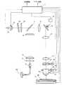
図3は、欠陥検出及びステップバンチングの分布密度検出を行う信号処理装置11の一例を示す線図である。本例では、第1の検査モードに設定して欠陥検出を行う。すなわち、ステップバンチングに対する検出感度が抑制された検査状態で検査が行われ、ステップバンチングが検出されない画像が撮像される。リニアイメージセンサ23から出力され、増幅器24により増幅された1次元画像信号は、A/D変換器30によりデジタル信号に変換され、信号処理装置11に供給される。また、基板を支持するステージ17の位置を示すステージ位置信号(デジタル信号)も信号処理装置11に供給する。本例では、信号処理装置11は、コンピュータにより実行されるソフトウェアで構成され、各種の手段は、制御手段31の制御のもとで動作するものとする。尚、制御手段31からの信号線は図面が交錯するため、図示しないものとする。 FIG. 3 is a diagram illustrating an example of the
信号処理装置11に入力した1次元画像信号は、2次元画像生成手段32に送られて2次元画像、すなわち2次元共焦点微分干渉画像が形成される。この2次元画像信号は第1の画像メモリ33に供給され、SiC基板のエピタキシャル層が形成された全面の共焦点微分干渉画像が第1の画像メモリ33に蓄積される。第1の画像メモリ33に記憶されている画像は、ステップバンチングが光学的に除去された画像である。2次元画像生成手段32により形成された2次元画像信号は第1の欠陥検出手段34に供給される。第1の欠陥検出手段34には、ステージ位置信号及びリニアイメージセンサの各受光素子の位置情報も供給される。第1の欠陥検出手段34は、フィルタリング手段、2値化手段及び閾値比較手段を含み、入力した2次元画像について画像処理を行って欠陥を検出する。同時に、ステージ位置信号及びリニアイメージセンサの各受光素子の位置情報を用いて、検出された欠陥の座標も取得する。検出された欠陥の座標は、第1の欠陥メモリ35に記憶する。 The one-dimensional image signal input to the
SiC基板に形成された欠陥を観察する場合、制御手段31の制御のもとで、第1の欠陥メモリ35に記憶されている欠陥座標情報を用いて第1の画像メモリ33にアクセスし、指定された欠陥を含む所定のサイズの画像を取り出し、SiC基板の欠陥画像として出力し、モニタ上に表示することができる。従って、ステップバンチング以外の格子欠陥等をモニタ上に表示して、欠陥画像を観察することが可能である。この場合、ステップバンチングが表示されないモニタ画像が形成されるので、欠陥の形状等を詳細に分析する場合に有用な欠陥画像が表示される。また、SiC基板の欠陥を分類する場合、制御手段31の制御のもとで、欠陥メモリに記憶されている欠陥の座標情報を用いて第1の画像メモリから欠陥画像を取り出して欠陥画像を欠陥分類手段に供給する。そして、欠陥分類手段において、欠陥の種別を判定して欠陥の種別を出力する。 When observing a defect formed on the SiC substrate, the
次に、第2の検査モード、すなわちステップバンチングの分布密度を検出する検査モードについて説明する。第2の検査モードでは、第1の検査モードとは異なり、微分干渉光学系のシャーリング方向をオリフラと平行な方向(ステップバンチングの延在方向と直交する方向)に設定してSiC基板表面を走査し、エピタキシャル層表面の共焦点微分干渉画像を撮像する。リニアイメージセンサ23から出力される画像信号は、A/D変換されて2次元画像生成手段32に供給される。2次元画像生成手段32により生成された2次元画像情報は、第2の画像メモリ36に供給され、ステップバンチングを含む全ての欠陥画像を含む共焦点微分干渉画像が蓄積される。 Next, the second inspection mode, that is, the inspection mode for detecting the distribution density of step bunching will be described. In the second inspection mode, unlike the first inspection mode, the shearing direction of the differential interference optical system is set to a direction parallel to the orientation flat (direction perpendicular to the extending direction of step bunching), and the SiC substrate surface is scanned. Then, a confocal differential interference image on the surface of the epitaxial layer is taken. The image signal output from the
また、生成された2次元画像は、画像強調手段37に供給する。この画像強調手段37は、微分干渉画像上のステップバンチング画像の延在方向と直交する方向の輝度変化を強調する処理を実行する。画像強調された画像信号は、ステップバンチング検出手段38に供給される。ステップバンチング検出手段38には、ステージ位置情報も供給される。ステップバンチング検出手段38は、ステップバンチングの延在方向と平行な方向の画像のエッジを検出するエッジ検出手段、閾値比較手段を有し、ステップバンチングを検出する。検出されたステップバンチングは、密度算出手段39に供給され、単位面積当たりのステップバンチングの本数(密度)が計測される。算出されたステップバンチングの密度情報は、ステップバンチングメモリ40に供給する。ステップバンチングの分布密度として、例えば検査される基板を所定サイズの複数の区域に分け、各区域に形成されたステップバンチングの本数を区域ごとにステップバンチングの本数を算出する。そして、算出されたステップバンチング分布密度情報は、ステップバンチングメモリ40に供給する。ここで、ステップバンチングの分布密度を規定する区域として、例えばその後当該基板を用いて製造されるチイップのサイズとすることができる。この場合、製造される各デバイスのチイップ毎にステップバンチングの本数が表示され、品質管理上有益な情報が得られる。 The generated two-dimensional image is supplied to the
算出されたステップバンチングの分布密度は、制御手段31の制御のもとでモニタに出力することができる。モニタ上での表示方法として、単位面積当たりの検出されたステップバンチングの本数を255階調の輝度情報として出力することができ、或いは、各区域ごとに検出されたステップバンチングの本数を直接表示することもできる。 The calculated distribution density of the step bunching can be output to the monitor under the control of the control means 31. As a display method on the monitor, the number of detected step bunches per unit area can be output as luminance information of 255 gradations, or the number of detected step bunchings for each area is directly displayed. You can also
次に、変形例について説明する。上述した実施例では、格子欠陥等を検出する第1の検査モードと、ステップバンチングを積極的に抽出する第2の検査モードとを有し、SiC基板について2回の光学的走査を行って格子欠陥とステップバンチングとを別々に検出した。これに対して、本例では、1回の光学的走査によりステップバンチング以外の格子欠陥等を検出すると共に同時にステップバンチングを検出する。ステップバンチングは、オリフラと直交する方向に延在する段差であり、共焦点微分干渉画像上において明線又は暗線の輝度画像として検出される。そして、ほぼ全てのステップバンチングがオリフラと直交する方向に互いに平行に延在する特有の形状を有する。このステップバンチングの特有の形状に基づき、本例では、2つの欠陥検出手段を用いて、ステップバンチングの検出とそれ以外の欠陥の検出とを個別に同時並行して実行する。 Next, a modified example will be described. In the embodiment described above, the first inspection mode for detecting lattice defects and the like and the second inspection mode for positively extracting step bunching are performed, and the SiC substrate is subjected to two optical scans to perform lattice scanning. Defects and step bunching were detected separately. On the other hand, in this example, lattice defects other than step bunching are detected by one optical scan, and step bunching is simultaneously detected. Step bunching is a step extending in a direction orthogonal to the orientation flat, and is detected as a bright line or dark line luminance image on the confocal differential interference image. Almost all step bunchings have a unique shape extending in parallel to each other in a direction orthogonal to the orientation flat. Based on this unique shape of step bunching, in this example, two defect detection means are used to execute step bunching detection and other defect detection individually and simultaneously in parallel.
図3を参照するに、微分干渉光学系のシャーリング方向をオリフラの方向と平行に設定し、ステップバンチング及び点状欠陥の両方が顕在化される第2の検査モードに設定する。この状態で光学的な走査を実行し、エピタキシャル層表面の共焦点微分干渉画像を撮像する。2次元画像生成手段32から出力される2次元画像情報は第2の画像メモリ36に供給されると共に、画像強調手段37に供給され、上述した画像処理を行ってステップバンチングが検出され、ステップバンチングの分布密度が出力される。 Referring to FIG. 3, the shearing direction of the differential interference optical system is set in parallel with the orientation flat direction, and the second inspection mode in which both step bunching and point-like defects are revealed is set. In this state, optical scanning is performed to take a confocal differential interference image on the surface of the epitaxial layer. The two-dimensional image information output from the two-dimensional image generation means 32 is supplied to the
2次元画像生成手段32から出力される2次元画像情報は、画像減衰手段41にも供給する。この画像減衰手段41は、ステップバンチングの延在方向と直交する方向の輝度変化を減衰させるフィルタリング処理を行い、ステップバンチングが除去された画像を出力する。ステップバンチングが除去された画像は、第の欠陥検出手段42に供給され、2値化処理及び閾値比較処理を経てステップバンチング以外の欠陥が検出される。また、第2の欠陥検出手段42には、ステージ位置情報が供給され、検出された欠陥の座標情報も検出する。検出された欠陥座標は第2の欠陥メモリ43に供給する。検出された欠陥の画像をレビューする場合、制御手段31の制御のもとで、第2の欠陥メモリ43に記憶されている欠陥座標情報を用いて第2の画像メモリ36にアクセスし、指定された欠陥を含む所定のサイズの画像を取り出し、SiC基板の欠陥画像として出力し、モニタ上に表示することができる。 The two-dimensional image information output from the two-dimensional
このように、ステップバンチングの微分干渉画像が線状の輝度画像として検出されることに基づき、オリフラと直交する方向(ステップバンチングの延在方向)の画像を強調する画像処理を行う欠陥検出手段と、当該方向の画像を除去する画像処理を行う欠陥検出手段とを同時に並行して動作させることにより、ステップバンチングの検出とステップバンチング以外の欠陥の検出とを同時並行平行して実行することが可能になる。 Thus, based on the fact that the differential interference image of step bunching is detected as a linear luminance image, defect detection means for performing image processing for enhancing an image in a direction orthogonal to the orientation flat (the extending direction of step bunching), Detecting step bunching and detecting defects other than step bunching can be performed simultaneously and in parallel by operating defect detection means that performs image processing to remove the image in the direction at the same time. become.
図4は本発明による検査装置の変形例を示す図である。尚、図1で用いた構成要素と同一の構成要素には同一符号を付して説明する。本例では、共焦点走査装置によりSiC基板の裏面からの反射光の影響を除去する代わりに、照明光源の波長を選択することにより基板裏面からの反射光の影響を除去する。SiC基板は、可視域においては透明であるが、380nm以下の紫外域の波長光に対しては透過率が低くなり、紫外域の波長光に対してはほぼ不透明な材料である。そこで、本例では、照明光源として紫外域の波長光を放出する光源50を用いる。適当な光源として、355nm又は266nmのレーザ光を放出するYAGレーザを用いることができ、或いは水銀ランプから放出されるi線を用いることができる。 FIG. 4 is a view showing a modification of the inspection apparatus according to the present invention. In addition, the same code | symbol is attached | subjected and demonstrated to the component same as the component used in FIG. In this example, instead of removing the influence of the reflected light from the back surface of the SiC substrate by the confocal scanning device, the influence of the reflected light from the back surface of the substrate is removed by selecting the wavelength of the illumination light source. The SiC substrate is transparent in the visible region, but has a low transmittance with respect to light in the ultraviolet region of 380 nm or less, and is substantially opaque to light in the ultraviolet region. Therefore, in this example, the
本例では、光ファイバ2から出射し、集束性レンズ4により平行ビームに変換された比較的広い断面を有する照明ビームを用いる。そして、ブロードなビーム断面を有する照明ビームを対物レンズ16を介してSiC基板上に投射する。すなわち、集束した光ビームにより基板表面を照明するのではなく、面照明を行う。ステージ17はX方向に移動し、ステージ移動によりエピタキシャル層表面を走査する。さらに、本例では、リニアイメージセンサの代りに、TDIセンサ51を用いる。TDIセンサ51のライン転送速度はステージ17の移動速度に対応させる。そして、TDIセンサから出力される1次元画像信号は、増幅器25により増幅して、信号処理装置11に供給する。信号処理装置においては、上述した画像処理を実行してステップバンチングの検出及びステップバンチング以外の欠陥の検出が行われる。このように構成すれば、共焦点走査装置を用いなくても、SiC基板の裏面からの反射光による影響が除去され、解像度の高い微分干渉画像を撮像することが可能である。尚、TDIセンサ以外のセンサとして、リニアCCDセンサを用いることも可能である。本例において、ステージ移動による走査方向とステップバンチングの延在方向とは、平行になるように設定することが好ましい。 In this example, an illumination beam having a relatively wide cross section that is emitted from the optical fiber 2 and converted into a parallel beam by the focusing lens 4 is used. Then, an illumination beam having a broad beam cross section is projected onto the SiC substrate via the
図5は本発明による検査装置の別の変形例を示す図である。本例では、第1の方向に沿って配列された複数の走査ビームを用いてSiC基板表面を走査する検査装置について説明する。尚、図1で用いた構成要素と同一の構成要素には同一符号を付して説明する。照明光源としてレーザ光源60を用いる。レーザ光源60から出射したレーザビームは、回折格子61に入射し、第1の方向にそって配列された複数の光ビーム(マルチビーム)に変換される。このマルチビームは、第1及び第2のリレーレンズ62及び63を経て偏光ビームスプリッタ64に入射し、偏光ビームスプリッタ64を透過して振動ミラー9に入射する。振動ミラー9は、入射した複数の光ビームを第1の方向と直交する第2の方向にそって偏向する。振動ミラー9で反射した複数の光ビームは、第3及び第4のリレーレンズ65及び66並びに1/4波長板67を経てノマルスキープリズム14に入射する。ノマルスキープリズム14に入射した各光ビームは、振動面が互いに直交する2本のサブビームに変換される。これら2本のサブビーム間には、mを自然数とした場合に、(2m+1)π/2の位相差が与えられる。 FIG. 5 is a view showing another modification of the inspection apparatus according to the present invention. In this example, an inspection apparatus that scans the surface of a SiC substrate using a plurality of scanning beams arranged along a first direction will be described. In addition, the same code | symbol is attached | subjected and demonstrated to the component same as the component used in FIG. A
ノマルスキープリズム14から出射した2本のサブビームは、対物レンズ15に入射する。対物レンズ15は、入射したサブビームを集束し、ステージ16上に配置された観察すべき炭化珪素基板17に向けて投射する。従って、SiC基板17の表面は、第1の方向にそって配列された2列のサブビームにより、光ビームの配列方向と直交する第2の方向に走査される。 The two sub beams emitted from the
SiC基板17の表面で反射したサブビームは、対物レンズ15により集光され、ノマルスキープリズム14に入射する。ノマルスキープリズムにおいて、互いに関連する反射ビーム同士が合成され、SiC基板表面の高さ変化を位相差として含む複数の干渉ビームが発生する。これら複数の干渉ビームは、1/4波長板67、第4及び第3のリレーレンズ66及び65を経て振動ミラー9に入射する。そして、振動ミラーによりデスキャンされて偏光ビームスプリッタ64に入射する。入射した複数の干渉ビームは、1/4波長板を2回通過しているので、偏光ビームスプリッタの偏光面で反射し、結像レンズ68を介してリニアイメージセンサ69に入射する。リニアイメージセンサ69は、複数のフォトダイオードが第1の方向と対応する方向にライン状に配列された1次元ラインセンサで構成する。そして、各干渉ビームは、対応するフォトダイオードにそれぞれ入射する。各フォトダイオードに蓄積された電荷は、信号処理装置11から供給される駆動信号により順次読み出され、信号処理装置11に供給される。信号処理装置において、前述したように、ステップバンチングの分布密度検出及びステップバンチング以外の欠陥について欠陥検出が行われる。 The sub beam reflected by the surface of the
本発明は上述した実施例だけに限定されず、種々の変形や変更が可能である。上述した実施例では、微分干渉光学系としてノマルスキープリズムを用いたが、ロッションプリズムやウォルストンプリズム等の他の微分干渉光学系を用いることも可能である。
さらに、上述した実施例では、共焦点走査装置として、ライン状の走査ビームを用いる共焦点走査装置及びマルチビームにより試料表面を走査する共焦点走査装置について説明したが、勿論1本の走査ビームで基板表面を走査する共焦点走査装置を用いることも可能である。The present invention is not limited to the above-described embodiments, and various modifications and changes can be made. In the above-described embodiments, the Nomarski prism is used as the differential interference optical system. However, other differential interference optical systems such as a lotion prism and a Walston prism can be used.
Furthermore, in the above-described embodiments, the confocal scanning device using a line-shaped scanning beam and the confocal scanning device that scans the sample surface with multiple beams have been described as the confocal scanning device. It is also possible to use a confocal scanning device that scans the substrate surface.
1 照明光源
2 光ファイバ
3 フィルタ
4 集束性レンズ
5 スリット
6 偏光子
7 ハーフミラー
8,12,13 リレーレンズ
9 振動ミラー
10 駆動回路
11 信号処理装置
14 ノマルスキープリズム
15 対物レンズ
16 モータ
17 ステージ
18 SiC基板
19 モータ
19 駆動回路
21 位置検出センサ
22 検光子
22 ポジショナ
24 リニアイメージセンサ
25 増幅器
30 A/D変換器
31 制御手段
32 2次元画像生成手段
33 第1の画像メモリ
34 第1の欠陥検出手段
35 第1の欠陥メモリ
36 第2の画像メモリ
37 画像強調手段
38 ステップバンチング検出手段
39 密度算出手段
40 ステップバンチングメモリ
41 画像減衰手段
42 第2の欠陥検出手段
43 第2の欠陥メモリ
DESCRIPTION OF SYMBOLS 1 Illumination light source 2 Optical fiber 3 Filter 4 Focusing lens 5 Slit 6 Polarizer 7
9 oscillating
Claims (11)
Translated fromJapanese検査されるべき単結晶基板をステージ上に配置する工程と、
ステージの光軸周りの回転角度又は微分干渉光学系のシャーリング方向を調整して、微分干渉光学系のシャーリング方向をステージ上に配置された単結晶基板のエピタキシャル層に形成されたステップバンチングの延在方向と平行になるように設定する工程と、
微分干渉光学系を含む光学装置により、エピタキシャル層表面を撮像してステップバンチングが光学的に除去された微分干渉画像を形成する工程と、
形成された微分干渉画像に基づいて、欠陥検出を行う工程とを具えることを特徴とする欠陥検査方法。The surface of the epitaxial layer formed by step flow growth on the single crystal substrate is imaged by an optical device including a differential interference optical system, and defects existing in the epitaxial layer formed on the single crystal substrate are detected based on the captured differential interference image. A defect inspection method to detect,
Placing a single crystal substrate to be inspected on a stage;
Extension of step bunching formed on the epitaxial layer of the single crystal substrate arranged on the stage by adjusting the rotation angle around the optical axis of the stage or the shearing direction of the differential interference optical system. A step of setting it to be parallel to the direction;
Imaging the surface of the epitaxial layer with an optical device including a differential interference optical system to form a differential interference image in which step bunching is optically removed; and
And a step of performing defect detection based on the formed differential interference image.
照明ビームを発生する光源装置と、前記照明ビームを集束した光ビームとして検査すべき単結晶基板のエピタキシャル層に向けて投射する対物レンズと、検査すべき単結晶基板を支持する移動可能なステージであって、対物レンズの光軸と直交する面内で回転可能なステージと、規制された光入射面を有し、前記単結晶基板のエピタキシャル層表面で反射した反射光を受光する光検出手段とを有し、ステージ移動又はビーム走査によりエピタキシャル層表面を走査する共焦点走査装置、
前記共焦点走査装置の対物レンズと光検出手段との間の光路中に配置され、入射した照明ビームを、互いに干渉性を有する第1及び第2のサブビームに変換すると共に、前記単結晶基板のエピタキシャル層表面で反射したサブビーム同士を合成し、エピタキシャル層表面の高さと関連する位相差情報を含む干渉ビームを出射させる微分干渉光学系、及び、
前記光検出手段から出力される輝度信号を受け取り、前記エピタキシャル層表面の共焦点微分干渉画像を形成する手段と、形成された共焦点微分干渉画像に基づいてステップバンチング以外の欠陥を検出する第1の欠陥検出手段と、前記共焦点微分干渉画像に基づいてエピタキシャル層表面に形成されたステップバンチングを検出する第2の欠陥検出手段とを有する信号処理装置を具え、
前記基板を支持するステージの光軸周りの回転角度又は前記微分干渉光学系のシャーリング方向は調整可能に設定され、
当該検査装置は、ステップバンチングを除く欠陥を検出する第1の検査モードと、ステップバンチングを検出する第2の検査モードとを有し、
前記第1の検査モードにおいて、ステージ上に配置した基板のステップバンチングの延在方向と微分干渉光学系のシャーリング方向とが互いに平行になるように設定されて前記第1の欠陥検出手段により欠陥検出が行われ、第2の検査モードにおいて、前記基板のステップバンチングの延在方向と微分干渉光学系のシャーリング方向とが平行以外の状態に設定されて前記第2の欠陥検出手段によりステップバンチングの検出が行われることを特徴とする検査装置。An inspection apparatus for individually detecting defects other than step bunching and step bunching existing in an epitaxial layer formed by step flow growth on a single crystal substrate,
A light source device that generates an illumination beam, an objective lens that projects the illumination beam toward an epitaxial layer of a single crystal substrate to be inspected as a focused light beam, and a movable stage that supports the single crystal substrate to be inspected A stage that is rotatable in a plane orthogonal to the optical axis of the objective lens, and a light detection means that has a restricted light incident surface and that receives reflected light reflected by the epitaxial layer surface of the single crystal substrate; A confocal scanning device that scans the surface of the epitaxial layer by stage movement or beam scanning,
In the optical path between the objective lens of the confocal scanning device and the light detection means, the incident illumination beam is converted into first and second sub beams having coherence with each other, and A differential interference optical system for synthesizing sub-beams reflected on the surface of the epitaxial layer and emitting an interference beam including phase difference information related to the height of the surface of the epitaxial layer; and
First means for receiving a luminance signal output from the light detection means and forming a confocal differential interference image on the surface of the epitaxial layer and detecting defects other than step bunching based on the formed confocal differential interference image And a signal processing device having second defect detection means for detecting step bunching formed on the surface of the epitaxial layer based on the confocal differential interference image,
The rotation angle around the optical axis of the stage supporting the substrate or the shearing direction of the differential interference optical system is set to be adjustable,
The inspection apparatus has a first inspection mode for detecting defects other than step bunching, and a second inspection mode for detecting step bunching.
In the first inspection mode, the step bunching extension direction of the substrate disposed on the stage and the shearing direction of the differential interference optical system are set to be parallel to each other, and defect detection is performed by the first defect detection means. In the second inspection mode, the step bunching extension direction of the substrate and the shearing direction of the differential interference optical system are set to a state other than parallel, and step bunching is detected by the second defect detection means. Inspection apparatus characterized by that is performed.
照明ビームを発生する光源装置と、前記照明ビームを集束した光ビームとして検査すべき単結晶基板のエピタキシャル層に向けて投射する対物レンズと、検査すべき単結晶基板を支持する移動可能なステージと、規制された光入射面を有し、前記単結晶基板のエピタキシャル層表面で反射した反射光を受光する光検出手段とを有し、ステージ移動又はビーム走査によりエピタキシャル層表面を走査する共焦点走査装置、
前記共焦点走査装置の対物レンズと光検出手段との間の光路中に配置され、入射した照明ビームを、互いに干渉性を有する第1及び第2のサブビームに変換すると共に、前記単結晶基板のエピタキシャル層表面で反射したサブビーム同士を合成し、エピタキシャル層表面の高さと関連する位相差情報を含む干渉ビームを出射させる微分干渉光学系、及び、
前記光検出手段から出力される輝度信号を受け取り、前記エピタキシャル層表面の共焦点微分干渉画像を形成する手段と、形成された共焦点微分干渉画像に基づいてステップバンチング以外の欠陥を検出する第1の欠陥検出手段と、前記共焦点微分干渉画像に基づいてエピタキシャル層表面に形成されたステップバンチングを検出する第2の欠陥検出手段とを有する信号処理装置を具え、
前記第1の欠陥検出手段は、共焦点微分干渉画像に含まれるステップバンチング画像の延在方向と直交する方向の輝度変化を減衰させる手段を有し、
前記第2の欠陥検出手段は、前記共焦点微分干渉画像に含まれるステップバンチング画像の延在方向と直交する方向の輝度変化を強調する手段を有することを特徴とする検査装置。An inspection apparatus for individually detecting defects other than step bunching and step bunching existing in an epitaxial layer formed by step flow growth on a single crystal substrate,
A light source device that generates an illumination beam; an objective lens that projects the illumination beam toward an epitaxial layer of a single crystal substrate to be inspected as a focused light beam; and a movable stage that supports the single crystal substrate to be inspected A confocal scanning having a regulated light incident surface and having a light detecting means for receiving reflected light reflected by the epitaxial layer surface of the single crystal substrate, and scanning the epitaxial layer surface by stage movement or beam scanning apparatus,
In the optical path between the objective lens of the confocal scanning device and the light detection means, the incident illumination beam is converted into first and second sub beams having coherence with each other, and A differential interference optical system for synthesizing sub-beams reflected on the surface of the epitaxial layer and emitting an interference beam including phase difference information related to the height of the surface of the epitaxial layer; and
First means for receiving a luminance signal output from the light detection means and forming a confocal differential interference image on the surface of the epitaxial layer and detecting defects other than step bunching based on the formed confocal differential interference image And a signal processing device having second defect detection means for detecting step bunching formed on the surface of the epitaxial layer based on the confocal differential interference image,
The first defect detection means includes means for attenuating a luminance change in a direction orthogonal to the extending direction of the step bunching image included in the confocal differential interference image,
The inspection apparatus according to claim 1, wherein the second defect detection means includes means for enhancing a luminance change in a direction orthogonal to an extending direction of the step bunching image included in the confocal differential interference image.
紫外域の波長光の照明ビームを発生する光源装置と、
前記照明ビームを検査すべき単結晶基板のエピタキシャル層に向けて投射する対物レンズと、
検査すべき単結晶基板を支持する移動可能なステージと、
前記単結晶基板のエピタキシャル層表面で反射した反射光を受光する光検出手段と、
前記対物レンズと光検出手段との間の光路中に配置され、入射した照明ビームを、互いに干渉性を有する第1及び第2のサブビームに変換すると共に、前記単結晶基板のエピタキシャル層表面で反射したサブビーム同士を合成し、エピタキシャル層表面の高さと関連する位相差情報を含む干渉ビームを出射させる微分干渉光学系と、
前記光検出手段から出力される輝度信号を受け取り、前記エピタキシャル層表面の微分干渉画像を形成する手段、形成された微分干渉画像に基づいてステップバンチング以外の欠陥を検出する第1の欠陥検出手段、及び、前記微分干渉画像に基づいてエピタキシャル層表面に形成されたステップバンチングを検出する第2の欠陥検出手段を有する信号処理装置とを具え、
前記基板を支持するステージの光軸周りの回転角度又は前記微分干渉光学系のシャーリング方向は調整可能に設定され、
当該検査装置は、ステップバンチングを除く欠陥を検出する第1の検査モードと、ステップバンチングを検出する第2の検査モードとを有し、
前記第1の検査モードにおいて、ステージ上に配置した基板のステップバンチングの延在方向と微分干渉光学系のシャーリング方向とが互いに平行になるように設定されて前記第1の欠陥検出手段により欠陥検出が行われ、第2の検査モードにおいて、前記基板のステップバンチングの延在方向と微分干渉光学系のシャーリング方向とが平行以外の状態に設定されて前記第2の欠陥検出手段によりステップバンチングの検出が行われることを特徴とする検査装置。An inspection apparatus for individually detecting defects other than step bunching and step bunching existing in an epitaxial layer formed by step flow growth on a single crystal substrate,
A light source device that generates an illumination beam of light in the ultraviolet region;
An objective lens that projects the illumination beam toward an epitaxial layer of a single crystal substrate to be inspected;
A movable stage that supports the single crystal substrate to be inspected;
A light detecting means for receiving the reflected light reflected by the surface of the epitaxial layer of the single crystal substrate;
An incident illumination beam, which is disposed in the optical path between the objective lens and the light detection means, converts the incident illumination beam into first and second sub-beams that are coherent with each other, and is reflected on the surface of the epitaxial layer of the single crystal substrate. A differential interference optical system that synthesizes the sub-beams and emits an interference beam including phase difference information related to the height of the epitaxial layer surface;
Means for receiving a luminance signal output from the light detection means and forming a differential interference image on the surface of the epitaxial layer; first defect detection means for detecting defects other than step bunching based on the formed differential interference image; And a signal processing device having second defect detection means for detecting step bunching formed on the surface of the epitaxial layer based on the differential interference image,
The rotation angle around the optical axis of the stage supporting the substrate or the shearing direction of the differential interference optical system is set to be adjustable,
The inspection apparatus has a first inspection mode for detecting defects other than step bunching, and a second inspection mode for detecting step bunching.
In the first inspection mode, the step bunching extension direction of the substrate disposed on the stage and the shearing direction of the differential interference optical system are set to be parallel to each other, and defect detection is performed by the first defect detection means. In the second inspection mode, the step bunching extension direction of the substrate and the shearing direction of the differential interference optical system are set to a state other than parallel, and step bunching is detected by the second defect detection means. Inspection apparatus characterized by that is performed.
紫外域の波長光の照明ビームを発生する光源装置と、
前記照明ビームを検査すべき単結晶基板のエピタキシャル層に向けて投射する対物レンズと、
検査すべき単結晶基板を支持する移動可能なステージと、
前記単結晶基板のエピタキシャル層表面で反射した反射光を受光する光検出手段と、
前記対物レンズと光検出手段との間の光路中に配置され、入射した照明ビームを、互いに干渉性を有する第1及び第2のサブビームに変換すると共に、前記単結晶基板のエピタキシャル層表面で反射したサブビーム同士を合成し、エピタキシャル層表面の高さと関連する位相差情報を含む干渉ビームを出射させる微分干渉光学系と、
前記光検出手段から出力される輝度信号を受け取り、前記エピタキシャル層表面の微分干渉画像を形成する手段、形成された微分干渉画像に基づいてステップバンチング以外の欠陥を検出する第1の欠陥検出手段、及び、前記微分干渉画像に基づいてエピタキシャル層表面に形成されたステップバンチングを検出する第2の欠陥検出手段を有する信号処理装置とを具え、
前記第1の欠陥検出手段は、微分干渉画像に含まれるステップバンチング画像の延在方向と直交する方向の輝度変化を減衰させる画像処理を行って欠陥を検出し、
前記第2の欠陥検出手段は、微分干渉画像に含まれるステップバンチング画像の延在方向と直交する方向の輝度変化を強調する画像処理を行ってステップバンチングを検出し、
ステップバンチングの検出とステップバンチング以外の欠陥の検出とが個別に同時並行して行われることを特徴とする検査装置。An inspection apparatus for individually detecting defects other than step bunching and step bunching existing in an epitaxial layer formed by step flow growth on a single crystal substrate,
A light source device that generates an illumination beam of light in the ultraviolet region;
An objective lens that projects the illumination beam toward an epitaxial layer of a single crystal substrate to be inspected;
A movable stage that supports the single crystal substrate to be inspected;
A light detecting means for receiving the reflected light reflected by the surface of the epitaxial layer of the single crystal substrate;
An incident illumination beam, which is disposed in the optical path between the objective lens and the light detection means, converts the incident illumination beam into first and second sub-beams that are coherent with each other, and is reflected on the surface of the epitaxial layer of the single crystal substrate. A differential interference optical system that synthesizes the sub-beams and emits an interference beam including phase difference information related to the height of the epitaxial layer surface;
Means for receiving a luminance signal output from the light detection means and forming a differential interference image on the surface of the epitaxial layer; first defect detection means for detecting defects other than step bunching based on the formed differential interference image; And a signal processing device having second defect detection means for detecting step bunching formed on the surface of the epitaxial layer based on the differential interference image,
The first defect detection means detects a defect by performing image processing that attenuates a luminance change in a direction orthogonal to the extending direction of the step bunching image included in the differential interference image,
The second defect detection means detects the step bunching by performing image processing that emphasizes the luminance change in the direction orthogonal to the extending direction of the step bunching image included in the differential interference image,
An inspection apparatus in which detection of step bunching and detection of defects other than step bunching are performed individually and concurrently.
11. The inspection apparatus according to claim 9, wherein the light detection means is configured by a TDI sensor or a linear CCD sensor.
Priority Applications (2)
| Application Number | Priority Date | Filing Date | Title |
|---|---|---|---|
| JP2010088445AJP4674382B1 (en) | 2010-04-07 | 2010-04-07 | Inspection apparatus and defect inspection method |
| US13/073,130US20110242312A1 (en) | 2010-03-30 | 2011-03-28 | Inspection system and inspection method |
Applications Claiming Priority (1)
| Application Number | Priority Date | Filing Date | Title |
|---|---|---|---|
| JP2010088445AJP4674382B1 (en) | 2010-04-07 | 2010-04-07 | Inspection apparatus and defect inspection method |
Publications (2)
| Publication Number | Publication Date |
|---|---|
| JP4674382B1true JP4674382B1 (en) | 2011-04-20 |
| JP2011220757A JP2011220757A (en) | 2011-11-04 |
Family
ID=44080031
Family Applications (1)
| Application Number | Title | Priority Date | Filing Date |
|---|---|---|---|
| JP2010088445AExpired - Fee RelatedJP4674382B1 (en) | 2010-03-30 | 2010-04-07 | Inspection apparatus and defect inspection method |
Country Status (1)
| Country | Link |
|---|---|
| JP (1) | JP4674382B1 (en) |
Cited By (1)
| Publication number | Priority date | Publication date | Assignee | Title |
|---|---|---|---|---|
| CN113295616A (en)* | 2021-03-30 | 2021-08-24 | 浙江大学杭州国际科创中心 | Comprehensive test method for SiC wafer and epitaxial layer structure thereof |
Families Citing this family (5)
| Publication number | Priority date | Publication date | Assignee | Title |
|---|---|---|---|---|
| US9052190B2 (en)* | 2013-03-12 | 2015-06-09 | Kla-Tencor Corporation | Bright-field differential interference contrast system with scanning beams of round and elliptical cross-sections |
| JP2018128339A (en)* | 2017-02-08 | 2018-08-16 | 住友化学株式会社 | Semiconductor wafer surface inspection apparatus and semiconductor wafer surface inspection method |
| US11017520B2 (en)* | 2018-09-04 | 2021-05-25 | Kla Corporation | Multi-wavelength interferometry for defect classification |
| JP7056515B2 (en)* | 2018-10-30 | 2022-04-19 | 株式会社デンソー | Manufacturing method of silicon carbide semiconductor device |
| JP7046242B1 (en) | 2021-02-02 | 2022-04-01 | Jx金属株式会社 | Method for manufacturing indium phosphide single crystal ingot and method for manufacturing indium phosphide substrate |
Family Cites Families (4)
| Publication number | Priority date | Publication date | Assignee | Title |
|---|---|---|---|---|
| JPH04368146A (en)* | 1991-06-14 | 1992-12-21 | Ratotsuku Syst Eng Kk | Inspecting equipment for wafer surface |
| JP4442366B2 (en)* | 2004-08-27 | 2010-03-31 | 住友電気工業株式会社 | Epitaxial SiC film, manufacturing method thereof, and SiC semiconductor device |
| JP2007086610A (en)* | 2005-09-26 | 2007-04-05 | Lasertec Corp | Differential interference microscope and defect inspection system |
| JP2009300287A (en)* | 2008-06-14 | 2009-12-24 | Nikon Corp | Surface defect inspection device |
- 2010
- 2010-04-07JPJP2010088445Apatent/JP4674382B1/ennot_activeExpired - Fee Related
Cited By (1)
| Publication number | Priority date | Publication date | Assignee | Title |
|---|---|---|---|---|
| CN113295616A (en)* | 2021-03-30 | 2021-08-24 | 浙江大学杭州国际科创中心 | Comprehensive test method for SiC wafer and epitaxial layer structure thereof |
Also Published As
| Publication number | Publication date |
|---|---|
| JP2011220757A (en) | 2011-11-04 |
Similar Documents
| Publication | Publication Date | Title |
|---|---|---|
| JP4716148B1 (en) | Inspection apparatus, defect classification method, and defect detection method | |
| JP5725501B2 (en) | Inspection device | |
| US20110242312A1 (en) | Inspection system and inspection method | |
| US10533954B2 (en) | Apparatus and methods for combined brightfield, darkfield, and photothermal inspection | |
| US7492452B2 (en) | Defect inspection method and system | |
| US7973921B2 (en) | Dynamic illumination in optical inspection systems | |
| US7324273B2 (en) | Confocal self-interference microscopy from which side lobe has been removed | |
| JP5633099B1 (en) | Defect classification method and inspection device | |
| JP5171744B2 (en) | Defect inspection method and apparatus | |
| US6590645B1 (en) | System and methods for classifying anomalies of sample surfaces | |
| JP4674382B1 (en) | Inspection apparatus and defect inspection method | |
| JP2014137229A (en) | Inspection system and defect inspection method | |
| JP5419293B2 (en) | Inspection device | |
| KR101445463B1 (en) | Defect inspection method and device thereof | |
| JP2013217703A (en) | Inspection device | |
| JP2006250739A (en) | Foreign object defect inspection method and apparatus | |
| JP2012518798A (en) | Semiconductor wafer inspection apparatus and method | |
| JP5114808B2 (en) | Inspection apparatus and defect inspection method | |
| JP5713419B1 (en) | Defect classification method and inspection device | |
| JP4844694B2 (en) | Inspection apparatus and defect classification method | |
| JP5278783B1 (en) | Defect inspection apparatus, defect inspection method, and defect inspection program | |
| JP2012013614A (en) | Specular inspection method and specular inspection device | |
| JP2004193529A (en) | Wafer evaluation method and apparatus | |
| JP2005221368A (en) | Observation device and observation method | |
| JP2013200190A (en) | Defect inspection device and defect inspection method |
Legal Events
| Date | Code | Title | Description |
|---|---|---|---|
| TRDD | Decision of grant or rejection written | ||
| A01 | Written decision to grant a patent or to grant a registration (utility model) | Free format text:JAPANESE INTERMEDIATE CODE: A01 | |
| FPAY | Renewal fee payment (event date is renewal date of database) | Free format text:PAYMENT UNTIL: 20140204 Year of fee payment:3 | |
| R150 | Certificate of patent or registration of utility model | Ref document number:4674382 Country of ref document:JP Free format text:JAPANESE INTERMEDIATE CODE: R150 Free format text:JAPANESE INTERMEDIATE CODE: R150 | |
| R250 | Receipt of annual fees | Free format text:JAPANESE INTERMEDIATE CODE: R250 | |
| R250 | Receipt of annual fees | Free format text:JAPANESE INTERMEDIATE CODE: R250 | |
| R250 | Receipt of annual fees | Free format text:JAPANESE INTERMEDIATE CODE: R250 | |
| R250 | Receipt of annual fees | Free format text:JAPANESE INTERMEDIATE CODE: R250 | |
| R250 | Receipt of annual fees | Free format text:JAPANESE INTERMEDIATE CODE: R250 | |
| R250 | Receipt of annual fees | Free format text:JAPANESE INTERMEDIATE CODE: R250 | |
| R250 | Receipt of annual fees | Free format text:JAPANESE INTERMEDIATE CODE: R250 | |
| R250 | Receipt of annual fees | Free format text:JAPANESE INTERMEDIATE CODE: R250 | |
| R250 | Receipt of annual fees | Free format text:JAPANESE INTERMEDIATE CODE: R250 | |
| LAPS | Cancellation because of no payment of annual fees |