JP4674061B2 - Thin film formation method - Google Patents
Thin film formation methodDownload PDFInfo
- Publication number
- JP4674061B2 JP4674061B2JP2004207752AJP2004207752AJP4674061B2JP 4674061 B2JP4674061 B2JP 4674061B2JP 2004207752 AJP2004207752 AJP 2004207752AJP 2004207752 AJP2004207752 AJP 2004207752AJP 4674061 B2JP4674061 B2JP 4674061B2
- Authority
- JP
- Japan
- Prior art keywords
- gas
- vacuum chamber
- film
- thin film
- reactive
- Prior art date
- Legal status (The legal status is an assumption and is not a legal conclusion. Google has not performed a legal analysis and makes no representation as to the accuracy of the status listed.)
- Expired - Lifetime
Links
Images


Landscapes
- Chemical Vapour Deposition (AREA)
- Electrodes Of Semiconductors (AREA)
Description
Translated fromJapanese本発明は、薄膜形成方法に関し、特にタングステン(W)系金属薄膜であるバリアメタル膜をALD(Atomic Layer Deposition)法とCAT(Catalyst)法とを組み合わせて形成する方法に関する。 The present invention relates to a thin film forming method, and more particularly to a method of forming a barrier metal film, which is a tungsten (W) metal thin film, by combining an ALD (Atomic Layer Deposition) method and a CAT (Catalyst) method.
従来から、熱CVDにより形成したタングステン(W)やアルミニウム(Al)などの金属膜が半導体装置における配線として使用されており、また、熱CVD法により形成された窒化タングステン(WN)などのような窒化物の膜がW膜用の密着層やCu配線膜のバリアメタル膜として使用されている。 Conventionally, a metal film such as tungsten (W) or aluminum (Al) formed by thermal CVD has been used as a wiring in a semiconductor device, and tungsten nitride (WN) formed by thermal CVD or the like. A nitride film is used as an adhesion layer for a W film or a barrier metal film for a Cu wiring film.
WNからなるバリアメタル膜を形成する方法として、6フッ化タングステンガスのような原料ガスとアンモニアガスのような還元性ガスとシランのような補助還元性ガスとを用いて、500℃以下で反応させて、所望の膜を形成する方法が知られている(例えば、特許文献1参照)。半導体装置の配線として基板にCu配線が形成されている場合には、基板が350℃以上の高温に曝されると、Cu配線にボイドが生じてCu配線の信頼性が維持されなくなることがある。そのため、できるだけ低温(例えば、通常300℃以下、好ましくは250℃以下)で成膜を行うことが望ましい。しかし、特許文献1記載の方法では、好ましくは380℃程度に基板を加熱して成膜を行っているので、Cu配線の信頼性を維持しながら成膜プロセスを実施してWN膜を形成することは困難であった。 As a method of forming a barrier metal film made of WN, a reaction is performed at 500 ° C. or lower using a source gas such as tungsten hexafluoride gas, a reducing gas such as ammonia gas, and an auxiliary reducing gas such as silane. Thus, a method for forming a desired film is known (see, for example, Patent Document 1). When Cu wiring is formed on the substrate as the wiring of the semiconductor device, if the substrate is exposed to a high temperature of 350 ° C. or higher, voids may be generated in the Cu wiring and the reliability of the Cu wiring may not be maintained. . Therefore, it is desirable to form a film at as low a temperature as possible (for example, usually 300 ° C. or lower, preferably 250 ° C. or lower). However, in the method described in
また、Cu配線技術におけるバリアメタル膜形成方法について、本出願人は、CAT法(触媒法)を使ったバリアメタル(TaN)膜形成方法について出願し(特願2003−390391号)、さらに、CAT法を使わないWxN膜の形成方法についても出願した(PCT/JP03/15776)。As for a barrier metal film forming method in Cu wiring technology, the present applicant has applied for a barrier metal (TaN) film forming method using the CAT method (catalyst method) (Japanese Patent Application No. 2003-390391), and further, CAT An application was also filed for a method of forming a Wx N film without using the method (PCT / JP03 / 15776).
これらの本出願人の技術のうち、前者(TaN膜)の場合には、Cu配線プロセスにおけるバリアメタル膜の比抵抗は2000μΩcm以上である。この比抵抗をできるだけ低くしたいという要求に対し、様々な提案がなされているが、現状では2000μΩcm以下にはならないという問題がある。 Among the techniques of the present applicant, in the case of the former (TaN film), the specific resistance of the barrier metal film in the Cu wiring process is 2000 μΩcm or more. Various proposals have been made in response to a request to make this specific resistance as low as possible, but there is a problem that it is not 2000 μΩcm or less at present.
また、後者(WxN膜)の場合には、300〜500μΩcmという低抵抗値が得られている。しかし、SiO2膜表面上に低温(300℃以下)においてWxN膜を形成する際には、予めSiO2膜表面をNH3プラズマに曝すなどして、表面を改質(Nリッチな膜とする)しなければ、所望のWxN膜がSiO2膜上に形成されないという問題がある。この場合、NH3プラズマは、デバイスウェハーに形成されているビアホールやトレンチを削り、その形状を変えてしまうし、成膜対象物が有機系のLow−k材である場合は、さらにこの成膜対象物に対するエッチングのダメージが深刻であるという問題がある。In the latter case (Wx N film), a low resistance value of 300 to 500 μΩcm is obtained. However, when the Wx N film is formed on the SiO2 film surface at a low temperature (300 ° C. or less), the surface is modified (N-rich film) by exposing the SiO2 film surface to NH3 plasma in advance. Otherwise, there is a problem that a desired Wx N film is not formed on the SiO2 film. In this case, the NH3 plasma cuts the via hole or trench formed in the device wafer and changes its shape, and if the film formation target is an organic low-k material, this film formation is further performed. There is a problem that the etching damage to the object is serious.
ところで、Cu配線形成プロセスにおいて、ALD法を利用してWxN膜を形成することが考えられる。しかし、ALD法を利用しようとしても、事実上、ALD法によるWxN膜の形成は核成長が起き難いなどの問題があって、ALD法単独では困難であり、さらに下地膜を設けるかその他の手段を取らなければ、満足すべき密着性などの特性を有するWxN膜を形成することができないという問題がある。By the way, in the Cu wiring formation process, it is conceivable to form the Wx N film using the ALD method. However, even when trying to use the ALD method, the formation of the Wx N film by the ALD method has a problem that it is difficult for the nucleus to grow, and the ALD method alone is difficult. If this means is not taken, there is a problem that a Wx N film having satisfactory characteristics such as adhesion cannot be formed.
すなわち、低温(例えば、300℃以下)でALD法によりWxN膜(ALD−WxN膜)を形成するに際し、酸化膜上でのWxNの核成長が起き難いという問題は、ALD−WxN膜が以下の反応式(1)、(2)及び(3)を利用して形成されることが主因であると考えられる。That is, when forming a Wx N film (ALD-Wx N film) by an ALD method at a low temperature (for example, 300 ° C. or less), the problem that Wx N nucleus growth on the oxide film hardly occurs is ALD. It is considered that the main reason is that the —Wx N film is formed using the following reaction formulas (1), (2), and (3).

上記反応は、いずれも、300℃以下では反応が起き難いからである。特に、250℃以下においては、反応式(2)のみが支配的になり、W5Si3が生成されることにより、SiリッチなWxNが形成されてしまう。SiリッチなWxN膜は酸化膜との密着性が悪い上、比抵抗が高い等の問題がある。今日のCu配線形成プロセスでは、配線の信頼性向上、つまりSM(ストレス マイグレーション)耐性向上のために、ウェハー温度のより低温化が要求されている。その要求温度は、将来的には、250℃以下に移行することになると思われる。従って、従来のALD法によるWxN膜形成では、250℃以下において密着性が取れないという問題があるため、将来的にCu配線技術に対応できなくなる。This is because the above reactions are unlikely to occur at 300 ° C. or lower. In particular, at a temperature of 250 ° C. or lower, only the reaction formula (2) becomes dominant, and W5 Si3 is generated, so that Si-rich Wx N is formed. The Si-rich Wx N film has problems such as poor adhesion to the oxide film and high specific resistance. In today's Cu wiring forming process, a lower wafer temperature is required to improve wiring reliability, that is, to improve SM (stress migration) resistance. The required temperature is expected to shift to 250 ° C. or lower in the future. Therefore, in the conventional Wx N film formation by the ALD method, there is a problem that adhesion cannot be obtained at 250 ° C. or lower, and it will not be possible to cope with Cu wiring technology in the future.
上記したALD法は、前駆体間の化学反応を利用するという点でCVD法と類似している。しかし、通常のCVD法では、ガス状態の前駆体が互いに接触して反応が起きる現象を利用するのに対し、ALD法では、二つの前駆体間の表面反応を利用するという点で異なる。すなわち、ALD法によれば、一種類の前駆体が基板表面に吸着されている状態で別の前駆体を供給することにより、二つの前駆体が基板表面で互いに接触して反応し、所望の金属膜を形成する。ALD法では、基板表面に最初に吸着された前駆体と次いで供給される前駆体と間の反応が基板表面で非常に速い速度で起きる。前駆体としては、固体、液体、気体状態のいずれでも使用することができ、原料気体は、N2、Ar等のようなキャリアーガスにのせて供給される。
本発明の課題は、上述の技術において達成し得なかった問題点を解決することにあり、事前にプラズマ処理により表面改質を行うことが必須ではなく、低温(好ましくは、ウェハー温度250℃以下)で、比抵抗が低く(好ましくは、300μΩcm以下)、かつ下層の酸化膜やCu膜などに対して密着性に優れたWxN薄膜などのW系金属薄膜であるバリアメタル膜を形成する方法を提供することにある。An object of the present invention is to solve the problems that could not be achieved in the above-described technology, and it is not essential to perform surface modification by plasma treatment in advance, and a low temperature (preferably, a wafer temperature of 250 ° C. or less). ) And a barrier metal film which is a W-based metal thin film such as a Wx N thin film having a low specific resistance (preferably 300 μΩcm or less) and excellent adhesion to a lower oxide film or Cu film. It is to provide a method.
本発明者は、特定のタングステン含有ガスと反応性ガスとを用い、所定のガスフローシーケンスに従えば、所望のバリアメタル膜をALD法とCAT法とを組み合わせて形成することができることを見出し、本発明を完成させるに至った。 The present inventor has found that a specific barrier metal film can be formed by combining the ALD method and the CAT method by using a specific tungsten-containing gas and a reactive gas and following a predetermined gas flow sequence. The present invention has been completed.
請求項1によれば、本発明の薄膜形成方法は、真空チャンバー内に原料ガスとして、ハロゲン化タングステンガス、オキシハロゲン化タングステンガス、カルボニル化タングステンガス、又は有機タングステン化合物ガスを導入し、成膜対象物上に供給して吸着せしめた後、該原料ガスの供給を停止し、該真空チャンバー内を排気する工程と、化学構造中に水素原子及びケイ素原子を含んだ反応性ガス並びに水素原子及び窒素原子を含んだ反応性ガスを触媒体に接触させて活性種にしてから該真空チャンバー内に導入し、吸着している原料ガスと反応させた後、該反応性ガスの供給を停止し、該真空チャンバー内を排気する工程とを交互に繰り返して、該成膜対象物上にW系金属薄膜を形成することを特徴とする。According to
請求項2によれば、請求項1におけるハロゲン化タングステンガスがWF6又はWCl6ガスであり、オキシハロゲン化タングステンガスがWOF2、WOF4、WOCl2、又はWOCl4ガスであり、カルボニル化タングステンガスがW(CO)6又はW(CO)5ガスであり、有機タングステン化合物ガスがW(OC2H5)ガスであることを特徴とする。According to claim 2, the tungsten halide gas in
請求項3によれば、請求項1又は2における水素原子及びケイ素原子を含んだガスがシランガス、ジハロゲン化シランガスであり、水素原子及び窒素原子を含んだガスがNH3ガス、ヒドラジンガス、ヒドラジン誘導体ガスであることを特徴とする。According to claim3, includingthat put to claim1 or 2water atomand a silicon atom gasstarvation Rangasu a dihalogenated silane, gas NH3 gas containing a hydrogen atom and a nitrogen atom, hydrazine It is characterized by being a gas or a hydrazine derivative gas.
請求項4によれば、請求項3におけるシランガスがSiH4又はSi2H6ガスであり、ジハロゲン化シランガスがSiH2Cl2ガスであり、ヒドラジン誘導体ガスがヒドラジン中のHをCxHyで置換したものであることを特徴とする。According to claim4 , the silane gas in claim3 is SiH4 or Si2 H6 gas, the dihalogenated silane gas is SiH2 Cl2 gas, and the hydrazine derivative gas converts H in hydrazine to Cx Hy . It is characterized by being replaced.
請求項5によれば、本発明の薄膜形成方法はまた、真空チャンバー内に原料ガスとしWF6又はW(CO)6ガスを導入し、成膜対象物上に供給して吸着せしめた後、該原料ガスの供給を停止し、該真空チャンバー内を排気する工程と、化学構造中に水素原子及びケイ素原子を含んだ反応性ガスを触媒体に接触させて活性種にしてから該真空チャンバー内に導入し、吸着している原料ガスと反応させた後、該反応性ガスの供給を停止し、該真空チャンバー内を排気する工程とを交互に繰り返して、成膜対象物上に薄膜を形成し、次いで真空チャンバー内に該原料ガスを導入し、成膜対象物上に形成された薄膜上に供給して吸着せしめた後、該原料ガスの供給を停止し、該真空チャンバー内を排気する工程と、化学構造中に水素原子及びケイ素原子を含んだ反応性ガス並びに水素原子及び窒素原子を含んだ反応性ガスを触媒体に接触させて活性種にしてから該真空チャンバー内に導入し、吸着している原料ガスと反応させた後、該反応性ガスの供給を停止し、該真空チャンバー内を排気する工程、又は化学構造中に水素原子のみを含んだ反応性ガス並びに水素原子及び窒素原子を含んだ反応性ガスを触媒体に接触させて活性種にしてから該真空チャンバー内に導入し、吸着している原料ガスと反応させた後、該反応性ガスの供給を停止し、該真空チャンバー内を排気する工程とを交互に繰り返して、該成膜対象物上にW又はWSixの薄膜と、WxN又はWxNySizの薄膜との積層膜を形成することを特徴とする。According to
請求項6によれば、請求項5における水素原子及びケイ素原子を含んだ反応性ガスがシランガス、ジハロゲン化シランガスであり、前記水素原子及び窒素原子を含んだ反応性ガスがNH3ガス、ヒドラジンガス、ヒドラジン誘導体ガスであり、前記水素原子のみを含んだ反応性ガスが水素ガスであることを特徴とする。According to claim6 , the reactive gas containing hydrogen atoms and silicon atoms in
請求項7によれば、請求項6におけるシランガスがSiH4ガス又はSi2H6ガスであり、前記ジハロゲン化シランガスがSiH2Cl2ガスであり、前記ヒドラジン誘導体ガスがヒドラジン中のHをCxHyで置換したものであることを特徴とする。According to claim7 , the silane gas in claim6 is SiH4 gas or Si2 H6 gas, the dihalogenated silane gas is SiH2 Cl2 gas, and the hydrazine derivative gas converts H in hydrazine to Cx. It is characterized by being substituted withHy .
請求項8によれば、本発明の薄膜形成方法はまた、真空チャンバー内に原料ガスとしてWF6又はW(CO)6ガスを導入して成膜対象物上に吸着せしめた後、該原料ガスの供給を停止し、該真空チャンバー内を排気する工程と、反応性ガスとして化学構造中に水素原子及びケイ素原子を含んだガスを触媒体に接触させて活性種にしてから真空チャンバー内に導入して成膜対象物上に吸着された原料ガスと反応せしめた後、該反応性ガスの供給を停止し、該真空チャンバー内を排気する工程とを交互に繰り返し、次いで該原料ガスを真空チャンバー内に導入して成膜対象物上に吸着せしめた後、該原料ガスの供給を停止し、該真空チャンバー内を排気する工程と、反応性ガスとして化学構造中に水素原子及び窒素原子を含んだガスを触媒体に接触させて活性種にしてから真空チャンバー内へ導入して成膜対象物上で吸着された原料ガスと反応させた後、該反応性ガスの供給を停止し、該真空チャンバー内を排気する工程とを交互に繰り返して、該成膜対象物上にWxN膜を形成することを特徴とする。According to claim8 , the thin film forming method of the present invention also introduces WF6 or W (CO)6 gas as a source gas into the vacuum chamber and adsorbs it on the film formation target, and then the source gas The process of evacuating the vacuum chamber and exhausting the inside of the vacuum chamber, and a gas containing a hydrogen atom and a silicon atom in thechemical structure as a reactive gas is brought into contact with the catalyst body to be activated species and then introduced into the vacuum chamber Then, after reacting with the source gas adsorbed on the film formation target, the supply of the reactive gas is stopped and the process of exhausting the inside of the vacuum chamber is repeated alternately. And the process of stopping the supply of the source gas and exhausting the inside of the vacuum chamber, and the reactivestructure contains hydrogen and nitrogen atoms in thechemical structure. The gas The step of bringing into an active species by touching, introducing into the vacuum chamber and reacting with the source gas adsorbed on the film formation target, then stopping the supply of the reactive gas and exhausting the inside of the vacuum chamber Are alternately repeated to form a Wx N film on the film formation target.
請求項9によれば、請求項8における水素原子及びケイ素原子を含んだ反応性ガスがシランガス、ジハロゲン化シランガスであり、前記水素原子及び窒素原子を含んだ反応性ガスがNH3ガス、ヒドラジンガス、ヒドラジン誘導体ガスであることを特徴とする。According to claim9 , the reactive gas containing hydrogen atoms and silicon atoms in claim8 is silane gas and dihalogenated silane gas, and the reactive gas containing hydrogen atoms and nitrogen atoms is NH3 gas, hydrazine gas. It is characterized by being a hydrazine derivative gas.
請求項10によれば、請求項9におけるシランガスがSiH4ガス又はSi2H6ガスであり、前記ジハロゲン化シランガスがSiH2Cl2ガスであり、前記ヒドラジン誘導体ガスがヒドラジン中のHをCxHyで置換したものであることを特徴とする。According to
上記本発明の薄膜形成方法において、反応性ガスは少なくとも1種のガスであれば良く、複数のガスを用いる場合、真空チャンバー内への導入順序は、同時であっても、或いは別々に所定の順序で行っても良い。 In the thin film forming method of the present invention, the reactive gas may be at least one kind of gas, and when a plurality of gases are used, the order of introduction into the vacuum chamber may be simultaneous or separately predetermined. It may be done in order.
本発明によれば、事前にNH3プラズマ処理による表面改質を行わなくとも、低温(例えば、ウェハー温度250℃以下)において、膜の比抵抗が低く(好ましくは、300μΩcm以下)、かつ下層の酸化膜やCu膜などに対して密着性に優れ、Cu配線の信頼性を損なうことのないバリアメタル膜であるW系金属薄膜を形成することができるという効果を奏する。According to the present invention, the specific resistance of the film is low (preferably, 300 μΩcm or less) at a low temperature (for example, a wafer temperature of 250 ° C. or less) without performing surface modification by NH3 plasma treatment in advance. There is an effect that it is possible to form a W-based metal thin film that is a barrier metal film that has excellent adhesion to an oxide film, a Cu film, and the like and does not impair the reliability of Cu wiring.
以下、本発明の好ましい実施の形態を、図面を参照して詳細に説明する。図1に、本発明の薄膜形成方法を実施するための成膜装置の模式的構成図を示す。 Hereinafter, preferred embodiments of the present invention will be described in detail with reference to the drawings. In FIG. 1, the typical block diagram of the film-forming apparatus for enforcing the thin film formation method of this invention is shown.
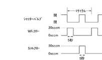
図1に示すように、成膜装置101は、真空チャンバー102と触媒室103とからなり、この真空チャンバー102と触媒室103とは、シャッターバルブ104のようなシャッター機構を介して仕切られており、真空チャンバー102には、バルブ、マスフローコントローラー(MFC)を備えた原料ガス導入配管105及び反応性ガス導入配管、並びに排気手段(図示せず)が接続されている。この原料ガス導入配管105の一端は、真空チャンバー102内に設けられたガス噴出手段106に接続され、原料ガスを真空チャンバー内に載置される成膜対象物であるウェハー107の表面に供給できるように構成されている。また、触媒室103には、反応性ガスを活性種に変換せしめることができる触媒体108が設置されている。この触媒室103にはまた、その室内を排気できるように直接に排気手段が設けられていてもよい。 As shown in FIG. 1, the
上記装置は次のようにして作動する。上記原料ガス、例えばWF6ガス、W(CO)6ガス等のような原料ガスを、シャッターバルブ104を閉じた状態で、原料ガス導入配管105を経て真空チャンバー102内へ導入し、ガス噴出手段106を介して、このガス噴出手段に対向して配置された成膜対象物であって、例えば予めSiO2膜やCu膜が形成されている所定の温度に加熱されたウェハー107の表面に供給し、表面上に原料ガスを吸着せしめる。このガス噴出手段106には、原料ガスをウェハー107の表面に均一に供給できるように、その中心方向にガス噴出用の穴が等間隔に設けられており、その形状は例えばリング状であることが好ましい。次いで、原料の導入を停止し、シャッターバルブ104を閉じた状態で所定の時間排気する。その後、シャッターバルブ104を開放すると同時に、SiH4、NH3、H2などの反応性ガスを少なくとも1種触媒室103内へ導入し、所定の温度に加熱されている触媒体108に接触させ、反応性の高いラジカルなどの中性物質に変換せしめ、生成したラジカルなどを真空チャンバー102内へ導入する。ウェハー107の表面に達したラジカルなどは、表面に吸着されていた原料と反応し、薄膜が形成される。The device operates as follows. A raw material gas such as WF6 gas, W (CO)6 gas or the like is introduced into the
次いで、反応性ガスの導入を停止すると同時に、シャッターバルブ104を閉じて、所定の時間排気する。このようなガスフローシーケンス、すなわち、原料ガスの吸着工程及び反応性ガスとの反応工程を所定の回数、例えば数回〜数十回繰り返し、所望の膜厚を有する薄膜を形成することができる。 Next, the introduction of the reactive gas is stopped, and at the same time, the
本発明で用いる上記触媒体は、ALD法で用いられるものであれば特に制限されず、例えば、W、Ta、Ti、Moなどの金属からなるワイヤー状、螺旋状などの触媒体であってもよく、通常真空雰囲気中で1500〜2000℃程度、好ましくは1700〜1800℃程度に加熱して用いられる。例えば、直径0.5mm程度の細線を用いる場合は、1本又は2本以上を平行に配置したり、網状に配置したりして用いる。 The catalyst body used in the present invention is not particularly limited as long as it is used in the ALD method. For example, it may be a wire or spiral catalyst body made of a metal such as W, Ta, Ti, or Mo. It is usually used by heating to about 1500 to 2000 ° C., preferably about 1700 to 1800 ° C. in a vacuum atmosphere. For example, when using a thin wire having a diameter of about 0.5 mm, one or two or more wires are arranged in parallel or arranged in a net shape.
上記原料ガスや反応性ガスを流す際には、アルゴンなどの不活性ガスを希釈ガス、キャリアーガスとして用いてもよい。また、各工程での排気時間は、吸着した原料ガス及び反応性ガス以外の剰余ガスを真空チャンバー内から除去するために行われる。さらに、反応性ガスと共に酸素含有ガス(O2ガスなど)などの添加ガスを流すと、得られた薄膜と成膜対象物との密着性はさらに向上する。原料ガスや反応性ガスを供給する際の到達圧力は特に制限はなく、例えば、10−2〜102Pa、好ましくは数Pa以下の範囲で、成膜目的に合わせて適宜設定すればよい。さらにまた、使用する反応性ガスは、少なくとも1種であり、2種類以上の反応性ガスを使用する場合には、触媒室内へ、それぞれ別々に所定の順番で、或いはそれぞれの混合ガスとして同時に導入しても良い。When flowing the source gas or the reactive gas, an inert gas such as argon may be used as a dilution gas or a carrier gas. Moreover, the exhaust time in each process is performed in order to remove surplus gases other than the adsorbed source gas and reactive gas from the vacuum chamber. Furthermore, when an additive gas such as an oxygen-containing gas (such as O2 gas) is flowed together with the reactive gas, the adhesion between the obtained thin film and the film formation target is further improved. The ultimate pressure at the time of supplying the raw material gas or the reactive gas is not particularly limited, and may be appropriately set according to the purpose of film formation, for example, in the range of 10−2 to 102 Pa, preferably several Pa or less. Furthermore, at least one type of reactive gas is used, and when two or more types of reactive gas are used, they are separately introduced into the catalyst chamber in a predetermined order or simultaneously as respective mixed gases. You may do it.
本発明の実施の形態の一つとして、原料ガスとしてWF6ガス、反応性ガスとしてSiH4、NH3ガスを用いてWxN膜を形成する場合について、図2に示すガスフローシーケンスに基づいて説明する。As one embodiment of the present invention, the case of forming a Wx N film using WF6 gas as a source gas and SiH4 or NH3 gas as a reactive gas is based on the gas flow sequence shown in FIG. I will explain.
まず、所定流量のWF6ガスを、シャッターバルブ104を閉じた状態で、ガス導入配管105を経て真空チャンバー102内へ所定の時間導入し、ガス噴出手段106から所定の温度に加熱されているウェハー107の表面に供給し、表面上に吸着せしめる。シャッターバルブ104を閉じた状態で、WF6ガスの導入を停止して真空チャンバー102内を所定の時間排気する。次いで、シャッターバルブ104を開放し、同時に、所定流量のSiH4ガスを所定の時間触媒室103内へ導入し、加熱されている触媒体108に接触させて反応性の高いラジカルに変換せしめ、生成したラジカルを真空チャンバー102内へ導入する。次いで、シャッターバルブ104を閉じ、同時に、SiH4ガスの導入を停止して真空チャンバー102内を所定の時間排気する。シャッターバルブ104を閉じた状態で、所定流量のWF6ガスを所定の時間真空チャンバー102内の加熱されているウェハー107表面に導入する。シャッターバルブ104を閉じた状態で、WF6ガスの導入を停止して真空チャンバー102内を排気する。次いで、シャッターバルブ104を開放し、同時に、所定流量のNH3ガスを所定の時間触媒室103へ導入し、加熱されている触媒体108に接触させて反応性の高いラジカルに変換せしめ、生成したラジカルを真空チャンバー102内へ導入する。その後、シャッターバルブ104を閉じ、同時に、NH3ガスの導入を停止して真空チャンバー102内を所定の時間排気する。これらのガスフローシーケンスを1サイクルとし、所定の回数繰り返すことによって、所望の膜厚を有するWxN膜を形成することができる。このようなガスフローシーケンスに従った成膜プロセスを、例えば10回程度繰り返すことにより膜厚5nm程度のWxN膜(xが5以上のWリッチな膜)を形成することができる。本発明では、W/N比が5以上、好ましくは5〜7、より好ましくは5〜6であれば、良好な比抵抗、バリア性を有する膜が得られる。First, a wafer having a predetermined flow rate of WF6 gas introduced into the
本発明によれば、原料ガスとしては、上記以外に、WCl6などのハロゲン化タングステンのガス、WOF2、WOF4、WOCl2、WOCl4などのオキシハロゲン化タングステンのガス、W(CO)5などのカルボニル化タングステンのガス、W(OC2H5)などの有機金属化合物のガスなどを用いることもできる。また、反応性ガスとしては、上記以外に、Si2H6などのジシランのガス、SiH2Cl2などのジハロゲン化シランのガス、ヒドラジン中のHがCxHyなどの炭化水素基で置換されたヒドラジン誘導体のガスなどを用いることもできる。In addition to the above, according to the present invention, other than the above, tungsten halide gas such as WCl6 , tungsten oxyhalide gas such as WOF2 , WOF4 , WOCl2 , WOCl4 , W (CO)5 A carbonylated tungsten gas such as W (OC2 H5 ) or an organic metal compound gas can also be used. In addition to the above, reactive gases include disilane gas such as Si2 H6 , dihalogenated silane gas such as SiH2 Cl2, and H in hydrazine is replaced with a hydrocarbon group such as Cx Hy. The gas of the hydrazine derivative made can also be used.
本実施例では、図1に示す成膜装置101を用い、原料ガスとしてWF6ガス及び反応性ガスとしてSiH4、NH3ガスを用い、図2のガスフローシーケンスに従ってWxN膜を形成した。In this example, the
シャッターバルブ104を閉じた状態で、ガス導入配管105を経て真空チャンバー102内へWF6ガスを20sccm、5秒間流し、ガス噴出手段106を介して250℃に加熱されている、予めSiO2膜やCu膜が形成されているウェハー107の表面に供給し、表面上に吸着せしめた。シャッターバルブ104を閉じた状態で、WF6ガスの導入を停止して真空チャンバー102内を5秒間排気した。シャッターバルブ104を開放し、同時に、SiH4ガスを50sccm、5秒間触媒室103内へ流し、1700℃に加熱されている触媒体108に接触させて反応性の高いラジカルに変換せしめ、生成したラジカルを真空チャンバー102内へ導入した。次いで、シャッターバルブ104を閉じ、同時に、SiH4ガスの導入を停止して真空チャンバー102内を5秒間排気した。シャッターバルブ104を閉じた状態で、WF6ガスを20sccm、5秒間、真空チャンバー102内の250℃に加熱されているウェハー107表面に流した。シャッターバルブ104を閉じた状態で、WF6ガスの導入を停止して真空チャンバー102内を5秒間排気した。次いで、シャッターバルブ104を開放し、同時に、NH3ガスを50sccm、5秒間、触媒室103へ流し、1700℃に加熱されている触媒体108に接触させて反応性の高いラジカルに変換せしめ、生成したラジカルを真空チャンバー102内へ導入した。その後、シャッターバルブ104を閉じ、同時に、NH3ガスの導入を停止して真空チャンバー102内を5秒間排気した。これらのガスフローシーケンスを1サイクルとし、10サイクル及び20サイクル繰り返して、それぞれ、5nm及び10nm程度の膜厚を有するWxN膜(いずれの膜の場合も、xは5以上のWリッチな膜であった)を形成することができた。この膜のうち、20サイクル繰り返した場合に得られた膜は、xがほぼ5.3のWxN膜であった。In the closed state of the
比較のために、触媒体を用いない従来のALD法により、原料ガスとしてWF6ガス及び反応性ガスとしてSiH4、NH3ガスを用い、上記に準じてWxN膜を形成した。For comparison, a Wx N film was formed according to the above by using a conventional ALD method without a catalyst body, using WF6 gas as a source gas and SiH4 and NH3 gas as a reactive gas.
すなわち、真空チャンバー内へWF6ガスを20sccm、5秒間流し、ガス噴出手段106を介して、NH3プラズマで前処理された、270℃に加熱されているウェハー107の表面に供給し、表面上に吸着せしめた。次いで、SiH4ガスを50sccm、5秒間、真空チャンバー102内へ導入した。その後、WF6ガスを20sccm、5秒間、真空チャンバー内の270℃に加熱されているウェハー表面に流した。その後、NH3ガスを50sccm、5秒間、真空チャンバー内へ導入した。これらのガスフローシーケンスを1サイクルとし、20サイクル繰り返して、10nmの膜厚を有するWxN膜を形成した。この場合、xはほぼ2.8であった。That is, WF6 gas was allowed to flow into the vacuum chamber at 20 sccm for 5 seconds, and was supplied to the surface of the
上記のようにして触媒体を用いるALD法(以下、CAT−ALD法と呼ぶ)により形成したWxN膜と従来のALD法により形成したWxN膜との特性を比較した。その結果を表1に示す。ALD method using a catalytic element as described above (hereinafter, referred to as CAT-ALD method) comparison of characteristics of theW x N film formed byW x N film and the conventional ALD method formed by. The results are shown in Table 1.
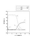
表1において、比抵抗ρ(μΩcm)は、4探針プローブ法でシート抵抗(Rs)を測定し、SEMで膜厚(T)を測定して、式:ρ=Rs・Tに基づいて算出したものである。また、密着性は、8インチウェハー上のSiO2膜の表面やPVD法により堆積させたCu膜(膜厚200nm)の表面にバリアメタル膜(WxN膜)10nmを堆積させた後、公知のテープテストにより得られた肉眼観察結果である。さらに、表1中の不純物(Si、F)濃度は、上記のようにして形成した2種類のWxN膜に対し、オージェ電子分光法(AES)により組成分析を行った結果であり、そのスペクトルを図3及び4に示す。In Table 1, the specific resistance ρ (μΩcm) is calculated based on the formula: ρ = Rs · T by measuring the sheet resistance (Rs) by the 4-probe probe method and measuring the film thickness (T) by SEM. It is a thing. The adhesion is known after depositing a 10 nm barrier metal film (Wx N film) on the surface of a SiO2 film on an 8-inch wafer or the surface of a Cu film (thickness 200 nm) deposited by the PVD method. It is the result of visual observation obtained by the tape test. Furthermore, the impurity (Si, F) concentration in Table 1 is a result of composition analysis by Auger electron spectroscopy (AES) on the two types of Wx N films formed as described above. The spectra are shown in FIGS.
表1から明らかなように、本発明のCAT−ALD法によれば、酸化膜(SiO2膜)表面を予めNH3プラズマに曝しておかなくとも、230℃という低温で220μΩcmという低抵抗WxN膜を得ることができた。SiO2膜及びCu膜への密着性に関しては、CAT−ALD法の場合も、従来のALD法の場合もウェハー全面において膜剥離は見られず、バリアメタル膜は酸化物膜及びCu膜に対して強固な密着性を示した。As is apparent from Table 1, according to the CAT-ALD method of the present invention, the low resistance Wx of 220 μΩcm at a low temperature of 230 ° C. is obtained even if the surface of the oxide film (SiO2 film) is not exposed to NH3 plasma in advance. An N film could be obtained. Regarding the adhesion to the SiO2 film and the Cu film, neither the CAT-ALD method nor the conventional ALD method showed film peeling on the entire surface of the wafer, and the barrier metal film was compared with the oxide film and the Cu film. And showed strong adhesion.
また、図3に示すAESによる分析結果によれば、CAT−ALD法の場合、膜中のSi及びFの濃度に関しては、Si濃度は0.9%であり、F濃度は0.18%であった。また、Wはほぼ80%であり、Nは15%であるので、xはほぼ5.3であった。図4に示すAESによる分析結果によれば、従来のALD法の場合、CAT−ALD法の場合に比べて、Si濃度は6.7%と極めて高く、また、F濃度も0.6%と高かった。この場合、Wはほぼ70%であり、Nはほぼ15%であるので、xはほぼ2.8であった。図3及び4において、線a、b、c、d、e及びfは、それぞれ膜中の元素W、N、Si、F、O及びCに対するスパッタエッチ時間(秒)と原子濃度(%)との関係を示すオージェ電子のスペクトルである。 Further, according to the analysis result by AES shown in FIG. 3, in the case of the CAT-ALD method, regarding the Si and F concentrations in the film, the Si concentration is 0.9% and the F concentration is 0.18%. there were. Further, since W is approximately 80% and N is 15%, x is approximately 5.3. According to the analysis result by AES shown in FIG. 4, in the case of the conventional ALD method, the Si concentration is very high as 6.7% and the F concentration is also 0.6% as compared with the case of the CAT-ALD method. it was high. In this case, W was approximately 70% and N was approximately 15%, so x was approximately 2.8. 3 and 4, lines a, b, c, d, e, and f represent the sputter etch time (seconds) and atomic concentration (%) for the elements W, N, Si, F, O, and C in the film, respectively. It is a spectrum of Auger electrons showing the relationship.
ところで、膜中に含まれる不純物のうち、Siは酸化物膜に対する密着性を低下させる原因となるし、FはCuと反応してCuFを形成するので、配線の信頼性を低下させてしまうという問題がある。しかるに、上記したように、図3及び4によれば、CAT−ALD法によりWxN膜を形成した場合、触媒を使わないALD法の場合に比べてSi、F含量が少ないので、本発明に従って形成されたWxN膜は、酸化物膜に対する密着性が優れ、かつCu配線の信頼性を損なうこともないことが分かる。なお、上記したように、CAT−ALD法により形成されたWxN膜中のSi、F濃度が低いのは、反応性の高いSiH4のラジカル、NH3のラジカル、WF6との間の反応は、化学量論的な理想に近い形(上記反応式(1)及び(3))で起こるために、不純物が入りにくいものと考えられる。By the way, among impurities contained in the film, Si causes a decrease in adhesion to the oxide film, and F reacts with Cu to form CuF, thereby reducing the reliability of the wiring. There's a problem. However, as described above, according to FIGS. 3 and 4, when the Wx N film is formed by the CAT-ALD method, the Si and F contents are less than those in the case of the ALD method without using the catalyst. It can be seen that the Wx N film formed according to the above has excellent adhesion to the oxide film and does not impair the reliability of the Cu wiring. As described above, the Si and F concentrations in the Wx N film formed by the CAT-ALD method are low because of the high reactivity between SiH4 radicals, NH3 radicals, and WF6 . Since the reaction occurs in a form close to the stoichiometric ideal (the above reaction formulas (1) and (3)), it is considered that impurities are difficult to enter.
(比較例1)
実施例1において用いた反応性ガスであるNH3ガス及びSiH4ガスの流す順序を変え、最初にNH3ガスを流し、次いでSiH4ガスを流して同様にしてWxN成膜プロセスを実施した。得られたWxN膜中のwの比率は5以下であり、膜全体に占めるwの比率が1.5程度であるWxNが酸化物膜表面上に10%程度存在し、得られた膜の比抵抗は数千から数万μΩcmと高く、また、下地膜との密着性を劣化させた。(Comparative Example 1)
The flow sequence of the NH3 gas and SiH4 gas, which are the reactive gases used in Example 1, was changed, the NH3 gas was first flowed, and then the SiH4 gas was flowed to carry out the Wx N film forming process in the same manner. did. The ratio of w in the obtained Wx N film is 5 or less, and about 10% of Wx N having a ratio of w to the entire film of about 1.5 is present on the surface of the oxide film. The specific resistance of the film was as high as several thousand to several tens of thousands of μΩcm, and the adhesion with the base film was deteriorated.
本実施例では、図1に示す成膜装置101を用い、実施例1に準じて、但し原料ガスとしてWF6ガス及び反応性ガスとしてSiH4ガスを用い、また、図5のガスフローシーケンスに従ってW膜を形成した。In this example, the
シャッターバルブ104を閉じた状態で、ガス導入配管105を経て真空チャンバー102内へWF6ガスを20sccm、5秒間流し、ガス噴出手段106を介して250℃に加熱されているウェハー107の表面に供給し、表面上に吸着せしめた。シャッターバルブ104を閉じた状態で、WF6ガスの導入を停止して真空チャンバー内を5秒間排気した。その後、シャッターバルブ104を開放し、同時に、SiH4ガスを50sccm、5秒間触媒室103内へ流し、1700℃に加熱されている触媒体108に接触させ、反応性の高いラジカルに変換せしめ、生成したラジカルを真空チャンバー102内へ導入した。その後、シャッターバルブ104を閉じて5秒間排気した。これらのガスフローシーケンスを1サイクルとし、40サイクル繰り返して、15nmの膜厚を有するW膜を形成することができた。With the
比較のために、触媒体を用いない従来のALD法により、原料ガスとしてWF6ガス及び反応性ガスとしてSiH4ガスを用い、上記に準じてW膜を形成した。For comparison, a W film was formed in accordance with the above by using a conventional ALD method without using a catalyst body, using WF6 gas as a source gas and SiH4 gas as a reactive gas.
すなわち、真空チャンバー102内へWF6ガスを20sccm、5秒間流し、ガス噴出手段106を介して、270℃に加熱されているウェハー107の表面に供給し、表面上に吸着せしめた。次いで、真空チャンバー102を5秒間排気した後、SiH4ガスを50sccm、5秒間、真空チャンバー102内へ導入した。その後、真空チャンバー102内を5秒間排気した。これらのガスフローシーケンスを1サイクルとし、40サイクル繰り返して、20nmの膜厚を有するW膜を形成した。That is, WF6 gas was allowed to flow into the
上記のようにしてCAT−ALD法により形成したW膜と従来のALD法に従って形成したW膜とについて、オージェ電子分光法(AES)により組成分析を行い、不純物濃度を調べた。得られたスペクトルをそれぞれ図6及び7に示す。 The W film formed by the CAT-ALD method as described above and the W film formed by the conventional ALD method were subjected to composition analysis by Auger electron spectroscopy (AES), and the impurity concentration was examined. The obtained spectra are shown in FIGS. 6 and 7, respectively.
図6に示すAESによる分析結果によれば、CAT−ALD法の場合、膜中のSi濃度に関しては、0.5%と極めて低く、また、図7に示すAESによる分析結果によれば、従来のALD法の場合、膜中のSi濃度に関しては、CAT−ALD法の場合に比べて、37%と極めて高かった。図6及び7において、線a、b、c、d、e及びfは、それぞれ膜中の元素W、N、Si、F、O及びCに対するスパッタエッチ時間(秒)と原子濃度(%)との関係を示すオージェ電子のスペクトルである。 According to the analysis result by AES shown in FIG. 6, in the case of the CAT-ALD method, the Si concentration in the film is extremely low as 0.5%, and according to the analysis result by AES shown in FIG. In the case of the ALD method, the Si concentration in the film was extremely high at 37% compared to the case of the CAT-ALD method. 6 and 7, lines a, b, c, d, e, and f represent the sputter etch time (seconds) and atomic concentration (%) for the elements W, N, Si, F, O, and C in the film, respectively. It is a spectrum of Auger electrons showing the relationship.
ところで、図6及び7によれば、CAT−ALD法によりW膜を形成した場合、触媒を使わないALD法の場合に比べて圧倒的にSi含量が少ないのは、ほぼ純粋なW膜が得られているといえ、触媒を使わないALD法の場合は、WSix膜が形成されてしまう。このように、CAT−ALD法により形成したW膜中のSi濃度が低いのは、反応性の高いSiH4のラジカルとWF6との反応は、化学量論的な理想に近い形(上記反応式(1))で起こるためであると考えられる。一方、触媒を使わないALD法の場合は、上記反応式(2)に従って反応が起こるためであると考えられる。By the way, according to FIGS. 6 and 7, when the W film is formed by the CAT-ALD method, the Si content is overwhelmingly smaller than that in the case of the ALD method without using a catalyst. However, in the case of the ALD method that does not use a catalyst, a WSix film is formed. Thus, the Si concentration in the W film formed by the CAT-ALD method is low because the reaction between the highly reactive SiH4 radical and WF6 is close to the stoichiometric ideal (the above reaction). This is considered to be caused by the equation (1)). On the other hand, in the case of the ALD method without using a catalyst, it is considered that the reaction occurs according to the above reaction formula (2).
上記したように、CAT−ALD法によりW膜を形成した場合、触媒を使わないALD法の場合に比べてSi含量が少ないので、本発明に従って形成されたW膜は、酸化物膜に対する密着性が優れ、また、F含量も極めて少ないので、Cu配線の信頼性を損なうこともないことが分かる。 As described above, when the W film is formed by the CAT-ALD method, the Si content is smaller than that in the case of the ALD method without using a catalyst. Therefore, the W film formed according to the present invention has an adhesion property to the oxide film. In addition, since the F content is extremely small, it is understood that the reliability of the Cu wiring is not impaired.
本実施例では、図1に示す成膜装置101により、原料ガスとしてWF6ガス及び反応性ガスとしてSiH4、NH3ガスを用いてWxN膜を形成した。In this example, a Wx N film was formed by using the
まず、1.4Paに設定された触媒室103内にH2ガス200sccmを流して、1700℃に加熱されている触媒体に接触させ、生成したラジカルを真空チャンバー102へ導入して成膜対象物であるウェハー107表面の前処理を行い、そのホールやトレンチの底面に露出しているCu膜などの金属膜表面の酸化物を還元除去せしめ、清浄な金属表面を露出せしめた。なお、H2以外の反応性ガスを用いても同様な結果が得られる。First, 200 sccm of H2 gas is caused to flow through the
上記前処理後、シャッターバルブ104を閉じた状態で、ガス導入配管105を経て真空チャンバー102内へWF6ガスを20sccm、10秒間流し、ガス噴出手段106を介して250℃に加熱されている予めSiO2膜やCu膜が形成されているウェハー107の表面に供給し、表面上に吸着せしめた。シャッターバルブ104を閉じた状態で、WF6ガスの導入を停止して真空チャンバー102を10秒間排気した。次いで、シャッターバルブ104を開放し、同時に、SiH4ガスを50sccm、10秒間触媒室103内へ流し、1700℃に加熱されている触媒体108に接触させて反応性の高いラジカルに変換せしめ、生成したラジカルを真空チャンバー102内へ導入した。次いで、シャッターバルブ104を閉じ、同時に、SiH4ガスの導入を停止して真空チャンバー102内を10秒間排気した。シャッターバルブ104を閉じた状態で、WF6ガスを20sccm、10秒間、真空チャンバー102内の250℃に加熱されているウェハー107表面に流した。シャッターバルブ104を閉じた状態で、WF6ガスの導入を停止して真空チャンバー102内を10秒間排気した。次いで、シャッターバルブ104を開放して、同時に、NH3ガスを50sccm、10秒間、触媒室103へ流し、1700℃に加熱されている触媒体108に接触させて反応性の高いラジカル変換せしめ、生成したラジカルを真空チャンバー102内へ導入した。その後、シャッターバルブ104を閉じ、同時に、NH3ガスの導入を停止して真空チャンバー102内を10秒間排気した。これらのガスフローシーケンスを1サイクルとし、20サイクル繰り返して、11nmの膜厚を有し、比抵抗290μΩcmのWxN膜(xが5以上のWリッチな膜であった)を形成することができた。この膜は、密着性に優れ、Cu配線の信頼性を損なうこともなかった。After the above pre-treatment, with the
また、上記と同様なガスフローシーケンスを60サイクル繰り返したところ、33nmの膜厚を有し、比抵抗250μΩcmのWxN膜を形成することができた。Further, when the same gas flow sequence as described above was repeated 60 cycles, a Wx N film having a thickness of 33 nm and a specific resistance of 250 μΩcm could be formed.
実施例2記載の方法に準じて、但し原料ガスとしてWF6ガス及び反応性ガスとしてSiH4ガスを用いてW又はWSix膜を形成した。In accordance with the method described in Example 2, a W or WSix film was formed using WF6 gas as a source gas and SiH4 gas as a reactive gas.
すなわち、シャッターバルブ104を閉じた状態で、ガス導入配管105を経て真空チャンバー102内へWF6ガスを20sccm、10秒間流し、ガス噴出手段106を介して250℃に加熱されているウェハー107の表面に供給し、表面上に吸着せしめた。次いで、シャッターバルブ104を閉じた状態で10秒間排気した後に、シャッターバルブ104を開放して、SiH4ガスを50sccm、10秒間触媒室103内へ流し、1700℃に加熱されている触媒体108に接触させ、反応性の高いラジカルに変換せしめ、生成したラジカルを真空チャンバー102内へ導入した。その後、10秒間排気した。これらのガスフローシーケンスを1サイクルとし、40サイクル繰り返して15nmの膜厚を有するW膜を形成せしめた。得られた膜の比抵抗は80μΩcmであった。That is, with the
実施例1記載の方法に準じて、但し原料ガスとしてWF6ガス及び反応性ガスとしてNH3ガスとSiH4ガスとの混合ガスを用いて低抵抗のWxN膜を形成した。In accordance with the method described in Example 1, a low resistance Wx N film was formed using WF6 gas as a raw material gas and a mixed gas of NH3 gas and SiH4 gas as a reactive gas.
すなわち、シャッターバルブ104を閉じた状態で、ガス導入配管105を経て真空チャンバー102内へWF6ガスを20sccm、10秒間流し、ガス噴出手段106を介して250℃に加熱されており、予めSiO2膜やCu膜の形成されていたウェハー107の表面に供給し、表面上に吸着せしめた。10秒間排気した後に、NH3ガスとSiH4ガスとの等量混合ガスを50sccm、10秒間触媒室103内へ流し、1700℃に加熱されている触媒体108に接触させ、反応性の高いラジカルに変換せしめた。次いで、シャッターバルブ104を開放し、生成したラジカルを真空チャンバー102内へ導入した。その後、10秒間排気した。これらのガスフローシーケンスを1サイクルとし、20サイクル繰り返して10nmの膜厚を有するWxN膜を形成せしめた。得られた膜の比抵抗は実施例1の場合と同程度であった。この膜は、密着性に優れ、Cu配線の信頼性を損なうこともなかった。That is, with the
実施例1記載の方法に準じて、但し原料ガスとしてWF6ガス及び反応性ガスとしてNH3ガスとH2ガスとの混合ガスを用いて低抵抗WxN膜を形成した。In accordance with the method described in Example 1, a low-resistance Wx N film was formed using WF6 gas as a source gas and a mixed gas of NH3 gas and H2 gas as a reactive gas.
すなわち、シャッターバルブ104を閉じた状態で、ガス導入配管105を経て真空チャンバー102内へWF6ガスを20sccm、10秒間流し、ガス噴出手段106を介して250℃に加熱されており、予めSiO2膜やCu膜の形成されていたウェハー107の表面に供給し、表面上に吸着せしめた。10秒間排気した後に、NH3ガスとH2ガスとの等量混合ガスを50sccm、10秒間触媒室103内へ流し、1700℃に加熱されている触媒体108に接触させ、反応性の高いラジカルに変換せしめた。次いで、シャッターバルブ104を開放し、生成したラジカルを真空チャンバー102内へ導入した。その後、10秒間排気した。これらのガスフローシーケンスを1サイクルとし、20サイクル繰り返して10nmの膜厚を有するWxN膜を形成せしめた。得られた膜の比抵抗は実施例1の場合と同程度であった。この膜は、密着性に優れ、Cu配線の信頼性を損なうこともなかった。That is, with the
なお、反応性ガスとしてNH3ガス及びH2ガスを混合ガスではなく、別々に用いた場合には、原料ガスの後に、最初にH2ガスを流し、その後NH3ガスを流す方が最初にNH3ガスを流し、その後H2ガスを流すよりも膜中のwの比率は高く、得られた膜の比抵抗も低い。In addition, when NH3 gas and H2 gas are used separately as a reactive gas instead of a mixed gas, it is first to flow H2 gas first after the source gas and then flow NH3 gas first. The ratio of w in the film is higher than that of flowing NH3 gas and then H2 gas, and the specific resistance of the obtained film is also low.
本発明の薄膜形成方法によれば、事前にNH3プラズマ処理により表面改質を行うことなく、低温(例えば、ウェハー温度230℃以下)において、膜の比抵抗が低く(好ましくは、300μΩcm以下)、かつ下層の酸化膜及びCu膜などに対して密着性に優れ、Cu配線の信頼性を損なうことのないバリアメタル膜を形成することができる。そのため、本発明は、例えば、ホール、トレンチ等の内部をCuやAl等の配線材料で埋め込んで半導体集積回路を作製する技術分野に適用できる。According to the thin film forming method of the present invention, the specific resistance of the film is low (preferably, 300 μΩcm or less) at a low temperature (for example, a wafer temperature of 230 ° C. or less) without surface modification by NH3 plasma treatment in advance. In addition, it is possible to form a barrier metal film that has excellent adhesion to the underlying oxide film, Cu film, and the like and does not impair the reliability of the Cu wiring. Therefore, the present invention can be applied to a technical field in which a semiconductor integrated circuit is manufactured by embedding holes, trenches, and the like with a wiring material such as Cu or Al.
101 成膜装置 102 真空チャンバー
103 触媒室 104 シャッターバルブ
105 原料ガス導入配管 106 ガス噴出手段
107 ウェハー 108 触媒体DESCRIPTION OF
Claims (10)
Translated fromJapanesePriority Applications (1)
| Application Number | Priority Date | Filing Date | Title |
|---|---|---|---|
| JP2004207752AJP4674061B2 (en) | 2004-07-14 | 2004-07-14 | Thin film formation method |
Applications Claiming Priority (1)
| Application Number | Priority Date | Filing Date | Title |
|---|---|---|---|
| JP2004207752AJP4674061B2 (en) | 2004-07-14 | 2004-07-14 | Thin film formation method |
Publications (2)
| Publication Number | Publication Date |
|---|---|
| JP2006028572A JP2006028572A (en) | 2006-02-02 |
| JP4674061B2true JP4674061B2 (en) | 2011-04-20 |
Family
ID=35895280
Family Applications (1)
| Application Number | Title | Priority Date | Filing Date |
|---|---|---|---|
| JP2004207752AExpired - LifetimeJP4674061B2 (en) | 2004-07-14 | 2004-07-14 | Thin film formation method |
Country Status (1)
| Country | Link |
|---|---|
| JP (1) | JP4674061B2 (en) |
Families Citing this family (283)
| Publication number | Priority date | Publication date | Assignee | Title |
|---|---|---|---|---|
| EP2039799A4 (en)* | 2006-04-18 | 2015-09-30 | Ulvac Inc | Film forming apparatus and barrier film manufacturing method |
| JP5135710B2 (en)* | 2006-05-16 | 2013-02-06 | 東京エレクトロン株式会社 | Film forming method and film forming apparatus |
| JP2008034684A (en)* | 2006-07-31 | 2008-02-14 | Sony Corp | Solid-state imaging device, manufacturing method thereof, and imaging apparatus |
| WO2008143024A1 (en)* | 2007-05-23 | 2008-11-27 | Canon Anelva Corporation | Thin film forming apparatus |
| WO2012049823A1 (en)* | 2010-10-15 | 2012-04-19 | 株式会社アルバック | Semiconductor device production method and semiconductor device |
| US20130023129A1 (en) | 2011-07-20 | 2013-01-24 | Asm America, Inc. | Pressure transmitter for a semiconductor processing environment |
| US8952355B2 (en) | 2011-09-29 | 2015-02-10 | Intel Corporation | Electropositive metal containing layers for semiconductor applications |
| US10714315B2 (en) | 2012-10-12 | 2020-07-14 | Asm Ip Holdings B.V. | Semiconductor reaction chamber showerhead |
| US20160376700A1 (en) | 2013-02-01 | 2016-12-29 | Asm Ip Holding B.V. | System for treatment of deposition reactor |
| JP6554418B2 (en) | 2013-11-27 | 2019-07-31 | 東京エレクトロン株式会社 | Tungsten film forming method and film forming apparatus |
| US11015245B2 (en) | 2014-03-19 | 2021-05-25 | Asm Ip Holding B.V. | Gas-phase reactor and system having exhaust plenum and components thereof |
| JP6608026B2 (en)* | 2014-03-25 | 2019-11-20 | 東京エレクトロン株式会社 | Method and apparatus for forming tungsten film |
| US10941490B2 (en) | 2014-10-07 | 2021-03-09 | Asm Ip Holding B.V. | Multiple temperature range susceptor, assembly, reactor and system including the susceptor, and methods of using the same |
| JP6706903B2 (en) | 2015-01-30 | 2020-06-10 | 東京エレクトロン株式会社 | Method for forming tungsten film |
| CN105839068B (en) | 2015-01-30 | 2018-09-21 | 东京毅力科创株式会社 | The film build method of tungsten film |
| US10276355B2 (en) | 2015-03-12 | 2019-04-30 | Asm Ip Holding B.V. | Multi-zone reactor, system including the reactor, and method of using the same |
| JP6416679B2 (en) | 2015-03-27 | 2018-10-31 | 東京エレクトロン株式会社 | Method for forming tungsten film |
| JP6541438B2 (en) | 2015-05-28 | 2019-07-10 | 東京エレクトロン株式会社 | Method of reducing stress of metal film and method of forming metal film |
| JP6478813B2 (en) | 2015-05-28 | 2019-03-06 | 東京エレクトロン株式会社 | Method for forming metal film |
| US10458018B2 (en) | 2015-06-26 | 2019-10-29 | Asm Ip Holding B.V. | Structures including metal carbide material, devices including the structures, and methods of forming same |
| US11139308B2 (en) | 2015-12-29 | 2021-10-05 | Asm Ip Holding B.V. | Atomic layer deposition of III-V compounds to form V-NAND devices |
| US10529554B2 (en) | 2016-02-19 | 2020-01-07 | Asm Ip Holding B.V. | Method for forming silicon nitride film selectively on sidewalls or flat surfaces of trenches |
| US10343920B2 (en) | 2016-03-18 | 2019-07-09 | Asm Ip Holding B.V. | Aligned carbon nanotubes |
| JP6710089B2 (en) | 2016-04-04 | 2020-06-17 | 東京エレクトロン株式会社 | Method for forming tungsten film |
| US10367080B2 (en) | 2016-05-02 | 2019-07-30 | Asm Ip Holding B.V. | Method of forming a germanium oxynitride film |
| US11453943B2 (en) | 2016-05-25 | 2022-09-27 | Asm Ip Holding B.V. | Method for forming carbon-containing silicon/metal oxide or nitride film by ALD using silicon precursor and hydrocarbon precursor |
| US10612137B2 (en) | 2016-07-08 | 2020-04-07 | Asm Ip Holdings B.V. | Organic reactants for atomic layer deposition |
| US9859151B1 (en) | 2016-07-08 | 2018-01-02 | Asm Ip Holding B.V. | Selective film deposition method to form air gaps |
| US10714385B2 (en)* | 2016-07-19 | 2020-07-14 | Asm Ip Holding B.V. | Selective deposition of tungsten |
| US9812320B1 (en) | 2016-07-28 | 2017-11-07 | Asm Ip Holding B.V. | Method and apparatus for filling a gap |
| KR102532607B1 (en) | 2016-07-28 | 2023-05-15 | 에이에스엠 아이피 홀딩 비.브이. | Substrate processing apparatus and method of operating the same |
| US9887082B1 (en) | 2016-07-28 | 2018-02-06 | Asm Ip Holding B.V. | Method and apparatus for filling a gap |
| US11532757B2 (en) | 2016-10-27 | 2022-12-20 | Asm Ip Holding B.V. | Deposition of charge trapping layers |
| US10714350B2 (en) | 2016-11-01 | 2020-07-14 | ASM IP Holdings, B.V. | Methods for forming a transition metal niobium nitride film on a substrate by atomic layer deposition and related semiconductor device structures |
| KR102546317B1 (en) | 2016-11-15 | 2023-06-21 | 에이에스엠 아이피 홀딩 비.브이. | Gas supply unit and substrate processing apparatus including the same |
| KR102762543B1 (en) | 2016-12-14 | 2025-02-05 | 에이에스엠 아이피 홀딩 비.브이. | Substrate processing apparatus |
| US11447861B2 (en) | 2016-12-15 | 2022-09-20 | Asm Ip Holding B.V. | Sequential infiltration synthesis apparatus and a method of forming a patterned structure |
| US11581186B2 (en) | 2016-12-15 | 2023-02-14 | Asm Ip Holding B.V. | Sequential infiltration synthesis apparatus |
| KR102700194B1 (en) | 2016-12-19 | 2024-08-28 | 에이에스엠 아이피 홀딩 비.브이. | Substrate processing apparatus |
| US10269558B2 (en) | 2016-12-22 | 2019-04-23 | Asm Ip Holding B.V. | Method of forming a structure on a substrate |
| US11390950B2 (en) | 2017-01-10 | 2022-07-19 | Asm Ip Holding B.V. | Reactor system and method to reduce residue buildup during a film deposition process |
| US10468261B2 (en) | 2017-02-15 | 2019-11-05 | Asm Ip Holding B.V. | Methods for forming a metallic film on a substrate by cyclical deposition and related semiconductor device structures |
| US10529563B2 (en) | 2017-03-29 | 2020-01-07 | Asm Ip Holdings B.V. | Method for forming doped metal oxide films on a substrate by cyclical deposition and related semiconductor device structures |
| US10770286B2 (en) | 2017-05-08 | 2020-09-08 | Asm Ip Holdings B.V. | Methods for selectively forming a silicon nitride film on a substrate and related semiconductor device structures |
| US12040200B2 (en) | 2017-06-20 | 2024-07-16 | Asm Ip Holding B.V. | Semiconductor processing apparatus and methods for calibrating a semiconductor processing apparatus |
| US11306395B2 (en) | 2017-06-28 | 2022-04-19 | Asm Ip Holding B.V. | Methods for depositing a transition metal nitride film on a substrate by atomic layer deposition and related deposition apparatus |
| KR20190009245A (en) | 2017-07-18 | 2019-01-28 | 에이에스엠 아이피 홀딩 비.브이. | Methods for forming a semiconductor device structure and related semiconductor device structures |
| US10541333B2 (en) | 2017-07-19 | 2020-01-21 | Asm Ip Holding B.V. | Method for depositing a group IV semiconductor and related semiconductor device structures |
| US11018002B2 (en) | 2017-07-19 | 2021-05-25 | Asm Ip Holding B.V. | Method for selectively depositing a Group IV semiconductor and related semiconductor device structures |
| US11374112B2 (en) | 2017-07-19 | 2022-06-28 | Asm Ip Holding B.V. | Method for depositing a group IV semiconductor and related semiconductor device structures |
| US10590535B2 (en) | 2017-07-26 | 2020-03-17 | Asm Ip Holdings B.V. | Chemical treatment, deposition and/or infiltration apparatus and method for using the same |
| US10692741B2 (en) | 2017-08-08 | 2020-06-23 | Asm Ip Holdings B.V. | Radiation shield |
| US10770336B2 (en) | 2017-08-08 | 2020-09-08 | Asm Ip Holding B.V. | Substrate lift mechanism and reactor including same |
| US11139191B2 (en) | 2017-08-09 | 2021-10-05 | Asm Ip Holding B.V. | Storage apparatus for storing cassettes for substrates and processing apparatus equipped therewith |
| US11769682B2 (en) | 2017-08-09 | 2023-09-26 | Asm Ip Holding B.V. | Storage apparatus for storing cassettes for substrates and processing apparatus equipped therewith |
| US11830730B2 (en) | 2017-08-29 | 2023-11-28 | Asm Ip Holding B.V. | Layer forming method and apparatus |
| US11056344B2 (en) | 2017-08-30 | 2021-07-06 | Asm Ip Holding B.V. | Layer forming method |
| US11295980B2 (en) | 2017-08-30 | 2022-04-05 | Asm Ip Holding B.V. | Methods for depositing a molybdenum metal film over a dielectric surface of a substrate by a cyclical deposition process and related semiconductor device structures |
| KR102491945B1 (en) | 2017-08-30 | 2023-01-26 | 에이에스엠 아이피 홀딩 비.브이. | Substrate processing apparatus |
| US10658205B2 (en) | 2017-09-28 | 2020-05-19 | Asm Ip Holdings B.V. | Chemical dispensing apparatus and methods for dispensing a chemical to a reaction chamber |
| US10403504B2 (en) | 2017-10-05 | 2019-09-03 | Asm Ip Holding B.V. | Method for selectively depositing a metallic film on a substrate |
| US10923344B2 (en) | 2017-10-30 | 2021-02-16 | Asm Ip Holding B.V. | Methods for forming a semiconductor structure and related semiconductor structures |
| US11022879B2 (en) | 2017-11-24 | 2021-06-01 | Asm Ip Holding B.V. | Method of forming an enhanced unexposed photoresist layer |
| WO2019103613A1 (en) | 2017-11-27 | 2019-05-31 | Asm Ip Holding B.V. | A storage device for storing wafer cassettes for use with a batch furnace |
| CN111344522B (en) | 2017-11-27 | 2022-04-12 | 阿斯莫Ip控股公司 | Including clean mini-environment device |
| US10872771B2 (en) | 2018-01-16 | 2020-12-22 | Asm Ip Holding B. V. | Method for depositing a material film on a substrate within a reaction chamber by a cyclical deposition process and related device structures |
| TWI799494B (en) | 2018-01-19 | 2023-04-21 | 荷蘭商Asm 智慧財產控股公司 | Deposition method |
| KR102695659B1 (en) | 2018-01-19 | 2024-08-14 | 에이에스엠 아이피 홀딩 비.브이. | Method for depositing a gap filling layer by plasma assisted deposition |
| US11081345B2 (en) | 2018-02-06 | 2021-08-03 | Asm Ip Holding B.V. | Method of post-deposition treatment for silicon oxide film |
| WO2019158960A1 (en) | 2018-02-14 | 2019-08-22 | Asm Ip Holding B.V. | A method for depositing a ruthenium-containing film on a substrate by a cyclical deposition process |
| US10896820B2 (en) | 2018-02-14 | 2021-01-19 | Asm Ip Holding B.V. | Method for depositing a ruthenium-containing film on a substrate by a cyclical deposition process |
| US10731249B2 (en) | 2018-02-15 | 2020-08-04 | Asm Ip Holding B.V. | Method of forming a transition metal containing film on a substrate by a cyclical deposition process, a method for supplying a transition metal halide compound to a reaction chamber, and related vapor deposition apparatus |
| KR102636427B1 (en) | 2018-02-20 | 2024-02-13 | 에이에스엠 아이피 홀딩 비.브이. | Substrate processing method and apparatus |
| US10975470B2 (en) | 2018-02-23 | 2021-04-13 | Asm Ip Holding B.V. | Apparatus for detecting or monitoring for a chemical precursor in a high temperature environment |
| US11473195B2 (en) | 2018-03-01 | 2022-10-18 | Asm Ip Holding B.V. | Semiconductor processing apparatus and a method for processing a substrate |
| US11629406B2 (en) | 2018-03-09 | 2023-04-18 | Asm Ip Holding B.V. | Semiconductor processing apparatus comprising one or more pyrometers for measuring a temperature of a substrate during transfer of the substrate |
| US11114283B2 (en) | 2018-03-16 | 2021-09-07 | Asm Ip Holding B.V. | Reactor, system including the reactor, and methods of manufacturing and using same |
| KR102646467B1 (en) | 2018-03-27 | 2024-03-11 | 에이에스엠 아이피 홀딩 비.브이. | Method of forming an electrode on a substrate and a semiconductor device structure including an electrode |
| US11230766B2 (en) | 2018-03-29 | 2022-01-25 | Asm Ip Holding B.V. | Substrate processing apparatus and method |
| US11088002B2 (en) | 2018-03-29 | 2021-08-10 | Asm Ip Holding B.V. | Substrate rack and a substrate processing system and method |
| KR102600229B1 (en) | 2018-04-09 | 2023-11-10 | 에이에스엠 아이피 홀딩 비.브이. | Substrate supporting device, substrate processing apparatus including the same and substrate processing method |
| US12025484B2 (en) | 2018-05-08 | 2024-07-02 | Asm Ip Holding B.V. | Thin film forming method |
| US12272527B2 (en) | 2018-05-09 | 2025-04-08 | Asm Ip Holding B.V. | Apparatus for use with hydrogen radicals and method of using same |
| KR102596988B1 (en) | 2018-05-28 | 2023-10-31 | 에이에스엠 아이피 홀딩 비.브이. | Method of processing a substrate and a device manufactured by the same |
| TWI840362B (en) | 2018-06-04 | 2024-05-01 | 荷蘭商Asm Ip私人控股有限公司 | Wafer handling chamber with moisture reduction |
| US11718913B2 (en) | 2018-06-04 | 2023-08-08 | Asm Ip Holding B.V. | Gas distribution system and reactor system including same |
| US11286562B2 (en) | 2018-06-08 | 2022-03-29 | Asm Ip Holding B.V. | Gas-phase chemical reactor and method of using same |
| US10797133B2 (en) | 2018-06-21 | 2020-10-06 | Asm Ip Holding B.V. | Method for depositing a phosphorus doped silicon arsenide film and related semiconductor device structures |
| KR102568797B1 (en) | 2018-06-21 | 2023-08-21 | 에이에스엠 아이피 홀딩 비.브이. | Substrate processing system |
| TWI873894B (en) | 2018-06-27 | 2025-02-21 | 荷蘭商Asm Ip私人控股有限公司 | Cyclic deposition methods for forming metal-containing material and films and structures including the metal-containing material |
| KR102854019B1 (en) | 2018-06-27 | 2025-09-02 | 에이에스엠 아이피 홀딩 비.브이. | Periodic deposition method for forming a metal-containing material and films and structures comprising the metal-containing material |
| US10612136B2 (en) | 2018-06-29 | 2020-04-07 | ASM IP Holding, B.V. | Temperature-controlled flange and reactor system including same |
| US10755922B2 (en) | 2018-07-03 | 2020-08-25 | Asm Ip Holding B.V. | Method for depositing silicon-free carbon-containing film as gap-fill layer by pulse plasma-assisted deposition |
| US10388513B1 (en) | 2018-07-03 | 2019-08-20 | Asm Ip Holding B.V. | Method for depositing silicon-free carbon-containing film as gap-fill layer by pulse plasma-assisted deposition |
| US11053591B2 (en) | 2018-08-06 | 2021-07-06 | Asm Ip Holding B.V. | Multi-port gas injection system and reactor system including same |
| US11430674B2 (en) | 2018-08-22 | 2022-08-30 | Asm Ip Holding B.V. | Sensor array, apparatus for dispensing a vapor phase reactant to a reaction chamber and related methods |
| US11024523B2 (en) | 2018-09-11 | 2021-06-01 | Asm Ip Holding B.V. | Substrate processing apparatus and method |
| KR102707956B1 (en) | 2018-09-11 | 2024-09-19 | 에이에스엠 아이피 홀딩 비.브이. | Method for deposition of a thin film |
| US11049751B2 (en) | 2018-09-14 | 2021-06-29 | Asm Ip Holding B.V. | Cassette supply system to store and handle cassettes and processing apparatus equipped therewith |
| CN110970344B (en) | 2018-10-01 | 2024-10-25 | Asmip控股有限公司 | Substrate holding apparatus, system comprising the same and method of using the same |
| US11232963B2 (en) | 2018-10-03 | 2022-01-25 | Asm Ip Holding B.V. | Substrate processing apparatus and method |
| KR102592699B1 (en) | 2018-10-08 | 2023-10-23 | 에이에스엠 아이피 홀딩 비.브이. | Substrate support unit and apparatuses for depositing thin film and processing the substrate including the same |
| KR102546322B1 (en) | 2018-10-19 | 2023-06-21 | 에이에스엠 아이피 홀딩 비.브이. | Substrate processing apparatus and substrate processing method |
| KR102605121B1 (en) | 2018-10-19 | 2023-11-23 | 에이에스엠 아이피 홀딩 비.브이. | Substrate processing apparatus and substrate processing method |
| USD948463S1 (en) | 2018-10-24 | 2022-04-12 | Asm Ip Holding B.V. | Susceptor for semiconductor substrate supporting apparatus |
| US12378665B2 (en) | 2018-10-26 | 2025-08-05 | Asm Ip Holding B.V. | High temperature coatings for a preclean and etch apparatus and related methods |
| US11087997B2 (en) | 2018-10-31 | 2021-08-10 | Asm Ip Holding B.V. | Substrate processing apparatus for processing substrates |
| KR102748291B1 (en) | 2018-11-02 | 2024-12-31 | 에이에스엠 아이피 홀딩 비.브이. | Substrate support unit and substrate processing apparatus including the same |
| US11572620B2 (en) | 2018-11-06 | 2023-02-07 | Asm Ip Holding B.V. | Methods for selectively depositing an amorphous silicon film on a substrate |
| US11031242B2 (en) | 2018-11-07 | 2021-06-08 | Asm Ip Holding B.V. | Methods for depositing a boron doped silicon germanium film |
| US10818758B2 (en) | 2018-11-16 | 2020-10-27 | Asm Ip Holding B.V. | Methods for forming a metal silicate film on a substrate in a reaction chamber and related semiconductor device structures |
| US10847366B2 (en) | 2018-11-16 | 2020-11-24 | Asm Ip Holding B.V. | Methods for depositing a transition metal chalcogenide film on a substrate by a cyclical deposition process |
| US12040199B2 (en) | 2018-11-28 | 2024-07-16 | Asm Ip Holding B.V. | Substrate processing apparatus for processing substrates |
| US11217444B2 (en) | 2018-11-30 | 2022-01-04 | Asm Ip Holding B.V. | Method for forming an ultraviolet radiation responsive metal oxide-containing film |
| KR102636428B1 (en) | 2018-12-04 | 2024-02-13 | 에이에스엠 아이피 홀딩 비.브이. | A method for cleaning a substrate processing apparatus |
| US11158513B2 (en) | 2018-12-13 | 2021-10-26 | Asm Ip Holding B.V. | Methods for forming a rhenium-containing film on a substrate by a cyclical deposition process and related semiconductor device structures |
| TWI874340B (en) | 2018-12-14 | 2025-03-01 | 荷蘭商Asm Ip私人控股有限公司 | Method of forming device structure, structure formed by the method and system for performing the method |
| TWI866480B (en) | 2019-01-17 | 2024-12-11 | 荷蘭商Asm Ip 私人控股有限公司 | Methods of forming a transition metal containing film on a substrate by a cyclical deposition process |
| KR102727227B1 (en) | 2019-01-22 | 2024-11-07 | 에이에스엠 아이피 홀딩 비.브이. | Semiconductor processing device |
| CN111524788B (en) | 2019-02-01 | 2023-11-24 | Asm Ip私人控股有限公司 | Method for forming topologically selective films of silicon oxide |
| TWI873122B (en) | 2019-02-20 | 2025-02-21 | 荷蘭商Asm Ip私人控股有限公司 | Method of filling a recess formed within a surface of a substrate, semiconductor structure formed according to the method, and semiconductor processing apparatus |
| TWI845607B (en) | 2019-02-20 | 2024-06-21 | 荷蘭商Asm Ip私人控股有限公司 | Cyclical deposition method and apparatus for filling a recess formed within a substrate surface |
| KR102626263B1 (en) | 2019-02-20 | 2024-01-16 | 에이에스엠 아이피 홀딩 비.브이. | Cyclical deposition method including treatment step and apparatus for same |
| TWI838458B (en) | 2019-02-20 | 2024-04-11 | 荷蘭商Asm Ip私人控股有限公司 | Apparatus and methods for plug fill deposition in 3-d nand applications |
| TWI842826B (en) | 2019-02-22 | 2024-05-21 | 荷蘭商Asm Ip私人控股有限公司 | Substrate processing apparatus and method for processing substrate |
| KR102782593B1 (en) | 2019-03-08 | 2025-03-14 | 에이에스엠 아이피 홀딩 비.브이. | Structure Including SiOC Layer and Method of Forming Same |
| KR102858005B1 (en) | 2019-03-08 | 2025-09-09 | 에이에스엠 아이피 홀딩 비.브이. | Method for Selective Deposition of Silicon Nitride Layer and Structure Including Selectively-Deposited Silicon Nitride Layer |
| US11742198B2 (en) | 2019-03-08 | 2023-08-29 | Asm Ip Holding B.V. | Structure including SiOCN layer and method of forming same |
| JP2020167398A (en) | 2019-03-28 | 2020-10-08 | エーエスエム・アイピー・ホールディング・ベー・フェー | Door openers and substrate processing equipment provided with door openers |
| KR102809999B1 (en) | 2019-04-01 | 2025-05-19 | 에이에스엠 아이피 홀딩 비.브이. | Method of manufacturing semiconductor device |
| KR20200123380A (en) | 2019-04-19 | 2020-10-29 | 에이에스엠 아이피 홀딩 비.브이. | Layer forming method and apparatus |
| KR20200125453A (en) | 2019-04-24 | 2020-11-04 | 에이에스엠 아이피 홀딩 비.브이. | Gas-phase reactor system and method of using same |
| KR20200130121A (en) | 2019-05-07 | 2020-11-18 | 에이에스엠 아이피 홀딩 비.브이. | Chemical source vessel with dip tube |
| US11289326B2 (en) | 2019-05-07 | 2022-03-29 | Asm Ip Holding B.V. | Method for reforming amorphous carbon polymer film |
| KR20200130652A (en) | 2019-05-10 | 2020-11-19 | 에이에스엠 아이피 홀딩 비.브이. | Method of depositing material onto a surface and structure formed according to the method |
| JP7612342B2 (en) | 2019-05-16 | 2025-01-14 | エーエスエム・アイピー・ホールディング・ベー・フェー | Wafer boat handling apparatus, vertical batch furnace and method |
| JP7598201B2 (en) | 2019-05-16 | 2024-12-11 | エーエスエム・アイピー・ホールディング・ベー・フェー | Wafer boat handling apparatus, vertical batch furnace and method |
| USD947913S1 (en) | 2019-05-17 | 2022-04-05 | Asm Ip Holding B.V. | Susceptor shaft |
| USD975665S1 (en) | 2019-05-17 | 2023-01-17 | Asm Ip Holding B.V. | Susceptor shaft |
| USD935572S1 (en) | 2019-05-24 | 2021-11-09 | Asm Ip Holding B.V. | Gas channel plate |
| USD922229S1 (en) | 2019-06-05 | 2021-06-15 | Asm Ip Holding B.V. | Device for controlling a temperature of a gas supply unit |
| KR20200141002A (en) | 2019-06-06 | 2020-12-17 | 에이에스엠 아이피 홀딩 비.브이. | Method of using a gas-phase reactor system including analyzing exhausted gas |
| KR20200141931A (en) | 2019-06-10 | 2020-12-21 | 에이에스엠 아이피 홀딩 비.브이. | Method for cleaning quartz epitaxial chambers |
| KR20200143254A (en) | 2019-06-11 | 2020-12-23 | 에이에스엠 아이피 홀딩 비.브이. | Method of forming an electronic structure using an reforming gas, system for performing the method, and structure formed using the method |
| USD944946S1 (en) | 2019-06-14 | 2022-03-01 | Asm Ip Holding B.V. | Shower plate |
| USD931978S1 (en) | 2019-06-27 | 2021-09-28 | Asm Ip Holding B.V. | Showerhead vacuum transport |
| KR20210005515A (en) | 2019-07-03 | 2021-01-14 | 에이에스엠 아이피 홀딩 비.브이. | Temperature control assembly for substrate processing apparatus and method of using same |
| JP7499079B2 (en) | 2019-07-09 | 2024-06-13 | エーエスエム・アイピー・ホールディング・ベー・フェー | Plasma device using coaxial waveguide and substrate processing method |
| CN112216646A (en) | 2019-07-10 | 2021-01-12 | Asm Ip私人控股有限公司 | Substrate supporting assembly and substrate processing device comprising same |
| KR20210010307A (en) | 2019-07-16 | 2021-01-27 | 에이에스엠 아이피 홀딩 비.브이. | Substrate processing apparatus |
| KR102860110B1 (en) | 2019-07-17 | 2025-09-16 | 에이에스엠 아이피 홀딩 비.브이. | Methods of forming silicon germanium structures |
| KR20210010816A (en) | 2019-07-17 | 2021-01-28 | 에이에스엠 아이피 홀딩 비.브이. | Radical assist ignition plasma system and method |
| US11643724B2 (en) | 2019-07-18 | 2023-05-09 | Asm Ip Holding B.V. | Method of forming structures using a neutral beam |
| TWI839544B (en) | 2019-07-19 | 2024-04-21 | 荷蘭商Asm Ip私人控股有限公司 | Method of forming topology-controlled amorphous carbon polymer film |
| KR20210010817A (en) | 2019-07-19 | 2021-01-28 | 에이에스엠 아이피 홀딩 비.브이. | Method of Forming Topology-Controlled Amorphous Carbon Polymer Film |
| TWI851767B (en) | 2019-07-29 | 2024-08-11 | 荷蘭商Asm Ip私人控股有限公司 | Methods for selective deposition utilizing n-type dopants and/or alternative dopants to achieve high dopant incorporation |
| CN112309900A (en) | 2019-07-30 | 2021-02-02 | Asm Ip私人控股有限公司 | Substrate processing apparatus |
| US12169361B2 (en) | 2019-07-30 | 2024-12-17 | Asm Ip Holding B.V. | Substrate processing apparatus and method |
| CN112309899A (en) | 2019-07-30 | 2021-02-02 | Asm Ip私人控股有限公司 | Substrate processing apparatus |
| US11587815B2 (en) | 2019-07-31 | 2023-02-21 | Asm Ip Holding B.V. | Vertical batch furnace assembly |
| US11587814B2 (en) | 2019-07-31 | 2023-02-21 | Asm Ip Holding B.V. | Vertical batch furnace assembly |
| US11227782B2 (en) | 2019-07-31 | 2022-01-18 | Asm Ip Holding B.V. | Vertical batch furnace assembly |
| CN112323048B (en) | 2019-08-05 | 2024-02-09 | Asm Ip私人控股有限公司 | Liquid level sensor for chemical source container |
| CN112342526A (en) | 2019-08-09 | 2021-02-09 | Asm Ip私人控股有限公司 | Heater assembly including cooling device and method of using same |
| USD965044S1 (en) | 2019-08-19 | 2022-09-27 | Asm Ip Holding B.V. | Susceptor shaft |
| USD965524S1 (en) | 2019-08-19 | 2022-10-04 | Asm Ip Holding B.V. | Susceptor support |
| JP2021031769A (en) | 2019-08-21 | 2021-03-01 | エーエスエム アイピー ホールディング ビー.ブイ. | Production apparatus of mixed gas of film deposition raw material and film deposition apparatus |
| USD949319S1 (en) | 2019-08-22 | 2022-04-19 | Asm Ip Holding B.V. | Exhaust duct |
| USD979506S1 (en) | 2019-08-22 | 2023-02-28 | Asm Ip Holding B.V. | Insulator |
| USD930782S1 (en) | 2019-08-22 | 2021-09-14 | Asm Ip Holding B.V. | Gas distributor |
| USD940837S1 (en) | 2019-08-22 | 2022-01-11 | Asm Ip Holding B.V. | Electrode |
| KR20210024423A (en) | 2019-08-22 | 2021-03-05 | 에이에스엠 아이피 홀딩 비.브이. | Method for forming a structure with a hole |
| US11286558B2 (en) | 2019-08-23 | 2022-03-29 | Asm Ip Holding B.V. | Methods for depositing a molybdenum nitride film on a surface of a substrate by a cyclical deposition process and related semiconductor device structures including a molybdenum nitride film |
| KR20210024420A (en) | 2019-08-23 | 2021-03-05 | 에이에스엠 아이피 홀딩 비.브이. | Method for depositing silicon oxide film having improved quality by peald using bis(diethylamino)silane |
| KR102806450B1 (en) | 2019-09-04 | 2025-05-12 | 에이에스엠 아이피 홀딩 비.브이. | Methods for selective deposition using a sacrificial capping layer |
| KR102733104B1 (en) | 2019-09-05 | 2024-11-22 | 에이에스엠 아이피 홀딩 비.브이. | Substrate processing apparatus |
| US11562901B2 (en) | 2019-09-25 | 2023-01-24 | Asm Ip Holding B.V. | Substrate processing method |
| CN112593212B (en) | 2019-10-02 | 2023-12-22 | Asm Ip私人控股有限公司 | Method for forming topologically selective silicon oxide film by cyclic plasma enhanced deposition process |
| TWI846953B (en) | 2019-10-08 | 2024-07-01 | 荷蘭商Asm Ip私人控股有限公司 | Substrate processing device |
| KR20210042810A (en) | 2019-10-08 | 2021-04-20 | 에이에스엠 아이피 홀딩 비.브이. | Reactor system including a gas distribution assembly for use with activated species and method of using same |
| TW202128273A (en) | 2019-10-08 | 2021-08-01 | 荷蘭商Asm Ip私人控股有限公司 | Gas injection system, reactor system, and method of depositing material on surface of substratewithin reaction chamber |
| TWI846966B (en) | 2019-10-10 | 2024-07-01 | 荷蘭商Asm Ip私人控股有限公司 | Method of forming a photoresist underlayer and structure including same |
| US12009241B2 (en) | 2019-10-14 | 2024-06-11 | Asm Ip Holding B.V. | Vertical batch furnace assembly with detector to detect cassette |
| TWI834919B (en) | 2019-10-16 | 2024-03-11 | 荷蘭商Asm Ip私人控股有限公司 | Method of topology-selective film formation of silicon oxide |
| US11637014B2 (en) | 2019-10-17 | 2023-04-25 | Asm Ip Holding B.V. | Methods for selective deposition of doped semiconductor material |
| KR102845724B1 (en) | 2019-10-21 | 2025-08-13 | 에이에스엠 아이피 홀딩 비.브이. | Apparatus and methods for selectively etching films |
| KR20210050453A (en) | 2019-10-25 | 2021-05-07 | 에이에스엠 아이피 홀딩 비.브이. | Methods for filling a gap feature on a substrate surface and related semiconductor structures |
| US11646205B2 (en) | 2019-10-29 | 2023-05-09 | Asm Ip Holding B.V. | Methods of selectively forming n-type doped material on a surface, systems for selectively forming n-type doped material, and structures formed using same |
| KR20210054983A (en) | 2019-11-05 | 2021-05-14 | 에이에스엠 아이피 홀딩 비.브이. | Structures with doped semiconductor layers and methods and systems for forming same |
| US11501968B2 (en) | 2019-11-15 | 2022-11-15 | Asm Ip Holding B.V. | Method for providing a semiconductor device with silicon filled gaps |
| KR102861314B1 (en) | 2019-11-20 | 2025-09-17 | 에이에스엠 아이피 홀딩 비.브이. | Method of depositing carbon-containing material on a surface of a substrate, structure formed using the method, and system for forming the structure |
| CN112951697B (en) | 2019-11-26 | 2025-07-29 | Asmip私人控股有限公司 | Substrate processing apparatus |
| US11450529B2 (en) | 2019-11-26 | 2022-09-20 | Asm Ip Holding B.V. | Methods for selectively forming a target film on a substrate comprising a first dielectric surface and a second metallic surface |
| CN112885692B (en) | 2019-11-29 | 2025-08-15 | Asmip私人控股有限公司 | Substrate processing apparatus |
| CN120432376A (en) | 2019-11-29 | 2025-08-05 | Asm Ip私人控股有限公司 | Substrate processing apparatus |
| JP7527928B2 (en) | 2019-12-02 | 2024-08-05 | エーエスエム・アイピー・ホールディング・ベー・フェー | Substrate processing apparatus and substrate processing method |
| KR20210070898A (en) | 2019-12-04 | 2021-06-15 | 에이에스엠 아이피 홀딩 비.브이. | Substrate processing apparatus |
| KR20210078405A (en) | 2019-12-17 | 2021-06-28 | 에이에스엠 아이피 홀딩 비.브이. | Method of forming vanadium nitride layer and structure including the vanadium nitride layer |
| KR20210080214A (en) | 2019-12-19 | 2021-06-30 | 에이에스엠 아이피 홀딩 비.브이. | Methods for filling a gap feature on a substrate and related semiconductor structures |
| JP7636892B2 (en) | 2020-01-06 | 2025-02-27 | エーエスエム・アイピー・ホールディング・ベー・フェー | Channeled Lift Pins |
| JP7730637B2 (en) | 2020-01-06 | 2025-08-28 | エーエスエム・アイピー・ホールディング・ベー・フェー | Gas delivery assembly, components thereof, and reactor system including same |
| US11993847B2 (en) | 2020-01-08 | 2024-05-28 | Asm Ip Holding B.V. | Injector |
| KR20210093163A (en) | 2020-01-16 | 2021-07-27 | 에이에스엠 아이피 홀딩 비.브이. | Method of forming high aspect ratio features |
| KR102675856B1 (en) | 2020-01-20 | 2024-06-17 | 에이에스엠 아이피 홀딩 비.브이. | Method of forming thin film and method of modifying surface of thin film |
| TWI889744B (en) | 2020-01-29 | 2025-07-11 | 荷蘭商Asm Ip私人控股有限公司 | Contaminant trap system, and baffle plate stack |
| TW202513845A (en) | 2020-02-03 | 2025-04-01 | 荷蘭商Asm Ip私人控股有限公司 | Semiconductor structures and methods for forming the same |
| KR20210100010A (en) | 2020-02-04 | 2021-08-13 | 에이에스엠 아이피 홀딩 비.브이. | Method and apparatus for transmittance measurements of large articles |
| US11776846B2 (en) | 2020-02-07 | 2023-10-03 | Asm Ip Holding B.V. | Methods for depositing gap filling fluids and related systems and devices |
| TW202146691A (en) | 2020-02-13 | 2021-12-16 | 荷蘭商Asm Ip私人控股有限公司 | Gas distribution assembly, shower plate assembly, and method of adjusting conductance of gas to reaction chamber |
| KR20210103956A (en) | 2020-02-13 | 2021-08-24 | 에이에스엠 아이피 홀딩 비.브이. | Substrate processing apparatus including light receiving device and calibration method of light receiving device |
| TWI855223B (en) | 2020-02-17 | 2024-09-11 | 荷蘭商Asm Ip私人控股有限公司 | Method for growing phosphorous-doped silicon layer |
| CN113410160A (en) | 2020-02-28 | 2021-09-17 | Asm Ip私人控股有限公司 | System specially used for cleaning parts |
| KR20210113043A (en) | 2020-03-04 | 2021-09-15 | 에이에스엠 아이피 홀딩 비.브이. | Alignment fixture for a reactor system |
| US11876356B2 (en) | 2020-03-11 | 2024-01-16 | Asm Ip Holding B.V. | Lockout tagout assembly and system and method of using same |
| KR20210116240A (en) | 2020-03-11 | 2021-09-27 | 에이에스엠 아이피 홀딩 비.브이. | Substrate handling device with adjustable joints |
| KR102775390B1 (en) | 2020-03-12 | 2025-02-28 | 에이에스엠 아이피 홀딩 비.브이. | Method for Fabricating Layer Structure Having Target Topological Profile |
| US12173404B2 (en) | 2020-03-17 | 2024-12-24 | Asm Ip Holding B.V. | Method of depositing epitaxial material, structure formed using the method, and system for performing the method |
| KR102755229B1 (en) | 2020-04-02 | 2025-01-14 | 에이에스엠 아이피 홀딩 비.브이. | Thin film forming method |
| TWI887376B (en) | 2020-04-03 | 2025-06-21 | 荷蘭商Asm Ip私人控股有限公司 | Method for manufacturing semiconductor device |
| TWI888525B (en) | 2020-04-08 | 2025-07-01 | 荷蘭商Asm Ip私人控股有限公司 | Apparatus and methods for selectively etching silcon oxide films |
| US11821078B2 (en) | 2020-04-15 | 2023-11-21 | Asm Ip Holding B.V. | Method for forming precoat film and method for forming silicon-containing film |
| KR20210128343A (en) | 2020-04-15 | 2021-10-26 | 에이에스엠 아이피 홀딩 비.브이. | Method of forming chromium nitride layer and structure including the chromium nitride layer |
| US11996289B2 (en) | 2020-04-16 | 2024-05-28 | Asm Ip Holding B.V. | Methods of forming structures including silicon germanium and silicon layers, devices formed using the methods, and systems for performing the methods |
| KR20210130646A (en) | 2020-04-21 | 2021-11-01 | 에이에스엠 아이피 홀딩 비.브이. | Method for processing a substrate |
| KR20210132600A (en) | 2020-04-24 | 2021-11-04 | 에이에스엠 아이피 홀딩 비.브이. | Methods and systems for depositing a layer comprising vanadium, nitrogen, and a further element |
| TW202208671A (en) | 2020-04-24 | 2022-03-01 | 荷蘭商Asm Ip私人控股有限公司 | Methods of forming structures including vanadium boride and vanadium phosphide layers |
| KR20210132612A (en) | 2020-04-24 | 2021-11-04 | 에이에스엠 아이피 홀딩 비.브이. | Methods and apparatus for stabilizing vanadium compounds |
| CN113555279A (en) | 2020-04-24 | 2021-10-26 | Asm Ip私人控股有限公司 | Methods of forming vanadium nitride-containing layers and structures comprising the same |
| KR102866804B1 (en) | 2020-04-24 | 2025-09-30 | 에이에스엠 아이피 홀딩 비.브이. | Vertical batch furnace assembly comprising a cooling gas supply |
| KR102783898B1 (en) | 2020-04-29 | 2025-03-18 | 에이에스엠 아이피 홀딩 비.브이. | Solid source precursor vessel |
| KR20210134869A (en) | 2020-05-01 | 2021-11-11 | 에이에스엠 아이피 홀딩 비.브이. | Fast FOUP swapping with a FOUP handler |
| KR102788543B1 (en) | 2020-05-13 | 2025-03-27 | 에이에스엠 아이피 홀딩 비.브이. | Laser alignment fixture for a reactor system |
| TW202146699A (en) | 2020-05-15 | 2021-12-16 | 荷蘭商Asm Ip私人控股有限公司 | Method of forming a silicon germanium layer, semiconductor structure, semiconductor device, method of forming a deposition layer, and deposition system |
| KR20210143653A (en) | 2020-05-19 | 2021-11-29 | 에이에스엠 아이피 홀딩 비.브이. | Substrate processing apparatus |
| KR20210145079A (en) | 2020-05-21 | 2021-12-01 | 에이에스엠 아이피 홀딩 비.브이. | Flange and apparatus for processing substrates |
| KR102795476B1 (en) | 2020-05-21 | 2025-04-11 | 에이에스엠 아이피 홀딩 비.브이. | Structures including multiple carbon layers and methods of forming and using same |
| TWI873343B (en) | 2020-05-22 | 2025-02-21 | 荷蘭商Asm Ip私人控股有限公司 | Reaction system for forming thin film on substrate |
| KR20210146802A (en) | 2020-05-26 | 2021-12-06 | 에이에스엠 아이피 홀딩 비.브이. | Method for depositing boron and gallium containing silicon germanium layers |
| TWI876048B (en) | 2020-05-29 | 2025-03-11 | 荷蘭商Asm Ip私人控股有限公司 | Substrate processing device |
| TW202212620A (en) | 2020-06-02 | 2022-04-01 | 荷蘭商Asm Ip私人控股有限公司 | Apparatus for processing substrate, method of forming film, and method of controlling apparatus for processing substrate |
| TW202208659A (en) | 2020-06-16 | 2022-03-01 | 荷蘭商Asm Ip私人控股有限公司 | Method for depositing boron containing silicon germanium layers |
| TW202218133A (en) | 2020-06-24 | 2022-05-01 | 荷蘭商Asm Ip私人控股有限公司 | Method for forming a layer provided with silicon |
| TWI873359B (en) | 2020-06-30 | 2025-02-21 | 荷蘭商Asm Ip私人控股有限公司 | Substrate processing method |
| US12431354B2 (en) | 2020-07-01 | 2025-09-30 | Asm Ip Holding B.V. | Silicon nitride and silicon oxide deposition methods using fluorine inhibitor |
| TW202202649A (en) | 2020-07-08 | 2022-01-16 | 荷蘭商Asm Ip私人控股有限公司 | Substrate processing method |
| KR20220010438A (en) | 2020-07-17 | 2022-01-25 | 에이에스엠 아이피 홀딩 비.브이. | Structures and methods for use in photolithography |
| TWI878570B (en) | 2020-07-20 | 2025-04-01 | 荷蘭商Asm Ip私人控股有限公司 | Method and system for depositing molybdenum layers |
| KR20220011092A (en) | 2020-07-20 | 2022-01-27 | 에이에스엠 아이피 홀딩 비.브이. | Method and system for forming structures including transition metal layers |
| US12322591B2 (en) | 2020-07-27 | 2025-06-03 | Asm Ip Holding B.V. | Thin film deposition process |
| KR20220021863A (en) | 2020-08-14 | 2022-02-22 | 에이에스엠 아이피 홀딩 비.브이. | Method for processing a substrate |
| US12040177B2 (en) | 2020-08-18 | 2024-07-16 | Asm Ip Holding B.V. | Methods for forming a laminate film by cyclical plasma-enhanced deposition processes |
| TW202228863A (en) | 2020-08-25 | 2022-08-01 | 荷蘭商Asm Ip私人控股有限公司 | Method for cleaning a substrate, method for selectively depositing, and reaction system |
| US11725280B2 (en) | 2020-08-26 | 2023-08-15 | Asm Ip Holding B.V. | Method for forming metal silicon oxide and metal silicon oxynitride layers |
| TW202229601A (en) | 2020-08-27 | 2022-08-01 | 荷蘭商Asm Ip私人控股有限公司 | Method of forming patterned structures, method of manipulating mechanical property, device structure, and substrate processing system |
| TW202217045A (en) | 2020-09-10 | 2022-05-01 | 荷蘭商Asm Ip私人控股有限公司 | Methods for depositing gap filing fluids and related systems and devices |
| USD990534S1 (en) | 2020-09-11 | 2023-06-27 | Asm Ip Holding B.V. | Weighted lift pin |
| KR20220036866A (en) | 2020-09-16 | 2022-03-23 | 에이에스엠 아이피 홀딩 비.브이. | Silicon oxide deposition method |
| USD1012873S1 (en) | 2020-09-24 | 2024-01-30 | Asm Ip Holding B.V. | Electrode for semiconductor processing apparatus |
| TWI889903B (en) | 2020-09-25 | 2025-07-11 | 荷蘭商Asm Ip私人控股有限公司 | Semiconductor processing method |
| US12009224B2 (en) | 2020-09-29 | 2024-06-11 | Asm Ip Holding B.V. | Apparatus and method for etching metal nitrides |
| KR20220045900A (en) | 2020-10-06 | 2022-04-13 | 에이에스엠 아이피 홀딩 비.브이. | Deposition method and an apparatus for depositing a silicon-containing material |
| CN114293174A (en) | 2020-10-07 | 2022-04-08 | Asm Ip私人控股有限公司 | Gas supply unit and substrate processing apparatus including the same |
| TW202229613A (en) | 2020-10-14 | 2022-08-01 | 荷蘭商Asm Ip私人控股有限公司 | Method of depositing material on stepped structure |
| TW202232565A (en) | 2020-10-15 | 2022-08-16 | 荷蘭商Asm Ip私人控股有限公司 | Method of manufacturing semiconductor device, and substrate treatment apparatus using ether-cat |
| TW202217037A (en) | 2020-10-22 | 2022-05-01 | 荷蘭商Asm Ip私人控股有限公司 | Method of depositing vanadium metal, structure, device and a deposition assembly |
| TW202223136A (en) | 2020-10-28 | 2022-06-16 | 荷蘭商Asm Ip私人控股有限公司 | Method for forming layer on substrate, and semiconductor processing system |
| TW202229620A (en) | 2020-11-12 | 2022-08-01 | 特文特大學 | Deposition system, method for controlling reaction condition, method for depositing |
| TW202229795A (en) | 2020-11-23 | 2022-08-01 | 荷蘭商Asm Ip私人控股有限公司 | A substrate processing apparatus with an injector |
| TW202235649A (en) | 2020-11-24 | 2022-09-16 | 荷蘭商Asm Ip私人控股有限公司 | Methods for filling a gap and related systems and devices |
| TW202235675A (en) | 2020-11-30 | 2022-09-16 | 荷蘭商Asm Ip私人控股有限公司 | Injector, and substrate processing apparatus |
| US12255053B2 (en) | 2020-12-10 | 2025-03-18 | Asm Ip Holding B.V. | Methods and systems for depositing a layer |
| TW202233884A (en) | 2020-12-14 | 2022-09-01 | 荷蘭商Asm Ip私人控股有限公司 | Method of forming structures for threshold voltage control |
| US11946137B2 (en) | 2020-12-16 | 2024-04-02 | Asm Ip Holding B.V. | Runout and wobble measurement fixtures |
| TW202232639A (en) | 2020-12-18 | 2022-08-16 | 荷蘭商Asm Ip私人控股有限公司 | Wafer processing apparatus with a rotatable table |
| TW202231903A (en) | 2020-12-22 | 2022-08-16 | 荷蘭商Asm Ip私人控股有限公司 | Transition metal deposition method, transition metal layer, and deposition assembly for depositing transition metal on substrate |
| TW202226899A (en) | 2020-12-22 | 2022-07-01 | 荷蘭商Asm Ip私人控股有限公司 | Plasma treatment device having matching box |
| TW202242184A (en) | 2020-12-22 | 2022-11-01 | 荷蘭商Asm Ip私人控股有限公司 | Precursor capsule, precursor vessel, vapor deposition assembly, and method of loading solid precursor into precursor vessel |
| USD981973S1 (en) | 2021-05-11 | 2023-03-28 | Asm Ip Holding B.V. | Reactor wall for substrate processing apparatus |
| USD980814S1 (en) | 2021-05-11 | 2023-03-14 | Asm Ip Holding B.V. | Gas distributor for substrate processing apparatus |
| USD980813S1 (en) | 2021-05-11 | 2023-03-14 | Asm Ip Holding B.V. | Gas flow control plate for substrate processing apparatus |
| USD990441S1 (en) | 2021-09-07 | 2023-06-27 | Asm Ip Holding B.V. | Gas flow control plate |
| USD1060598S1 (en) | 2021-12-03 | 2025-02-04 | Asm Ip Holding B.V. | Split showerhead cover |
| JP2024047686A (en)* | 2022-09-27 | 2024-04-08 | 東京エレクトロン株式会社 | Film deposition method, film deposition apparatus and film deposition system |
Family Cites Families (3)
| Publication number | Priority date | Publication date | Assignee | Title |
|---|---|---|---|---|
| JP3522738B2 (en)* | 1992-07-24 | 2004-04-26 | 東京エレクトロン株式会社 | Metal thin film formation method by chemical vapor deposition |
| JPH09183697A (en)* | 1995-12-28 | 1997-07-15 | Mitsubishi Heavy Ind Ltd | Production of diamond single crystal thin film and production apparatus therefor |
| JP4009034B2 (en)* | 1999-02-17 | 2007-11-14 | 株式会社アルバック | Barrier film manufacturing method |
- 2004
- 2004-07-14JPJP2004207752Apatent/JP4674061B2/ennot_activeExpired - Lifetime
Also Published As
| Publication number | Publication date |
|---|---|
| JP2006028572A (en) | 2006-02-02 |
Similar Documents
| Publication | Publication Date | Title |
|---|---|---|
| JP4674061B2 (en) | Thin film formation method | |
| JP7182676B2 (en) | Method of forming metallic films on substrates by cyclical deposition and related semiconductor device structures | |
| US11056385B2 (en) | Selective formation of metallic films on metallic surfaces | |
| US7144806B1 (en) | ALD of tantalum using a hydride reducing agent | |
| US10049924B2 (en) | Selective formation of metallic films on metallic surfaces | |
| JP6813983B2 (en) | Selective deposition of materials containing aluminum and nitrogen | |
| KR102189781B1 (en) | Methods for depositing manganese and manganese nitrides | |
| US8101521B1 (en) | Methods for improving uniformity and resistivity of thin tungsten films | |
| US8278216B1 (en) | Selective capping of copper | |
| KR101870501B1 (en) | Tungsten film forming method | |
| JP2004525510A (en) | Copper interconnect structure with diffusion barrier | |
| JP2008244298A (en) | Film forming method of metal film, forming method of multilayer wiring structure, manufacturing method of semiconductor device, and film forming apparatus | |
| KR20170104936A (en) | Selective formation of metal silicides | |
| US7358188B2 (en) | Method of forming conductive metal silicides by reaction of metal with silicon | |
| CN117882184A (en) | Method of forming a metal liner for an interconnect structure | |
| KR20220087543A (en) | Methods for growing low resistivity metal containing films | |
| Eisenbraun et al. | Atomic layer deposition (ALD) of tantalum-based materials for zero thickness copper barrier applications | |
| US20240162036A1 (en) | Selective deposition of material comprising silicon and nitrogen | |
| US12297531B2 (en) | Methods of preparing molybdenum-containing films | |
| WO2006046386A1 (en) | Film forming method, semiconductor device manufacturing method, semiconductor device, program and recording medium | |
| JP2006173299A (en) | Method of manufacturing semiconductor device | |
| JP2005123281A (en) | Manufacturing method for semiconductor device |
Legal Events
| Date | Code | Title | Description |
|---|---|---|---|
| A621 | Written request for application examination | Free format text:JAPANESE INTERMEDIATE CODE: A621 Effective date:20070525 | |
| RD02 | Notification of acceptance of power of attorney | Free format text:JAPANESE INTERMEDIATE CODE: A7422 Effective date:20081216 | |
| RD04 | Notification of resignation of power of attorney | Free format text:JAPANESE INTERMEDIATE CODE: A7424 Effective date:20081216 | |
| A977 | Report on retrieval | Free format text:JAPANESE INTERMEDIATE CODE: A971007 Effective date:20091221 | |
| A131 | Notification of reasons for refusal | Free format text:JAPANESE INTERMEDIATE CODE: A131 Effective date:20100119 | |
| A521 | Request for written amendment filed | Free format text:JAPANESE INTERMEDIATE CODE: A821 Effective date:20100323 Free format text:JAPANESE INTERMEDIATE CODE: A523 Effective date:20100323 | |
| RD02 | Notification of acceptance of power of attorney | Free format text:JAPANESE INTERMEDIATE CODE: A7422 Effective date:20100323 | |
| RD05 | Notification of revocation of power of attorney | Free format text:JAPANESE INTERMEDIATE CODE: A7425 Effective date:20100421 | |
| A521 | Request for written amendment filed | Free format text:JAPANESE INTERMEDIATE CODE: A821 Effective date:20100421 | |
| A02 | Decision of refusal | Free format text:JAPANESE INTERMEDIATE CODE: A02 Effective date:20100721 | |
| A521 | Request for written amendment filed | Free format text:JAPANESE INTERMEDIATE CODE: A523 Effective date:20101021 | |
| A911 | Transfer to examiner for re-examination before appeal (zenchi) | Free format text:JAPANESE INTERMEDIATE CODE: A911 Effective date:20101213 | |
| TRDD | Decision of grant or rejection written | ||
| A01 | Written decision to grant a patent or to grant a registration (utility model) | Free format text:JAPANESE INTERMEDIATE CODE: A01 Effective date:20110112 | |
| A01 | Written decision to grant a patent or to grant a registration (utility model) | Free format text:JAPANESE INTERMEDIATE CODE: A01 | |
| A61 | First payment of annual fees (during grant procedure) | Free format text:JAPANESE INTERMEDIATE CODE: A61 Effective date:20110124 | |
| R150 | Certificate of patent or registration of utility model | Ref document number:4674061 Country of ref document:JP Free format text:JAPANESE INTERMEDIATE CODE: R150 Free format text:JAPANESE INTERMEDIATE CODE: R150 | |
| FPAY | Renewal fee payment (event date is renewal date of database) | Free format text:PAYMENT UNTIL: 20140128 Year of fee payment:3 | |
| R250 | Receipt of annual fees | Free format text:JAPANESE INTERMEDIATE CODE: R250 | |
| R250 | Receipt of annual fees | Free format text:JAPANESE INTERMEDIATE CODE: R250 | |
| R250 | Receipt of annual fees | Free format text:JAPANESE INTERMEDIATE CODE: R250 | |
| R250 | Receipt of annual fees | Free format text:JAPANESE INTERMEDIATE CODE: R250 | |
| R250 | Receipt of annual fees | Free format text:JAPANESE INTERMEDIATE CODE: R250 | |
| R250 | Receipt of annual fees | Free format text:JAPANESE INTERMEDIATE CODE: R250 | |
| R250 | Receipt of annual fees | Free format text:JAPANESE INTERMEDIATE CODE: R250 | |
| R250 | Receipt of annual fees | Free format text:JAPANESE INTERMEDIATE CODE: R250 | |
| R250 | Receipt of annual fees | Free format text:JAPANESE INTERMEDIATE CODE: R250 | |
| EXPY | Cancellation because of completion of term |