JP4670855B2 - Display device and clock - Google Patents
Display device and clockDownload PDFInfo
- Publication number
- JP4670855B2 JP4670855B2JP2007290684AJP2007290684AJP4670855B2JP 4670855 B2JP4670855 B2JP 4670855B2JP 2007290684 AJP2007290684 AJP 2007290684AJP 2007290684 AJP2007290684 AJP 2007290684AJP 4670855 B2JP4670855 B2JP 4670855B2
- Authority
- JP
- Japan
- Prior art keywords
- wiring board
- display device
- substrate
- back surface
- display panel
- Prior art date
- Legal status (The legal status is an assumption and is not a legal conclusion. Google has not performed a legal analysis and makes no representation as to the accuracy of the status listed.)
- Expired - Fee Related
Links
Images

Classifications
- G—PHYSICS
- G02—OPTICS
- G02F—OPTICAL DEVICES OR ARRANGEMENTS FOR THE CONTROL OF LIGHT BY MODIFICATION OF THE OPTICAL PROPERTIES OF THE MEDIA OF THE ELEMENTS INVOLVED THEREIN; NON-LINEAR OPTICS; FREQUENCY-CHANGING OF LIGHT; OPTICAL LOGIC ELEMENTS; OPTICAL ANALOGUE/DIGITAL CONVERTERS
- G02F1/00—Devices or arrangements for the control of the intensity, colour, phase, polarisation or direction of light arriving from an independent light source, e.g. switching, gating or modulating; Non-linear optics
- G02F1/01—Devices or arrangements for the control of the intensity, colour, phase, polarisation or direction of light arriving from an independent light source, e.g. switching, gating or modulating; Non-linear optics for the control of the intensity, phase, polarisation or colour
- G02F1/13—Devices or arrangements for the control of the intensity, colour, phase, polarisation or direction of light arriving from an independent light source, e.g. switching, gating or modulating; Non-linear optics for the control of the intensity, phase, polarisation or colour based on liquid crystals, e.g. single liquid crystal display cells
- G02F1/133—Constructional arrangements; Operation of liquid crystal cells; Circuit arrangements
- G02F1/1333—Constructional arrangements; Manufacturing methods
- G02F1/1345—Conductors connecting electrodes to cell terminals
- G02F1/13452—Conductors connecting driver circuitry and terminals of panels
- G—PHYSICS
- G04—HOROLOGY
- G04G—ELECTRONIC TIME-PIECES
- G04G9/00—Visual time or date indication means
- G04G9/0082—Visual time or date indication means by building-up characters using a combination of indicating elements and by selecting desired characters out of a number of characters or by selecting indicating elements the positions of which represents the time, i.e. combinations of G04G9/02 and G04G9/08
- G—PHYSICS
- G02—OPTICS
- G02F—OPTICAL DEVICES OR ARRANGEMENTS FOR THE CONTROL OF LIGHT BY MODIFICATION OF THE OPTICAL PROPERTIES OF THE MEDIA OF THE ELEMENTS INVOLVED THEREIN; NON-LINEAR OPTICS; FREQUENCY-CHANGING OF LIGHT; OPTICAL LOGIC ELEMENTS; OPTICAL ANALOGUE/DIGITAL CONVERTERS
- G02F1/00—Devices or arrangements for the control of the intensity, colour, phase, polarisation or direction of light arriving from an independent light source, e.g. switching, gating or modulating; Non-linear optics
- G02F1/01—Devices or arrangements for the control of the intensity, colour, phase, polarisation or direction of light arriving from an independent light source, e.g. switching, gating or modulating; Non-linear optics for the control of the intensity, phase, polarisation or colour
- G02F1/13—Devices or arrangements for the control of the intensity, colour, phase, polarisation or direction of light arriving from an independent light source, e.g. switching, gating or modulating; Non-linear optics for the control of the intensity, phase, polarisation or colour based on liquid crystals, e.g. single liquid crystal display cells
- G02F1/133—Constructional arrangements; Operation of liquid crystal cells; Circuit arrangements
- G02F1/1333—Constructional arrangements; Manufacturing methods
- G02F1/1339—Gaskets; Spacers; Sealing of cells
- G—PHYSICS
- G02—OPTICS
- G02F—OPTICAL DEVICES OR ARRANGEMENTS FOR THE CONTROL OF LIGHT BY MODIFICATION OF THE OPTICAL PROPERTIES OF THE MEDIA OF THE ELEMENTS INVOLVED THEREIN; NON-LINEAR OPTICS; FREQUENCY-CHANGING OF LIGHT; OPTICAL LOGIC ELEMENTS; OPTICAL ANALOGUE/DIGITAL CONVERTERS
- G02F1/00—Devices or arrangements for the control of the intensity, colour, phase, polarisation or direction of light arriving from an independent light source, e.g. switching, gating or modulating; Non-linear optics
- G02F1/01—Devices or arrangements for the control of the intensity, colour, phase, polarisation or direction of light arriving from an independent light source, e.g. switching, gating or modulating; Non-linear optics for the control of the intensity, phase, polarisation or colour
- G02F1/165—Devices or arrangements for the control of the intensity, colour, phase, polarisation or direction of light arriving from an independent light source, e.g. switching, gating or modulating; Non-linear optics for the control of the intensity, phase, polarisation or colour based on translational movement of particles in a fluid under the influence of an applied field
- G02F1/166—Devices or arrangements for the control of the intensity, colour, phase, polarisation or direction of light arriving from an independent light source, e.g. switching, gating or modulating; Non-linear optics for the control of the intensity, phase, polarisation or colour based on translational movement of particles in a fluid under the influence of an applied field characterised by the electro-optical or magneto-optical effect
- G02F1/167—Devices or arrangements for the control of the intensity, colour, phase, polarisation or direction of light arriving from an independent light source, e.g. switching, gating or modulating; Non-linear optics for the control of the intensity, phase, polarisation or colour based on translational movement of particles in a fluid under the influence of an applied field characterised by the electro-optical or magneto-optical effect by electrophoresis
- H—ELECTRICITY
- H01—ELECTRIC ELEMENTS
- H01R—ELECTRICALLY-CONDUCTIVE CONNECTIONS; STRUCTURAL ASSOCIATIONS OF A PLURALITY OF MUTUALLY-INSULATED ELECTRICAL CONNECTING ELEMENTS; COUPLING DEVICES; CURRENT COLLECTORS
- H01R12/00—Structural associations of a plurality of mutually-insulated electrical connecting elements, specially adapted for printed circuits, e.g. printed circuit boards [PCB], flat or ribbon cables, or like generally planar structures, e.g. terminal strips, terminal blocks; Coupling devices specially adapted for printed circuits, flat or ribbon cables, or like generally planar structures; Terminals specially adapted for contact with, or insertion into, printed circuits, flat or ribbon cables, or like generally planar structures
- H01R12/70—Coupling devices
- H01R12/7076—Coupling devices for connection between PCB and component, e.g. display
Landscapes
- Physics & Mathematics (AREA)
- General Physics & Mathematics (AREA)
- Nonlinear Science (AREA)
- Mathematical Physics (AREA)
- Chemical & Material Sciences (AREA)
- Crystallography & Structural Chemistry (AREA)
- Optics & Photonics (AREA)
- Electrochromic Elements, Electrophoresis, Or Variable Reflection Or Absorption Elements (AREA)
- Devices For Indicating Variable Information By Combining Individual Elements (AREA)
- Electric Clocks (AREA)
- Electromechanical Clocks (AREA)
- Control Of Indicators Other Than Cathode Ray Tubes (AREA)
Description
Translated fromJapanese本発明は、表示装置および時計に関する。 The present invention relates to a display device and a timepiece.
従来の表示装置では、表示パネルの画像表示領域外に設けられた導通部に配線基板の端部が重ねられて接合されていた(特許文献1)。これらの導通部と配線基板とにはそれぞれ、複数の端子が形成されており、導通部の端子と配線基板の端子との接続には、異方性導電膜(ACF;Anisotropic Condactive Film)による接着などが用いられる。
ここで、表示パネルは、表面基板と、この表面基板に形成される透明電極と、画素電極が形成される裏面基板と、透明電極と画素電極との間に形成される液晶、電気泳動粒子などを含む画像形成層とを有している。画像形成層は、画像形成層の周縁部に設けられたエポキシ樹脂などの封止材により、表面基板と裏面基板との間に封止されている。
また、配線基板には、フレキシブル基板が良く用いられる。配線基板は、表示パネルの導通部に接合された一端部から表示パネルの表示面にほぼ沿った方向に延びている。この配線基板の他端部に形成された複数の端子はそれぞれ、コネクタによって機器側の回路基板に接続される。In the conventional display device, the end portion of the wiring board is overlapped and joined to the conduction portion provided outside the image display area of the display panel (Patent Document 1). A plurality of terminals are formed on each of the conductive part and the wiring board, and an anisotropic conductive film (ACF) is used for connection between the terminal of the conductive part and the terminal of the wiring board. Etc. are used.
Here, the display panel includes a front substrate, a transparent electrode formed on the front substrate, a back substrate on which the pixel electrode is formed, liquid crystal formed between the transparent electrode and the pixel electrode, electrophoretic particles, and the like. An image forming layer. The image forming layer is sealed between the front substrate and the back substrate by a sealing material such as an epoxy resin provided at the peripheral portion of the image forming layer.
A flexible substrate is often used as the wiring substrate. The wiring board extends in a direction substantially along the display surface of the display panel from one end joined to the conductive portion of the display panel. The plurality of terminals formed on the other end of the wiring board are each connected to a circuit board on the device side by a connector.
ここで、表示パネルと配線基板とが平面方向に連設される従来構造においては、表示パネルにおける画像表示領域の外側に、表示パネルと配線基板とを接合する基板接合部が必要となる。この基板接合部は、導通安定性などの理由から封止材のさらに外側に設ける必要があり、封止材の寸法に加え、基板接合部の寸法の分、画像表示領域外の周囲の部分であるいわゆる額縁部が広くなってしまうため、見た目が悪い。また、額縁部が広いことにより、表示装置が組み込まれる機器が大型化してしまう。 Here, in the conventional structure in which the display panel and the wiring substrate are connected in the planar direction, a substrate bonding portion for bonding the display panel and the wiring substrate is required outside the image display area of the display panel. This substrate junction must be provided on the outer side of the encapsulant for reasons such as conduction stability. In addition to the size of the encapsulant, the size of the substrate junction is equivalent to the area outside the image display area. Some so-called picture frames are widened, so they look bad. In addition, since the frame portion is wide, a device in which the display device is incorporated is increased in size.
また、表面基板、画像形成層、および裏面基板からなる表示パネルモジュールと配線基板とが別体のため、これら表示パネルモジュールと配線基板とのそれぞれの収納構造が機器筺体内のスペースを占有してしまう。この点、特に腕時計(ウォッチ)のような省スペースの要求レベルが高い製品で不利となる。
なお、省スペース化するために、表示パネルの端部に接合されたフレキシブル配線基板を表示パネルの裏面に重ねるように折り曲げることが考えられるが、実際は、表示パネルと配線基板とがかなり離れた状態にしか配線基板を折り曲げることができないため、かえってスペースを必要としてしまう。In addition, since the display panel module and the wiring board composed of the front substrate, the image forming layer, and the back substrate are separated, each storage structure of the display panel module and the wiring substrate occupies a space in the device housing. End up. This is particularly disadvantageous for products with a high level of space-saving requirements such as watches.
In order to save space, the flexible wiring board joined to the edge of the display panel can be folded so that it overlaps the back side of the display panel, but the display panel and the wiring board are actually far apart. Since the wiring board can only be bent, space is required instead.
さらに、配線基板と表示パネルとが平面方向に連設される構造から、通常は表示パネルの裏面側に配置される機器のメイン回路基板の各端子と配線基板の各端子とをそれぞれコネクタ等で導通する構造を採らざるを得ない。すなわち、表示装置の端子位置と機器側の端子位置とが対応している必要があるため、汎用性に欠ける。
またさらに、配線基板の端子と機器側の回路基板の端子とを1つ1つコネクタで接続する構造では、アフターサービス時などにおける表示装置の機器からの取外しや機器への取付作業が煩雑となる。Furthermore, from the structure in which the wiring board and the display panel are connected in the plane direction, the terminals of the main circuit board and the terminals of the wiring board of the device usually arranged on the back side of the display panel are connected with connectors, etc. We must adopt a structure that conducts electricity. That is, since the terminal position of the display device needs to correspond to the terminal position on the device side, it lacks versatility.
Furthermore, in the structure in which the terminals of the circuit board and the terminals of the circuit board on the device side are connected one by one, the removal of the display device from the device and the attachment work to the device at the time of after-service are complicated. .
そこで、本発明の目的は、画像表示領域の周囲の額縁部を狭くできるとともに、機器への収納スペースを省スペース化でき、そのうえ機器側の回路基板に接続される端子位置に関して汎用性が高く、そして機器側の回路基板に対する表示装置の取外しや取付が容易な表示装置、およびこの表示装置を備えた時計を提供することにある。 Therefore, the object of the present invention is to reduce the frame portion around the image display area, reduce the storage space for the device, and is highly versatile with respect to the terminal position connected to the circuit board on the device side, Another object of the present invention is to provide a display device in which a display device can be easily detached from and attached to a circuit board on the device side, and a timepiece having the display device.
本発明の表示装置は、互いに積層される表面基板、画像形成部、および裏面基板を有する表示パネルと、前記裏面基板の裏面に積層される配線基板とを備え、前記裏面基板の表面には、マトリックス状の画素電極、および薄膜トランジスタを含むTFT層が設けられるとともに、前記画素電極に対して、互いに直交するX方向及びY方向のうち、前記Y方向に沿って設けられたソース線からそれぞれ引き出されるY方向駆動部と、前記X方向に沿って設けられたゲート線からそれぞれ引き出されるX方向駆動部と、前記表面基板に設けられる共通電極に共通電極用導通部材を介して導通される共通電極導通部と、前記各Y方向駆動部駆動部、前記各X方向駆動部、及び前記各共通電極導通部に対応する複数の入出力端子とが形成され、前記配線基板の裏面には、前記各入出力端子にそれぞれ導通部材によって導通される複数の接続端子が形成され、前記画像形成部は、電気泳動粒子を含んで形成され、当該画像形成部の周縁部を含む領域に設けられる封止材によって前記表面基板と前記裏面基板との間に封止され、前記封止材は、前記画像形成部の封止に加えて、さらに、前記各Y方向駆動部駆動部、前記各X方向駆動部、及び前記各共通電極導通部を封止するとともに、前記導通部材を被覆することを特徴とする。The display device of the present invention includes a display panel having a front substrate, an image forming unit, and a back substrate stacked on each other, and a wiring substrate stacked on the back surface of the back substrate.A matrix pixel electrode and a TFT layer including a thin film transistor are provided, and the pixel electrode is led out from a source line provided along the Y direction among the X and Y directions orthogonal to each other. The Y-direction drive unit, the X-direction drive unit drawn from the gate line provided along the X direction, and the common electrode conduction connected to the common electrode provided on the surface substrate via the common electrode conduction member and parts, each Y-direction driving section driving section, the respective X-direction driving section, anda plurality of output terminalscorresponding to each common electrode conducting portion is formed, the distribution On the back surface of the substrate, a plurality of connection terminals that are respectively connected to the respective input / output terminals by a conductive member are formed, and the image forming part is formed to include electrophoretic particles, and the peripheral part of the image forming part is Sealed between the front substrate and the back substrate by a sealing material provided in a region including the sealing material,in addition to sealing the image forming unit, each of the Y-direction drive unit drives And the X-direction drive unit and the common electrode conducting unit are sealed, and the conducting member is covered.
この発明によれば、表示パネルと配線基板とが積層されており、裏面基板の表面の入出力端子と接続端子とをワイヤ部材やリード線などの適宜な導通部材によって裏面基板の厚み方向に沿って導通することが可能となる。すなわち、本発明では表示パネルと配線基板とが平面方向に連設されておらず、画像表示領域外における表示パネルと配線基板の端部との接合部が不要であり、画像表示領域外には導通部材が接触する入出力端子および接続端子のそれぞれの領域が確保されていればよい。これにより、画像表示領域以外の領域(額縁部)を極めて狭くできる。 According to this invention, the display panel and the wiring board are laminated, and the input / output terminals and the connection terminals on the front surface of the back substrate are connected along the thickness direction of the back substrate by an appropriate conductive member such as a wire member or a lead wire. Can be conducted. That is, in the present invention, the display panel and the wiring board are not continuously provided in the planar direction, and a joint between the display panel and the end of the wiring board outside the image display area is unnecessary, and the outside of the image display area is not required. It is only necessary to secure the respective regions of the input / output terminals and the connection terminals with which the conducting member contacts. Thereby, an area (frame portion) other than the image display area can be extremely narrow.
そのうえ、本発明によれば、表示パネルと配線基板との積層体が一体のモジュールとして構成されるので、機器への収納スペースを省スペース化できる。
さらに、配線基板が表示パネルに積層されたことにより、配線基板の裏面における任意の位置に機器側の回路基板に接続される端子を形成することが可能となるので、本発明の表示装置を様々な機器に汎用的に組み込むことが可能となる。また、端子位置の適正配置により、小型化を促進できる。
そして、接続端子が配線基板の裏面に形成されることによって、機器側の回路基板の端子と接続端子とを、例えば配線基板の裏面に立設した導通部材を介して導通させることが可能となる。このことと、表示パネルおよび配線基板が一体のモジュールとされて独立部品を構成することから、アフターサービス時などにおける表示装置の機器からの取外し、機器への取付作業が容易となる。
また、本発明によれば、電気泳動表示ディスプレイが薄型であることと、前述のように狭額縁化が図られることとの相乗により、表示装置や表示装置が組み込まれる機器の小型化および薄型化をより一層促進できる。
また、高コントラストで高精細な表示が可能な電気泳動表示ディスプレイにおいて狭額縁とされることにより、外観意匠性をより一層向上できる。
さらに、この発明では封止材が画像形成部の封止と導通部材の封止とに兼用されており、これによって構成を簡略にできる。Moreover, according to the present invention, since the laminate of the display panel and the wiring board is configured as an integral module, the storage space for the device can be saved.
Furthermore, since the wiring board is laminated on the display panel, a terminal connected to the circuit board on the device side can be formed at an arbitrary position on the back surface of the wiring board. It becomes possible to incorporate in general equipment. Further, downsizing can be promoted by proper arrangement of the terminal positions.
Then, by forming the connection terminal on the back surface of the wiring board, the terminal of the circuit board on the device side and the connection terminal can be conducted through, for example, a conductive member erected on the back surface of the wiring board. . Since this and the display panel and the wiring board are formed as an integrated module to constitute an independent component, the display device can be easily detached from the device and attached to the device during after-service.
Further, according to the present invention, the display device and the device in which the display device is incorporated are reduced in size and thickness by synergy between the thin electrophoretic display and the narrow frame as described above. Can be further promoted.
In addition, the appearance design can be further improved by using a narrow frame in an electrophoretic display capable of high-contrast and high-definition display.
Further, in the present invention, the sealing material is used both for sealing the image forming portion and for sealing the conductive member, thereby simplifying the configuration.
なお、配線基板には、フレキシブル基板と比べて安価なガラスエポキシ基板等を使用できる。 In addition, a cheap glass epoxy board | substrate etc. can be used for a wiring board compared with a flexible substrate.
本発明の表示装置において、前記導通部材は、ボンディングワイヤであることが好ましい。 In the display device of the present invention, it is preferable that the conducting member is a bonding wire.
この発明によれば、ボンディングワイヤが使用されることにより、裏面基板の表面に形成された入出力端子と配線基板の裏面に形成された接続端子とを表示パネルの平面方向において省スペースに配線可能となる。このため、額縁部をより一層狭くできる。 According to the present invention, by using the bonding wire, the input / output terminals formed on the surface of the back substrate and the connection terminals formed on the back surface of the wiring substrate can be wired in a space-saving manner in the plane direction of the display panel. It becomes. For this reason, a frame part can be made still narrower.
本発明の表示装置において、前記配線基板は、表面および裏面の両面に導電部を有する両面基板であり、前記接続端子は、前記配線基板を貫通するスルーホールを有することが好ましい。 In the display device according to the aspect of the invention, it is preferable that the wiring board is a double-sided board having conductive portions on both the front and back surfaces, and the connection terminal has a through hole penetrating the wiring board.
この発明によれば、配線基板が両面基板(多層基板を含む)とされることにより、片面基板の場合と比べてより多くの電子部品をより容易に実装可能となる。
また、裏面基板の表面に形成された入出力端子と配線基板の裏面に形成された接続端子とをスルーホールを介して容易に導通することが可能となる。According to the present invention, since the wiring board is a double-sided board (including a multilayer board), more electronic components can be more easily mounted than a single-sided board.
Further, the input / output terminals formed on the front surface of the back substrate and the connection terminals formed on the back surface of the wiring substrate can be easily conducted through the through holes.
本発明の表示装置において、前記配線基板の裏面には、前記表示パネルを駆動する駆動回路が実装されることが好ましい。 In the display device of the present invention, it is preferable that a driving circuit for driving the display panel is mounted on the back surface of the wiring board.
この発明によれば、表示パネルの駆動回路が機器側の回路基板に実装される場合に比べて、表示パネルと駆動回路とを接続する配線パターンの長さが短くなるため導通抵抗を小さくでき、これによって消費電力を低減できる。
なお、駆動回路には、スルーホールなどを介して配線基板の裏面に引き出された接続端子が導通される。According to the present invention, the conductive resistance can be reduced because the length of the wiring pattern connecting the display panel and the drive circuit is shorter than when the drive circuit of the display panel is mounted on the circuit board on the device side, This can reduce power consumption.
In addition, the connection terminal led out to the back surface of the wiring board through the through hole or the like is conducted to the drive circuit.
本発明の表示装置において、前記配線基板の裏面には、温度センサが設けられることが好ましい。 In the display device of the present invention, it is preferable that a temperature sensor is provided on the back surface of the wiring board.
本発明によれば、温度センサによる検出温度によって表示パネルを駆動制御することにより、表示パネルの表示品質を確保することが可能となる。
本発明は、温度に応じて表示特性が変化し易い電気泳動表示ディスプレイに適用されることにより、より大きな効果を奏する。
なお、温度センサは画像形成部に対応する位置に設けられることが好ましい。According to the present invention, it is possible to ensure display quality of a display panel by driving and controlling the display panel according to a temperature detected by a temperature sensor.
The present invention is more effective when applied to an electrophoretic display in which display characteristics are easily changed according to temperature.
The temperature sensor is preferably provided at a position corresponding to the image forming unit.
本発明の表示装置において、当該表示装置は、機器に組み込まれ、前記配線基板の裏面側には、前記機器が備える回路基板が配置され、記配線基板と前記回路基板とは、弾性を有するコネクタが間に介在した状態で近接方向に押さえられ、前記コネクタは、前記接続端子と前記回路基板とを導通する導体と、絶縁性の弾性体とを有することが好ましい。 In the display device of the present invention, the display device is incorporated in a device, a circuit board included in the device is disposed on the back side of the wiring substrate, and the wiring substrate and the circuit substrate are elastic connectors. Preferably, the connector includes a conductor that conducts the connection terminal and the circuit board, and an insulating elastic body.
この発明では、配線基板の裏面側に機器の回路基板が配置されるため、配線基板と回路基板との間にコネクタを配置することによって接続端子と回路基板の端子とを簡単に導通することができる。本発明によれば、弾性を有するコネクタを挟んで配線基板と回路基板とがばねなどで近接方向に押さえられることによって導通を安定させることが可能となる。 In this invention, since the circuit board of the device is arranged on the back side of the wiring board, it is possible to easily conduct the connection terminal and the terminal of the circuit board by arranging the connector between the wiring board and the circuit board. it can. According to the present invention, it is possible to stabilize conduction by pressing the wiring board and the circuit board in the proximity direction by a spring or the like with the elastic connector interposed therebetween.
本発明の表示装置において、前記配線基板の裏面における第1の位置と第2の位置とにそれぞれ、同じ前記入出力端子に対応する複数の前記接続端子が形成され、前記配線基板の裏面には、前記第1位置に形成された複数の接続端子からなる第1の端子群と、前記第2位置に形成された複数の接続端子からなる第2の端子群とが形成されていることが好ましい。 In the display device of the present invention, a plurality of the connection terminals corresponding to the same input / output terminals are formed at the first position and the second position on the back surface of the wiring board, respectively, Preferably, a first terminal group including a plurality of connection terminals formed at the first position and a second terminal group including a plurality of connection terminals formed at the second position are formed. .
この発明によれば、複数の端子群のうち、機器側の端子に接続し易い端子群を選択可能となる。すなわち、機器側の端子の位置が特定の位置に限定されないので、汎用性をより高めることができる。
なお、端子群の数は2つに限らず、配線基板の裏面における互いに異なる位置に3つ以上の端子群がそれぞれ形成されていてもよい。According to this invention, it becomes possible to select a terminal group that can be easily connected to a terminal on the device side from among a plurality of terminal groups. That is, since the position of the terminal on the device side is not limited to a specific position, versatility can be further improved.
The number of terminal groups is not limited to two, and three or more terminal groups may be formed at different positions on the back surface of the wiring board.
本発明の時計は、前述の表示装置と、この表示装置の前記配線基板の裏面側に配置される回路基板とを備えることを特徴とする。 A timepiece according to the present invention includes the above-described display device and a circuit board disposed on the back side of the wiring board of the display device.
この発明によれば、前述の表示装置を備えることにより、前述と同様の作用および効果を享受できる。 According to this invention, by providing the above-described display device, the same operations and effects as described above can be enjoyed.
本発明の時計において、前記表示パネルおよび前記配線基板を厚み方向に貫通する軸に固定される指針と、前記配線基板と前記回路基板との間に配置され、前記指針を駆動する駆動輪列とを備えることが好ましい。 In the timepiece of the present invention, a pointer fixed to an axis that penetrates the display panel and the wiring board in the thickness direction, a driving wheel train that is disposed between the wiring board and the circuit board and drives the pointer It is preferable to provide.
この発明によれば、表示パネルに配線基板が積層されていることにより、駆動輪列や他の輪列、レバー等のムーブメントの構成部品を保持する部材などを配線基板の裏面に設けることが可能となる。これにより、指針によるアナログ時刻表示と、表示パネルによるディジタル表示とが組み合わせられ、表示パネルが文字板として機能し得るコンビネーション時計における部品配置を効率化でき、小型化を促進できる。 According to the present invention, since the wiring board is laminated on the display panel, it is possible to provide a member for holding the components of the movement such as a driving wheel train, another wheel train, and a lever on the back surface of the wiring substrate. It becomes. Thereby, the analog time display based on the hands and the digital display based on the display panel are combined, so that the arrangement of parts in the combination timepiece in which the display panel can function as a dial plate can be made efficient, and miniaturization can be promoted.
本発明の時計において、前記配線基板の裏面には、前記駆動輪列に含まれる歯車または前記駆動輪列に連動する歯車の回転位置を検出する位置検出センサが設けられることが好ましい。 In the timepiece of the invention, it is preferable that a position detection sensor for detecting a rotational position of a gear included in the driving wheel train or a gear interlocked with the driving wheel train is provided on the back surface of the wiring board.
本発明では、表示装置における駆動輪列側の部分に配線基板が配置されていることにより、位置検出センサを回転位置の検出対象である歯車の近傍に設けやすくなる。
なお、位置検出センサは、歯車の回転位置から正時などを検出し、内部時刻に基づいて表示時刻を修正することなどに使用される。In the present invention, since the wiring board is arranged in the drive wheel train side portion of the display device, the position detection sensor is easily provided in the vicinity of the gear that is the detection target of the rotational position.
The position detection sensor is used for detecting the hour from the rotational position of the gear and correcting the display time based on the internal time.
以上の本発明によれば、画像表示領域の周囲の額縁部を狭くできるとともに、機器への収納スペースを省スペース化でき、そのうえ端子位置に関して汎用性が高く、そして機器側の回路基板に対する表示装置の取り外しや取付を容易化できる。 According to the present invention described above, the frame portion around the image display area can be narrowed, the storage space for the device can be saved, and the terminal position is highly versatile, and the display device for the circuit board on the device side Can be easily removed and installed.
〔第1実施形態〕
以下、本発明の第1実施形態について図1〜図5を参照して説明する。なお、以降の説明において既に説明した構成と同様の構成については、同一符号を付して説明を省略もしくは簡略化する。[First Embodiment]
Hereinafter, a first embodiment of the present invention will be described with reference to FIGS. In addition, about the structure similar to the structure already demonstrated in subsequent description, the same code | symbol is attached | subjected and description is abbreviate | omitted or simplified.
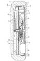
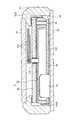
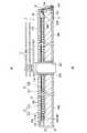
図1および図2は、本実施形態に係る時計の側断面図である。本実施形態の時計は、指針11によるアナログ時刻表示と、表示装置2によるディジタル表示とが組み合わせられたコンビネーション・ウォッチである。この時計は、地板12、この地板12に支持される駆動輪列13やステップモータ14、地板12の表示装置2側とは反対側に配置される回路基板15、および電池16などを有するムーブメント10と、ムーブメント10および表示装置2を収容するケース17と、裏蓋18と、風防ガラス19とを備えている。
なお、表示装置2とムーブメント本体101とは、パネル押さえばね101Aによって一体に組み付けられている。
回路基板15には、水晶発振回路、分周回路を含む計時回路や、制御IC、コンデンサなどが実装されている。この回路基板15は回路押さえばね101Bによってムーブメント本体101に一体に組みつけられている。1 and 2 are side sectional views of the timepiece according to the present embodiment. The timepiece of this embodiment is a combination watch in which an analog time display by the
The
A clock circuit including a crystal oscillation circuit and a frequency dividing circuit, a control IC, a capacitor, and the like are mounted on the
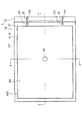
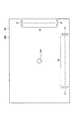
図3は、矩形状とされた表示装置2の平面模式図であり、図4は、図3のX−X´断面模式図、図5は、図3のY−Y´断面模式図である。
なお、以降の表示装置2に関する説明において、「表面」とは図4、図5等における上面をいい、「裏面」とは図4、図5等における下面をいう。3 is a schematic plan view of the
In the following description of the
表示装置2は、マトリックス駆動方式の電気泳動表示ディスプレイ(EPD;Electrophoretic Display)である表示パネル20と、表示パネル20の裏面に積層される配線基板30とを備えている。これらの表示パネル20と配線基板30とは積層されて一体にモジュール化されている。また、これらの表示パネル20および配線基板30の中心部には、指針11が固定される歯車の軸110(図4、図5)を通す貫通孔201が形成されている。この貫通孔201の周囲の部分は、エポキシ樹脂などの封止材202(図4、図5)によって封止されている。
なお、本実施形態に限らず、表示パネルはLCD(Liquid Crystal Display)や有機EL(Electro Luminescence)ディスプレイなどであってもよい。The
The display panel is not limited to this embodiment, and may be an LCD (Liquid Crystal Display), an organic EL (Electro Luminescence) display, or the like.
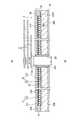
本実施形態の表示パネル20は、図4および図5に示すように、表面基板21、画像形成部としての電気泳動層22、および裏面基板としてのTFT(Thin Film Transistor)基板23の積層体である。
なお、表示パネル20は、文字、図形、画像等を表示するディジタル表示機能を有するほか、文字板としても機能する。すなわち、表示パネル20には、指針11が示すインデックスが表示される。As shown in FIGS. 4 and 5, the
The
表面基板21は、PET(ポリエチレンテレフタレート)により形成されたシート211と、シート211の裏面に成膜されたITO(Indium Tin Oxide)からなる共通電極(透明電極)212とを有しており、本実施形態では、この表面基板21に電気泳動層22を構成する多数のマイクロカプセル220が接着剤や粘着フィルム等によって固定されている。ここで、マイクロカプセル220が設けられた領域が表示パネル20の画像表示領域200(図3)に相当する。この画像表示領域200の外側は、額縁部200Zである。
なお、表面基板21の表面には、防水ガラス213が接着されている。The
A
電気泳動層22を構成するマイクロカプセル220のそれぞれの内部には、帯電した黒色の電気泳動粒子と、黒色泳動粒子とは逆極性に帯電した白色の電気泳動粒子とが格納されている。なお、図4、図5等では、マイクロカプセル220を実際の大きさよりもかなり大きく図示している。
また、電気泳動層22は、電気泳動層22の周縁部に設けられたエポキシ樹脂等による封止材24により、表面基板21とTFT基板23との間に封止されている。このように電気泳動層22が湿潤な環境から保護されることにより、電気泳動粒子の特性変化が抑制される。
封止材24は、防水ガラス213の裏面と、表面基板21の周縁部と、裏面基板23の表面とにそれぞれ密接しており、これによってシール性能が確保されている。In each of the
Further, the
The sealing
TFT基板23は、ガラス基材231と、ガラス基材231の表面に形成されたマトリックス状の画素電極、および薄膜トランジスタ等を含むTFT層232とを有している。なお、本実施形態の表示パネル20はTFT駆動方式であるが、TFD(Thin Film Diode)駆動方式などであってもよい。
TFT基板23の表面23Aには、画素電極にY方向に沿って設けられたソース線から
それぞれ引き出されたY方向駆動部232Y(図4)と、画素電極にX方向に沿って設けられたゲート線からそれぞれ引き出されたX方向駆動部232X(図5)と、共通電極212に共通電極用導通部材212A(図5)を介して導通される共通電極導通部232COM(図5)と、複数の入出力端子233(図5)とがそれぞれ形成されている。各入出力端子233は、各X方向駆動部232X、各Y方向駆動部232Y、および各共通電極導通部232COMのそれぞれに対応している。各入出力端子233は、図3に示すように、TFT基板23の一方の短辺に沿って配列されている。The
On the
配線基板30は、ガラスエポキシ製の両面基板であり、TFT基板23の裏面23Bに接着剤や粘着フィルム等によって固定されている。
配線基板30の表面30Aには、図5に示すように、ボンディングワイヤ25を介して各入出力端子233にそれぞれ導通される複数のパターン31Aが形成されている。
ボンディングワイヤ25は、TFT基板23の表面23AからTFT基板23の厚み方向に沿って裏面23B側に湾曲し、入出力端子233とパターン31Aとにそれぞれ合金接合で固定されている。
ここで、前述の封止材24は、ボンディングワイヤ25が設けられた表示パネル20の一方の短辺側では、TFT基板23の周縁部と、配線基板30の表面30Aとに亘って設けられている。これによって各ボンディングワイヤ25は互いに離間した状態で封止材24に被覆されている。The
As shown in FIG. 5, a plurality of
The
Here, the
配線基板30の裏面30Bには、表面30A側の各パターン31Aとスルーホール31Bを介してそれぞれ導通される複数の接続端子31が形成されている。これらの各接続端子31と回路基板15(図1)との間には、ラバーコネクタ32が設けられており、接続端子31はラバーコネクタ32によって回路基板15における電源ブロックや、制御回路部や、回路基板15に実装された表示パネル20の駆動回路などにそれぞれ導通されている。
ラバーコネクタ32は、詳しい図示を省略するが、各接続端子31をそれぞれ回路基板15に導通する複数の導体と、これらの導体を互いに隔てる絶縁性のラバー製の弾性体とを有している。このラバーコネクタ32がパネル押さえばね101B(図1、図2)によって配線基板30と回路基板15との間で加圧されることにより、各接続端子31と回路基板15との導通が安定する。On the
Although not shown in detail, the
以上の本実施形態によれば、次のような効果が得られる。
(1)表示装置2において、表示パネル20と配線基板30とが積層されており、TFT基板23の表面23Aの入出力端子233と接続端子31とをボンディングワイヤ25によってTFT基板23の厚み方向に沿って導通することが可能となる。このような構造の表示装置2では画像表示領域200外における表示パネル20と配線基板30との接合部が不要であり、画像表示領域200外にはボンディングワイヤ25が接触する入出力端子233および接続端子31のそれぞれの領域が確保されていればよいため、額縁部200Zを極めて狭くできる。According to the above embodiment, the following effects can be obtained.
(1) In the
(2)表示パネル20と配線基板30とが一体のモジュールとして構成されるので、時計のケース17への収納スペースを省スペース化できる。
また、このようなモジュール化により、アフターサービス時などにおける表示装置2の着脱作業が容易となる。(2) Since the
Further, such modularization facilitates the attaching / detaching operation of the
(3)配線基板30が表示パネル20に積層されたことにより、配線基板30の裏面30Bにおける任意の位置に接続端子31を形成することが可能となるので、表示装置2を様々なモデルの時計に汎用的に組み込むことが可能となる。また、端子位置の適正配置により、時計の小型化を促進できる。(3) Since the
(4)接続端子31が配線基板30の裏面30Bに形成されることによって、接続端子31と回路基板15の端子とをラバーコネクタ32を介して簡単に導通させることが可能となる。すなわち、ムーブメント10に表示装置2を載置し、パネル押さえばね101Aを地板12の外周部に係合させるだけで、ラバーコネクタ32を介して接続端子31と回路基板15とが確実に導通する。(4) By forming the
(5)入出力端子233と接続端子31との導通にボンディングワイヤ25が使用されることにより、リード線が使用される場合などと比べてTFT基板23の表面23Aに形成された入出力端子233と配線基板30の裏面30Bに形成された接続端子31とを表示パネル20の平面方向において省スペースに配線可能となる。このため、額縁部200Zをより一層狭くできる。(5) By using the
(6)封止材24が電気泳動層22の封止とボンディングワイヤ25の封止とに兼用されており、これによって構成を簡略にできる。(6) The sealing
(7)配線基板30と回路基板15とがラバーコネクタ32が間に介在した状態でパネル押さえばね101Aによって押さえられるので、接続端子31と回路基板15との導通を安定させることができる。(7) Since the
〔第1実施形態の第1変形例〕
図6は、上記第1実施形態の第1変形例に係る配線基板40の裏面40Bを示す。配線基板40の裏面40Bには、配線基板40の短辺に沿った方向に配列された第1の端子群G1としての複数の接続端子31と、配線基板40の長辺に沿った方向に配列された第2の端子群G2としての複数の接続端子31とがそれぞれ設けられている。これらの第1、第2端子群G1,G2にはそれぞれ、同じ入出力端子233に対応する接続端子31が含まれている。
このような構成によれば、複数の端子群G1,G2のうち、回路基板15の端子に接続し易い端子群を選択可能となる。すなわち、表示装置2が組み込まれる機器側の端子の位置が特定の位置に限定されないので、汎用性をより高めることができる。[First Modification of First Embodiment]
FIG. 6 shows a
According to such a configuration, a terminal group that can be easily connected to the terminal of the
〔第1実施形態の第2変形例〕
また、前述の表示装置2の裏面部には、ムーブメント10の構成部品等を設けることが可能である。すなわち、配線基板30の裏面30Bに駆動輪列13や他の輪列、レバー等を保持する押さえ板などを設けることが可能となる。これにより、表示パネル20が文字板として機能するコンビネーション時計における部品配置を効率化でき、時計の小型化を促進できる。[Second Modification of First Embodiment]
Moreover, it is possible to provide the components of the
〔第2実施形態〕
以下、本発明の第2実施形態について図7を参照して説明する。図7は、本実施形態の表示装置5の断面模式図である。表示装置5が備える配線基板50の裏面30Bには、複数の電子部品61〜64が実装されている。これらの電子部品のうち61は、表示パネル20の駆動回路ICであり、62は温度センサであり、63は指針11が固定される番車の回転位置を検出する位置検出センサを構成するフォトダイオード等の受光素子となっている。[Second Embodiment]
Hereinafter, a second embodiment of the present invention will be described with reference to FIG. FIG. 7 is a schematic cross-sectional view of the
駆動回路IC61には、配線基板50の表面30Aのパターン31Aからスルーホールを介して配線基板50の裏面30Bに取り出された複数の端子610が導通されている。なお、配線基板50の裏面30Bには、パターン31Aを介して入出力端子233のいずれかに導通された接続端子31が形成されている。
温度センサ62は、電気泳動層22が設けられた画像表示領域に対応する位置に設けられており、この温度センサ62により、電気泳動層22の温度に近い温度が検出される。この温度センサ62による検出温度に基づいて、駆動回路IC61による表示パネル20の駆動制御が実施される。A plurality of
The
本実施形態の位置検出センサは、番車の裏側の位置で回路基板15に実装されるLED(Light Emitting Diode)などの発光素子(図示省略)と、配線基板50の裏面30Bに実装され発光素子からの光を受光する受光素子63とを有している。受光素子63は、指針11が正時を示した際に番車に形成された孔を通して発光素子からの光を受光する。この指針位置の検出を受けて、計時回路で計数された内部時刻に基づいて駆動輪列を駆動制御することにより、表示時刻が修正される。
なお、位置検出センサは光式センサに限らず、ホール素子を用いた磁気式センサなどであってもよい。The position detection sensor of the present embodiment includes a light emitting element (not shown) such as an LED (Light Emitting Diode) mounted on the
The position detection sensor is not limited to an optical sensor, and may be a magnetic sensor using a Hall element.
本実施形態によれば、第1実施形態で述べた効果に加えて、次のような効果が得られる。
(8)配線基板50の裏面30Bに表示パネル20の駆動回路IC61が実装されるため、表示パネル20の駆動回路が機器側の回路基板15に実装される場合に比べて、表示パネル20と駆動回路とを接続する配線パターンの長さが短くなる。このため導通抵抗を小さくでき、これによって消費電力を低減できる。According to this embodiment, in addition to the effects described in the first embodiment, the following effects can be obtained.
(8) Since the
(9)電気泳動粒子の泳動特性は温度によって変わるが、温度センサ62による検出温度に応じて表示パネル20が駆動制御されるため、表示パネル20の表示品質を確保することが可能となる。温度センサ62は表示パネル20に一体に積層される配線基板50の裏面30Bに設けられており、この温度センサ62によって表示パネル20の温度に近い温度が検出される。すなわち、温度センサ62の検出温度に基づいて、表示パネル20の駆動制御を適切に行うことが可能となる。(9) Although the electrophoretic characteristics of the electrophoretic particles vary depending on the temperature, the
(10)表示装置5における駆動輪列13側の部分に配線基板50が配置されていることにより、位置検出センサの部品(受光素子63)を検出対象である番車の近傍に設けやすくなる。(10) Since the
なお、前述の各実施形態では、配線基板に両面基板が使用されていたが、これに限らず、配線基板に片面基板が使用されていてもよい。配線基板がスルーホールを有していない場合には、導通部材を配線基板の裏面側に取り回して入出力端子と接続端子とを導通すればよい。 In each of the above-described embodiments, the double-sided board is used as the wiring board. However, the invention is not limited to this, and a single-sided board may be used as the wiring board. When the wiring board does not have a through hole, a conductive member may be routed on the back side of the wiring board to conduct the input / output terminal and the connection terminal.
以上、本発明を実施するための最良の構成について具体的に説明したが、本発明は、これに限定されるものではない。すなわち、本発明は、主に特定の実施形態に関して特に図示され、かつ、説明されているが、本発明の技術的思想および目的の範囲から逸脱することなく、以上述べた実施形態に対し、形状、材質、数量、その他の詳細な構成において、当業者が様々な変形および改良を加えることができるものである。
上記に開示した形状、材質などを限定した記載は、本発明の理解を容易にするために例示的に記載したものであり、本発明を限定するものではないから、それらの形状、材質などの限定の一部もしくは全部の限定を外した部材の名称での記載は、本発明に含まれるものである。Although the best configuration for carrying out the present invention has been specifically described above, the present invention is not limited to this. That is, the invention has been illustrated and described primarily with respect to particular embodiments, but may be configured for the above-described embodiments without departing from the scope and spirit of the invention. Various modifications and improvements can be made by those skilled in the art in terms of materials, quantity, and other detailed configurations.
The description limiting the shape, material, etc. disclosed above is an example for easy understanding of the present invention, and does not limit the present invention. The description by the name of the member which removes a part or all of the limitation is included in the present invention.
2・・・表示装置、5・・・表示装置、10・・・ムーブメント、11・・・指針、12・・・地板、13・・・駆動輪列、15・・・回路基板、20・・・表示パネル、21・・・表面基板、22・・・電気泳動層(画像形成部)、23・・・TFT基板(裏面基板)、24・・・封止材、25・・・ボンディングワイヤ(導通部材)、30・・・配線基板、31・・・接続端子、32・・・ラバーコネクタ、40・・・配線基板、50・・・配線基板、61・・・駆動回路、62・・・温度センサ、110・・・軸、200・・・画像表示領域、200Z・・・額縁部、211・・・シート、212・・・共通電極、213・・・防水ガラス、220・・・マイクロカプセル、231・・・ガラス基材、232・・・TFT層、233・・・入出力端子、G1・・・第1の端子群、G2・・・第2の端子群。DESCRIPTION OF
Claims (10)
Translated fromJapanese前記裏面基板の裏面に積層される配線基板とを備え、
前記裏面基板の表面には、マトリックス状の画素電極、および薄膜トランジスタを含むTFT層が設けられるとともに、前記画素電極に対して、互いに直交するX方向及びY方向のうち、前記Y方向に沿って設けられたソース線からそれぞれ引き出されるY方向駆動部と、前記X方向に沿って設けられたゲート線からそれぞれ引き出されるX方向駆動部と、前記表面基板に設けられる共通電極に共通電極用導通部材を介して導通される共通電極導通部と、前記各Y方向駆動部駆動部、前記各X方向駆動部、及び前記各共通電極導通部に対応する複数の入出力端子とが形成され、
前記配線基板の裏面には、前記各入出力端子にそれぞれ導通部材によって導通される複数の接続端子が形成され、
前記画像形成部は、電気泳動粒子を含んで形成され、当該画像形成部の周縁部を含む領域に設けられる封止材によって前記表面基板と前記裏面基板との間に封止され、
前記封止材は、前記各Y方向駆動部駆動部、前記各X方向駆動部、及び前記各共通電極導通部を封止するとともに、前記導通部材を被覆する
ことを特徴とする表示装置。A display panel having a front substrate, an image forming unit, and a back substrate stacked on each other;
A wiring board laminated on the back surface of the back substrate;
Amatrix pixel electrode and a TFT layer including a thin film transistor are provided on the front surface of the back substrate, and provided along the Y direction among the X and Y directions orthogonal to the pixel electrode. A common electrode conducting member for a common electrode provided on the surface substrate; a Y-direction drive unit drawn from the source line; an X-direction drive unit drawn from the gate line provided along the X direction; a common electrode conducting portion which is conducted through the respective Y-direction driving section driving section, the respective X-direction driving section, anda plurality of output terminalscorresponding to each common electrode conducting portion is formed,
On the back surface of the wiring board, a plurality of connection terminals are formed which are electrically connected to the input / output terminals by conductive members,
The image forming unit is formed including electrophoretic particles, and is sealed between the front substrate and the back substrate by a sealing material provided in a region including a peripheral portion of the image forming unit,
The said sealing material seals each said Y direction drive part drive part, each said X direction drive part, and each said common electrode conduction | electrical_connection part, and coat | covers the said conduction member. The display apparatus characterized by the above-mentioned.
前記導通部材は、ボンディングワイヤである
ことを特徴とする表示装置。The display device according to claim 1,
The display device, wherein the conductive member is a bonding wire.
前記配線基板は、表面および裏面の両面に導電部を有する両面基板であり、
前記接続端子は、前記配線基板を貫通するスルーホールを有する
ことを特徴とする表示装置。The display device according to claim 1 or 2,
The wiring board is a double-sided board having conductive portions on both the front and back sides,
The display device, wherein the connection terminal has a through hole penetrating the wiring board.
前記配線基板の裏面には、前記表示パネルを駆動する駆動回路が実装される
ことを特徴とする表示装置。The display device according to any one of claims 1 to 3,
A display device, wherein a driving circuit for driving the display panel is mounted on a back surface of the wiring board.
前記配線基板の裏面には、温度センサが設けられる
ことを特徴とする表示装置。The display device according to any one of claims 1 to 4,
A temperature sensor is provided on the back surface of the wiring board.
当該表示装置は、機器に組み込まれ、
前記配線基板の裏面側には、前記機器が備える回路基板が配置され、
前記配線基板と前記回路基板とは、弾性を有するコネクタが間に介在した状態で近接方向に押さえられ、
前記コネクタは、前記接続端子と前記回路基板とを導通する導体と、絶縁性の弾性体とを有する
ことを特徴とする表示装置。The display device according to any one of claims 1 to 5,
The display device is incorporated in the device,
On the back side of the wiring board, a circuit board provided in the device is disposed,
The wiring board and the circuit board are pressed in the proximity direction with an elastic connector interposed therebetween,
The connector includes a conductor that conducts the connection terminal and the circuit board, and an insulating elastic body.
前記配線基板の裏面における第1の位置と第2の位置とにそれぞれ、同じ前記入出力端子に対応する複数の前記接続端子が形成され、
前記配線基板の裏面には、前記第1位置に形成された複数の接続端子からなる第1の端子群と、前記第2位置に形成された複数の接続端子からなる第2の端子群とが形成されて
いる
ことを特徴とする表示装置。The display device according to any one of claims 1 to 6,
A plurality of the connection terminals corresponding to the same input / output terminals are formed at the first position and the second position on the back surface of the wiring board, respectively.
A first terminal group including a plurality of connection terminals formed at the first position and a second terminal group including a plurality of connection terminals formed at the second position are formed on the back surface of the wiring board. A display device characterized by being formed.
前記表示装置の前記配線基板の裏面側に配置される回路基板とを備える
ことを特徴とする時計。A display device according to any one of claims 1 to 7;
A timepiece comprising: a circuit board disposed on a back surface side of the wiring board of the display device.
前記表示パネルおよび前記配線基板を厚み方向に貫通する軸に固定される指針と、
前記配線基板と前記回路基板との間に配置され、前記指針を駆動する駆動輪列とを備える
ことを特徴とする時計。The timepiece according to claim 8,
A pointer fixed to a shaft penetrating the display panel and the wiring board in a thickness direction;
A timepiece comprising a drive wheel train disposed between the wiring board and the circuit board for driving the hands.
前記配線基板の裏面には、前記駆動輪列に含まれる歯車または前記駆動輪列に連動する歯車の回転位置を検出する位置検出センサが設けられる
ことを特徴とする時計。The timepiece according to claim 9,
A timepiece having a position detection sensor for detecting a rotational position of a gear included in the driving wheel train or a gear interlocked with the driving wheel train is provided on the back surface of the wiring board.
Priority Applications (5)
| Application Number | Priority Date | Filing Date | Title |
|---|---|---|---|
| JP2007290684AJP4670855B2 (en) | 2007-11-08 | 2007-11-08 | Display device and clock |
| US12/257,942US8194222B2 (en) | 2007-11-08 | 2008-10-24 | Display device and timepiece |
| EP08019384AEP2058692B1 (en) | 2007-11-08 | 2008-11-05 | Display device and timepiece |
| CN2008101741176ACN101430473B (en) | 2007-11-08 | 2008-11-07 | Display device and timepiece |
| US13/467,690US8873015B2 (en) | 2007-11-08 | 2012-05-09 | Display device and timepiece comprising a wiring board layered on a back surface of a back substrate |
Applications Claiming Priority (1)
| Application Number | Priority Date | Filing Date | Title |
|---|---|---|---|
| JP2007290684AJP4670855B2 (en) | 2007-11-08 | 2007-11-08 | Display device and clock |
Publications (2)
| Publication Number | Publication Date |
|---|---|
| JP2009115686A JP2009115686A (en) | 2009-05-28 |
| JP4670855B2true JP4670855B2 (en) | 2011-04-13 |
Family
ID=40292635
Family Applications (1)
| Application Number | Title | Priority Date | Filing Date |
|---|---|---|---|
| JP2007290684AExpired - Fee RelatedJP4670855B2 (en) | 2007-11-08 | 2007-11-08 | Display device and clock |
Country Status (4)
| Country | Link |
|---|---|
| US (2) | US8194222B2 (en) |
| EP (1) | EP2058692B1 (en) |
| JP (1) | JP4670855B2 (en) |
| CN (1) | CN101430473B (en) |
Families Citing this family (22)
| Publication number | Priority date | Publication date | Assignee | Title |
|---|---|---|---|---|
| WO2005095967A1 (en) | 2004-03-23 | 2005-10-13 | Quidel Corporation | Hybrid phase lateral flow assay |
| DE102008028803A1 (en)* | 2008-06-19 | 2009-12-24 | Raytheon Anschütz Gmbh | Method for driving stepper motors |
| JP2010066564A (en)* | 2008-09-11 | 2010-03-25 | Seiko Epson Corp | Electrophoretic display device, manufacturing method therefor, and wristwatch |
| JP5435233B2 (en)* | 2010-03-11 | 2014-03-05 | セイコーエプソン株式会社 | Electrophoretic display device, clock, electronic device |
| JP2012220635A (en) | 2011-04-06 | 2012-11-12 | Sony Corp | Display device and electronic apparatus |
| US10261370B2 (en) | 2011-10-05 | 2019-04-16 | Apple Inc. | Displays with minimized border regions having an apertured TFT layer for signal conductors |
| US9286826B2 (en) | 2011-10-28 | 2016-03-15 | Apple Inc. | Display with vias for concealed printed circuit and component attachment |
| US9226347B2 (en) | 2012-06-25 | 2015-12-29 | Apple Inc. | Displays with vias |
| US9214507B2 (en) | 2012-08-17 | 2015-12-15 | Apple Inc. | Narrow border organic light-emitting diode display |
| US9454025B2 (en) | 2012-08-31 | 2016-09-27 | Apple Inc. | Displays with reduced driver circuit ledges |
| KR102282105B1 (en) | 2012-09-03 | 2021-07-26 | 가부시키가이샤 한도오따이 에네루기 켄큐쇼 | Display device and electronic device |
| JP6310216B2 (en)* | 2013-09-06 | 2018-04-11 | キヤノン株式会社 | Radiation detection apparatus, manufacturing method thereof, and radiation detection system |
| JP6403089B2 (en)* | 2014-08-28 | 2018-10-10 | カシオ計算機株式会社 | Board connection structure and electronic equipment |
| KR102386706B1 (en)* | 2015-06-11 | 2022-04-14 | 삼성디스플레이 주식회사 | Display device and watch having the same |
| KR20170039388A (en)* | 2015-10-01 | 2017-04-11 | 엘지전자 주식회사 | Electronic device |
| CN205210522U (en)* | 2015-10-27 | 2016-05-04 | 歌尔声学股份有限公司 | Smart watch |
| JP6891393B2 (en) | 2015-12-17 | 2021-06-18 | イー インク コーポレイション | Electrophoresis display device and electronic equipment |
| EP3474085B1 (en)* | 2017-10-23 | 2020-03-25 | ETA SA Manufacture Horlogère Suisse | Control device provided with a module for detecting the axial position of the stem thereof, and timepiece comprising such a control device |
| US12016228B2 (en)* | 2018-09-28 | 2024-06-18 | Sharp Kabushiki Kaisha | Display device and display device production method |
| US20240170498A1 (en)* | 2021-03-26 | 2024-05-23 | Kyocera Corporation | Display device |
| CN114200727A (en)* | 2021-12-20 | 2022-03-18 | 昆山龙腾光电股份有限公司 | Substrate convenient for hole opening design and display device |
| US20230351934A1 (en) | 2022-04-28 | 2023-11-02 | E Ink Holdings Inc. | Narrow border reflective display device |
Family Cites Families (26)
| Publication number | Priority date | Publication date | Assignee | Title |
|---|---|---|---|---|
| JPS55154485A (en) | 1979-05-21 | 1980-12-02 | Seiko Instr & Electronics Ltd | Electronic wristwatch |
| JPS6078188A (en) | 1983-10-03 | 1985-05-02 | 三菱アルミニウム株式会社 | Composite pipe material for heat exchanger made of al alloy having excellent hole corrosion resistance |
| JPS6078188U (en)* | 1983-11-02 | 1985-05-31 | ジエコー株式会社 | Display element circuit board |
| US4598960A (en)* | 1985-04-29 | 1986-07-08 | Copytele, Inc. | Methods and apparatus for connecting closely spaced large conductor arrays employing multi-conductor carrier boards |
| JPH0444148U (en)* | 1990-08-20 | 1992-04-15 | ||
| WO1997001791A1 (en)* | 1995-06-29 | 1997-01-16 | Philips Electronics N.V. | Display device |
| TW410534B (en) | 1997-07-16 | 2000-11-01 | Matsushita Electric Industrial Co Ltd | Wiring board and production process for the same |
| JPH1152406A (en)* | 1997-08-04 | 1999-02-26 | Alps Electric Co Ltd | Liquid crystal display device |
| US6069679A (en)* | 1997-09-04 | 2000-05-30 | Motorola, Inc. | Selective call receiver having a display module with integrated circuits and method therefor |
| JP4298068B2 (en) | 1998-08-18 | 2009-07-15 | セイコーエプソン株式会社 | ELECTRO-OPTICAL DEVICE, ELECTRONIC DEVICE EQUIPPED WITH THE SAME, AND METHOD FOR PRODUCING ELECTRO-OPTICAL DEVICE |
| US6498636B1 (en)* | 1999-03-30 | 2002-12-24 | National Semiconductor Corporation | Apparatus and method for substantially stress-free electrical connection to a liquid crystal display |
| US20020085158A1 (en) | 1999-05-17 | 2002-07-04 | Karl M. Armagost | Ball grid array mounted liquid crystal display panels |
| JP3540255B2 (en) | 1999-09-28 | 2004-07-07 | シャープ株式会社 | Method for repairing conduction failure of liquid crystal display device |
| KR100530911B1 (en)* | 1999-10-01 | 2005-11-23 | 세이코 엡슨 가부시키가이샤 | Wiring board, semiconductor device and method of producing, testing and packaging the same, and circuit board and electronic equipment |
| JP4455724B2 (en)* | 2000-04-19 | 2010-04-21 | シチズンホールディングス株式会社 | clock |
| JP3598994B2 (en)* | 2000-07-10 | 2004-12-08 | セイコーエプソン株式会社 | Manufacturing method of electro-optical device |
| CN1292299C (en)* | 2001-06-29 | 2006-12-27 | 西铁城时计株式会社 | Liquid crystal display panel and manufacturing method thereof |
| AU2003219401A1 (en)* | 2002-05-06 | 2003-11-17 | Koninklijke Philips Electronics N.V. | Electrophoretic display device |
| JP4259084B2 (en) | 2002-10-16 | 2009-04-30 | セイコーエプソン株式会社 | Display body structure, display body structure manufacturing method, and electronic apparatus |
| US7015893B2 (en)* | 2003-01-31 | 2006-03-21 | Motorola, Inc. | Photoluminescent electrophoretic display |
| JP4217090B2 (en)* | 2003-03-20 | 2009-01-28 | 株式会社 日立ディスプレイズ | Display device |
| KR20060017521A (en)* | 2003-05-23 | 2006-02-23 | 코닌클리케 필립스 일렉트로닉스 엔.브이. | Improved Drive System for Electrophoretic Displays |
| JP2007505348A (en)* | 2003-09-08 | 2007-03-08 | コニンクリユケ フィリップス エレクトロニクス エヌ.ブイ. | Driving an electrophoretic display using symmetrical data frames |
| JP4285484B2 (en)* | 2005-01-24 | 2009-06-24 | セイコーエプソン株式会社 | ELECTRO-OPTICAL DEVICE, ELECTRO-OPTICAL DEVICE SUBSTRATE, CIRCUIT BOARD, MOUNTING STRUCTURE, AND ELECTRONIC DEVICE |
| JP2007133182A (en) | 2005-11-10 | 2007-05-31 | Seiko Epson Corp | Electrophoretic display module and electrophoretic display device |
| JP2007285748A (en)* | 2006-04-13 | 2007-11-01 | Seiko Epson Corp | Watches |
- 2007
- 2007-11-08JPJP2007290684Apatent/JP4670855B2/ennot_activeExpired - Fee Related
- 2008
- 2008-10-24USUS12/257,942patent/US8194222B2/ennot_activeExpired - Fee Related
- 2008-11-05EPEP08019384Apatent/EP2058692B1/ennot_activeNot-in-force
- 2008-11-07CNCN2008101741176Apatent/CN101430473B/ennot_activeExpired - Fee Related
- 2012
- 2012-05-09USUS13/467,690patent/US8873015B2/ennot_activeExpired - Fee Related
Also Published As
| Publication number | Publication date |
|---|---|
| CN101430473A (en) | 2009-05-13 |
| US20090122653A1 (en) | 2009-05-14 |
| JP2009115686A (en) | 2009-05-28 |
| EP2058692B1 (en) | 2011-10-05 |
| US20120218502A1 (en) | 2012-08-30 |
| EP2058692A1 (en) | 2009-05-13 |
| US8194222B2 (en) | 2012-06-05 |
| US8873015B2 (en) | 2014-10-28 |
| CN101430473B (en) | 2012-02-15 |
Similar Documents
| Publication | Publication Date | Title |
|---|---|---|
| JP4670855B2 (en) | Display device and clock | |
| JP4353266B2 (en) | Electro-optical device and electronic apparatus | |
| US8379163B2 (en) | Display device | |
| WO2006126376A1 (en) | Liquid crystal display | |
| JP2010061027A (en) | Liquid crystal display device | |
| US20170212395A1 (en) | Liquid crystal display device | |
| KR20090101838A (en) | Mounting structure, electro-optical device, and electronic apparatus | |
| US20180180797A1 (en) | Display device circuit board, display device, and electronic device | |
| JP2007273578A (en) | Electronic component connection structure | |
| CN1963653A (en) | Electrophoretic display module and electrophoretic display device | |
| CN1312521C (en) | Electrooptical apparatus and its mfg. method and electronic device with the same | |
| JP2008277047A (en) | Surface light source device and liquid crystal display device | |
| JP2006235252A (en) | Display device | |
| JP2007086408A (en) | Electrooptical device, method for manufacturing electrooptical device, and electronic equipment | |
| JP2008026534A (en) | Electro-optical device and electronic apparatus | |
| JP4296877B2 (en) | Electro-optical device and electronic apparatus including the electro-optical device | |
| JP4564435B2 (en) | Display device | |
| JP2007292826A (en) | Liquid crystal module | |
| KR101137881B1 (en) | liquid crystal display device | |
| JP2001166328A (en) | Electrode connection structure of liquid crystal display panel | |
| JP2011203398A (en) | Electrophoretic display device, clock, and electronic device | |
| JP2006317821A (en) | Liquid crystal display device | |
| JP2011059339A (en) | Liquid crystal display device | |
| JP4060634B2 (en) | Liquid crystal display | |
| JP2011191160A (en) | Time piece |
Legal Events
| Date | Code | Title | Description |
|---|---|---|---|
| A977 | Report on retrieval | Free format text:JAPANESE INTERMEDIATE CODE: A971007 Effective date:20091007 | |
| A131 | Notification of reasons for refusal | Free format text:JAPANESE INTERMEDIATE CODE: A131 Effective date:20091020 | |
| A521 | Request for written amendment filed | Free format text:JAPANESE INTERMEDIATE CODE: A523 Effective date:20091211 | |
| A131 | Notification of reasons for refusal | Free format text:JAPANESE INTERMEDIATE CODE: A131 Effective date:20100119 | |
| A521 | Request for written amendment filed | Free format text:JAPANESE INTERMEDIATE CODE: A523 Effective date:20100323 | |
| TRDD | Decision of grant or rejection written | ||
| A01 | Written decision to grant a patent or to grant a registration (utility model) | Free format text:JAPANESE INTERMEDIATE CODE: A01 Effective date:20101221 | |
| A01 | Written decision to grant a patent or to grant a registration (utility model) | Free format text:JAPANESE INTERMEDIATE CODE: A01 | |
| A61 | First payment of annual fees (during grant procedure) | Free format text:JAPANESE INTERMEDIATE CODE: A61 Effective date:20110103 | |
| R150 | Certificate of patent or registration of utility model | Ref document number:4670855 Country of ref document:JP Free format text:JAPANESE INTERMEDIATE CODE: R150 Free format text:JAPANESE INTERMEDIATE CODE: R150 | |
| FPAY | Renewal fee payment (event date is renewal date of database) | Free format text:PAYMENT UNTIL: 20140128 Year of fee payment:3 | |
| S531 | Written request for registration of change of domicile | Free format text:JAPANESE INTERMEDIATE CODE: R313531 | |
| R350 | Written notification of registration of transfer | Free format text:JAPANESE INTERMEDIATE CODE: R350 | |
| LAPS | Cancellation because of no payment of annual fees |