JP4660163B2 - Semiconductor memory device - Google Patents
Semiconductor memory deviceDownload PDFInfo
- Publication number
- JP4660163B2 JP4660163B2JP2004316043AJP2004316043AJP4660163B2JP 4660163 B2JP4660163 B2JP 4660163B2JP 2004316043 AJP2004316043 AJP 2004316043AJP 2004316043 AJP2004316043 AJP 2004316043AJP 4660163 B2JP4660163 B2JP 4660163B2
- Authority
- JP
- Japan
- Prior art keywords
- memory cell
- data
- information
- bit line
- potential
- Prior art date
- Legal status (The legal status is an assumption and is not a legal conclusion. Google has not performed a legal analysis and makes no representation as to the accuracy of the status listed.)
- Expired - Fee Related
Links
Images


Classifications
- G—PHYSICS
- G11—INFORMATION STORAGE
- G11C—STATIC STORES
- G11C11/00—Digital stores characterised by the use of particular electric or magnetic storage elements; Storage elements therefor
- G11C11/21—Digital stores characterised by the use of particular electric or magnetic storage elements; Storage elements therefor using electric elements
- G11C11/34—Digital stores characterised by the use of particular electric or magnetic storage elements; Storage elements therefor using electric elements using semiconductor devices
- G11C11/40—Digital stores characterised by the use of particular electric or magnetic storage elements; Storage elements therefor using electric elements using semiconductor devices using transistors
- G11C11/401—Digital stores characterised by the use of particular electric or magnetic storage elements; Storage elements therefor using electric elements using semiconductor devices using transistors forming cells needing refreshing or charge regeneration, i.e. dynamic cells
- G11C11/403—Digital stores characterised by the use of particular electric or magnetic storage elements; Storage elements therefor using electric elements using semiconductor devices using transistors forming cells needing refreshing or charge regeneration, i.e. dynamic cells with charge regeneration common to a multiplicity of memory cells, i.e. external refresh
- G11C11/404—Digital stores characterised by the use of particular electric or magnetic storage elements; Storage elements therefor using electric elements using semiconductor devices using transistors forming cells needing refreshing or charge regeneration, i.e. dynamic cells with charge regeneration common to a multiplicity of memory cells, i.e. external refresh with one charge-transfer gate, e.g. MOS transistor, per cell
- G—PHYSICS
- G11—INFORMATION STORAGE
- G11C—STATIC STORES
- G11C11/00—Digital stores characterised by the use of particular electric or magnetic storage elements; Storage elements therefor
- G11C11/21—Digital stores characterised by the use of particular electric or magnetic storage elements; Storage elements therefor using electric elements
- G11C11/34—Digital stores characterised by the use of particular electric or magnetic storage elements; Storage elements therefor using electric elements using semiconductor devices
- G11C11/40—Digital stores characterised by the use of particular electric or magnetic storage elements; Storage elements therefor using electric elements using semiconductor devices using transistors
- G11C11/401—Digital stores characterised by the use of particular electric or magnetic storage elements; Storage elements therefor using electric elements using semiconductor devices using transistors forming cells needing refreshing or charge regeneration, i.e. dynamic cells
- G11C11/4063—Auxiliary circuits, e.g. for addressing, decoding, driving, writing, sensing or timing
- G11C11/407—Auxiliary circuits, e.g. for addressing, decoding, driving, writing, sensing or timing for memory cells of the field-effect type
- G11C11/409—Read-write [R-W] circuits
- G11C11/4099—Dummy cell treatment; Reference voltage generators
- G—PHYSICS
- G11—INFORMATION STORAGE
- G11C—STATIC STORES
- G11C2211/00—Indexing scheme relating to digital stores characterized by the use of particular electric or magnetic storage elements; Storage elements therefor
- G11C2211/401—Indexing scheme relating to cells needing refreshing or charge regeneration, i.e. dynamic cells
- G11C2211/4016—Memory devices with silicon-on-insulator cells
Landscapes
- Engineering & Computer Science (AREA)
- Microelectronics & Electronic Packaging (AREA)
- Computer Hardware Design (AREA)
- Dram (AREA)
Description
Translated fromJapanese本発明は半導体記憶装置に関する。 The present invention relates to a semiconductor memory device.
FBC(Floating Body Cell)メモリは、SOI基板上に形成される揮発性メモリであり、トランジスタのフローティングボディにホールが蓄積されているか否かによってデータ“1”または“0”を記憶するメモリである。メモリセルに記憶されたデータ“1”または“0”を識別するために、データ“1”を記憶する基準メモリセルおよびデータ“0”を記憶する基準メモリセルをショートさせることによってデータ“1”とデータ“0”との中間電位を有する基準電位を生成する。センスアンプは、或る情報を格納するメモリセルから読み出されたデータの電位と基準電位とを比較する。これにより、メモリセルに記憶されたデータが“1”または“0”であることを識別することができる。 An FBC (Floating Body Cell) memory is a volatile memory formed on an SOI substrate and stores data “1” or “0” depending on whether holes are accumulated in the floating body of a transistor. . In order to identify the data “1” or “0” stored in the memory cell, the reference memory cell that stores the data “1” and the reference memory cell that stores the data “0” are short-circuited. And a reference potential having an intermediate potential between “0” and data “0”. The sense amplifier compares the potential of data read from a memory cell storing certain information with a reference potential. As a result, it can be identified that the data stored in the memory cell is “1” or “0”.
このように基準電位の生成のために、データ“1” を格納した基準メモリセルおよびデータ“0” を格納した基準メモリセルが必要である。 Thus, in order to generate the reference potential, a reference memory cell storing data “1” and a reference memory cell storing data “0” are required.
一般に、FBCメモリセルは、データ“1”の場合には、すでにフローティングボディにホールが蓄積されているのでリテンションの影響を受けない。しかし、データ“0”の場合には、リテンションによりフローティングボディ内にホールが徐々に入り込んでくるため、データが“1”に変化してしまう。このように、FBCメモリセルは、情報を格納するメモリセルだけでなく、基準メモリセルに使用しているデータ“0”の基準メモリセルもリテンションの影響を受ける。そのため、リテンションによる基準電位変動を防止するためにリフレッシュ動作を必要とする。したがって、半導体記憶装置の消費電力の低減が困難であるという問題が生じていた。In general, in the case of data “1”, the FBC memory cell is not affected byretention because holes are already accumulated in the floating body. However, in the case of data “0”, the holes gradually enter the floating body due toretention , so that the data changes to “1”. As described above, in the FBC memory cell, not only the memory cell storing information but also the reference memory cell of data “0” used for the reference memory cell is affected by theretention . For this reason, a refresh operation is required to prevent a reference potential fluctuation due toretention . Therefore, there has been a problem that it is difficult to reduce the power consumption of the semiconductor memory device.
また、データ“1”を格納した基準メモリセルおよびデータ“0”を格納した基準メモリセルを用いて基準電位を生成すると、基準電位がばらつく。この基準電位のばらつきは、データ“1”の基準メモリセルのばらつきとデータ“0”の基準メモリセルのばらつきの平均である。基準電位のばらつきが大きいと、基準電位のばらつきの範囲がメモリセルのばらつきの範囲と重複する場合が生じる。これは、半導体記憶装置の歩留まりに悪影響を及ぼす。従って、基準電位のばらつきの範囲がメモリセルのばらつきの範囲と重複しないように、データ“1”とデータ“0”との間の電位差の幅を大きくする必要がある。しかし、半導体記憶装置が益々微細化されている状況の下で、データ“1”とデータ“0”との間の電位差の幅を大きくすることは困難である。
ばらつきが少ない基準電位を生成し尚且つリフレッシュ動作を必要としない基準メモリセルを備えた半導体記憶装置を提供することである。 To provide a semiconductor memory device including a reference memory cell that generates a reference potential with little variation and does not require a refresh operation.
本発明に係る実施形態に従った半導体記憶装置は、電気的に浮遊状態のボディに電荷が蓄積された状態を示す第1のデータ、もしくは、前記ボディに電荷が蓄積されていない状態を示す第2のデータを記憶する複数の情報メモリセルがマトリクス状に配置されたメモリセルアレイと、前記メモリセルアレイの各行の前記情報メモリセルに接続された情報ワード線と、前記メモリセルアレイの各列の前記情報メモリセルに接続された情報ビット線と、前記情報メモリセルのデータを判別するために用いられる基準電位を電源との間で生成し、前記第1のデータのみを格納する基準メモリセルと、前記基準メモリセルに接続された基準ビット線と、前記情報ビット線および前記基準ビット線に接続されたセンスアンプとを備え、
データのリテンション時において、前記情報メモリセルはリフレッシュ動作の対象であり、前記基準メモリセルには前記リフレッシュ動作を行うことなしに前記第1のデータが保持されており、
前記情報メモリセルからデータを読み出すときに、前記情報ワード線は、
Vt1≦Vg≦Vt0
(Vgは前記情報ワード線の電位、Vt1は前記第1のデータを格納する前記情報メモリセルの閾値電圧、Vt0は前記第2のデータを格納する前記情報メモリセルの閾値電圧)
を満たすことを特徴とする。In the semiconductor memory device according to the embodiment of the present invention,the first data indicating a state in which chargesare accumulated in the electrically floating body, or the first state in which no charges are accumulated in the body. A memory cell array in which a plurality of information memory cells storingtwo data are arranged in a matrix, an information word line connected to the information memory cells in each row of the memory cell array, and the information in each column of the memory cell array A reference memory cellthat generatesa reference potential used for discriminating data of the information bit line connected to the memory cell and data of the information memory cell, and storesonly the first data; and A reference bit line connected to a reference memory cell; and a sense amplifier connected to the information bit line and the reference bit line;
At the time of data retention, theinformation memory cell is a target of a refresh operation, and the first data is held in the reference memory cell without performing the refresh operation,
When reading data from the information memory cell, the information word line is
Vt1 ≦ Vg ≦ Vt0
(Vg is the potential of the information word line, Vt1 is the threshold voltage of the information memory cell storing the first data, and Vt0 is the threshold voltage of the information memory cell storing the second data)
It is characterizedby satisfying .
本発明に係る他の実施形態に従った半導体記憶装置は、電気的に浮遊状態のボディに電荷が蓄積された状態を示す第1のデータ、もしくは、前記ボディに電荷が蓄積されていない状態を示す第2のデータを記憶する複数の情報メモリセルがマトリクス状に配置されたメモリセルアレイと、前記メモリセルアレイの各行に接続された情報ワード線と、前記メモリセルアレイの各列に接続されたビット線と、前記メモリセルのデータを判別するために用いられる基準電圧を電源との間で生成し、前記第1のデータのみを格納し、同一メモリセルアレイ内において2本の前記ビット線ごとに1つずつ設けられた基準メモリセルと、同一メモリセルアレイ内において隣接する2本の前記ビット線間に接続され、前記基準電圧を生成するときに導通状態になる平均化トランジスタと、2つの前記メモリセルアレイのそれぞれに含まれる2本のビット線に接続され、該2本のビット線のうち一方のビット線から前記情報メモリセルのデータを受け、他方のビット線から前記基準メモリセルおよび前記平均化トランジスタによって生成された前記基準電圧を受け、該基準電圧に基づいて前記情報メモリセルからのデータを検出するセンスアンプとを備え、
データのリテンション時において、前記情報メモリセルはリフレッシュ動作の対象であり、前記基準メモリセルには前記リフレッシュ動作を行うことなしに前記第1のデータが保持されており、
前記情報メモリセルからデータを読み出すときに、前記情報ワード線は、
Vt1≦Vg≦Vt0
(Vgは前記情報ワード線の電位、Vt1は前記第1のデータを格納する前記情報メモリセルの閾値電圧、Vt0は前記第2のデータを格納する前記情報メモリセルの閾値電圧)
を満たすことを特徴とする。A semiconductor memory device according to another embodiment of the present invention hasa first data indicating a state in which chargesare accumulated in an electrically floating body, or a state in which no charges are accumulated in the body. A memory cell array in which a plurality ofinformation memory cells storingsecond data shown are arranged in a matrix, an information word line connected to each row of the memory cell array, and a bit line connected to each column of the memory cell array And a reference voltage used to determine data of the memory cellis generatedbetween the power supply ,the first data only is stored, andone for each of thetwo bit lines in thesame memory cell array. a reference memory cells providedbybeing connected between two of said bit lines adjacent in the same memory cell array, a conductive state when generating the reference voltage An averaging transistor comprising, connected to thetwo bit linesincluded in each of two of said memory cell array,receives the data of the information memory cell from one of the bit lines of the two bit lines, the other bit A sense amplifierthat receives the reference voltage generated by the reference memory cell and the averaging transistor from a line and detects data from the information memory cell based on the reference voltage ;
At the time of data retention, theinformation memory cell is a target of a refresh operation, and the first data is held in the reference memory cell without performing the refresh operation,
When reading data from the information memory cell, the information word line is
Vt1 ≦ Vg ≦ Vt0
(Vg is the potential of the information word line, Vt1 is the threshold voltage of the information memory cell storing the first data, and Vt0 is the threshold voltage of the information memory cell storing the second data)
It is characterizedby satisfying .
本発明による半導体記憶装置は、電位のばらつきが少ない基準データを生成することができ尚且つリフレッシュ動作を必要としない基準メモリセルを備える。 The semiconductor memory device according to the present invention includes a reference memory cell that can generate reference data with little potential variation and does not require a refresh operation.
以下、図面を参照して本発明に係る実施形態を説明する。本実施形態は、本発明を限定するものではない。本発明に係る実施形態は、単一種類のデジタルデータ“1”で基準電位を生成する。これにより、リテンションによる基準メモリセルのデータ劣化を防止し、基準電位のばらつきを小さくすることができる。 Embodiments according to the present invention will be described below with reference to the drawings. This embodiment does not limit the present invention. The embodiment according to the present invention generates a reference potential using a single type of digital data “1”. As a result, data deterioration of the reference memory cell due to retention can be prevented, and variations in the reference potential can be reduced.
(第1の実施形態)
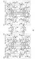
図1は、本発明に係る第1の実施形態に従った半導体記憶装置100の部分的な回路図である。半導体記憶装置100は、情報メモリセルMC(以下、単に、メモリセルともいう)、情報ワード線(以下、単に、ワード線ともいう)WL0〜WLm、情報ビット線(以下、単に、ビット線ともいう)BL0〜BLn、基準メモリセルDMC0、基準ビット線DBL0、DBL1、センスアンプSA0〜SAn、選択トランジスタTBS0〜TBSn、クランプトランジスタTFAITおよび負荷電流トランジスタTCL0、TCL1を備えている。mおよびnは自然数である。(First embodiment)
FIG. 1 is a partial circuit diagram of a
メモリセルアレイMCAは、マトリクス状に配置されたメモリセルMCの配列である。メモリセルMCは、データの書込み/読出しが可能なn型のFBCメモリセルである。本実施形態では、メモリセルMCのデータは、フローティングボディ(図示せず)にホールを蓄積した状態がデータ“1”であり、メモリセルMCのフローティングボディにホールが蓄積されていない状態がデータ“0”である。このとき、データ“1”を格納するメモリセルMCの閾値電圧Vt1は、データ“0”を格納するメモリセルMCの閾値電圧Vt0よりも低くなる。この閾値電圧Vt1とVt0との差によるメモリセルMCに流れる電流差を電圧変換し、この電圧差によってセンスアンプSAでデータを判別する。また、データの読出し時には、例えば、ワード線に1.5Vを印加し、並びに、ビット線に0.2Vを印加することによって、メモリセルMCを線形領域で駆動させる。The memory cell array MCA is an array of memory cells MC arranged in a matrix. Memory cell MC is an n-type FBC memory cell capable of writing / reading data. In this embodiment, the data of the memory cell MC is data “1” when holes are accumulated in a floating body (not shown), and data “No” is accumulated when holes are not accumulated in the floating body of the memory cell MC. 0 ". At this time, the threshold voltage Vt1 of the memory cell MC storing the data “1” is lower than the threshold voltageVt0 of the memory cell MC storing the data “0”. A current difference flowing through the memory cell MC due to the difference between the threshold voltages Vt1 andVt0 is converted into a voltage, and data is discriminated by the sense amplifier SA based on the voltage difference. At the time of reading data, for example, 1.5 V is applied to the word line and 0.2 V is applied to the bit line to drive the memory cell MC in the linear region.
ワード線WL0〜WLmは、それぞれメモリセルアレイMCAの行方向に配列されたメモリセルMCのゲートに接続されている。ビット線BL0〜BLnは、それぞれメモリセルアレイMCAの列方向に配列されたメモリセルMCのゲートに接続されている。尚、本実施形態では、ワード線WL0〜WLmが延伸する方向を行方向とし、ビット線BL0〜BLnが延伸する方向を列方向としている。 The word lines WL0 to WLm are connected to the gates of the memory cells MC arranged in the row direction of the memory cell array MCA, respectively. The bit lines BL0 to BLn are respectively connected to the gates of the memory cells MC arranged in the column direction of the memory cell array MCA. In the present embodiment, the direction in which the word lines WL0 to WLm extend is the row direction, and the direction in which the bit lines BL0 to BLn extend is the column direction.
センスアンプSA0〜SAnは、ビット線BL0〜BLnのそれぞれに対して設けられており、メモリセルMC内のデータを検出する。選択トランジスタTBS0〜TBSnは、それぞれビット線BL0〜BLnと各センスアンプSA0〜SAnとの間に接続されている。The sense amplifiers SA0 to SAn are provided for the bit lines BL0 to BLn, respectively, and detect data in the memory cells MC. The select transistors TBS0 to TBSn are connected between the bit lines BL0 to BLn and the sense amplifiers SA0 to SAn, respectively.
メモリセルMCのデータを読み出すときには、ワード線WL0〜WLmのいずれかに電圧を印加するとともに、選択トランジスタTBS0〜TBSnのいずれかをオンすることによってビット線BL0〜BLnのいずれかをセンスアンプの一方の入力に接続する。例えば、ビット線WL1およびビット線BL1を選択した場合、メモリセルMCSが選択される。選択トランジスタTBS1をオンにすることによって、メモリセルMCSがセンスアンプSA1に接続される。さらに、負荷電流トランジスタTCL1がオンすることによって、電源V0がメモリセルMCSと接続され、メモリセルMCSに電流Iが流れる。これにより、メモリセルMCSのデータ(“0”または“1”)に依存した電位がセンスアンプSA1の一方の入力に伝達される。When reading the data of the memory cell MC, the sense amplifier of any of the bit lines BL0~BLn by applies a voltage to one of word lines WL0 to WLm, to turn on one of the selection transistorsT BS0through T BSn Connect to one of the inputs. For example, when the bit line WL1 and the bit line BL1 are selected, the memory cell MCS is selected. By turning on the selection transistorT BS1, the memory cell MCS is connected to the sense amplifier SA1. Further, when the load current transistorTCL1 is turned on, the power source V0 is connected to the memory cell MCS, and a current I flows through the memory cell MCS. As a result, a potential depending on the data (“0” or “1”) of the memory cell MCS is transmitted to one input of the sense amplifier SA1.
ここで、ワード線に印加する駆動電圧Vgは、データ“1”を格納するメモリセルMCの閾値電圧Vt1以上かつデータ“0”を格納するメモリセルMCの閾値電圧Vt0以下の電圧であることに注意されたい。即ち、駆動電圧Vgは式1を満たす。 Here, the drive voltage Vg applied to the word line is a voltage not lower than the threshold voltage Vt1 of the memory cell MC storing data “1” and not higher than the threshold voltage Vt0 of the memory cell MC storing data “0”. Please be careful. That is, the drive voltage Vg satisfies the
Vt1≦Vg≦Vt0 (式1)
駆動電圧Vgが閾値電圧Vt0以下であるので、メモリセルMCSのデータが“0”である場合には、メモリセルMCSはオンしない。よって、データ“0”を搬送するビット線の電位は、電源電圧と等しいV0となる。一方、駆動電圧Vgは閾値電圧Vt1以上であるので、メモリセルMCSのデータが“1”である場合には、メモリセルMCSはオンする。よって、データ“1”を搬送するビット線の電位は、電源電圧V0よりも低いV1となる。式1を満たす電圧Vgをワード線に印加する理由は図2を参照して後述される。Vt1 ≦ Vg ≦ Vt0 (Formula 1)
Since the drive voltage Vg is equal to or lower than the threshold voltage Vt0 , the memory cell MCS is not turned on when the data in the memory cell MCS is “0”. Therefore, the potential of the bit line carrying data “0” is V0 equal to the power supply voltage. On the other hand, since thedrive voltage Vg is equal to or higher than thethreshold voltage Vt1 , when the data in the memory cell MCS is “1”, the memory cell MCS is turned on. Therefore, the potential of the bit line carrying data “1” is V1 lower than the power supply voltage V0. The reason why the voltage Vg
尚、このときクランプトランジスタTFAITは、ビット線BL0〜BLnの電位が過剰に上昇することを防止するために設けられている。クランプトランジスタTFAITは、常時オンと考えて良い。At this time, the clamp transistor TFAIT is provided in order to prevent the potential of the bit lines BL0 toBLn from rising excessively. The clamp transistor TFAIT may be considered always on.
メモリセルアレイMCAは、基準メモリセルDMC0、DMC1をさらに含む。基準メモリセルDMC0は、情報メモリセルMCと同じ構成を有し、列方向に配列されている。基準メモリセルDMC0は、ワード線WL0〜WLmのそれぞれに対して設けられている。基準メモリセルDMC0の各ゲートはそれぞれワード線WL0〜WLmに接続されている。基準メモリセルDMC0のドレインは基準ビット線DBL0に共通に接続されている。リテンションによるデータ劣化を防止するために単一種類のデジタルデータとして“1”が基準メモリセルDMC0に格納されている。基準電位は、メモリセルMCのデータを判別するために用いられる基準データの電位である。Memory cell array MCA further includes reference memory cells DMC0 and DMC1. The reference memory cell DMC0 has the same configuration as the information memory cell MC and is arranged in the column direction. The reference memory cell DMC0 is provided for each of the word lines WL0 to WLm. Each gate of the reference memory cell DMC0 is connected to each of the word lines WL0 to WLm. The drain of the reference memory cell DMC0 is commonly connected to the reference bit line DBL0.In order to preventdata deterioration due toretention , “1” is stored in the reference memory cell DMC0 as a single kind of digital data. The reference potential is a reference data potential used to determine data in the memory cell MC.
基準メモリセルDMC1は、半導体記憶装置100の動作に関係しないので、存在しなくてもよい。さらに、図1では、基準メモリセルDMC1と基準ビット線DBL1とが切断されているが、基準メモリセルDMC1とグランドとが切断されていてもよい。 Since the reference memory cell DMC1 is not related to the operation of the
選択トランジスタTDBS0、TDBS1は、それぞれ基準ビット線DBL0、DBL1とセンスアンプSAとの間に接続されている。データの読出し時に選択トランジスタTDBS0およびTDBS1がともにオンする。これにより2本の基準ビット線DBL0およびDBL1がセンスアンプSAの他方の入力に接続される。例えば、ビット線WL1を選択した場合、基準メモリセルDMCSが選択される。この場合、基準メモリセルDMCSがセンスアンプSAの他方の入力に電気的に接続される。さらに、負荷電流トランジスタTDCL0およびTDCL1がオンすることによって、2つの電源V0が基準メモリセルDMCSに並列に接続される。The selection transistors TDBS0 and TDBS1 are connected between the reference bit lines DBL0 and DBL1 and the sense amplifier SA, respectively. When reading data, both the select transistors TDBS0 and TDBS1 are turned on. As a result, the two reference bit lines DBL0 and DBL1 are connected to the other input of the sense amplifier SA. For example, when the bit line WL1 is selected, the reference memory cell DMCS is selected. In this case, the reference memory cell DMCS is electrically connected to the other input of the sense amplifier SA. Further, when the load current transistors TDCL0 and TDCL1 are turned on, the two power sources V0 are connected in parallel to the reference memory cell DMCS.
ここで、上述のとおり、ワード線に印加する駆動電圧Vgは式1を満たす。基準メモリセルDMC0はデータ“1”を格納しているので、基準メモリセルDMC0はオンする。よって、基準ビット線DBL0の電位は、電源電圧V0よりも低いV1になろうとする。一方、本実施形態では、基準メモリセルDMC1は基準ビット線DBL1に接続されていない。よって、基準ビット線DBL1の電位は、電源電圧と等しいV0になろうとする。しかし、基準ビット線DBL0およびDBL1はショートしている。従って、基準ビット線DBL0および基準ビット線DBL1の平均電位が基準ビット線DBL0および基準ビット線DBL1によって搬送される。即ち、式2で示される基準電位VrefがセンスアンプSA1の他の入力に搬送される。 Here, as described above, the drive voltage Vg applied to the word line satisfies
Vref=1/2(V0+V1) (式2)
図2は、読出し時に選択されたワード線に印加される駆動電位VgとメモリセルMCSに流れるセル電流Icellとの関係を示すグラフである。図3は、読出し時に、データ“1”を伝達するセンスノード(ビット線)の電位、データ“0”を伝達するセンスノード(ビット線)の電位および基準電位Vrefを伝達するセンスノード(ビット線)の電位を示すグラフである。Vref = 1/2 (V0 + V1) (Formula 2)
FIG. 2 is a graph showing the relationship between the drive potential Vg applied to the word line selected at the time of reading and the cell current Icell flowing through the memory cell MCS. FIG. 3 shows a sense node (bit line) transmitting a potential of a sense node (bit line) transmitting data “1”, a potential of a sense node (bit line) transmitting data “0”, and a reference potential Vref at the time of reading. ).
図2に示すように、従来においては、駆動電位Vg0がワード線に印加されていた。駆動電位Vg0は、データ“1”のメモリセルおよびデータ“0”のメモリセルがともに線形状態でオンする電圧である。データ“1”のメモリセルのセル電流Icellは、データ“0”のメモリセルのそれよりも大きい。このセル電流Icellの差によって、図3に示すようにデータ“1”を伝達するビット線とデータ“0”を伝達するビット線との間に電位差が生じる。 As shown in FIG. 2, conventionally, the drive potential Vg0 has been applied to the word line. The drive potential Vg0 is a voltage at which both the memory cell with data “1” and the memory cell with data “0” are turned on in a linear state. The cell current Icell of the memory cell with data “1” is larger than that of the memory cell with data “0”. Due to the difference in the cell current Icell, a potential difference is generated between the bit line transmitting data “1” and the bit line transmitting data “0” as shown in FIG.
図3の破線曲線Cb0、Cb1およびCbrefが従来のデータ“0”、データ“1”および基準電位に対応する曲線である。時点t0は、読出し時にセンスアンプSAがデータを検出する時点である。この破線曲線Cb0およびCb1を参照すると、データ“1” を伝達するビット線とデータ“0” を伝達するビット線とに電位差が生じている。また、破線曲線Cbrefを参照すると、データ“1” のビット線の電位とデータ“0” のビット線の電位との中間電位が基準電位となる。 The broken line curves Cb0, Cb1 and Cbref in FIG. 3 are curves corresponding to the conventional data “0”, data “1” and the reference potential. Time t0 is a time when the sense amplifier SA detects data during reading. Referring to the broken line curves Cb0 and Cb1, there is a potential difference between the bit line transmitting data “1” and the bit line transmitting data “0”. Referring to the broken line curve Cbref, an intermediate potential between the potential of the bit line of data “1” and the potential of the bit line of data “0” becomes the reference potential.
一方、本実施形態によれば、図2に示すように、駆動電位Vg1がワード線に印加される。駆動電位Vg1は、データ“0”を格納する情報メモリセルMCSがカットオフ(cut off)された状態のまま、データ“1”を格納する情報メモリセルがオンする電圧である。このとき、電流Icellは、データ“1”を格納する情報メモリセルには流れるが、データ“0”を格納する情報メモリセルには流れない。これによりデータ“1” のビット線とデータ“0” のビット線との間に電位差が生じる。 On the other hand, according to the present embodiment, as shown in FIG. 2, the drive potential Vg1 is applied to the word line. The drive potential Vg1 is a voltage at which the information memory cell storing the data “1” is turned on while the information memory cell MCS storing the data “0” is cut off. At this time, the current Icell flows through the information memory cell storing the data “1”, but does not flow through the information memory cell storing the data “0”. As a result, a potential difference is generated between the bit line of data “1” and the bit line of data “0”.
図3の実線曲線Ca0、Ca1およびCarefが本実施形態におけるデータ“0”、データ“1”および基準電位に対応する曲線である。実線曲線Ca1に示すように、本実施形態におけるデータ“1” を伝達するセンスノード(ビット線)の電位V1は、従来のデータ“1”を伝達するセンスノード(ビット線)の電位よりも高くなる。しかし、データ“0”を格納する情報メモリセルはカットオフされているので、データ“0”を伝達するビット線の電位はV0で一定であり、従来のそれよりも高くなる。これにより、データ“1”とデータ“0”との電位差の幅が維持される、あるいは、この電位差を広げることができる。3 are curves corresponding to data “0”, data “1”, and the reference potential in the present embodiment.As indicated by thesolid curve Ca1 , the potential V1 of the sense node (bit line) that transmits the data “1” in the present embodiment is higher than the potential of the sense node (bit line) that transmits the conventional data “1”. Become. However, since the information memory cell storing the data “0” is cut off, the potential of the bit line transmitting the data “0” is constant at V0, which is higher than that of the conventional one. Thereby, the width of the potential difference between the data “1” and the data “0” is maintained, or the potential difference can be widened.
実線曲線Carefを参照すると、時点t0において、データ“1” のビット線の電位とデータ“0” のビット線の電位との中間電位が基準電位Vrefとなることがわかる。Referring to thesolid curve Caref, it can be seen that the intermediate potential between the potential of the bit line of data “1” and the potential of the bit line of data “0” becomes the reference potential Vref at time t0.
ここで、読出し時のワード線の駆動電圧Vgを式1のように制限する理由を説明する。仮に、本実施形態においてワード線の駆動電圧Vg1が電位Vt0より高いとすると、データ“0”の情報メモリセルMCはオンする。従って、データ“0”のビット線の電位はV0から低下する。これは、データ“0”の情報メモリセルMCSの電位が基準電位Vref側へ寄ってしまうことを意味する。即ち、基準電位Vrefが、データ“1”とデータ“0”との中間電位ではなくなってしまう。これは、データ“0”とデータ“1”との識別を困難にする可能性がある。また、仮に、ワード線の駆動電圧Vg1が電位Vt1より低いとすると、データ“1”の基準メモリセルDMCSがオンしないので、V1=V0となり、式2から基準電位VrefがV0になってしまう。これは、データ“0”とデータ“1”との識別を不可能にしてしまう。以上の理由から、Vgは、式1を満たす必要がある。 Here, the reason why the drive voltage Vg of the word line at the time of reading is limited as shown in
尚、読出し時のワード線の駆動電圧Vgが、データ“0”を格納するメモリセルの閾値電圧Vt0よりも低ければ、基準メモリセルDMC1は基準ビット線DBL1に接続されていてもよいと考えるかもしれない。しかし、基準メモリセルDMC1が基準ビット線DBL1に接続されていると、基準メモリセルDMC1のデータはリテンションにより“0”から“1”へ変化してしまう。よって、ワード線の駆動電圧Vgが電圧Vt0よりも低い場合であっても、基準メモリセルDMC1は基準ビット線DBL1から切断されている必要がある。If the drive voltage Vg of the word line at the time of reading is lower than the threshold voltage Vt0 of the memory cell storing data “0”, it may be considered that the reference memory cell DMC1 may be connected to the reference bit line DBL1. unknown. However, if the reference memory cell DMC1 is connected to the reference bit line DBL1, the data in the reference memory cell DMC1 changes from “0” to “1” due toretention . Therefore, even when the driving voltage Vg of the word line is lower than the voltage Vt0, the reference memory cell DMC1 needs to be disconnected from the reference bit line DBL1.
本実施形態において、基準ビット線DBL0およびDBL1の対は、各ビット線ごとに設けてもよく、複数のビット線ごとに設けてもよい。また、基準ビット線DBL0およびDBL1の対は、メモリセルアレイごとに設けてもよい。 In the present embodiment, the pair of reference bit lines DBL0 and DBL1 may be provided for each bit line or may be provided for each of a plurality of bit lines. A pair of reference bit lines DBL0 and DBL1 may be provided for each memory cell array.
本実施形態によれば、基準電位Vrefは、データ“1”を格納する基準メモリセルDMC0のみによって生成される。従って、基準メモリセルに対するリフレッシュが不要となり、消費電力が低減する。また、データ“0” の基準セルを使用しないので基準電位のばらつきは、従来よりも小さくできる。 According to the present embodiment, the reference potential Vref is generated only by the reference memory cell DMC0 that stores data “1”. Therefore, refresh for the reference memory cell is unnecessary, and power consumption is reduced. Further, since the reference cell of data “0” is not used, the variation in the reference potential can be made smaller than in the conventional case.
(第2の実施形態)
図4は、本発明に係る第2の実施形態に従った半導体記憶装置200の部分的な回路図である。第2の実施形態では、1本の基準ビット線DBL0に対して1つの基準メモリセルDMC0が接続されている。また、基準ワード線DWLがこの基準メモリセルDMC0に対して設けられている。第2の実施形態の他の構成要素は、第1の実施形態の構成要素と同じでよい。(Second Embodiment)
FIG. 4 is a partial circuit diagram of the
第2の実施形態では、読み出し時にワード線WL0〜WLmのいずれかおよびビット線BL0〜BLnのいずれかを選択するとともに、基準ワード線DWLおよび基準ビット線DBL0をも選択する。例えば、メモリセルMCSのデータを読み出す場合には、ワード線WL1が駆動され、かつ、選択トランジスタTBS1をオンにする。これによって、メモリセルMCSがセンスアンプSA1の一方の入力に接続される。ワード線WL1には、式1に従った電圧Vgが印加される。さらに負荷電流トランジスタTCL1をオンにすることによって、電源V0からメモリセルMCSへ電流Iが流れる。これによって、メモリセルMCSのデータ“0”または“1”に依存した電位V0またはV1がセンスアンプSA1の一方の入力に伝達される。In the second embodiment, one of the word lines WL0 to WLm and one of the bit lines BL0 to BLn is selected at the time of reading, and the reference word line DWL and the reference bit line DBL0 are also selected. For example, when reading data from the memory cell MCS, the word line WL1 is driven and the selection transistorTBS1 is turned on. As a result, the memory cell MCS is connected to one input of the sense amplifier SA1. A voltage Vg according to
また、基準ワード線DWLが駆動され、かつ、選択トランジスタTDBS0、TDBS1をオンにする。これにより、基準メモリセルDMC0がセンスアンプSA1の他方の入力に接続される。基準ワード線DWL0にも、式1に従った電圧Vgが印加される。このとき、負荷電流トランジスタTDCL0およびTDCL1をオンにすることによって、2つの電源V0が基準メモリセルDMC0に並列接続される。Further, the reference word line DWL is driven and the selection transistors TDBS0 and TDBS1 are turned on. As a result, the reference memory cellDMC0 is connected to the other input of the sense amplifier SA1. The voltage Vg according to
本実施形態において、基準ビット線DBL0およびDBL1の対は、各ビット線ごとに設けられてもよく、複数のビット線ごとに設けられてもよい。また、基準ビット線DBL0およびDBL1の対は、メモリセルアレイごとに設けられてもよい。 In the present embodiment, the pair of reference bit lines DBL0 and DBL1 may be provided for each bit line or may be provided for each of a plurality of bit lines. A pair of reference bit lines DBL0 and DBL1 may be provided for each memory cell array.
基準メモリセルDMC1は、半導体記憶装置200の動作に関係しないので、存在しなくてもよい。さらに、図4では、基準メモリセルDMC1と基準ビット線DBL1とが切断されているが、基準メモリセルDMC1とグランドとが切断されていてもよい。 Since the reference memory cell DMC1 is not related to the operation of the
第2の実施形態の他の動作は、第1の実施形態の動作と同様である。よって、第2の実施形態は、第1の実施形態と同様の効果を有する。さらに、基準メモリセルDMC1は各基準ビット線DBL0に対して1つしか設けられていないので、メモリセル領域の面積を小さくすることができる。 Other operations in the second embodiment are the same as those in the first embodiment. Therefore, the second embodiment has the same effect as the first embodiment. Furthermore, since only one reference memory cell DMC1 is provided for each reference bit line DBL0, the area of the memory cell region can be reduced.
(第3の実施形態)
図5は、本発明に係る第3の実施形態に従った半導体記憶装置300の部分的な回路図である。半導体記憶装置300は、オープンビット線構成を有する。従って、各センスアンプSA0〜SAnは、2つのメモリセルアレイMCA1およびMCA2の間に設けられている。各センスアンプSA0〜SAnは、メモリセルアレイMCA1およびMCA2のそれぞれに含まれるビット線BL0L〜BLnLおよびBL0R〜BLnRに接続されている。各メモリセルアレイMCA1およびMCA2は、それぞれ基準ワード線DWLLおよびDWLRを備えている。基準メモリセルDMC0およびDMC1は、行方向に交互に配列されている。基準メモリセルDMC0およびDMC1のゲートは基準ワード線DWLLまたはDWLRに接続されている。基準メモリセルDMC0はビット線に接続されているが、基準メモリセルDMC1はビット線に接続されていない。基準メモリセルDMC0はデータ“1”を格納している。隣り合う2つのビット線は対を成し、このビット線対の間に平均化トランジスタTAVRLおよびTAVRRが接続されている。(Third embodiment)
FIG. 5 is a partial circuit diagram of a
メモリセルMCからデータを読み出すときには、センスアンプSA0〜SAnは、メモリセルアレイMCA1およびMCA2のうち一方のメモリセルアレイに含まれるビット線から情報データを受け取り、他方のメモリセルアレイに含まれるビット線から基準データを受け取る。センスアンプSA0〜SAnは、基準データに基づいて情報データを識別する。第3の実施形態は、オープンビット線構成を有するので、同一のメモリセルアレイ内の隣り合う2つのビット線によって基準データを生成する。 When reading data from the memory cell MC, the sense amplifiers SA0 to SAn receive information data from the bit line included in one of the memory cell arrays MCA1 and MCA2, and reference data from the bit line included in the other memory cell array. Receive. The sense amplifiers SA0 to SAn identify information data based on the reference data. Since the third embodiment has an open bit line configuration, the reference data is generated by two adjacent bit lines in the same memory cell array.
例えば、メモリセルMCS0およびMCS1のデータを識別する場合、選択トランジスタTBS0RおよびTBS1Rがオンになることによって、メモリセルMCS0およびMCS1がそれぞれセンスアンプSA0およびSA1の一方の入力に接続される。次に、ワード線WL2Rが駆動され、かつ、負荷電流トランジスタTCLR0およびTCLR1をオン状態にすることによって、メモリセルMCS0およびMCS1のそれぞれデータがセンスアンプSA0およびSA1に伝達される。このとき、ワード線WL2Rに印加する電圧は、式1を満たす電位Vgである。尚、平均化トランジスタTAVRRはオフ状態である。For example, when identifying the data of the memory cells MCS0 and MCS1, the select transistorsTBS0R andTBS1R are turned on, so that the memory cells MCS0 and MCS1 are connected to one input of the sense amplifiers SA0 and SA1, respectively. Next, word line WL2R is driven, and load current transistorsTCLR0 andTCLR1 are turned on, whereby data in memory cells MCS0 and MCS1 are transmitted to sense amplifiers SA0 and SA1, respectively. At this time, the voltage applied to the word line WL2R is the potential Vg that satisfies
一方、メモリセルアレイMCA1では、基準メモリセルDMCS0のデータを用いて基準データを生成する。まず、平均化トランジスタTAVRLがオン状態になる。これによって、基準ビット線BL0LおよびBL1Lはショートし、選択トランジスタTBS0LおよびTBS1Lがオンする。これによって、基準メモリセルDMCS0が、センスアンプSA0およびSA1の他方の入力に接続される。さらに、基準ワード線DWLLが駆動され、かつ、負荷電流トランジスタTCLL0およびTCLL1をオンにする。このとき、ワード線DWLLに印加する電圧は式1を満たす電位Vgである。ここで、基準メモリセルDMCS1はビット線BL1Lに接続されていないので、2つの電源V0は、基準メモリセルDMCS0に対して並列に接続される。よって、式2に従った基準電位VrefがセンスアンプSA0およびSA1に伝達される。その後、センスアンプSA0およびSA1は、基準電位Vrefに基づいてメモリセルMCS0およびMCS1のそれぞれデータを検出する。On the other hand, in the memory cell array MCA1, reference data is generated using the data of the reference memory cell DMCS0. First, the averaging transistor TAVRL is turned on. Thereby, the reference bit lines BL0L and BL1L are short-circuited, and the selection transistorsTBS0L andTBS1L are turned on. As a result, the reference memory cell DMCS0 is connected to the other input of the sense amplifiers SA0 and SA1. Further, reference word line DWLL is driven, and load current transistors TCLL0 and TCLL1 are turned on. At this time, the voltage applied to the word line DWLL is the potential Vg that satisfies
基準メモリセルDMC1は、半導体記憶装置300の動作に関係しないので、存在しなくてもよい。さらに、図5では、基準メモリセルDMC1と基準ビット線DBL1とが切断されているが、基準メモリセルDMC1とグランドとが切断されていてもよい。 Since the reference memory cell DMC1 is not related to the operation of the
第3の実施形態は、オープンビット線構成を有するものの、第1の実施形態と同様の効果を得ることができる。 Although the third embodiment has an open bit line configuration, the same effect as that of the first embodiment can be obtained.
(第4の実施形態)
図6は、本発明に係る第4の実施形態に従った半導体記憶装置400の部分的な回路図である。半導体記憶装置400は、メモリセルアレイMCAにおいて、情報メモリセルMCおよび基準メモリセルDMCは、隣り合う行および隣り合う列においてそれぞれ半ピッチずれるように配置されている。(Fourth embodiment)
FIG. 6 is a partial circuit diagram of a
ビット線BLは、選択トランジスタTBSLまたはTBSR、および、クランプトランジスタTFAITを介してセンスアンプSALまたはSARの一方の入力に接続されている。また、ビット線BLは、選択トランジスタTBSLまたはTBSR、クランプトランジスタTFAIT、および、負荷電流トランジスタTCLLまたはTCLRを介して電源電圧V0に接続されている。The bit line BL is connected to one input of a sense amplifier SAL or SAR via a selection transistor TBSL or TBSR and a clamp transistor TFAIT . The bit line BL is connected to the power supply voltage V0 via the selection transistor TBSL or TBSR , the clamp transistor TFAIT , and the load current transistor TCLL or TCLR .
基準メモリセルDMCは、総てデータ“1”を格納している。基準メモリセルDMCは、2列に配列され、2つの基準ビット線DBLのいずれかに接続されている。この2つの基準ビット線DBLは互いに接続されており、ショートしている。基準ビット線DBLは、選択トランジスタTDBSLまたはTDBSR、および、クランプトランジスタTFAITを介してセンスアンプSALまたはSARの他方の入力に接続されている。また、各基準ビット線DBLは、選択トランジスタTDBSLまたはTDBSR、クランプトランジスタTFAIT、および、負荷電流トランジスタTDCLLまたはTDCLRを介して2つの電源電圧V0に並列に接続されている。尚、本実施形態では、データ“0”を格納している基準メモリセルは形成されていない。All the reference memory cells DMC store data “1”. The reference memory cells DMC are arranged in two columns and connected to one of the two reference bit lines DBL. The two reference bit lines DBL are connected to each other and are short-circuited. The reference bit line DBL is connected to the other input of the sense amplifier SAL or SAR via the selection transistor TDBSL or TDBSR and the clamp transistor TFAIT . Each reference bit line DBL is connected in parallel to two power supply voltages V0 via a selection transistor TDBSL or TDBSR , a clamp transistor TFAIT , and a load current transistor TDCLL or TDCLR . In the present embodiment, the reference memory cell storing data “0” is not formed.
メモリセルMCからデータを読み出すときには、センスアンプSALまたはSARは、ビット線BLから情報データを受け取り、基準ビット線DBLから基準データを受け取る。センスアンプSALまたはSARは、基準データに基づいて情報データのデジタル値を識別する。 When reading data from the memory cell MC, the sense amplifier SAL or SAR receives information data from the bit line BL and receives reference data from the reference bit line DBL. The sense amplifier SAL or SAR identifies the digital value of the information data based on the reference data.
例えば、センスアンプSALが情報メモリセルMCSの情報データを識別する場合、選択トランジスタTBSLおよびクランプトランジスタTCLLがオンになる。さらに、式1に従った電圧Vgがワード線WL0に印加される。これによって、情報メモリセルMCSは、センスアンプSALの一方の入力に接続され、情報メモリセルMCSの情報データがセンスアンプSALへ伝達される。このとき、情報メモリセルMCSに流れる電流をIとする。For example, when the sense amplifier SAL identifies the information data of the information memory cell MCS, the selection transistor TBSL and the clamp transistor TCLL are turned on. Further, the voltage Vg according to
一方、選択トランジスタTDBSLおよびクランプトランジスタTDCLLをオンにすることによって、2つの電源電圧V0が1つの基準メモリセルDMCSに接続される。さらに、ワード線WL0を駆動することによって、基準メモリセルDMCのうちDMCSがセンスアンプSALの他方の入力に接続される。このとき、ワード線WL0に印加する電圧は、式1を満たす電位Vgである。その結果、センスアンプSALは、基準電位Vrefに基づいてメモリセルMCSのデータを検出することができる。On the other hand, by turning on the selection transistor TDBSL and the clamp transistor TDCLL , two power supply voltages V0 are connected to one reference memory cell DMCS. Further, by driving the word line WL0, the DMCS of the reference memory cells DMC is connected to the other input of the sense amplifier SAL. At this time, the voltage applied to the word line WL0 is the potential Vg that satisfies
第4の実施形態では、情報メモリセルMCおよび基準メモリセルDMCが半ピッチずれている構成を有するが、第1の実施形態と同様の効果を得ることができる。また、第4の実施形態は、データ“0”を格納する基準メモリセルが形成されていないので、セル面積が小さくなる。 In the fourth embodiment, the information memory cell MC and the reference memory cell DMC have a configuration shifted by a half pitch, but the same effect as in the first embodiment can be obtained. In the fourth embodiment, since the reference memory cell for storing data “0” is not formed, the cell area is reduced.
(第5の実施形態)
図7は、本発明に係る第5の実施形態に従った半導体記憶装置500の部分的な回路図である。第5の実施形態は、基準メモリセルDMCが4列に配置されており、4つの基準ビット線DBLのいずれかに接続されている点で第4の実施形態と異なる。2つの基準ビット線DBLは対を成し、互いに接続されている。第4の実施形態では、基準ビット線DBL対は1つであったが、第5の実施形態では、基準ビット線DBL対は2つ形成されている。基準メモリセルDMCは、総てデータ“1”を格納している。(Fifth embodiment)
FIG. 7 is a partial circuit diagram of a
第5の実施形態の動作は、第4の実施形態の動作と同様である。ただし、第5の実施形態は、2つの基準ビット線対が同じ動作を実行する。これにより、2つの基準メモリセルDMCが基準データを生成するためにセンスアンプSALまたはSARに接続される。これにより、第5の実施形態は、安定した基準電位をセンスアンプSALまたはSARに供給することができる。第5の実施形態は、第4の実施形態と同様の効果を得ることができる。 The operation of the fifth embodiment is the same as the operation of the fourth embodiment. However, in the fifth embodiment, two reference bit line pairs execute the same operation. Thus, the two reference memory cells DMC are connected to the sense amplifier SAL or SAR in order to generate reference data. Thereby, the fifth embodiment can supply a stable reference potential to the sense amplifier SAL or SAR. The fifth embodiment can obtain the same effects as those of the fourth embodiment.
(第6の実施形態)
図8は、本発明に係る第6の実施形態に従った半導体記憶装置600の部分的な回路図である。半導体記憶装置600は、オープンビット線構成を有する。センスアンプSA0、SA1は、それぞれ4つのメモリセルアレイMCA0〜MCA3のビット線に接続されている。本実施形態では、サブビット線SBLL0およびSBLL1がメモリセルアレイMCA0に、サブビット線SBLL2およびSBLL3がメモリセルアレイMCA1に、サブビット線SBLR0およびSBLR1がメモリセルアレイMCA2に、並びに、サブビット線SBLR2およびSBLR3がメモリセルアレイMCA3に設けられている。(Sixth embodiment)
FIG. 8 is a partial circuit diagram of a
サブビット線SBLL0およびSBLL2は、それぞれビット線選択トランジスタTBS0LおよびTBS2Lを介してメインビット線MBLL0に接続されている。サブビット線SBLL1およびSBLL3は、それぞれビット線選択トランジスタTBS1LおよびTBS3Lを介してメインビット線MBLL1に接続されている。サブビット線SBLR0およびSBLR2は、それぞれビット線選択トランジスタTBS0RおよびTBS2Rを介してメインビット線MBLR0に接続されている。サブビット線SBLR1およびSBLR3は、それぞれビット線選択トランジスタTBS1RおよびTBS3Rを介してメインビット線MBLR1に接続されている。Sub-bit lines SBLL0 and SBLL2 are connected to the main bit line MBLL0 via respective bit line selection transistorsT BS0L andT BS2L. Sub-bit lines SBLL1 and SBLL3 are connected to the main bit line MBLL1 via respective bit line selection transistorsT BS1L andT BS3L. Sub-bit lines SBLR0 and SBLR2 are connected to the main bit line MBLR0 via respective bit line selection transistorsT BS0R andT BS2R. Sub-bit lines SBLR1 and SBLR3 are connected to the main bit line MBLR1 via respective bit line selection transistorsT BS1R andT BS3R.
メインビット線MBLL0およびMBLR0は、センスアンプSA0に接続されている。メインビット線MBLL1およびMBLR1は、センスアンプSA1に接続されている。 Main bit lines MBLL0 and MBLR0 are connected to sense amplifier SA0. Main bit lines MBLL1 and MBLR1 are connected to sense amplifier SA1.
センスアンプSA0およびSA1がデータを検出するときには、センスアンプSA0およびSA1は、メインビット線MBLL0およびMBLR0のいずれか一方から情報データを得て、他方から基準データを得る。センスアンプSA0およびSA1は、この基準データに基づいて情報データを識別する。例えば、センスアンプSA0およびSA1がメモリセルアレイMCA0内の2つの情報メモリセルMCS0およびMCS1のデータを読み出す場合、ビット線選択信号BS0LおよびBS1Lを駆動し、ビット線選択トランジスタTBS0LおよびTBS1Lをオンにする。これにより、サブビット線SBLL0およびSBLL2がそれぞれメインビット線MBLL0およびMBLL1に接続される。さらに、式1に従った電圧Vgがワード線WL0Lに印加され、且つ、負荷電流トランジスタTCLL0およびTCLL1をオンにする。これによって、情報メモリセルMCS0およびMCS1のデータがそれぞれセンスアンプSA0およびSA1へ伝達される。尚、平均化トランジスタTAVELはオフ状態を維持する。When sense amplifiers SA0 and SA1 detect data, sense amplifiers SA0 and SA1 obtain information data from one of main bit lines MBLL0 and MBLR0 and obtain reference data from the other. The sense amplifiers SA0 and SA1 identify information data based on this reference data. For example, when the sense amplifiers SA0 and SA1 read the data of the two information memory cells MCS0 and MCS1 in the memory cell array MCA0, the bit line selection signals BS0L and BS1L are driven and the bit line selection transistorsTBS0L andTBS1L are turned on. To do. Thus, sub bit lines SBLL0 and SBLL2 are connected to main bit lines MBLL0 and MBLL1, respectively. Further, the voltage Vg according to
一方、基準データを生成するために、メモリセルアレイMCA2内の基準メモリセルDMCSを用いると仮定する。まず、平均化トランジスタTAVERをオンにする。これにより、メインビット線MBLR0およびMBLR1が接続される。ビット線選択信号BS0RおよびBS3Rを駆動し、ビット線選択トランジスタTBS0RおよびTBS3Rをオンにする。これにより、サブビット線SBLR0およびSBLR3はメインビット線MBLR0、MBLR1および平均化トランジスタTAVERを介して接続される。また、基準メモリセルDMCSは、センスアンプSA0およびSA1の他方の入力に電気的に接続される。さらに、負荷電流トランジスタTCLR0およびTCLR1をオンにすることによって、2つの電源電圧V0が基準メモリセルDMCSに並列接続され、かつ、式1に従った電圧Vgが基準ワード線DWL0Rに印加される。これによって、式2に従った基準電位VrefがセンスアンプSA0およびSA1へ伝達される。その結果、センスアンプSA0およびSA1は、基準電位Vrefに基づいて情報メモリセルMCS0およびMCS1のデータを検出することができる。On the other hand, it is assumed that the reference memory cell DMCS in the memory cell array MCA2 is used to generate the reference data. First, the averaging transistorTAVER is turned on. Thus, main bit lines MBLR0 and MBLR1 are connected. Bit line selection signals BS0R and BS3R are driven to turn on bit line selection transistorsTBS0R andTBS3R . Thus, sub bit lines SBLR0 and SBLR3 are connected via main bit lines MBLR0 and MBLR1 and averaging transistorTAVER . Reference memory cell DMCS is electrically connected to the other input of sense amplifiers SA0 and SA1. Further, by turning on the load current transistors TCLR0 and TCLR1, two power supply voltages V0 are connected in parallel to the reference memory cell DMCS, and the voltage Vg according to
メモリセルアレイMCA1内のメモリセルMCのデータを読み出す場合には、ビット線選択信号BS2LおよびBS3Lを駆動すればよい。また、メモリセルアレイMCA2またはMCA3内のメモリセルMCのデータを読み出す場合には、メモリセルアレイMCA0またはMCA1内の基準メモリセルDMCを用いればよい。 In order to read data in the memory cell MC in the memory cell array MCA1, the bit line selection signals BS2L and BS3L may be driven. In addition, when reading data in the memory cell MC in the memory cell array MCA2 or MCA3, the reference memory cell DMC in the memory cell array MCA0 or MCA1 may be used.
第6の実施形態では、2つのサブビット線が1つのメインビット線に接続されているが、3以上サブビット線を1つのメインビット線に接続してもよい。第7の実施形態は、4本のサブビット線を1つのメインビット線に接続した実施形態である。第6の実施形態は、第1の実施形態と同様の効果を得ることができる。 In the sixth embodiment, two sub bit lines are connected to one main bit line, but three or more sub bit lines may be connected to one main bit line. The seventh embodiment is an embodiment in which four sub-bit lines are connected to one main bit line. The sixth embodiment can obtain the same effects as those of the first embodiment.
(第7の実施形態)
図9は、本発明に係る第7の実施形態に従った半導体記憶装置700の部分的な回路図である。第7の実施形態は、メインビット線に対して複数のサブビット線が設けられている点で第6の実施形態と同様である。しかし、第7の実施形態では、1本のメインビット線に対して4本のサブビット線が設けられている点で第6の実施形態と異なる。また、第7の実施形態では、メモリセルMCが隣り合う行および隣り合う列においてそれぞれ半ピッチずれるように配置されている。(Seventh embodiment)
FIG. 9 is a partial circuit diagram of a
サブビット線SBLL0〜SBLL3がそれぞれビット線選択トランジスタTBS0L〜TBS3Lを介してメインビット線MBLL0に接続されている。サブビット線SBLL4〜SBLL7がそれぞれビット線選択トランジスタTBS4L〜TBS7Lを介してメインビット線MBLL1に接続されている。サブビット線SBLR0〜SBLR3がそれぞれビット線選択トランジスタTBS0R〜TBS3Rを介してメインビット線MBLR0に接続されている。サブビット線SBLR4〜SBLR7がそれぞれビット線選択トランジスタTBS4R〜TBS7Rを介してメインビット線MBLR1に接続されている。 Sub-bit lines SBLL0 to SBLL3 are connected to main bit line MBLL0 via bit line selection transistors TBS0L to TBS3L, respectively. Sub-bit lines SBLL4 to SBLL7 are connected to main bit line MBLL1 via bit line selection transistors TBS4L to TBS7L, respectively. Sub-bit lines SBLR0 to SBLR3 are connected to main bit line MBLR0 via bit line selection transistors TBS0R to TBS3R, respectively. Sub-bit lines SBLR4 to SBLR7 are connected to main bit line MBLR1 via bit line selection transistors TBS4R to TBS7R, respectively.
センスアンプSA0およびSA1がデータを検出するときには、メインビット線MBLL0およびMBLR0のいずれか一方から情報データを得て、他方から基準データを得る。センスアンプSA0およびSA1は、この基準データに基づいて情報データを識別する。例えば、メモリセルアレイMCA0内の情報メモリセルMCS0およびMCS1のデータを読み出す場合、ビット線選択信号BS0LおよびBS4Lを駆動し、ビット線選択トランジスタTBS0LおよびTBS4Lをオンにする。これにより、サブビット線SBLL0およびSBLL4がそれぞれメインビット線MBLL0およびMBLL1に接続される。これにより情報メモリセルMCS0およびMCS1はそれぞれセンスアンプSA0およびSA1の一方の入力に電気的に接続される。負荷電流トランジスタTCLL0およびTCLL1をオンにし、かつ、式1に従った電圧Vgがワード線WL1Lに印加される。これにより、電流Iが情報メモリセルMCS0およびMCS1に流れ、情報メモリセルMCSのデータがセンスアンプSA0およびSA1へ伝達される。尚、平均化トランジスタTAVELはオフ状態を維持する。When sense amplifiers SA0 and SA1 detect data, information data is obtained from one of main bit lines MBLL0 and MBLR0, and reference data is obtained from the other. The sense amplifiers SA0 and SA1 identify information data based on this reference data. For example, when reading data in the information memory cells MCS0 and MCS1 in the memory cell array MCA0, the bit line selection signals BS0L and BS4L are driven to turn on the bit line selection transistors TBS0L and TBS4L. As a result, sub bit lines SBLL0 and SBLL4 are connected to main bit lines MBLL0 and MBLL1, respectively. Thus, information memory cells MCS0 and MCS1 are electrically connected to one input of sense amplifiers SA0 and SA1, respectively. Load current transistors TCLL0 and TCLL1 are turned on, and voltage Vg according to
一方、基準データを生成するために、メモリセルアレイMCA2内の基準メモリセルDMCSを用いるとする。まず、平均化トランジスタTAVERをオンにする。これにより、メインビット線MBLR0およびMBLR1が接続される。ビット線選択信号BS0RおよびBS5Rを駆動し、ビット線選択トランジスタTBS0RおよびTBS5Rをオンにする。これにより、サブビット線SBLR0およびSBLR5がメインビット線MBLR0、MBLR1および平均化トランジスタTAVERを介して接続される。また、基準メモリセルDMCSは、センスアンプSA0およびSA1の他方の入力に電気的に接続される。さらに、サブビット線SBLR0およびSBLR5がそれぞれメインビット線MBLR0およびMBLR1に接続される。これにより、基準メモリセルDMCSは、センスアンプSA0およびSA1の他方の入力に電気的に接続される。さらに、負荷電流トランジスタTCLR0およびTCLR1をオンにすることによって、2つの電源電圧V0が基準メモリセルDMCSに並列接続され、さらに、式1に従った電圧Vgが基準ワード線DWL1Rに印加される。これにより、式2に従った基準電位VrefがセンスアンプSA0およびSA1へ伝達される。その結果、センスアンプSA0およびSA1は、基準電位Vrefに基づいて情報メモリセルMCS0およびMCS1のデータを検出することができる。On the other hand, it is assumed that the reference memory cell DMCS in the memory cell array MCA2 is used to generate the reference data. First, the averaging transistorTAVER is turned on. Thus, main bit lines MBLR0 and MBLR1 are connected. Bit line selection signals BS0R and BS5R are driven to turn on bit line selection transistorsTBS0R andTBS5R . Thereby, sub bit lines SBLR0 and SBLR5 are connected via main bit lines MBLR0 and MBLR1 and averaging transistorTAVER . Reference memory cell DMCS is electrically connected to the other input of sense amplifiers SA0 and SA1. Further, sub bit lines SBLR0 and SBLR5 are connected to main bit lines MBLR0 and MBLR1, respectively. Thereby, reference memory cell DMCS is electrically connected to the other input of sense amplifiers SA0 and SA1. Further, by turning on the load current transistors TCLR0 and TCLR1, two power supply voltages V0 are connected in parallel to the reference memory cell DMCS, and the voltage Vg according to
ワード線WL0Lに接続されたメモリセルMCのデータを読み出す場合には、ビット線選択信号BS1LおよびBS5Lを駆動すればよい。また、メモリセルアレイMCA1内のメモリセルMCのデータを読み出す場合には、ビット線選択信号BS2LおよびBS6L、あるいは、BS3LおよびBS7Lを駆動すればよい。さらに、メモリセルアレイMCA2またはMCA3内のメモリセルMCのデータを読み出す場合には、メモリセルアレイMCA0またはMCA1内の基準メモリセルDMCを用いればよい。 When reading data from the memory cells MC connected to the word line WL0L, the bit line selection signals BS1L and BS5L may be driven. In addition, when reading data from the memory cell MC in the memory cell array MCA1, the bit line selection signals BS2L and BS6L or BS3L and BS7L may be driven. Further, when reading data of the memory cell MC in the memory cell array MCA2 or MCA3, the reference memory cell DMC in the memory cell array MCA0 or MCA1 may be used.
第7の実施形態では、情報メモリセルMCおよび基準メモリセルDMCが半ピッチずれている構成を有するが、第6の実施形態と同様の効果を得ることができる。 In the seventh embodiment, the information memory cell MC and the reference memory cell DMC have a configuration shifted by a half pitch, but the same effect as in the sixth embodiment can be obtained.
図10は、非反転増幅回路の一例を示す図である。図1、図4、図6および図7に示した実施形態において、センスアンプと基準ビット線との間に比較的長い配線が存在する場合、基準データVrefが遅延してしまう虞がある。そこで、図1、図4、図6および図7の各図に示した波線枠Cに図10に示す非反転増幅回路を接続する。これにより、基準データVrefの配線遅延を防止することができる。 FIG. 10 is a diagram illustrating an example of a non-inverting amplifier circuit. In the embodiments shown in FIGS. 1, 4, 6, and 7, if a relatively long wiring exists between the sense amplifier and the reference bit line, the reference data Vref may be delayed. Therefore, the non-inverting amplifier circuit shown in FIG. 10 is connected to the wavy line C shown in FIGS. 1, 4, 6 and 7. Thereby, the wiring delay of the reference data Vref can be prevented.
以上の実施形態において、メモリセルの個数、ビット線の数、ワード線の数は限定しない。また、基準ビット線は、1つの情報ビット線ごとに設けられてもよく、複数の情報ビット線ごとに設けられてもよい。さらに、基準ビット線は、メモリセルアレイごとに設けられてもよい。 In the above embodiments, the number of memory cells, the number of bit lines, and the number of word lines are not limited. The reference bit line may be provided for each information bit line or may be provided for each of a plurality of information bit lines. Further, the reference bit line may be provided for each memory cell array.
100 半導体記憶装置
MC 情報メモリセル
MCA メモリセルアレイ
WL0〜WLm 情報ワード線
BL0〜BLn 情報ビット線
DMC0 基準メモリセル
DBL0、DBL1 基準ビット線
SA1〜SAn センスアンプ
TBS0〜TBSn 選択トランジスタ
TFAIT クランプトランジスタ
TCL0、TCL1 負荷電流トランジスタ100 semiconductor memory device MC information memory cells MCA memory cell array WL0~WLm information word line BL0~BLn information bit line DMC0 reference memory cell DBL0, DBL1 reference bit line SA1~SAn sense amplifier TBS0 through TBSn select transistor TFAIT clamp transistor TCL0 , TCL1 load current transistor
Claims (2)
Translated fromJapanese前記メモリセルアレイの各行の前記情報メモリセルに接続された情報ワード線と、
前記メモリセルアレイの各列の前記情報メモリセルに接続された情報ビット線と、
前記情報メモリセルのデータを判別するために用いられる基準電位を電源との間で生成し、前記第1のデータのみを格納する基準メモリセルと、
前記基準メモリセルに接続された基準ビット線と、
前記情報ビット線および前記基準ビット線に接続されたセンスアンプとを備え、
データのリテンション時において、前記情報メモリセルはリフレッシュ動作の対象であり、前記基準メモリセルには前記リフレッシュ動作を行うことなしに前記第1のデータが保持されており、
前記情報メモリセルからデータを読み出すときに、前記情報ワード線は、
Vt1≦Vg≦Vt0
(Vgは前記情報ワード線の電位、Vt1は前記第1のデータを格納する前記情報メモリセルの閾値電圧、Vt0は前記第2のデータを格納する前記情報メモリセルの閾値電圧)
を満たすことを特徴とする半導体記憶装置。A plurality of information memory cells storingfirst data indicating a state in which chargesare accumulated in an electrically floating bodyor second data indicating a state in which charges are not accumulated in the body are in a matrix form A memory cell array arranged in
An information word line connected to the information memory cells in each row of the memory cell array;
An information bit line connected to the information memory cell in each column of the memory cell array;
A reference memory cellthat generatesa reference potential used to determine data of the information memory cell with apower source and storesonly the first data ; and
A reference bit line connected to the reference memory cell;
A sense amplifier connected to the information bit line and the reference bit line;
At the time of data retention, theinformation memory cell is a target of a refresh operation, and the first data is held in the reference memory cell without performing the refresh operation,
When reading data from the information memory cell, the information word line is
Vt1 ≦ Vg ≦ Vt0
(Vg is the potential of the information word line, Vt1 is the threshold voltage of the information memory cell storing the first data, and Vt0 is the threshold voltage of the information memory cell storing the second data)
A semiconductor memory device characterizedby satisfying the above.
前記メモリセルアレイの各行に接続された情報ワード線と、
前記メモリセルアレイの各列に接続されたビット線と、
前記メモリセルのデータを判別するために用いられる基準電圧を電源との間で生成し、前記第1のデータのみを格納し、同一メモリセルアレイ内において2本の前記ビット線ごとに1つずつ接続された基準メモリセルと、
同一メモリセルアレイ内において隣接する2本の前記ビット線間に接続され、前記基準電圧を生成するときに導通状態になる平均化トランジスタと、
2つの前記メモリセルアレイのそれぞれに含まれる2本のビット線に接続され、該2本のビット線のうち一方のビット線から前記情報メモリセルのデータを受け、他方のビット線から前記基準メモリセルおよび前記平均化トランジスタによって生成された前記基準電圧を受け、該基準電圧に基づいて前記情報メモリセルからのデータを検出するセンスアンプとを備え、
データのリテンション時において、前記情報メモリセルはリフレッシュ動作の対象であり、前記基準メモリセルには前記リフレッシュ動作を行うことなしに前記第1のデータが保持されており、
前記情報メモリセルからデータを読み出すときに、前記情報ワード線は、
Vt1≦Vg≦Vt0
(Vgは前記情報ワード線の電位、Vt1は前記第1のデータを格納する前記情報メモリセルの閾値電圧、Vt0は前記第2のデータを格納する前記情報メモリセルの閾値電圧)
を満たすことを特徴とする半導体記憶装置。A plurality ofinformation memory cells storingfirst data indicating a state in which chargesare accumulated in an electrically floating bodyor second data indicating a state in which charges are not accumulated in the body are in a matrix form A memory cell array arranged in
An information word line connected to each row of the memory cell array;
A bit line connected to each column of the memory cell array;
A reference voltage used for discriminating data of the memory cellis generatedbetween the power source,only the first data is stored, andone is connected to everytwo bit lines in thesame memory cell array. and the reference memory cellthat has been,
An averaging transistor connected between the two adjacent bit lines in the same memory cell array, which becomes conductive when generating the reference voltage;
Connected totwo bit linesincluded in eachof the two memory cell arrays,receives data of the information memory cell from one bit line of the two bit lines, and receives the reference memory cell from the other bit line And a sense amplifierthat receives the reference voltage generated by the averaging transistor and detects data from the information memory cell based on the reference voltage ,
At the time of data retention, theinformation memory cell is a target of a refresh operation, and the first data is held in the reference memory cell without performing the refresh operation,
When reading data from the information memory cell, the information word line is
Vt1 ≦ Vg ≦ Vt0
(Vg is the potential of the information word line, Vt1 is the threshold voltage of the information memory cell storing the first data, and Vt0 is the threshold voltage of the information memory cell storing the second data)
A semiconductor memory device characterizedby satisfying the above.
Priority Applications (3)
| Application Number | Priority Date | Filing Date | Title |
|---|---|---|---|
| JP2004316043AJP4660163B2 (en) | 2004-10-29 | 2004-10-29 | Semiconductor memory device |
| US11/062,624US7411850B2 (en) | 2004-10-29 | 2005-02-23 | Semiconductor storage device |
| US12/099,647US7463541B2 (en) | 2004-10-29 | 2008-04-08 | Semiconductor storage device |
Applications Claiming Priority (1)
| Application Number | Priority Date | Filing Date | Title |
|---|---|---|---|
| JP2004316043AJP4660163B2 (en) | 2004-10-29 | 2004-10-29 | Semiconductor memory device |
Publications (2)
| Publication Number | Publication Date |
|---|---|
| JP2006127665A JP2006127665A (en) | 2006-05-18 |
| JP4660163B2true JP4660163B2 (en) | 2011-03-30 |
Family
ID=36261618
Family Applications (1)
| Application Number | Title | Priority Date | Filing Date |
|---|---|---|---|
| JP2004316043AExpired - Fee RelatedJP4660163B2 (en) | 2004-10-29 | 2004-10-29 | Semiconductor memory device |
Country Status (2)
| Country | Link |
|---|---|
| US (2) | US7411850B2 (en) |
| JP (1) | JP4660163B2 (en) |
Families Citing this family (9)
| Publication number | Priority date | Publication date | Assignee | Title |
|---|---|---|---|---|
| WO2005096315A2 (en)* | 2004-04-01 | 2005-10-13 | Koninklijke Philips Electronics N.V. | Thermally stable reference voltage generator for mram |
| JP4373986B2 (en)* | 2006-02-16 | 2009-11-25 | 株式会社東芝 | Semiconductor memory device |
| KR100714309B1 (en)* | 2006-02-21 | 2007-05-02 | 삼성전자주식회사 | Semiconductor memory device with capacitor-free memory cell |
| JP2008293605A (en)* | 2007-05-25 | 2008-12-04 | Elpida Memory Inc | Semiconductor storage device |
| US7916567B2 (en)* | 2008-03-07 | 2011-03-29 | ProMOS Technologies Pte. Ltd | Twin cell architecture for integrated circuit dynamic random access memory (DRAM) devices and those devices incorporating embedded DRAM |
| JP2009252275A (en)* | 2008-04-03 | 2009-10-29 | Nec Electronics Corp | Semiconductor memory apparatus |
| JP5442562B2 (en)* | 2009-11-05 | 2014-03-12 | ルネサスエレクトロニクス株式会社 | Semiconductor memory device |
| US10037801B2 (en) | 2013-12-06 | 2018-07-31 | Hefei Reliance Memory Limited | 2T-1R architecture for resistive RAM |
| KR102398627B1 (en)* | 2015-11-06 | 2022-05-17 | 에스케이하이닉스 주식회사 | Semiconductor memory apparatus having open bit line structure |
Family Cites Families (15)
| Publication number | Priority date | Publication date | Assignee | Title |
|---|---|---|---|---|
| JPS6276098A (en)* | 1985-09-30 | 1987-04-08 | Toshiba Corp | sense amplifier circuit |
| JP2647527B2 (en)* | 1990-02-21 | 1997-08-27 | シャープ株式会社 | Sense amplifier circuit |
| JP4179402B2 (en)* | 1996-02-15 | 2008-11-12 | 富士通マイクロエレクトロニクス株式会社 | Semiconductor memory device |
| JP3602939B2 (en)* | 1996-11-19 | 2004-12-15 | 松下電器産業株式会社 | Semiconductor storage device |
| JP3886669B2 (en)* | 1999-06-10 | 2007-02-28 | 株式会社東芝 | Semiconductor memory device |
| US6185143B1 (en)* | 2000-02-04 | 2001-02-06 | Hewlett-Packard Company | Magnetic random access memory (MRAM) device including differential sense amplifiers |
| US6621725B2 (en)* | 2000-08-17 | 2003-09-16 | Kabushiki Kaisha Toshiba | Semiconductor memory device with floating storage bulk region and method of manufacturing the same |
| JP4329919B2 (en)* | 2001-03-13 | 2009-09-09 | Okiセミコンダクタ株式会社 | Semiconductor memory and driving method of semiconductor memory |
| JP2003132682A (en)* | 2001-08-17 | 2003-05-09 | Toshiba Corp | Semiconductor memory device |
| US6567330B2 (en)* | 2001-08-17 | 2003-05-20 | Kabushiki Kaisha Toshiba | Semiconductor memory device |
| JP2003242793A (en)* | 2002-02-15 | 2003-08-29 | Matsushita Electric Ind Co Ltd | Nonvolatile semiconductor memory device and data reading method thereof |
| JP4583703B2 (en)* | 2002-10-30 | 2010-11-17 | ルネサスエレクトロニクス株式会社 | Semiconductor memory device |
| JP4010995B2 (en)* | 2003-07-31 | 2007-11-21 | Necエレクトロニクス株式会社 | Semiconductor memory and its reference potential generation method |
| JP4133692B2 (en)* | 2003-08-29 | 2008-08-13 | メンター・グラフィクス・コーポレーション | Nonvolatile semiconductor memory device |
| JP4032039B2 (en)* | 2004-04-06 | 2008-01-16 | 株式会社東芝 | Semiconductor memory device |
- 2004
- 2004-10-29JPJP2004316043Apatent/JP4660163B2/ennot_activeExpired - Fee Related
- 2005
- 2005-02-23USUS11/062,624patent/US7411850B2/ennot_activeExpired - Lifetime
- 2008
- 2008-04-08USUS12/099,647patent/US7463541B2/ennot_activeExpired - Lifetime
Also Published As
| Publication number | Publication date |
|---|---|
| US20060092699A1 (en) | 2006-05-04 |
| US7463541B2 (en) | 2008-12-09 |
| JP2006127665A (en) | 2006-05-18 |
| US7411850B2 (en) | 2008-08-12 |
| US20080205181A1 (en) | 2008-08-28 |
Similar Documents
| Publication | Publication Date | Title |
|---|---|---|
| KR101001449B1 (en) | Read operation method of nonvolatile device | |
| US7239571B2 (en) | Semiconductor memory device | |
| US8787087B2 (en) | Semiconductor memory device controlling operation timing of the sense circuit | |
| JP4504397B2 (en) | Semiconductor memory device | |
| US7755938B2 (en) | Method for reading a memory array with neighbor effect cancellation | |
| US7248500B2 (en) | Nonvolatile semiconductor memory device having reduced dependency of a source resistance on a position in an array | |
| KR100781984B1 (en) | Sense Amplifier Circuit with Self-Reference and Sensing Method Thereby | |
| US7911864B2 (en) | Semiconductor memory device | |
| US7463541B2 (en) | Semiconductor storage device | |
| KR102518874B1 (en) | Memory device and method of reading the same | |
| EP1612806B1 (en) | Semiconductor memory device | |
| CN106601291B (en) | Reference current generating circuit and method of flash memory | |
| US7123510B2 (en) | Non-volatile semiconductor memory device | |
| KR100858044B1 (en) | Virtual ground type nonvolatile semiconductor memory device | |
| US20060023535A1 (en) | Circuit and method of driving bitlines of integrated circuit memory using improved precharge scheme and sense-amplification scheme | |
| US10675881B2 (en) | Method for reading an EEPROM and corresponding device | |
| JP2013225365A (en) | Semiconductor memory device | |
| CN115249502A (en) | NOR flash memory array and data writing method, reading method and erasing method thereof | |
| KR100861190B1 (en) | 1-transistor DRAM | |
| JP4012144B2 (en) | Semiconductor memory device | |
| JP4021806B2 (en) | Nonvolatile semiconductor memory device | |
| KR100919573B1 (en) | One transistor type DRAM | |
| JPS63241787A (en) | Semiconductor memory device |
Legal Events
| Date | Code | Title | Description |
|---|---|---|---|
| A977 | Report on retrieval | Free format text:JAPANESE INTERMEDIATE CODE: A971007 Effective date:20080401 | |
| A131 | Notification of reasons for refusal | Free format text:JAPANESE INTERMEDIATE CODE: A131 Effective date:20080408 | |
| A521 | Request for written amendment filed | Free format text:JAPANESE INTERMEDIATE CODE: A523 Effective date:20080509 | |
| A131 | Notification of reasons for refusal | Free format text:JAPANESE INTERMEDIATE CODE: A131 Effective date:20081024 | |
| A521 | Request for written amendment filed | Free format text:JAPANESE INTERMEDIATE CODE: A523 Effective date:20081224 | |
| A711 | Notification of change in applicant | Free format text:JAPANESE INTERMEDIATE CODE: A712 Effective date:20090209 | |
| A02 | Decision of refusal | Free format text:JAPANESE INTERMEDIATE CODE: A02 Effective date:20090626 | |
| A521 | Request for written amendment filed | Free format text:JAPANESE INTERMEDIATE CODE: A523 Effective date:20090909 | |
| A911 | Transfer to examiner for re-examination before appeal (zenchi) | Free format text:JAPANESE INTERMEDIATE CODE: A911 Effective date:20091013 | |
| A912 | Re-examination (zenchi) completed and case transferred to appeal board | Free format text:JAPANESE INTERMEDIATE CODE: A912 Effective date:20091106 | |
| A521 | Request for written amendment filed | Free format text:JAPANESE INTERMEDIATE CODE: A523 Effective date:20101104 | |
| A01 | Written decision to grant a patent or to grant a registration (utility model) | Free format text:JAPANESE INTERMEDIATE CODE: A01 | |
| A61 | First payment of annual fees (during grant procedure) | Free format text:JAPANESE INTERMEDIATE CODE: A61 Effective date:20101228 | |
| FPAY | Renewal fee payment (event date is renewal date of database) | Free format text:PAYMENT UNTIL: 20140107 Year of fee payment:3 | |
| R150 | Certificate of patent or registration of utility model | Free format text:JAPANESE INTERMEDIATE CODE: R150 | |
| LAPS | Cancellation because of no payment of annual fees |