JP4657473B2 - Plasma processing equipment - Google Patents
Plasma processing equipmentDownload PDFInfo
- Publication number
- JP4657473B2 JP4657473B2JP2001062284AJP2001062284AJP4657473B2JP 4657473 B2JP4657473 B2JP 4657473B2JP 2001062284 AJP2001062284 AJP 2001062284AJP 2001062284 AJP2001062284 AJP 2001062284AJP 4657473 B2JP4657473 B2JP 4657473B2
- Authority
- JP
- Japan
- Prior art keywords
- plasma
- stopping
- electrostatic chuck
- wafer
- frequency power
- Prior art date
- Legal status (The legal status is an assumption and is not a legal conclusion. Google has not performed a legal analysis and makes no representation as to the accuracy of the status listed.)
- Expired - Fee Related
Links
Images


Classifications
- H—ELECTRICITY
- H01—ELECTRIC ELEMENTS
- H01L—SEMICONDUCTOR DEVICES NOT COVERED BY CLASS H10
- H01L21/00—Processes or apparatus adapted for the manufacture or treatment of semiconductor or solid state devices or of parts thereof
- H01L21/02—Manufacture or treatment of semiconductor devices or of parts thereof
- H01L21/04—Manufacture or treatment of semiconductor devices or of parts thereof the devices having potential barriers, e.g. a PN junction, depletion layer or carrier concentration layer
- H01L21/18—Manufacture or treatment of semiconductor devices or of parts thereof the devices having potential barriers, e.g. a PN junction, depletion layer or carrier concentration layer the devices having semiconductor bodies comprising elements of Group IV of the Periodic Table or AIIIBV compounds with or without impurities, e.g. doping materials
- H01L21/30—Treatment of semiconductor bodies using processes or apparatus not provided for in groups H01L21/20 - H01L21/26
- H01L21/302—Treatment of semiconductor bodies using processes or apparatus not provided for in groups H01L21/20 - H01L21/26 to change their surface-physical characteristics or shape, e.g. etching, polishing, cutting
- H01L21/306—Chemical or electrical treatment, e.g. electrolytic etching
- H01L21/3065—Plasma etching; Reactive-ion etching
- H—ELECTRICITY
- H01—ELECTRIC ELEMENTS
- H01L—SEMICONDUCTOR DEVICES NOT COVERED BY CLASS H10
- H01L21/00—Processes or apparatus adapted for the manufacture or treatment of semiconductor or solid state devices or of parts thereof
- H01L21/02—Manufacture or treatment of semiconductor devices or of parts thereof
- H01L21/04—Manufacture or treatment of semiconductor devices or of parts thereof the devices having potential barriers, e.g. a PN junction, depletion layer or carrier concentration layer
- H01L21/18—Manufacture or treatment of semiconductor devices or of parts thereof the devices having potential barriers, e.g. a PN junction, depletion layer or carrier concentration layer the devices having semiconductor bodies comprising elements of Group IV of the Periodic Table or AIIIBV compounds with or without impurities, e.g. doping materials
- H01L21/30—Treatment of semiconductor bodies using processes or apparatus not provided for in groups H01L21/20 - H01L21/26
- H01L21/31—Treatment of semiconductor bodies using processes or apparatus not provided for in groups H01L21/20 - H01L21/26 to form insulating layers thereon, e.g. for masking or by using photolithographic techniques; After treatment of these layers; Selection of materials for these layers
- H01L21/3105—After-treatment
- H01L21/311—Etching the insulating layers by chemical or physical means
- H01L21/31105—Etching inorganic layers
- H01L21/31111—Etching inorganic layers by chemical means
- H01L21/31116—Etching inorganic layers by chemical means by dry-etching
- H—ELECTRICITY
- H01—ELECTRIC ELEMENTS
- H01J—ELECTRIC DISCHARGE TUBES OR DISCHARGE LAMPS
- H01J37/00—Discharge tubes with provision for introducing objects or material to be exposed to the discharge, e.g. for the purpose of examination or processing thereof
- H01J37/32—Gas-filled discharge tubes
- H01J37/32009—Arrangements for generation of plasma specially adapted for examination or treatment of objects, e.g. plasma sources
- H01J37/32082—Radio frequency generated discharge
- H—ELECTRICITY
- H01—ELECTRIC ELEMENTS
- H01J—ELECTRIC DISCHARGE TUBES OR DISCHARGE LAMPS
- H01J37/00—Discharge tubes with provision for introducing objects or material to be exposed to the discharge, e.g. for the purpose of examination or processing thereof
- H01J37/32—Gas-filled discharge tubes
- H01J37/32917—Plasma diagnostics
- H01J37/32935—Monitoring and controlling tubes by information coming from the object and/or discharge
- H—ELECTRICITY
- H01—ELECTRIC ELEMENTS
- H01L—SEMICONDUCTOR DEVICES NOT COVERED BY CLASS H10
- H01L21/00—Processes or apparatus adapted for the manufacture or treatment of semiconductor or solid state devices or of parts thereof
- H01L21/02—Manufacture or treatment of semiconductor devices or of parts thereof
- H01L21/04—Manufacture or treatment of semiconductor devices or of parts thereof the devices having potential barriers, e.g. a PN junction, depletion layer or carrier concentration layer
- H01L21/18—Manufacture or treatment of semiconductor devices or of parts thereof the devices having potential barriers, e.g. a PN junction, depletion layer or carrier concentration layer the devices having semiconductor bodies comprising elements of Group IV of the Periodic Table or AIIIBV compounds with or without impurities, e.g. doping materials
- H01L21/30—Treatment of semiconductor bodies using processes or apparatus not provided for in groups H01L21/20 - H01L21/26
- H01L21/31—Treatment of semiconductor bodies using processes or apparatus not provided for in groups H01L21/20 - H01L21/26 to form insulating layers thereon, e.g. for masking or by using photolithographic techniques; After treatment of these layers; Selection of materials for these layers
- H01L21/3205—Deposition of non-insulating-, e.g. conductive- or resistive-, layers on insulating layers; After-treatment of these layers
- H01L21/321—After treatment
- H01L21/3213—Physical or chemical etching of the layers, e.g. to produce a patterned layer from a pre-deposited extensive layer
- H01L21/32133—Physical or chemical etching of the layers, e.g. to produce a patterned layer from a pre-deposited extensive layer by chemical means only
- H01L21/32135—Physical or chemical etching of the layers, e.g. to produce a patterned layer from a pre-deposited extensive layer by chemical means only by vapour etching only
- H01L21/32136—Physical or chemical etching of the layers, e.g. to produce a patterned layer from a pre-deposited extensive layer by chemical means only by vapour etching only using plasmas
- H01L21/32137—Physical or chemical etching of the layers, e.g. to produce a patterned layer from a pre-deposited extensive layer by chemical means only by vapour etching only using plasmas of silicon-containing layers
Landscapes
- Engineering & Computer Science (AREA)
- Physics & Mathematics (AREA)
- Chemical & Material Sciences (AREA)
- Plasma & Fusion (AREA)
- Microelectronics & Electronic Packaging (AREA)
- Power Engineering (AREA)
- Condensed Matter Physics & Semiconductors (AREA)
- General Physics & Mathematics (AREA)
- Manufacturing & Machinery (AREA)
- Computer Hardware Design (AREA)
- Chemical Kinetics & Catalysis (AREA)
- General Chemical & Material Sciences (AREA)
- Analytical Chemistry (AREA)
- Inorganic Chemistry (AREA)
- Drying Of Semiconductors (AREA)
- Plasma Technology (AREA)
- Container, Conveyance, Adherence, Positioning, Of Wafer (AREA)
- Physical Or Chemical Processes And Apparatus (AREA)
Description
Translated fromJapanese【0001】
本発明はプラズマ処理装置に関し、特に、上下電極にRFパワーを印加する場合に適用して好適なものである。
【0002】
【従来の技術】
従来のプラズマ処理装置では、ウエハをチャンバ内に固定するため、静電チャックを用いるものがある。この静電チャックを用いる方法では、静電チャックに高圧直流電圧を印加し、ウエハにクーロン力を作用させることにより、ウエハの固定が行われる。ここで、プラズマがない状態で、静電チャックに高圧直流電圧が印加されると、ウエハに作用するクーロン力により、ウエハ表面にパーティクルが付着する。このため、プロセス開始時には、RFパワーをオンした後に静電チャックの高圧直流電圧をオンし、プロセス終了時には、静電チャックの高圧直流電圧をオフした後にRFパワーをオフすることにより、プラズマのない状態で高圧直流電圧が静電チャックに印加されることを防止して、ウエハ表面へのパーティクルの吸着を低減していた。
【0003】
【発明が解決しようとする課題】
しかしながら、この方法では、静電チャックの高圧直流電圧がオフした後も、ウエハがプラズマに曝されるため、エッチングが所望のエッチング量よりも進行し、仕上がり形状や寸法などに悪影響を及ぼし、デバイス性能が悪化するという問題があった。
【0004】
そこで、本発明の目的は、エッチング量を正確に制御しつつ、パーティクルの吸着を抑制することが可能なプラズマ処理装置を提供することである。
【0005】
【課題を解決するための手段】
上述した課題を解決するために、請求項1記載の発明によれば、静電チャックを介してウエハを固定するステップと、上下電極に高周波電力を印加することにより、前記ウエハのプラズマ処理を行うステップと、前記プラズマ処理の終了後に、前記プラズマ処理が進行しない範囲でプラズマ放電を維持するステップと、前記静電チャックを介してウエハの裏面に供給される冷却ガスの供給を停止するステップと、前記静電チャックへの直流電圧の印加を停止するステップと、前記直流電圧の印加を停止させた後に、前記プラズマ放電を停止させるステップとを備え、前記プラズマ放電を維持するステップは、前記プラズマ処理の終了時に、上部電極への高周波電力の印加を停止させるとともに、前記プラズマ処理が進行しない範囲でプラズマ放電が維持されるように、下部電極へ印加される高周波電力を制御することを特徴とする。
【0006】
これにより、プラズマ処理の終了後に、プラズマ放電を維持した場合においても、プラズマ処理が進行しないようにできる。このため、プラズマ放電を維持したまま、静電チャックへの直流電圧の印加を停止させた場合においても、プラズマ処理の終了後にエッチングがさらに進行することがなくなり、ウェハへのパーティクルの吸着を抑制しつつ、直流電圧の印加を停止させることが可能となる。
【0010】
これにより、プラズマ放電を維持する際の周波数を低くすることが可能となるとともに、ウェハに入射するイオンのエネルギーを制御しつつ、プラズマ放電を維持することができ、チャージアップダメージを低減することができる。
【0011】
また、請求項2記載の発明によれば、静電チャックを介してウエハを固定するステップと、上下電極に高周波電力を印加することにより、前記ウエハのプラズマ処理を行うステップと、前記プラズマ処理の終了後に、前記プラズマ処理が進行しない範囲でプラズマ放電を維持するステップと、前記静電チャックを介してウエハの裏面に供給される冷却ガスの供給を停止するステップと、前記静電チャックへの直流電圧の印加を停止するステップと、前記直流電圧の印加を停止させた後に、前記プラズマ放電を停止させるステップとを備え、前記プラズマ放電を維持するステップは、前記プラズマ処理の終了時に、前記プラズマ処理が進行しない範囲でプラズマ放電が維持されるように、前記上下電極へ印加される高周波電力を制御し、前記プラズマ放電を停止させるステップは、上部電極への高周波電力の印加を停止させた後に、下部電極への高周波電力の印加を停止させることを特徴とする。
【0012】
これにより、プラズマ密度およびイオンエネルギーの双方を制御しつつ、プラズマ処理が進行しない範囲でプラズマ放電を維持することができ、パーティクルの付着やオーバーエッチングの発生をより改善することが可能となるとともに、チャージアップダメージを低減することができる。
【0013】
また、請求項3記載の発明によれば、静電チャックを介してウエハを固定するステップと、上下電極に高周波電力を印加することにより、前記ウエハのプラズマ処理を行うステップと、前記プラズマ処理の終了後に、前記プラズマ処理が進行しない範囲でプラズマ放電を維持するステップと、前記静電チャックを介してウエハの裏面に供給される冷却ガスの供給を停止するステップと、前記静電チャックへの直流電圧の印加を停止するステップと、前記直流電圧の印加を停止させた後に、前記プラズマ放電を停止させるステップとを備え、前記プラズマ放電を維持するステップは、前記プラズマ処理の終了時に、下部電極へ印加される高周波電力をそのまま維持するとともに、前記プラズマ処理が進行しない範囲でプラズマ放電が維持されるように、上部電極へ印加される高周波電力を制御し、前記プラズマ放電を停止させるステップは、前記上部電極への高周波電力の印加を停止させた後に、前記下部電極への高周波電力の印加を停止させることを特徴とするプラズマ処理装置。
【0014】
これにより、イオンエネルギーの制御が行われない状態で、プラズマ放電が維持されることを防止することができ、チャージアップダメージを低減することができる。
【0019】
また、請求項4記載の発明によれば、サセプタ上にウエハを固定する静電チャックと、前記静電チャックに直流電圧を印加する直流電圧源と、上部電極と、下部電極と、前記上部電極に高周波電力を印加する上部電力印加手段と、前記下部電極に高周波電力を印加する下部電力印加手段とを備え、チャンバ内にプラズマを発生させるプラズマ発生手段と、プラズマ処理の終了後に、前記プラズマ処理が進行しない範囲でプラズマ放電を維持し、前記上部電極への高周波電力の印加を停止させた後、前記下部電極への高周波電力の印加を停止させるプラズマ放電制御手段と、前記プラズマ放電が維持されている間に、前記静電チャックへの直流電圧の印加を停止する直流電圧停止手段とを備えることを特徴とする。
【0020】
これにより、プラズマ処理の進行を抑制しつつ、プラズマ放電を維持することができ、ウェハへのパーティクルの吸着を抑制するために、プラズマ放電を維持したまま静電チャックへの直流電圧の印加を停止させた場合においても、オーバーエッチングの進行を抑制することができる。
【0022】
これにより、イオンエネルギーを制御しつつ、プラズマ処理が進行しない範囲でプラズマ放電を維持することができ、チャージアップダメージを伴うことなく、ウェハへのパーティクルの吸着を抑制することができる。
【0023】
また、請求項5記載の発明によれば、前記静電チャックを介してウエハの裏面に冷却ガスを供給する冷却ガス供給手段と、前記プラズマ処理の終了後、前記静電チャックへの直流電圧の印加の停止前に、前記冷却ガスの供給を停止させる冷却ガス停止手段とを備えることを特徴とする。
【0024】
これにより、ウェハのチャッキングを停止させる前に、ウェハ裏面にかかる圧力を低下させることが可能となり、ウェハチャッキングミスを防止することができる。
【0025】
【発明の実施の形態】
以下、本発明の実施形態に係わるプラズマ処理装置について図面を参照しながら説明する。
【0026】
図1は、本発明の一実施形態に係わるプラズマ処理装置の概略構成を示す断面図である。図1において、処理室1内には、上部電極2およびサセプタ3が設けられ、このサセプタ3は下部電極を兼ねている。ここで、上部電極2には、エッチングガスを処理室1内に導入するガス噴出孔2aが設けられている。また、サセプタ3は、サセプタ支持台4上に支持され、サセプタ支持台4は絶縁板5を介して処理室1内に保持されている。さらに、上部電極2およびサセプタ3には高周波電源11、12がそれぞれ接続され、処理室1内に導入されたエッチングガスをプラズマ化する。
【0027】
ここで、上部電極2は、処理室1内に導入されたガス分子を電離させ、プラズマを発生させる機能を主に有し、サセプタ3を兼ねる下部電極は、プラズマ密度やラジカルの組成比を変化させることなく、ウェハWに入射するイオンエネルギーを制御する機能を主に有する。なお、高周波電源11、12の周波数は、60MHzと13.56MHz、60MHzと2MHz、27.12MHzと800KHz、13.56MHzと13.56MHzとの組み合わせなどを用いることができる。なお、本実施例では、60MHzと13.56MHzとの組み合わせを使用した。
【0028】
サセプタ支持台4には冷媒室10が設けられ、液体窒素などの冷媒が冷媒供給管10aおよび冷媒排出管10bを介して冷媒室10内を循環する。そして、ここから生じる冷熱をサセプタ支持台4およびサセプタ3を介してウエハWに伝熱させることにより、ウエハWを冷却することができる。
【0029】
サセプタ3上には静電チャック6が設けられ、静電チャック6は、例えば、導電層7がポリイミドフィルム8a、8bにより挟まれた構成を有する。ここで、導電層7には直流高圧電源13が接続され、導電層7に直流高電圧を与えることにより、ウエハWにクーロン力を作用させて、ウエハWをサセプタ3上に固定することができる。
【0030】
また、サセプタ3および静電チャック6には、Heガスを導入するガス通路9が設けられ、ガス通路9は、開閉バルブ14aおよび流量調整バルブ14bを介してHeガス供給源14に接続されるとともに、流量調整バルブ15を介して真空ポンプ16に接続されている。そして、このガス通路9を介してHeガスをウエハWの裏面に噴出させることにより、サセプタ3上に載置されたウエハWを冷却することが可能となるとともに、ウエハWのチャッキングを解除する際には、ウエハW裏面の真空引きを行うことにより、ウエハW裏面と処理室1内との圧力差を解消し、ウエハWが吹き飛ぶことを防止することができる。
【0031】
処理室1には、ガス供給管1aおよび排気管1bが設けられ、ガス供給管1aは、ガス供給源に接続されている。ここで、排気管1bは真空ポンプに接続され、この真空ポンプで処理室1内を排気することにより、処理室1の圧力を調節することができる。
【0032】
また、処理室1にはエンドポイントディテクタ17が接続され、このエンドポイントディテクタ17を用いてウェハWから放射される発光スペクトルを監視することにより、エッチングの終点を検出することができる。なお、1つあるいは2つ以上の異なる波形の光をウェハWに照射し、反射干渉光強度の位相からエッチング深さを求めるようにしてもよい。
【0033】
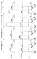
図2は、本発明の第1実施形態に係わるプラズマ処理シーケンスを従来例と比較して示す図である。なお、‘EPD’はエンドポイントディテクタ17による終点検出、‘TopRF’は上部電極2へのRFパワーの印加、‘BottomRF’はサセプタ3へのRFパワーの印加、‘HV’は静電チャック6のオンオフ、‘BackHe’はウエハW裏面へのHeガスの導入をそれぞれ示している。
【0034】
図2(a)において、プラズマ処理を行う場合、ウエハWをサセプタ3上に載置する。そして、処理室1内を排気し、処理室1内の圧力を調節しつつ、エッチングガスを処理室1内に導入する。
【0035】
次に、高周波電源11からのRFパワーを上部電極2に印加した後(t2)、高周波電源12からのRFパワーをサセプタ3に印加することにより(t3)、エッチングガスをプラズマ化するとともに、ウェハWに入射するイオンエネルギーを制御する。それと同時に、高圧直流電源13(HV)をオンして、ウエハWを静電チャック6により固定するとともに、開閉バルブ14aを開いて、Heガス14(Back He)をウエハW裏面に噴出させ、ウエハWの温度を制御する。ここで、RFパワーを上部電極2に印加した後、RFパワーがサセプタ3に印加するとともに、高圧直流電源13をオンすることにより、プラズマのない状態で高圧直流電圧が静電チャック6に印加されることを防止することができ、ウエハW表面へのパーティクルの吸着を抑制することができる。
【0036】
次に、エンドポイントディテクタ17(EPD)がエッチングの終点を検出すると(t5)、高周波電源12からのRFパワー(Bottom RF)をオフするとともに(t5)、ウエハW裏面へのHeガス14の供給を停止する(t5)。また、エッチングが進行せず、かつ、プラズマ放電を維持可能な範囲、例えば、200W以下に、高周波電源11からのRFパワー(Top RF)を制御する(t5)。
【0037】
なお、終点の検出方法は、エンドポイントディテクタ17を用いる方法以外にも、エッチング時間の計測結果に基づいて終点を検出するようにしてもよい。
【0038】
これにより、ウエハWが静電チャック6から脱離可能となる前に、ウエハW裏面へのHeガス14の供給が停止されるので、Heガス14の圧力によりウエハWが吹き飛ぶことを防止できる。
【0039】
次に、高圧直流電源13をオフして、ウエハWを静電チャック6から脱離可能にする(t6)。そして、高周波電源11からのRFパワーをオフし、プラズマ放電を停止させる(t7)。
【0040】
これにより、高周波電源11からのRFパワーをオフする際には、プラズマ放電が維持されているので、ウェハへのパーティクルの吸着を抑制することが可能となる。また、この時のプラズマ放電は、エッチングが進行しないパワーに制御されているので、エンドポイントディテクタ17による終点検出後に、プラズマ放電を維持した場合においても、エッチングの進行を抑制できる。
【0041】
なお、ウエハW裏面へのHeガス14の供給を停止した時に、開閉バルブ15を開いて、ウエハWの裏面の真空引きを行うようにしてもよい。これにより、ウエハWの裏面の圧力を処理室1内の圧力と一致させることができ、ウェハチャッキングミスをより完全に防止することができる。
【0042】
一方、図2(b)に示すように、高圧直流電源13をオンした後に、RFパワーをオンすると、プラズマがない状態で、ウェハWにクローン力がかかり、エッチング開始時におけるウェハWへのパーティクルの吸着が増加する。また、エンドポイントディテクタ17(EPD)が終点を検出した時に(t5)、高周波電源12からのRFパワーをオフすると同時に、高周波電源11からのRFパワーをオフすると、プラズマがない状態で、ウェハWにクローン力がかかる。このため、エッチング終了時においても、ウェハWへのパーティクルの吸着が増加する。
【0043】
例えば、実験例として、シリコン酸化膜、多結晶シリコン膜および反射防止膜が積層されたサンプル上に、開口部がパターニングされたフォトレジスト膜をマスクとしてエッチングを行った後、パターン欠陥検査装置でウエハW上の欠陥の個数を数えた。
【0044】
図3は、この実験例におけるプラズマ処理シーケンスを示す図である。図3において、反射防止膜のエッチング条件として、Cl系混合ガスを用い、ウエハW裏面におけるHe圧力を3Torrにした。また、上部電極2のRFパワーを300Wにし、その0.5秒後に、静電チャック6をオンすると同時に、サセプタ3のRFパワーを30Wにしてエッチングを行った後、サセプタ3のRFパワーをオフすると同時に、上部電極2のRFパワーを200Wに低下させ、その3秒後に静電チャック6をオフし、そのさらに1秒後に上部電極2のRFパワーをオフした。
【0045】
また、多結晶シリコン膜表面上の自然酸化膜のエッチング条件として、Cl2系ガスを用いた。また、上部電極2のRFパワーを225Wにし、その0.5秒後に、静電チャック6をオンすると同時に、サセプタ3のRFパワーを200Wにしてエッチングを行った後、サセプタ3のRFパワーをオフにし、その3秒後に静電チャック6をオフし、そのさらに1秒後に上部電極2のRFパワーをオフした。
【0046】
また、多結晶シリコン膜のメインエッチング条件として、Cl2系混合ガスを用いた。また、上部電極2のRFパワーを635Wにし、その0.5秒後に、静電チャック6をオンすると同時に、サセプタ3のRFパワーを150Wにしてエッチングを行った後、サセプタ3のRFパワーをオフすると同時に、上部電極2のRFパワーを200Wに低下させ、その3秒後に静電チャック6をオフし、そのさらに1秒後に上部電極2のRFパワーをオフした。
【0047】
また、多結晶シリコン膜のオーバーエッチング条件として、HBr混合ガスを用いた。また、上部電極2のRFパワーを375Wにし、その0.5秒後に、静電チャック6をオンすると同時に、サセプタ3のRFパワーを50Wにしてエッチングを行った後、サセプタ3のRFパワーをオフすると同時に、上部電極2のRFパワーを200Wに低下させ、その3秒後に静電チャック6をオフし、そのさらに1秒後に上部電極2のRFパワーをオフした。
【0048】
この結果、処理2枚目のウェハWにおいて、図2(a)のシーケンスでは、図2(b)のシーケンスに対し、欠陥の個数が5.3%に低下した。また、処理13枚目のウェハWにおいて、図2(a)のシーケンスでは、図2(b)のシーケンスに対し、欠陥の個数が8.6%に低下した。また、処理24枚目のウェハWにおいて、図2(a)のシーケンスでは、図2(b)のシーケンスに対し、欠陥の個数が4.5%に低下した。
【0049】
なお、上述した実施形態では、上下電極印加RIE装置を例にとって説明したが、エッチング装置以外に適用してもよく、例えば、プラズマCVD装置などでもよい。これにより、膜厚を正確に制御しつつ、パーティクルの吸着を抑制することが可能となる。
【0050】
また、マグネトロンプラズマ処理装置、ECR(電子サイクロトロン共鳴)プラズマ処理装置、HEP(ヘリコン波励起プラズマ)処理装置、ICP(誘導結合プラズマ)処理装置、TCP(転送結合プラズマ)処理装置などに適用するようにしてもよい。
【0051】
図4は、本発明の第2〜4実施形態に係わるプラズマ処理シーケンスを示す図である。なお、上述した図2(a)の実施形態では、エンドポイントディテクタ17が終点を検出した時に(t5)、高周波電源12からのRFパワーをオフすると同時に、エッチングが進行せず、かつ、プラズマ放電を維持可能な範囲に、高周波電源11からのRFパワーを制御した。これに対し、図4(a)の実施形態では、エンドポイントディテクタ17が終点を検出した時に(t5)、高周波電源11からのRFパワーをオフすると同時に、エッチングが進行せず、かつ、プラズマ放電を維持可能な範囲に、高周波電源12からのRFパワーを制御する。
【0052】
これにより、ウェハWに入射するイオンエネルギーを制御しつつ、エッチングが進行しないようにプラズマ放電を維持することができ、パーティクルの吸着を抑制することが可能となるとともに、チャージアップダメージを低減することができる。
【0053】
また、図4(b)の実施形態では、エンドポイントディテクタ17が終点を検出した時に(t5)、高周波電源11、12のRFパワーのいずれもオフすることなく、エッチングが進行せず、かつ、プラズマ放電を維持可能な範囲に、高周波電源11、12のRFパワーを制御する。そして、高圧直流電源13をオフして、静電チャック6からウエハWを脱離可能にする(t6)。その後、高周波電源11からのRFパワーをオフした後(t7)、高周波電源12からのRFパワーをオフする(t8)。
【0054】
これにより、プラズマ密度およびイオンエネルギーの双方を制御しつつ、プラズマ処理が進行しない範囲でプラズマ放電を維持することができ、パーティクルの付着やオーバーエッチングの発生をより改善することが可能となるとともに、チャージアップダメージを低減することができる。
【0055】
また、図4(c)の実施形態では、エンドポイントディテクタ17が終点を検出した時に(t5)、高周波電源12のRFパワーを低下させることなくそのまま維持するとともに、エッチングが進行せず、かつ、プラズマ放電を維持可能な範囲に、高周波電源11のRFパワーを制御する。そして、高圧直流電源13をオフして、静電チャック6からウエハWを脱離可能にする(t6)。その後、高周波電源11からのRFパワーをオフした後(t7)、高周波電源12からのRFパワーをオフする(t8)。
【0056】
これによっても、イオンエネルギーの制御が行われない状態で、プラズマ放電が維持されることを防止することができ、チャージアップダメージを低減することができる。
【0057】
図5は、本発明の第5実施形態に係わるプラズマ処理シーケンスを従来例と比較して示す図である。なお、上述した第1実施形態はRFパワーの印加の開始方法および終了方法に関するもの、第2〜第4実施形態はRFパワーの印加の終了方法に関するのであるのに対し、この第5実施形態はRFパワーの印加の開始方法に関するものである。
【0058】
図5(b)において、従来の方法では、ウエハWをサセプタ3上に載置した後、高圧直流電源13をオンして、ウエハWを静電チャック6で固定するとともに(t1)、Heガス14をウエハW裏面に噴出させる(t1)。そして、高周波電源11からのRFパワーをオンした後(t2)、高周波電源12からのRFパワーをオンする(t3)。
【0059】
一方、本実施形態では、図5(a)に示すように、ウエハWを静電チャック6により固定するとともに(t1)、Heガス14をウエハW裏面に噴出させる(t1)。そして、高周波電源12からのRFパワーをオンした後(t2)、高周波電源11からのRFパワーをオンする(t3)。
【0060】
これにより、RFパワーの印加を開始する場合に、イオンエネルギーの制御が行われない状態で、プラズマ放電が開始されることを防止することができ、チャージアップダメージを低減することができる。
【0061】
例えば、実験例として、Cl2系ガスを流量50sccmで用い、上部電極2のRFパワーを525W、サセプタ3のRFパワーを70W、圧力を5mTorr、電極間間隔を115mmとして、シリコン酸化膜上の多結晶シリコン膜のエッチングを行った。この場合、図5(b)のシーケンスでは、シリコン酸化膜絶縁耐圧の不良率が8%だったのに対し、図5(a)のシーケンスでは、シリコン酸化膜絶縁耐圧の不良率が0%だった。
【0062】
なお、図5の実施形態では、高圧直流電源13をオンしてから、高周波電源12からのRFパワーをオンし、さらに、高周波電源11からのRFパワーをオンする方法について説明したが、高周波電源12からのRFパワーをオンし、さらに、高周波電源11からのRFパワーをオンしてから、高圧直流電源13をオンしてもよい。これにより、RFパワーの印加を開始する段階においても、チャージアップダメージを低減することが可能となるだけでなく、パーティクルの吸着を抑制することも可能となる。
【0063】
また、高圧直流電源13をオンする前に、高周波電源11、12からのRFパワーをオンする場合には、高周波電源11、12からのRFパワーを、その間エッチングが進行せず、かつ、プラズマ放電を維持可能な範囲に制御してもよい。
これにより、パーティクルの吸着を抑制しつつ、所定の条件に達しないうちに、エッチングが進行することを防止することができる。
【0064】
また、図5の実施形態では、高周波電源11、12からのRFパワーをオフする場合、高周波電源11、12からのRFパワーを同時にオフする方法について説明したが、高周波電源11からのRFパワーをオフしてから、高周波電源12からのRFパワーをオフしてもよい。
【0065】
【発明の効果】
以上説明したように、本発明によれば、エッチング量を正確に制御しつつ、パーティクルの吸着を抑制することが可能となる。
【図面の簡単な説明】
【図1】本発明の一実施形態に係わるプラズマ処理装置の概略構成を示す断面図である。
【図2】本発明の第1実施形態に係わるプラズマ処理シーケンスを従来例と比較して示す図である。
【図3】本発明の一実施形態に係わるプラズマ処理シーケンスの実験例を示す図である。
【図4】本発明の第2〜4実施形態に係わるプラズマ処理シーケンスを示す図である。
【図5】本発明の第5実施形態に係わるプラズマ処理シーケンスを従来例と比較して示す図である。
【符号の説明】
1 処理室
1a ガス供給管
1b 排気管
2 上部電極
2a ガス噴出孔
3 サセプタ
6 静電チャック
11、12 高周波電源
13 高圧直流電源
14 Heガス供給源
14a 開閉バルブ
14b、15 流量調整バルブ
16 真空ポンプ
17 エンドポイントディテクタ[0001]
The present invention relatesto a plasma processingequipment, in particular, is suitably applied to a case of applying RF power to the upper and lower electrodes.
[0002]
[Prior art]
Some conventional plasma processing apparatuses use an electrostatic chuck to fix the wafer in the chamber. In this method using an electrostatic chuck, the wafer is fixed by applying a high-voltage DC voltage to the electrostatic chuck and applying a Coulomb force to the wafer. Here, when a high-voltage DC voltage is applied to the electrostatic chuck in the absence of plasma, particles adhere to the wafer surface due to the Coulomb force acting on the wafer. Therefore, at the start of the process, the RF power is turned on and then the high-voltage DC voltage of the electrostatic chuck is turned on. At the end of the process, the high-voltage DC voltage of the electrostatic chuck is turned off and then the RF power is turned off. In this state, high voltage direct current voltage is prevented from being applied to the electrostatic chuck, and adsorption of particles on the wafer surface is reduced.
[0003]
[Problems to be solved by the invention]
However, in this method, since the wafer is exposed to plasma even after the high-voltage DC voltage of the electrostatic chuck is turned off, the etching proceeds more than the desired etching amount, and the finished shape and dimensions are adversely affected. There was a problem that performance deteriorated.
[0004]
An object of the present invention is to accurately control the etching amount, is to providea plasma processingequipment capable of suppressing the adsorption of particles.
[0005]
[Means for Solving the Problems]
In order to solve the above-described problem, according to the first aspect of the present invention, the wafer is plasma-treated by fixing the wafer via the electrostatic chuck and applying high-frequency power to the upper and lower electrodes. A step of maintaining plasma discharge in a range in which the plasma processing does not proceed after completion of the plasma processing, and a step of stopping supply of a cooling gas supplied to the back surface of the wafer via the electrostatic chuck; The step of stopping the application of the DC voltage to the electrostatic chuck and the step of stopping the plasma discharge after stopping the application of the DC voltage,the step of maintaining the plasma discharge comprising the plasma treatment At the end of the process, the application of the high-frequency power to the upper electrode is stopped, and the plasma treatment is performed within the range where the plasma treatment does not proceed. As electricity is maintained, andcontrolling the RF power applied to the lower electrode.
[0006]
Thereby, even when the plasma discharge is maintained after the plasma processing is finished, the plasma processing can be prevented from proceeding. For this reason, even when the application of the DC voltage to the electrostatic chuck is stopped while the plasma discharge is maintained, the etching does not proceed further after the plasma processing is completed, and the adsorption of particles to the wafer is suppressed. However, application of the DC voltage can be stopped.
[0010]
This makes it possible to reduce the frequency at which the plasma discharge is maintained, while maintaining the plasma discharge while controlling the energy of ions incident on the wafer, thereby reducing charge-up damage. it can.
[0011]
According to thesecond aspect of the present invention,the step of fixing the wafer via theelectrostatic chuck, the step of performing plasma processing on the wafer by applying high frequency power to the upper and lower electrodes, After completion, the step of maintaining the plasma discharge in a range where the plasma processing does not proceed, the step of stopping the supply of the cooling gas supplied to the back surface of the wafer via the electrostatic chuck, and the direct current to the electrostatic chuck And a step of stopping the plasma discharge after stopping the application of the DC voltage, and the step of maintaining the plasma dischargeincludes the step of stopping the plasma processing at the end of the plasma processing. The high frequency power applied to the upper and lower electrodes is controlled so that the plasma discharge is maintained within a range in which the plasma does not travel, and the The step of stopping the Zuma discharge, after stopping the application of RF power to the upper electrode, characterized in that stopping the application of RF power to the lower electrode.
[0012]
Thereby, while controlling both the plasma density and the ion energy, it is possible to maintain the plasma discharge in a range where the plasma treatment does not proceed, and it becomes possible to further improve the adhesion of particles and the occurrence of overetching, Charge-up damage can be reduced.
[0013]
According to athird aspect of the present invention,the step of fixing the wafer via anelectrostatic chuck, the step of performing plasma processing on the wafer by applying high frequency power to the upper and lower electrodes, After completion, the step of maintaining the plasma discharge in a range where the plasma processing does not proceed, the step of stopping the supply of the cooling gas supplied to the back surface of the wafer via the electrostatic chuck, and the direct current to the electrostatic chuck a step of stopping the application of voltage, after stopping the application of the DC voltage, and a step of stopping said plasma discharge, the step of maintaining apre-Symbol plasma discharge at the end of the plasma treatment, the lower electrode The high frequency power applied to is maintained as it is, and the plasma discharge is maintained within the range where the plasma treatment does not proceed. The step of controlling the high frequency power applied to the upper electrode and stopping the plasma discharge stops the application of the high frequency power to the lower electrode after stopping the application of the high frequency power to the upper electrode. features and topulp plasma processing apparatus that.
[0014]
Thereby, it is possible to prevent the plasma discharge from being maintained in a state where the ion energy is not controlled, and to reduce the charge-up damage.
[0019]
According to afourth aspect of the present invention, an electrostatic chuck that fixes a wafer on a susceptor, a DC voltage source that applies a DC voltage to the electrostatic chuck, anupper electrode, a lower electrode, and the upper electrode An upper power applying means for applying a high frequency power to the lower electrode, and a lower power applying means for applying a high frequency power to the lower electrode, a plasma generating means for generating plasma inthe chamber, and after the plasma treatment, the plasma treatment Plasma discharge is maintainedin a range in which the plasma discharge does not proceed, andafter stopping the application of the high frequency power to the upper electrode, the plasma discharge control meansfor stopping the application of the high frequency power to the lower electrode, and the plasma discharge is maintained. And a DC voltage stopping means for stopping the application of the DC voltage to the electrostatic chuck.
[0020]
As a result, the plasma discharge can be maintained while suppressing the progress of the plasma processing, and the application of the DC voltage to the electrostatic chuck is stopped while the plasma discharge is maintained in order to suppress the adsorption of particles to the wafer. Even in such a case, the progress of overetching can be suppressed.
[0022]
Thereby, while controlling the ion energy, plasma discharge can be maintained in a range where the plasma processing does not proceed, and adsorption of particles to the wafer can be suppressed without causing charge-up damage.
[0023]
According to afifth aspect of the present invention, there is provided a cooling gas supply means for supplying a cooling gas to the back surface of the wafer via the electrostatic chuck, and a DC voltage applied to the electrostatic chuck after completion of the plasma processing. Cooling gas stop means for stopping the supply of the cooling gas before stopping the application is provided.
[0024]
This makes it possible to reduce the pressure applied to the back surface of the wafer before stopping the chucking of the wafer, thereby preventing a wafer chucking error.
[0025]
DETAILED DESCRIPTION OF THE INVENTION
Hereinafter, a plasma processing apparatus according to an embodiment of the present invention will be described with reference to the drawings.
[0026]
FIG. 1 is a cross-sectional view showing a schematic configuration of a plasma processing apparatus according to an embodiment of the present invention. In FIG. 1, an
[0027]
Here, the
[0028]
The
[0029]
An
[0030]
The
[0031]
The
[0032]
Further, an
[0033]
FIG. 2 is a diagram showing a plasma processing sequence according to the first embodiment of the present invention in comparison with a conventional example. 'EPD' is the end point detection by the
[0034]
In FIG. 2A, when performing plasma processing, the wafer W is placed on the
[0035]
Next, after applying RF power from the high frequency power supply 11 to the upper electrode 2 (t2), applying RF power from the high frequency power supply 12 to the susceptor 3 (t3), the etching gas is turned into plasma, and the wafer is turned on. The ion energy incident on W is controlled. At the same time, the high-voltage DC power supply 13 (HV) is turned on, the wafer W is fixed by the
[0036]
Next, when the end point detector 17 (EPD) detects the end point of etching (t5), the RF power (Bottom RF) from the high frequency power source 12 is turned off (t5) and the He gas 14 is supplied to the back surface of the wafer W. Is stopped (t5). Further, the RF power (Top RF) from the high frequency power supply 11 is controlled within a range in which etching does not proceed and plasma discharge can be maintained, for example, 200 W or less (t5).
[0037]
Note that the end point may be detected based on the measurement result of the etching time in addition to the method using the
[0038]
As a result, the supply of the He gas 14 to the back surface of the wafer W is stopped before the wafer W can be detached from the
[0039]
Next, the high-voltage DC power supply 13 is turned off so that the wafer W can be detached from the electrostatic chuck 6 (t6). Then, the RF power from the high frequency power supply 11 is turned off, and the plasma discharge is stopped (t7).
[0040]
Thereby, when the RF power from the high frequency power supply 11 is turned off, the plasma discharge is maintained, so that the adsorption of particles to the wafer can be suppressed. Further, since the plasma discharge at this time is controlled to a power at which the etching does not proceed, the progress of the etching can be suppressed even when the plasma discharge is maintained after the end point is detected by the
[0041]
When the supply of the He gas 14 to the back surface of the wafer W is stopped, the open /
[0042]
On the other hand, as shown in FIG. 2B, when the RF power is turned on after the high-voltage DC power supply 13 is turned on, the clonal force is applied to the wafer W in the absence of plasma, and the particles applied to the wafer W at the start of etching. Increased adsorption. When the end point detector 17 (EPD) detects the end point (t5), the RF power from the high frequency power source 12 is turned off, and at the same time, the RF power from the high frequency power source 11 is turned off. The clone power is applied. For this reason, even when etching is completed, the adsorption of particles to the wafer W increases.
[0043]
For example, as an experimental example, after etching a sample in which a silicon oxide film, a polycrystalline silicon film, and an antireflection film are stacked using a photoresist film with a patterned opening as a mask, the wafer is used with a pattern defect inspection apparatus. The number of defects on W was counted.
[0044]
FIG. 3 is a diagram showing a plasma processing sequence in this experimental example. In FIG. 3, as the etching conditions for the antireflection film, a Cl-based mixed gas was used, and the He pressure on the back surface of the wafer W was set to 3 Torr. Further, the RF power of the
[0045]
In addition, a Cl2 gas was used as an etching condition for the natural oxide film on the surface of the polycrystalline silicon film. Further, the RF power of the
[0046]
A Cl2 mixed gas was used as the main etching condition for the polycrystalline silicon film. Further, the RF power of the
[0047]
Further, an HBr mixed gas was used as an overetching condition for the polycrystalline silicon film. Further, the RF power of the
[0048]
As a result, in the second wafer W to be processed, the number of defects was reduced to 5.3% in the sequence of FIG. 2A compared to the sequence of FIG. Further, in the 13th wafer W to be processed, in the sequence of FIG. 2A, the number of defects decreased to 8.6% compared to the sequence of FIG. Further, in the 24th wafer W processed, in the sequence of FIG. 2A, the number of defects decreased to 4.5% as compared to the sequence of FIG.
[0049]
In the above-described embodiment, the upper and lower electrode application RIE apparatus has been described as an example. However, the present invention may be applied to an apparatus other than an etching apparatus, for example, a plasma CVD apparatus. This makes it possible to suppress the adsorption of particles while accurately controlling the film thickness.
[0050]
Also, it is applied to a magnetron plasma processing apparatus, an ECR (electron cyclotron resonance) plasma processing apparatus, a HEP (helicon wave excitation plasma) processing apparatus, an ICP (inductively coupled plasma) processing apparatus, a TCP (transfer coupled plasma) processing apparatus, and the like. May be.
[0051]
FIG. 4 is a diagram showing a plasma processing sequence according to the second to fourth embodiments of the present invention. In the embodiment of FIG. 2A described above, when the
[0052]
Thereby, while controlling the ion energy incident on the wafer W, it is possible to maintain the plasma discharge so that the etching does not proceed, and it becomes possible to suppress the adsorption of particles and reduce the charge-up damage. Can do.
[0053]
In the embodiment of FIG. 4B, when the
[0054]
Thereby, while controlling both the plasma density and the ion energy, it is possible to maintain the plasma discharge in a range where the plasma treatment does not proceed, and it becomes possible to further improve the adhesion of particles and the occurrence of overetching, Charge-up damage can be reduced.
[0055]
Further, in the embodiment of FIG. 4C, when the
[0056]
Also by this, it is possible to prevent the plasma discharge from being maintained in a state where the ion energy is not controlled, and to reduce the charge-up damage.
[0057]
FIG. 5 is a diagram showing a plasma processing sequence according to the fifth embodiment of the present invention in comparison with a conventional example. The first embodiment described above relates to the RF power application start method and the end method, and the second to fourth embodiments relate to the RF power application end method, whereas the fifth embodiment The present invention relates to a method for starting application of RF power.
[0058]
5B, in the conventional method, after the wafer W is placed on the
[0059]
On the other hand, in the present embodiment, as shown in FIG. 5A, the wafer W is fixed by the electrostatic chuck 6 (t1), and the He gas 14 is ejected to the back surface of the wafer W (t1). Then, after the RF power from the high frequency power supply 12 is turned on (t2), the RF power from the high frequency power supply 11 is turned on (t3).
[0060]
Thereby, when application of RF power is started, plasma discharge can be prevented from being started in a state where ion energy is not controlled, and charge-up damage can be reduced.
[0061]
For example, as an experimental example, a Cl2 gas is used at a flow rate of 50 sccm, the RF power of the
[0062]
In the embodiment of FIG. 5, the method of turning on the RF power from the high-frequency power source 12 after turning on the high-voltage DC power source 13 and then turning on the RF power from the high-frequency power source 11 has been described. The high-voltage DC power supply 13 may be turned on after the RF power from 12 is turned on and the RF power from the high-frequency power supply 11 is turned on. Thereby, even at the stage where the application of RF power is started, not only charge-up damage can be reduced, but also adsorption of particles can be suppressed.
[0063]
Further, when the RF power from the high frequency power supplies 11 and 12 is turned on before the high voltage DC power supply 13 is turned on, the RF power from the high frequency power supplies 11 and 12 is not etched during that time, and plasma discharge is performed. May be controlled within a range that can be maintained.
Thereby, it is possible to prevent the etching from progressing before the predetermined condition is reached while suppressing the adsorption of particles.
[0064]
In the embodiment of FIG. 5, the method of simultaneously turning off the RF power from the high frequency power supplies 11 and 12 when turning off the RF power from the high frequency power supplies 11 and 12 has been described. After turning off, the RF power from the high frequency power supply 12 may be turned off.
[0065]
【The invention's effect】
As described above, according to the present invention, it is possible to suppress the adsorption of particles while accurately controlling the etching amount.
[Brief description of the drawings]
FIG. 1 is a cross-sectional view showing a schematic configuration of a plasma processing apparatus according to an embodiment of the present invention.
FIG. 2 is a diagram showing a plasma processing sequence according to the first embodiment of the present invention in comparison with a conventional example.
FIG. 3 is a diagram showing an experimental example of a plasma processing sequence according to an embodiment of the present invention.
FIG. 4 is a view showing a plasma processing sequence according to second to fourth embodiments of the present invention.
FIG. 5 is a diagram showing a plasma processing sequence according to a fifth embodiment of the present invention in comparison with a conventional example.
[Explanation of symbols]
DESCRIPTION OF
Claims (5)
Translated fromJapanese上下電極に高周波電力を印加することにより、前記ウエハのプラズマ処理を行うステップと、
前記プラズマ処理の終了後に、前記プラズマ処理が進行しない範囲でプラズマ放電を維持するステップと、
前記静電チャックを介してウエハの裏面に供給される冷却ガスの供給を停止するステップと、
前記静電チャックへの直流電圧の印加を停止するステップと、
前記直流電圧の印加を停止させた後に、前記プラズマ放電を停止させるステップとを備え、
前記プラズマ放電を維持するステップは、前記プラズマ処理の終了時に、上部電極への高周波電力の印加を停止させるとともに、前記プラズマ処理が進行しない範囲でプラズマ放電が維持されるように、下部電極へ印加される高周波電力を制御する
ことを特徴とするプラズマ処理装置。Fixing the wafer via an electrostatic chuck;
Performing plasma treatment of the wafer by applying high frequency power to the upper and lower electrodes;
Maintaining the plasma discharge in a range in which the plasma treatment does not proceed after the plasma treatment is completed;
Stopping the supply of cooling gas supplied to the back surface of the wafer via the electrostatic chuck;
Stopping application of a DC voltage to the electrostatic chuck;
Stopping the plasma discharge after stopping application of the DC voltage,
The step of maintaining the plasma discharge is applied to the lower electrode so that the application of the high frequency power to the upper electrode is stopped at the end of the plasma processing and the plasma discharge is maintained in a range where the plasma processing does not proceed. A plasma processing apparatusfor controlling high frequency power to be generated .
上下電極に高周波電力を印加することにより、前記ウエハのプラズマ処理を行うステップと、
前記プラズマ処理の終了後に、前記プラズマ処理が進行しない範囲でプラズマ放電を維持するステップと、
前記静電チャックを介してウエハの裏面に供給される冷却ガスの供給を停止するステップと、
前記静電チャックへの直流電圧の印加を停止するステップと、
前記直流電圧の印加を停止させた後に、前記プラズマ放電を停止させるステップとを備え、
前記プラズマ放電を維持するステップは、前記プラズマ処理の終了時に、前記プラズマ処理が進行しない範囲でプラズマ放電が維持されるように、前記上下電極へ印加される高周波電力を制御し、前記プラズマ放電を停止させるステップは、上部電極への高周波電力の印加を停止させた後に、下部電極への高周波電力の印加を停止させることを特徴とするプラズマ処理装置。Fixing the wafer via an electrostatic chuck;
Performing plasma treatment of the wafer by applying high frequency power to the upper and lower electrodes;
Maintaining the plasma discharge in a range in which the plasma treatment does not proceed after the plasma treatment is completed;
Stopping the supply of cooling gas supplied to the back surface of the wafer via the electrostatic chuck;
Stopping application of a DC voltage to the electrostatic chuck;
Stopping the plasma discharge after stopping application of the DC voltage,
The step of maintaining the plasma discharge includes controlling the high-frequency power applied to the upper and lower electrodes so that the plasma discharge is maintained within a range in which the plasma processing does not proceed at the end of the plasma processing, step of stopping, after stopping the application of RF power to the upper electrode, wherein the topulp plasma processing apparatus that stops the application of RF power to the lower electrode.
上下電極に高周波電力を印加することにより、前記ウエハのプラズマ処理を行うステップと、
前記プラズマ処理の終了後に、前記プラズマ処理が進行しない範囲でプラズマ放電を維持するステップと、
前記静電チャックを介してウエハの裏面に供給される冷却ガスの供給を停止するステップと、
前記静電チャックへの直流電圧の印加を停止するステップと、
前記直流電圧の印加を停止させた後に、前記プラズマ放電を停止させるステップとを備え、
前記プラズマ放電を維持するステップは、前記プラズマ処理の終了時に、下部電極へ印加される高周波電力をそのまま維持するとともに、前記プラズマ処理が進行しない範囲でプラズマ放電が維持されるように、上部電極へ印加される高周波電力を制御し、前記プラズマ放電を停止させるステップは、前記上部電極への高周波電力の印加を停止させた後に、前記下部電極への高周波電力の印加を停止させることを特徴とするプラズマ処理装置。Fixing the wafer via an electrostatic chuck;
Performing plasma treatment of the wafer by applying high frequency power to the upper and lower electrodes;
Maintaining the plasma discharge in a range in which the plasma treatment does not proceed after the plasma treatment is completed;
Stopping the supply of cooling gas supplied to the back surface of the wafer via the electrostatic chuck;
Stopping application of a DC voltage to the electrostatic chuck;
Stopping the plasma discharge after stopping application of the DC voltage,
Maintaining apre-Symbol plasma discharge, the at the end of the plasma treatment, as well as maintain the RF power applied to the lower electrode, plasma discharge is maintained in the range of the plasma processing does not proceed, the upper electrode The step of controlling the high-frequency power applied to and stopping the plasma discharge stops the application of the high-frequency power to the lower electrode after stopping the application of the high-frequency power to the upper electrode. toHelp plasma processing apparatus.
前記静電チャックに直流電圧を印加する直流電圧源と、
上部電極と、下部電極と、前記上部電極に高周波電力を印加する上部電力印加手段と、前記下部電極に高周波電力を印加する下部電力印加手段とを備え、チャンバ内にプラズマを発生させるプラズマ発生手段と、
プラズマ処理の終了後に、前記プラズマ処理が進行しない範囲でプラズマ放電を維持し、前記上部電極への高周波電力の印加を停止させた後、前記下部電極への高周波電力の印加を停止させるプラズマ放電制御手段と、
前記プラズマ放電が維持されている間に、前記静電チャックへの直流電圧の印加を停止する直流電圧停止手段と
を備えることを特徴とするプラズマ処理装置。An electrostatic chuck for fixing the wafer on the susceptor;
A DC voltage source for applying a DC voltage to the electrostatic chuck;
Plasma generating means for generating plasma ina chamber, comprising an upper electrode, a lower electrode, upper power applying means for applying high frequency power to the upper electrode, and lower power applying means for applying high frequency power to the lower electrode When,
After the plasma treatment is finished, plasma discharge is maintainedin a range where the plasma treatment does not proceed, andafter stopping the application of the high-frequency power to the upper electrode, the plasma discharge controlfor stopping the application of the high-frequency power to the lower electrode Means,
A plasma processing apparatus comprising: a DC voltage stopping unit that stops application of a DC voltage to the electrostatic chuck while the plasma discharge is maintained.
Priority Applications (5)
| Application Number | Priority Date | Filing Date | Title |
|---|---|---|---|
| JP2001062284AJP4657473B2 (en) | 2001-03-06 | 2001-03-06 | Plasma processing equipment |
| US10/469,235US20040076762A1 (en) | 2001-03-06 | 2002-03-05 | Plasma processor and plasma processing method |
| PCT/JP2002/002007WO2002071462A1 (en) | 2001-03-06 | 2002-03-05 | Plasma processor and plasma processing method |
| KR1020037011624AKR100886981B1 (en) | 2001-03-06 | 2002-03-05 | Plasma processing apparatus and plasma processing method |
| US11/711,769US7504040B2 (en) | 2001-03-06 | 2007-02-28 | Plasma processing apparatus and plasma processing method |
Applications Claiming Priority (1)
| Application Number | Priority Date | Filing Date | Title |
|---|---|---|---|
| JP2001062284AJP4657473B2 (en) | 2001-03-06 | 2001-03-06 | Plasma processing equipment |
Publications (2)
| Publication Number | Publication Date |
|---|---|
| JP2002270576A JP2002270576A (en) | 2002-09-20 |
| JP4657473B2true JP4657473B2 (en) | 2011-03-23 |
Family
ID=18921445
Family Applications (1)
| Application Number | Title | Priority Date | Filing Date |
|---|---|---|---|
| JP2001062284AExpired - Fee RelatedJP4657473B2 (en) | 2001-03-06 | 2001-03-06 | Plasma processing equipment |
Country Status (4)
| Country | Link |
|---|---|
| US (2) | US20040076762A1 (en) |
| JP (1) | JP4657473B2 (en) |
| KR (1) | KR100886981B1 (en) |
| WO (1) | WO2002071462A1 (en) |
Families Citing this family (72)
| Publication number | Priority date | Publication date | Assignee | Title |
|---|---|---|---|---|
| JP2003234331A (en)* | 2001-12-05 | 2003-08-22 | Tokyo Electron Ltd | Plasma etching method and plasma etching apparatus |
| US7569154B2 (en)* | 2002-03-19 | 2009-08-04 | Tokyo Electron Limited | Plasma processing method, plasma processing apparatus and computer storage medium |
| US7541283B2 (en)* | 2002-08-30 | 2009-06-02 | Tokyo Electron Limited | Plasma processing method and plasma processing apparatus |
| DK1828434T3 (en)* | 2004-09-16 | 2008-03-10 | Kolektor Group Doo | Process for improving the electrical connection properties of the surface of a product made of a polymer-matrix composite |
| US20080053817A1 (en)* | 2006-09-04 | 2008-03-06 | Tokyo Electron Limited | Plasma processing apparatus and plasma processing method |
| DE102011004581A1 (en) | 2011-02-23 | 2012-08-23 | Globalfoundries Dresden Module One Limited Liability Company & Co. Kg | A technique for reducing plasma-induced etch damage during the fabrication of vias in inter-layer dielectrics by modified RF power ramp-up |
| US10537013B2 (en)* | 2012-04-23 | 2020-01-14 | Applied Materials, Inc. | Distributed electro-static chuck cooling |
| US9132436B2 (en) | 2012-09-21 | 2015-09-15 | Applied Materials, Inc. | Chemical control features in wafer process equipment |
| US10256079B2 (en) | 2013-02-08 | 2019-04-09 | Applied Materials, Inc. | Semiconductor processing systems having multiple plasma configurations |
| US9362130B2 (en) | 2013-03-01 | 2016-06-07 | Applied Materials, Inc. | Enhanced etching processes using remote plasma sources |
| US9309598B2 (en) | 2014-05-28 | 2016-04-12 | Applied Materials, Inc. | Oxide and metal removal |
| JP6357436B2 (en) | 2014-07-25 | 2018-07-11 | 株式会社日立ハイテクノロジーズ | Plasma processing equipment |
| US9355922B2 (en) | 2014-10-14 | 2016-05-31 | Applied Materials, Inc. | Systems and methods for internal surface conditioning in plasma processing equipment |
| US9966240B2 (en) | 2014-10-14 | 2018-05-08 | Applied Materials, Inc. | Systems and methods for internal surface conditioning assessment in plasma processing equipment |
| US11637002B2 (en) | 2014-11-26 | 2023-04-25 | Applied Materials, Inc. | Methods and systems to enhance process uniformity |
| US10573496B2 (en) | 2014-12-09 | 2020-02-25 | Applied Materials, Inc. | Direct outlet toroidal plasma source |
| US20160225652A1 (en) | 2015-02-03 | 2016-08-04 | Applied Materials, Inc. | Low temperature chuck for plasma processing systems |
| US9728437B2 (en) | 2015-02-03 | 2017-08-08 | Applied Materials, Inc. | High temperature chuck for plasma processing systems |
| US9741593B2 (en) | 2015-08-06 | 2017-08-22 | Applied Materials, Inc. | Thermal management systems and methods for wafer processing systems |
| US9691645B2 (en) | 2015-08-06 | 2017-06-27 | Applied Materials, Inc. | Bolted wafer chuck thermal management systems and methods for wafer processing systems |
| US9349605B1 (en) | 2015-08-07 | 2016-05-24 | Applied Materials, Inc. | Oxide etch selectivity systems and methods |
| US10504700B2 (en) | 2015-08-27 | 2019-12-10 | Applied Materials, Inc. | Plasma etching systems and methods with secondary plasma injection |
| US10522371B2 (en) | 2016-05-19 | 2019-12-31 | Applied Materials, Inc. | Systems and methods for improved semiconductor etching and component protection |
| US10504754B2 (en) | 2016-05-19 | 2019-12-10 | Applied Materials, Inc. | Systems and methods for improved semiconductor etching and component protection |
| US9865484B1 (en)* | 2016-06-29 | 2018-01-09 | Applied Materials, Inc. | Selective etch using material modification and RF pulsing |
| JP6727068B2 (en) | 2016-08-08 | 2020-07-22 | 株式会社日立ハイテク | Plasma processing apparatus and plasma processing method |
| US10629473B2 (en) | 2016-09-09 | 2020-04-21 | Applied Materials, Inc. | Footing removal for nitride spacer |
| US10546729B2 (en) | 2016-10-04 | 2020-01-28 | Applied Materials, Inc. | Dual-channel showerhead with improved profile |
| US9934942B1 (en) | 2016-10-04 | 2018-04-03 | Applied Materials, Inc. | Chamber with flow-through source |
| US10163696B2 (en) | 2016-11-11 | 2018-12-25 | Applied Materials, Inc. | Selective cobalt removal for bottom up gapfill |
| US10026621B2 (en) | 2016-11-14 | 2018-07-17 | Applied Materials, Inc. | SiN spacer profile patterning |
| US10566206B2 (en) | 2016-12-27 | 2020-02-18 | Applied Materials, Inc. | Systems and methods for anisotropic material breakthrough |
| US10431429B2 (en) | 2017-02-03 | 2019-10-01 | Applied Materials, Inc. | Systems and methods for radial and azimuthal control of plasma uniformity |
| US10319739B2 (en) | 2017-02-08 | 2019-06-11 | Applied Materials, Inc. | Accommodating imperfectly aligned memory holes |
| US10943834B2 (en) | 2017-03-13 | 2021-03-09 | Applied Materials, Inc. | Replacement contact process |
| US11276559B2 (en) | 2017-05-17 | 2022-03-15 | Applied Materials, Inc. | Semiconductor processing chamber for multiple precursor flow |
| JP7176860B6 (en) | 2017-05-17 | 2022-12-16 | アプライド マテリアルズ インコーポレイテッド | Semiconductor processing chamber to improve precursor flow |
| US11276590B2 (en) | 2017-05-17 | 2022-03-15 | Applied Materials, Inc. | Multi-zone semiconductor substrate supports |
| US10497579B2 (en) | 2017-05-31 | 2019-12-03 | Applied Materials, Inc. | Water-free etching methods |
| US10920320B2 (en) | 2017-06-16 | 2021-02-16 | Applied Materials, Inc. | Plasma health determination in semiconductor substrate processing reactors |
| US10541246B2 (en) | 2017-06-26 | 2020-01-21 | Applied Materials, Inc. | 3D flash memory cells which discourage cross-cell electrical tunneling |
| US10727080B2 (en) | 2017-07-07 | 2020-07-28 | Applied Materials, Inc. | Tantalum-containing material removal |
| US10541184B2 (en) | 2017-07-11 | 2020-01-21 | Applied Materials, Inc. | Optical emission spectroscopic techniques for monitoring etching |
| US10043674B1 (en) | 2017-08-04 | 2018-08-07 | Applied Materials, Inc. | Germanium etching systems and methods |
| US10297458B2 (en) | 2017-08-07 | 2019-05-21 | Applied Materials, Inc. | Process window widening using coated parts in plasma etch processes |
| US10903054B2 (en) | 2017-12-19 | 2021-01-26 | Applied Materials, Inc. | Multi-zone gas distribution systems and methods |
| US11328909B2 (en) | 2017-12-22 | 2022-05-10 | Applied Materials, Inc. | Chamber conditioning and removal processes |
| US10854426B2 (en) | 2018-01-08 | 2020-12-01 | Applied Materials, Inc. | Metal recess for semiconductor structures |
| US10964512B2 (en) | 2018-02-15 | 2021-03-30 | Applied Materials, Inc. | Semiconductor processing chamber multistage mixing apparatus and methods |
| US10679870B2 (en) | 2018-02-15 | 2020-06-09 | Applied Materials, Inc. | Semiconductor processing chamber multistage mixing apparatus |
| TWI766433B (en) | 2018-02-28 | 2022-06-01 | 美商應用材料股份有限公司 | Systems and methods to form airgaps |
| US10593560B2 (en) | 2018-03-01 | 2020-03-17 | Applied Materials, Inc. | Magnetic induction plasma source for semiconductor processes and equipment |
| US10319600B1 (en) | 2018-03-12 | 2019-06-11 | Applied Materials, Inc. | Thermal silicon etch |
| US10497573B2 (en) | 2018-03-13 | 2019-12-03 | Applied Materials, Inc. | Selective atomic layer etching of semiconductor materials |
| US10573527B2 (en) | 2018-04-06 | 2020-02-25 | Applied Materials, Inc. | Gas-phase selective etching systems and methods |
| US10490406B2 (en) | 2018-04-10 | 2019-11-26 | Appled Materials, Inc. | Systems and methods for material breakthrough |
| US10699879B2 (en) | 2018-04-17 | 2020-06-30 | Applied Materials, Inc. | Two piece electrode assembly with gap for plasma control |
| US10886137B2 (en) | 2018-04-30 | 2021-01-05 | Applied Materials, Inc. | Selective nitride removal |
| US10872778B2 (en) | 2018-07-06 | 2020-12-22 | Applied Materials, Inc. | Systems and methods utilizing solid-phase etchants |
| US10755941B2 (en) | 2018-07-06 | 2020-08-25 | Applied Materials, Inc. | Self-limiting selective etching systems and methods |
| US10672642B2 (en) | 2018-07-24 | 2020-06-02 | Applied Materials, Inc. | Systems and methods for pedestal configuration |
| US11049755B2 (en) | 2018-09-14 | 2021-06-29 | Applied Materials, Inc. | Semiconductor substrate supports with embedded RF shield |
| US10892198B2 (en) | 2018-09-14 | 2021-01-12 | Applied Materials, Inc. | Systems and methods for improved performance in semiconductor processing |
| US11062887B2 (en) | 2018-09-17 | 2021-07-13 | Applied Materials, Inc. | High temperature RF heater pedestals |
| US11417534B2 (en) | 2018-09-21 | 2022-08-16 | Applied Materials, Inc. | Selective material removal |
| US11682560B2 (en) | 2018-10-11 | 2023-06-20 | Applied Materials, Inc. | Systems and methods for hafnium-containing film removal |
| US11121002B2 (en) | 2018-10-24 | 2021-09-14 | Applied Materials, Inc. | Systems and methods for etching metals and metal derivatives |
| US11437242B2 (en) | 2018-11-27 | 2022-09-06 | Applied Materials, Inc. | Selective removal of silicon-containing materials |
| US11721527B2 (en) | 2019-01-07 | 2023-08-08 | Applied Materials, Inc. | Processing chamber mixing systems |
| US10920319B2 (en) | 2019-01-11 | 2021-02-16 | Applied Materials, Inc. | Ceramic showerheads with conductive electrodes |
| CN111863591A (en)* | 2019-04-28 | 2020-10-30 | 北京北方华创微电子装备有限公司 | A pre-cleaning method |
| CN114999990A (en)* | 2022-06-30 | 2022-09-02 | 北京北方华创微电子装备有限公司 | Control method of semiconductor equipment |
Family Cites Families (25)
| Publication number | Priority date | Publication date | Assignee | Title |
|---|---|---|---|---|
| US4345968A (en)* | 1981-08-27 | 1982-08-24 | Ncr Corporation | End point detection using gas flow |
| JPS59147433A (en)* | 1983-02-14 | 1984-08-23 | Hitachi Ltd | Etching device |
| JPH04207026A (en)* | 1990-11-30 | 1992-07-29 | Toshiba Corp | plasma processing equipment |
| JPH04290225A (en)* | 1991-03-18 | 1992-10-14 | Toshiba Corp | Plasma treatment method |
| US5888414A (en)* | 1991-06-27 | 1999-03-30 | Applied Materials, Inc. | Plasma reactor and processes using RF inductive coupling and scavenger temperature control |
| US5539609A (en)* | 1992-12-02 | 1996-07-23 | Applied Materials, Inc. | Electrostatic chuck usable in high density plasma |
| JP3242166B2 (en)* | 1992-11-19 | 2001-12-25 | 株式会社日立製作所 | Etching equipment |
| KR100290748B1 (en)* | 1993-01-29 | 2001-06-01 | 히가시 데쓰로 | Plasma processing apparatus |
| KR100264445B1 (en)* | 1993-10-04 | 2000-11-01 | 히가시 데쓰로 | Plasma Treatment Equipment |
| JP3257328B2 (en)* | 1995-03-16 | 2002-02-18 | 株式会社日立製作所 | Plasma processing apparatus and plasma processing method |
| US5997962A (en)* | 1995-06-30 | 1999-12-07 | Tokyo Electron Limited | Plasma process utilizing an electrostatic chuck |
| JP2869384B2 (en)* | 1995-06-30 | 1999-03-10 | 東京エレクトロン株式会社 | Plasma processing method |
| KR100226366B1 (en)* | 1995-08-23 | 1999-10-15 | 아끼구사 나오유끼 | Plasma equipment and plasma processing method |
| US5546885A (en)* | 1995-10-12 | 1996-08-20 | Porada; William M. | Collapsible scuba tank supports for an inflatable dinghy |
| US6245202B1 (en)* | 1996-04-12 | 2001-06-12 | Hitachi, Ltd. | Plasma treatment device |
| US5711998A (en)* | 1996-05-31 | 1998-01-27 | Lam Research Corporation | Method of polycrystalline silicon hydrogenation |
| JP3220383B2 (en)* | 1996-07-23 | 2001-10-22 | 東京エレクトロン株式会社 | Plasma processing apparatus and method |
| CN1299226C (en)* | 1997-09-17 | 2007-02-07 | 东京电子株式会社 | System and method for monitoring and controlling gas plasma process |
| US6136165A (en)* | 1997-11-26 | 2000-10-24 | Cvc Products, Inc. | Apparatus for inductively-coupled-plasma-enhanced ionized physical-vapor deposition |
| KR100733241B1 (en) | 1998-11-27 | 2007-06-27 | 동경 엘렉트론 주식회사 | Plasma etching equipment |
| US6277716B1 (en)* | 1999-10-25 | 2001-08-21 | Chartered Semiconductor Manufacturing Ltd. | Method of reduce gate oxide damage by using a multi-step etch process with a predictable premature endpoint system |
| JP3323190B2 (en)* | 2000-04-19 | 2002-09-09 | 松下電器産業株式会社 | Dry etching method, method of manufacturing semiconductor device, and dry etching apparatus |
| JP4559595B2 (en)* | 2000-07-17 | 2010-10-06 | 東京エレクトロン株式会社 | Apparatus for placing object to be processed and plasma processing apparatus |
| JP4129855B2 (en)* | 2001-12-13 | 2008-08-06 | 東京エレクトロン株式会社 | Plasma processing equipment |
| JP2003197615A (en)* | 2001-12-26 | 2003-07-11 | Tokyo Electron Ltd | Plasma treatment apparatus and method for cleaning the same |
- 2001
- 2001-03-06JPJP2001062284Apatent/JP4657473B2/ennot_activeExpired - Fee Related
- 2002
- 2002-03-05KRKR1020037011624Apatent/KR100886981B1/ennot_activeExpired - Fee Related
- 2002-03-05WOPCT/JP2002/002007patent/WO2002071462A1/enactiveApplication Filing
- 2002-03-05USUS10/469,235patent/US20040076762A1/ennot_activeAbandoned
- 2007
- 2007-02-28USUS11/711,769patent/US7504040B2/ennot_activeExpired - Lifetime
Also Published As
| Publication number | Publication date |
|---|---|
| US20070148364A1 (en) | 2007-06-28 |
| US7504040B2 (en) | 2009-03-17 |
| WO2002071462A1 (en) | 2002-09-12 |
| JP2002270576A (en) | 2002-09-20 |
| KR100886981B1 (en) | 2009-03-04 |
| KR20030087634A (en) | 2003-11-14 |
| US20040076762A1 (en) | 2004-04-22 |
Similar Documents
| Publication | Publication Date | Title |
|---|---|---|
| JP4657473B2 (en) | Plasma processing equipment | |
| US8404595B2 (en) | Plasma processing method | |
| KR20210042939A (en) | Equipment and process for electron beam mediated plasma etching and deposition process | |
| US9852922B2 (en) | Plasma processing method | |
| US20140144876A1 (en) | Plasma etching method | |
| US7449414B2 (en) | Method of treating a mask layer prior to performing an etching process | |
| US20040219797A1 (en) | Plasma etching method and plasma etching unit | |
| TW201631656A (en) | Etching method | |
| KR20150104043A (en) | Plasma etching method and plasma etching apparatus | |
| TWI445074B (en) | Method of treating a mask layer prior to rerforming an etching process | |
| JP7433164B2 (en) | Substrate processing system | |
| JP2010140944A (en) | Plasma etching device and plasma cleaning method | |
| JP5064319B2 (en) | Plasma etching method, control program, and computer storage medium | |
| TW200416856A (en) | Method and device for plasma-etching organic material film | |
| US20240047195A1 (en) | Delayed pulsing for plasma processing of wafers | |
| US7572386B2 (en) | Method of treating a mask layer prior to performing an etching process | |
| US7642193B2 (en) | Method of treating a mask layer prior to performing an etching process | |
| US10651077B2 (en) | Etching method | |
| JP2004259819A (en) | Sample surface treatment apparatus and surface treatment method | |
| JPH08195379A (en) | Plasma processing method and plasma processing apparatus | |
| US20200411326A1 (en) | Etching method and substrate processing apparatus | |
| JP3172340B2 (en) | Plasma processing equipment | |
| US20070218691A1 (en) | Plasma etching method, plasma etching apparatus and computer-readable storage medium | |
| JP2003332317A (en) | Resist stripping apparatus and method using plasma | |
| TW202209476A (en) | Method for dry etching silicon carbide films for resist underlayer applications |
Legal Events
| Date | Code | Title | Description |
|---|---|---|---|
| A621 | Written request for application examination | Free format text:JAPANESE INTERMEDIATE CODE: A621 Effective date:20080116 | |
| A131 | Notification of reasons for refusal | Free format text:JAPANESE INTERMEDIATE CODE: A131 Effective date:20100928 | |
| A521 | Request for written amendment filed | Free format text:JAPANESE INTERMEDIATE CODE: A523 Effective date:20101104 | |
| TRDD | Decision of grant or rejection written | ||
| A01 | Written decision to grant a patent or to grant a registration (utility model) | Free format text:JAPANESE INTERMEDIATE CODE: A01 Effective date:20101221 | |
| A01 | Written decision to grant a patent or to grant a registration (utility model) | Free format text:JAPANESE INTERMEDIATE CODE: A01 | |
| A61 | First payment of annual fees (during grant procedure) | Free format text:JAPANESE INTERMEDIATE CODE: A61 Effective date:20101222 | |
| FPAY | Renewal fee payment (event date is renewal date of database) | Free format text:PAYMENT UNTIL: 20140107 Year of fee payment:3 | |
| R150 | Certificate of patent or registration of utility model | Ref document number:4657473 Country of ref document:JP Free format text:JAPANESE INTERMEDIATE CODE: R150 Free format text:JAPANESE INTERMEDIATE CODE: R150 | |
| R250 | Receipt of annual fees | Free format text:JAPANESE INTERMEDIATE CODE: R250 | |
| R250 | Receipt of annual fees | Free format text:JAPANESE INTERMEDIATE CODE: R250 | |
| R250 | Receipt of annual fees | Free format text:JAPANESE INTERMEDIATE CODE: R250 | |
| LAPS | Cancellation because of no payment of annual fees |