JP4656699B2 - Display system - Google Patents
Display systemDownload PDFInfo
- Publication number
- JP4656699B2 JP4656699B2JP2000184302AJP2000184302AJP4656699B2JP 4656699 B2JP4656699 B2JP 4656699B2JP 2000184302 AJP2000184302 AJP 2000184302AJP 2000184302 AJP2000184302 AJP 2000184302AJP 4656699 B2JP4656699 B2JP 4656699B2
- Authority
- JP
- Japan
- Prior art keywords
- display device
- signal format
- edid data
- storage medium
- resolution
- Prior art date
- Legal status (The legal status is an assumption and is not a legal conclusion. Google has not performed a legal analysis and makes no representation as to the accuracy of the status listed.)
- Expired - Fee Related
Links
Images


Landscapes
- Controls And Circuits For Display Device (AREA)
Description
Translated fromJapanese【0001】
【発明の属する技術分野】
本発明は、表示システム、より詳しくは、ホスト装置と表示装置とを変換装置を介して接続された表示システムのプラグアンドプレイによる簡単操作に好適な表示システムに関する。
【0002】
【従来の技術】
近年、コンピュータシステムにおいて、ホスト装置であるコンピュータと、それに接続するための周辺機器の設定が面倒なことから、その設定を簡単にするためのプラグ・アンド・プレイ(Plug and Play)機構を組み込むようになってきた。プラグ・アンド・プレイ機構とは、周辺機器をパソコンに取り付ける(Plug)だけですぐに動く(Play)ようにする機構である。この機構は、プラグ・アンド・プレイ対応のBIOSとプラグ・アンド・プレイ対応のOS(オペレーティングシステム)により実現される。プラグ・アンド・プレイ機構は、例えば、拡張ボードの割り込み(IRQ)、DMAチャネル、およびI/Oアドレスなどのシステムの面倒な設定を自動化したり、パソコンの稼働中に周辺機器を脱着したときに、その周辺機器のデバイス・ドライバを自動的にロード/アンロードすることが可能となる。
【0003】
このようなプラグ・アンド・プレイ機構(機能)を備えた表示装置が製品化されている。表示装置(ディスプレイ)のプラグ・アンド・プレイは、解像度や同期可能な周波数などの表示装置のデータをコンピュータとやり取りすることにより実現している。この表示装置のプラグ・アンド・プレイはVESAにより規格化されたDDC(Display Data Channel)インタフェースにより、表示装置とコンピュータとの通信制御を行い、表示装置の解像度、同期周波数仕様等の情報をEDID(Extended Display Identification Data)として表示装置からコンピュータへ送信し、表示装置の使用範囲を意識した自動設定ができるようになったが、アプリケーションの起動、選択、実行による複雑な操作性を必要としていた。
【0004】
この操作性を改善するものとして、例えば、特開平11−15425号公報に記載の表示装置が挙げられる。この表示装置では、表示装置自体にて解像度、同期周波数の切り替え制御を行い、コンピュータの表示モードを切り替える機能を備え、操作性の向上を図っている。すなわち、コンピュータと表示装置が1対1で接続され、単一の表示装置をコンピュータへ接続する例を示している。
【0005】
【発明が解決しようとする課題】
しかしながら、上記公開公報では、複数の機器を接続して画面を表示する装置に関する記載はない。すなわち、コンピュータと表示装置との間に変換アダプタなどを配置し、この変換アダプタを介してコンピュータと表示装置とを接続すると、プラグ・アンド・プレイが無効になってしまうという問題については考慮されていない。このプラグ・アンド・プレイでは表示装置とコンピュータが直接通信して、データのやり取りを行うことを考慮しているだけで、変換アダプタにより画像信号のフォーマットを変換して表示装置に表示するようなシステムに対しては有効ではない。
【0006】
一方、最近、ウェアラブルコンピュータを小型表示装置(マイクロディスプレイ)と接続し、この小型表示装置を頭部または顔面に装着し、ウェアラブルコンピュータを身につけるようなシステムが開発されている。この装置では専用の表示装置を接続することを想定して開発されたものであるので、種々仕様の小型表示装置を接続するようなことは想定していなかった。従って、この小型表示装置のプラグ・アンド・プレイについても考慮されていなかった。小型表示装置も技術開発が活発になり、汎用的な使用も考慮する必要性が生じてきた。
【0007】
本発明の目的は、このような従来の課題を解決し、複数の装置を接続して表示する表示システムにおいて、プラグ・アンド・プレイを実現し、設定が簡単で適切に装置を使用可能とする表示システムを提供することにある。
【0008】
【課題を解決するための手段】
上記の目的を達成するために、本発明による表示システムは、画像供給装置と、この画像供給装置からの画像信号の伝送方式のみを変換する信号フォーマット変換装置と、この変換された伝送方式の画像信号を表示する表示装置とを有する表示システムにおいて、上記信号フォーマット変換装置と上記表示装置の各々は、各々の性能又は能力を示す各々の入力可能な画像信号の解像度と垂直同期周波数のデータを含むEDIDデータを記録した記憶媒体を備え、上記信号フォーマット変換装置は、上記表示装置の記憶媒体に記録された上記EDIDデータを読み出し、上記信号フォーマット変換装置の記憶媒体に記録された上記EDIDデータと比較し、上記表示装置の記憶媒体に記録された上記EDIDデータに含まれる解像度と垂直同期周波数が上記信号フォーマット変換装置の記憶媒体に記録された上記EDIDデータに含まれる解像度と垂直同期周波数と同等以下の場合は、上記画像供給装置に対して、上記表示装置の記憶媒体に記録された上記EDIDデータに含まれる解像度と垂直同期周波数の画像信号の出力を要求し、上記表示装置の記憶媒体に記録された上記EDIDデータに含まれる解像度と垂直同期周波数が上記信号フォーマット変換装置の記憶媒体に記録された上記EDIDデータに含まれる解像度と垂直同期周波数を上回る場合は、上記画像供給装置に対して、上記信号フォーマット変換装置の記憶媒体に記録された上記EDIDデータに含まれる解像度と垂直同期周波数の画像信号の出力を要求することに特徴がある。
【0012】
上記表示システムにおいて、上記画像供給装置は、上記EDIDデータに基づき、上記信号フォーマット変換装置と上記表示装置の組み合わせが禁止されていることを検出した場合は、上記表示装置への給電を制限するとともに、異常処理を行うことにも特徴がある。
【0013】
上記表示システムにおいて、上記異常処理は、上記表示装置への画像出力を禁止するとともに、上記表示装置以外の表示装置により使用者への警告表示を行うことに特徴がある。
【0014】
上記表示システムにおいて、上記表示装置は、頭部装着型表示装置であることを特徴とする。
【0015】
【発明の実施の形態】
以下、図面を参照して本発明の実施の形態を説明する。
図1から図7は本発明の一実施形態を示したものであり、図1は本発明の第1の実施形態の表示システムを示すブロック構成図、図2は本発明を適用した表示システムの概略ブロック図、図3はEDIDデータの例を示す図、図4はEDIDデータの例を示す図、図5は本発明の第2の実施形態の表示システムを示すブロック構成図、図6は本発明の第3の実施形態の表示システムを示すブロック構成図、図7は本発明の第4の実施形態の表示システムを示すブロック構成図である。
[第1の実施の形態]
本発明の第1の実施の形態を図1〜図4を用いて説明する。
【0016】
ホストPC101には、図2に示すように、信号フォーマット変換器201を介して頭部装着型表示装置301が接続されている。頭部装着型表示装置301としては、例えば、0.47インチのSiチップ・ベースド液晶を用いたものである。フィールドシーケンシャル方式により高精細な画像表示を実現している。この頭部装着型表示装置の詳細については、本出願人が先に提案した特願平11−222855号明細書を参照されたい。
【0017】
画像供給装置としてのホストPCは、標準でTMDSのディジタルインタフェースを有するものや、PCカードスロットにPCカードを形式で提供したタイプのコンピュータが含まれる。また、図示していないが、インタフェースとしては、USBインタフェースやIEEE1394インタフェースを選択的に備えているものとする。
【0018】
図1に示すように、ホストPC101にはTMDSトランスミッタ回路102とDDC制御部103を内蔵しており、TMDSトランスミッタ回路102から画像データと映像タイミング信号が出力される。このときの出力信号フォーマットはTMDSである。一方、頭部装着型表示装置301はGVIFフォーマットの入力信号に対応している。このままでは、ホストPC101に頭部装着型表示装置301を接続できないため、信号フォーマット変換器201が必要になる。この変換器201はTMDSフォーマットのディジタル信号をGVIFフォーマットのディジタルデータに変換する機能を持っている。
【0019】
信号フォーマット変換器201はTMDSレシーバ回路207でホストPC101から送られてくる画像データを受信し、GVIFトランスミッタ回路202で再度ディジタルデータへ変換して頭部装着型表示装置301へ送り出す。
【0020】
EEPROM206には、この変換器201の機能(特徴)を記述したEDIDデータが格納されており、これへの読み書きはCPU204によって行われる。DDC制御部203はCPU204からの指示により、
(1)頭部装着型表示装置301のEDIDデータを読み出す。
(2)ホストPC101に対し装置自体もしくは頭部装着型表示装置301のEDIDデータを書き込む。
(3)異常が発生した場合、その内容をホストPC101に報告し、ホストPC101からの指示を受ける。
【0021】
電源209は信号フォーマット変換器201を経由して頭部装着型表示装置301へ供給される。この経路にはスイッチ208が入っており、CPU204の制御により、電源を部分的にON/OFFできるようになっている。
【0022】
電源209は、ACアダプタ、電池でもよい。但し、少なくとも5V、0.5Aの電力供給が必要である。また、適当なドライバソフトと組み合わせることによりホストPC101のUSBインタフェース、IEEE1394インタフェース、PCIバス、PS/2インタフェースなどから取ってもよい。
【0023】
頭部装着型表示装置301はGVIFレシーバ回路302とLCDドライバ303により、信号フォーマット変換器201から受け取ったGVIFフォーマットのディジタル信号をLCD駆動信号に変換し、LCD304に画像を表示させる。
【0024】
頭部装着型表示装置301のEEPROM308には、この表示装置の機能(特徴)を記述したEDIDデータが格納されており、これへの読み書きはCPU306によって行われる。DDC制御部305はCPU306からの指示により、
(1)信号フォーマット変換器201に対しEDIDデータを書き込む。
(3)異常が発生した場合、その内容を信号フォーマット変換器201に報告し、信号フォーマット変換器201からの指示を受ける。
【0025】
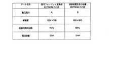
信号フォーマット変換器201のEDIDデータと頭部装着型表示装置301のEDIDデータの例を基に、システムの動作を説明する。図3、図4に示すEDIDデータは一部を示しており、詳細にはVESAの規格を満たす内容のデータを有しているものとする。
【0026】
信号フォーマット変換器201は、頭部装着型表示装置301のEEPROM308に格納された解像度(表示解像度)と垂直同期周波数を読み出す。その結果を、変換器自体の性能と比較して、頭部装着型表示装置301の性能が同等以下の場合(図3)には、ホストPC101に対して頭部装着型表示装置301の能力に応じた出力信号形式を要求する。この例では解像度800×600、垂直同期周波数60Hzを要求する。
【0027】
変換器自体の性能と比較して、頭部装着型表示装置301の性能が上回る場合(図4)には、ホストPC101と頭部装着型表示装置301に対して自体の能力に応じた出力信号形式を要求する。この例では解像度800×600、垂直同期周波数60Hzを要求する。頭部装着型表示装置301へはDDC制御部203、305を通してCPU306に要求が伝えられ、CPU306はLCD304の表示エリアを調節する。
【0028】
こうすることにより、信号フォーマット変換器201と頭部装着型表示装置301の組み合わせにおいて、常に最大の能力を引き出すことができる。
また、図3または図4の製品識別により、信号フォーマット変換器201と頭部装着型表示装置301の組み合わせ使用が禁止されている組み合わせの場合には、信号フォーマット変換器201は、スイッチ208をOFFにして頭部装着型表示装置301の表示部への電力供給を止めるとともに、ホストPC101へ異常処理コードを送る。ホストPC側では異常処理コードに応じた異常処理を行うことにより、画像出力を禁止したり、メインモニタへのエラー表示もしくはLEDの点滅などによる異常表示を行う。この機能により、信号フォーマット変換器201と頭部装着型表示装置301の不正な組み合わせでの使用による電源容量オーバーなどの異常事態を回避することができる。
【0029】
頭部装着型表示装置301は、目の保護のため連続使用の制限を行う場合がある。信号フォーマット変換器201と頭部装着型表示装置301の組み合わせをホストPC101、もしくは信号フォーマット変換器201のCPU204もしくは頭部装着型表示装置301のCPU306で検出し、この組み合わせに応じて制限時間を任意に可変し、目の保護を確実に行うことができる。
【0030】
本発明の第2の実施の形態を図5を用いて説明する。信号フォーマット変換器201は第1の実施形態と同様であるが、頭部装着型表示装置301aはEDIDデータを格納したEEPROM308を有しているが、CPU306、DDC制御部305、RAM307を有していない。
【0031】
信号フォーマット変換器201からの要求に対し、動作モードを変更することはできないが、組み合わせ使用時の判断は信号フォーマット変換器201が行うため、不正な使用の防止は実現できる。CPU306等を持たないため、コスト的に有利であり、機能を簡略化した低価格なシステムを構築できる。
【0032】
本発明の第3の実施の形態を図6を用いて説明する。
信号フォーマット変換器201aはTMDSレシーバ回路207、GVIFトランスミッタ回路202、EDIDデータを格納したEEPROM206、電源209のスイッチングのためのスイッチ208を備えているが、DDC制御部203、CPU204、RAM205を有していない。また、頭部装着型表示装置301aは図5の実施形態と同様であり、DDC制御部305、CPU306、RAM307を有しておらず、EDIDデータを格納したEEPROM308を有している。EEPROM206とEEPROM308はアドレスを変えてあるため、ホストPC101はDDC制御ライン211を通してEEPROM206、308の内容を独立に読み出すことができる。
【0033】
組み合わせの最適化はホストPC101のドライバソフトが行う。また、頭部装着型表示装置301aへの電力供給制限はホストPC101のスイッチ制御部104により信号フォーマット変換器201のスイッチ208を制御するため、不正な使用の防止は実現できる。信号フォーマット変換器201と頭部装着型表示装置301は共にCPU204や306を持たないため、第2の実施形態より更にコスト的に有利である。
【0034】
本発明の第4の実施の形態を図7を用いて説明する。
ホストPC101にはRGB出力部105とDDC制御部103を内蔵しており、RGB出力部105から画像データと映像タイミング信号が出力される。このときの出力フォーマットはアナログRGB形式である。この信号フォーマット変換器はアナログRGBフォーマットのアナログ信号をGVIFフォーマットのディジタルデータに変換する機能を持っている。
【0035】
信号フォーマット変換器201はホストPC101から送られてくる画像データと映像タイミング信号を受信し、ADコンバータ210でディジタルデータへ変換して頭部装着型表示装置301(図1を参照)へ送り出す。
【0036】
ADコンバータ210以外の各部の動作については第1の実施形態と同様であるので、説明を省略する。
上述した実施形態においては、ホストPCと信号フォーマット変換器と表示装置を備えた表示システムにおいて、信号フォーマット変換器自体もプラグ・アンド・プレイ機構を実現しているので、設定が簡単となると同時に、適切な表示装置の使用が可能となる。
【0037】
また、表示装置への電源供給もEDIDデータとして含まれているので、電源供給判断が可能となり、各種の小型表示装置を接続する際にも組合せによる不具合も防止できる。
【0038】
なお、本発明は上述した実施形態に限定されるものではなく、発明の主旨を逸脱しない範囲内において種々の変形や応用が可能であることは勿論である。
【0039】
【発明の効果】
以上説明したように、本発明の表示システムによれば、複数の装置を接続して表示する表示システムにおいて、プラグ・アンド・プレイを実現し、設定が簡単で適切に装置を使用できる。
【図面の簡単な説明】
【図1】本発明の第1の実施形態の表示システムを示すブロック構成図。
【図2】本発明を適用した表示システムの概略ブロック図。
【図3】EDIDデータの例を示す図。
【図4】EDIDデータの例を示す図。
【図5】本発明の第2の実施形態の表示システムを示すブロック構成図。
【図6】本発明の第3の実施形態の表示システムを示すブロック構成図。
【図7】本発明の第4の実施形態の表示システムを示すブロック構成図。
【符号の説明】
101 ホストPC
102 TMDSトランスミッタ回路
103 DDC制御部
104 スイッチ制御部
105 RGB出力部
201、201a、201b 信号フォーマット変換器
202 GVIFトランスミッタ回路
203 DDC制御部
204 CPU
205 RAM
206 EEPROM
207 TMDSレシーバ回路
208 スイッチ
209 電源
210 ADコンバータ
211 DDC制御ライン
301、301a 頭部装着型表示装置
302 GVIFレシーバ回路
303 LCDドライバ
304 LCD
305 DDC制御部
306 CPU
307 RAM
308 EEPROM[0001]
BACKGROUND OF THE INVENTION
The present invention relates to a display system, and more particularly to a display system suitable for simple operation by plug and play of a display system in which a host device and a display device are connected via a conversion device.
[0002]
[Prior art]
In recent years, in a computer system, it is troublesome to set up a computer that is a host device and peripheral devices to be connected to it, so that a plug and play mechanism for simplifying the setting is incorporated. It has become. The plug-and-play mechanism is a mechanism that allows a peripheral device to be moved (Play) just by attaching it to a personal computer (Plug). This mechanism is realized by a plug-and-play compatible BIOS and a plug-and-play compatible OS (operating system). The plug and play mechanism automates troublesome system settings such as expansion board interrupts (IRQ), DMA channels, and I / O addresses, or when a peripheral device is attached or removed while the computer is running The device driver of the peripheral device can be automatically loaded / unloaded.
[0003]
Display devices having such a plug-and-play mechanism (function) have been commercialized. Plug and play of a display device (display) is realized by exchanging data of the display device such as resolution and synchronizable frequency with a computer. The plug and play of this display device performs communication control between the display device and the computer through a DDC (Display Data Channel) interface standardized by VESA, and displays information such as the resolution of the display device and the synchronization frequency specification as EDID ( Extended Display Identification Data) can be sent from the display device to the computer and automatic setting can be made with consideration for the range of use of the display device, but it requires complicated operability by starting, selecting, and executing the application.
[0004]
As a device for improving this operability, for example, a display device described in JP-A-11-15425 can be cited. In this display device, the display device itself has a function of switching the resolution and the synchronization frequency and switching the display mode of the computer, thereby improving operability. That is, an example is shown in which a computer and a display device are connected one-to-one, and a single display device is connected to the computer.
[0005]
[Problems to be solved by the invention]
However, the above publication does not describe an apparatus that displays a screen by connecting a plurality of devices. In other words, if a conversion adapter or the like is placed between the computer and the display device, and the computer and the display device are connected via this conversion adapter, the problem that plug and play becomes invalid is considered. Absent. In this plug-and-play system, a display adapter and a computer communicate directly and exchange data, and a system that converts the format of an image signal using a conversion adapter and displays it on the display device. It is not effective for.
[0006]
On the other hand, recently, a system has been developed in which a wearable computer is connected to a small display device (micro display), the small display device is attached to the head or face, and the wearable computer is worn. Since this device was developed on the assumption that a dedicated display device is connected, it was not assumed that a small display device of various specifications would be connected. Therefore, the plug-and-play of this small display device has not been considered. The technical development of small display devices has become active, and there has been a need to consider general-purpose use.
[0007]
An object of the present invention is to solve such a conventional problem and realize plug and play in a display system in which a plurality of devices are connected and displayed, enabling easy setting and appropriate use of the device. To provide a display system.
[0008]
[Means for Solving the Problems]
In order to achieve the above object, a display system according to the present invention includes an image supply device, a signal format conversion device that convertsonly a transmission method of an image signal from the image supply device, and an image of the converted transmission method. In a display system having a display device for displaying a signal, each of the signal format conversion device and the display device includes data of resolution and vertical synchronization frequency of each inputable image signal indicating the performance or capability of the signal. The signal format conversion device includes a storage medium on which EDID data is recorded, and the signal format conversion device reads the EDID data recorded on the storage medium of the display device and compares it with the EDID data recorded on the storage medium of the signal format conversion device. And the vertical synchronization with the resolution included in the EDID data recorded on the storage medium of the display device. When the wave number is equal to or lower than the resolution and vertical synchronization frequency included in the EDID data recorded on the storage medium of the signal format conversion device, the image number is recorded on the storage medium of the display device. The output of the image signal having the resolution and the vertical synchronization frequency included in the EDID data is requested, and the resolution and the vertical synchronization frequency included in the EDID data recorded on the storage medium of the display device are the storage medium of the signal format conversion device. When the resolution and the vertical synchronization frequency included in the EDID data recorded on the image are higher than the resolution and the vertical synchronization frequency included in the EDID data recorded on the storage medium of the signal format conversion device It is characterized by requiring the output of an image signal with a frequency.
[0012]
In the display system, when theimage supply device detects that the combination of the signal format conversion device and the display device is prohibited based on the EDID data, the image supply device restricts power supply to the display device. Also, there is a featurein performing abnormality processing .
[0013]
In the display system, the abnormality process is characterized inthat image output to the display device is prohibited and a warning isdisplayed to the user by a display device other than the display device.
[0014]
In the display system, the display device isa head-mounted display device.
[0015]
DETAILED DESCRIPTION OF THE INVENTION
Embodiments of the present invention will be described below with reference to the drawings.
FIG. 1 to FIG. 7 show an embodiment of the present invention. FIG. 1 is a block diagram showing a display system according to the first embodiment of the present invention. FIG. 2 shows a display system to which the present invention is applied. FIG. 3 is a schematic block diagram, FIG. 3 is a diagram showing an example of EDID data, FIG. 4 is a diagram showing an example of EDID data, FIG. 5 is a block configuration diagram showing a display system according to a second embodiment of the present invention, and FIG. FIG. 7 is a block diagram illustrating a display system according to a fourth embodiment of the present invention, and FIG. 7 is a block diagram illustrating a display system according to a fourth embodiment of the present invention.
[First Embodiment]
A first embodiment of the present invention will be described with reference to FIGS.
[0016]
As shown in FIG. 2, a head-mounted
[0017]
The host PC as the image supply device includes a standard computer having a TMDS digital interface and a computer of a type in which a PC card is provided in the form of a PC card slot. Although not shown, it is assumed that a USB interface or an IEEE 1394 interface is selectively provided as an interface.
[0018]
As shown in FIG. 1, the
[0019]
The
[0020]
The
(1) Read the EDID data of the head-mounted
(2) Write the EDID data of the device itself or the head mounted
(3) When an abnormality occurs, the contents are reported to the
[0021]
The
[0022]
The
[0023]
The head-mounted
[0024]
EDID data describing the function (feature) of the display device is stored in the
(1) Write EDID data to the
(3) When an abnormality occurs, the content is reported to the
[0025]
Based on the exampleof the EDIDdata of the EDIDdata and the head-mounted
[0026]
The
[0027]
When the performance of the head-mounted
[0028]
By doing so, it is possible to always draw out the maximum capability in the combination of the
3 or 4, if the combination of the
[0029]
The head-mounted
[0030]
A second embodiment of the present invention will be described with reference to FIG. The
[0031]
Although the operation mode cannot be changed in response to a request from the
[0032]
A third embodiment of the present invention will be described with reference to FIG.
The signal format converter 201a includes a
[0033]
The combination optimization is performed by the driver software of the
[0034]
A fourth embodiment of the present invention will be described with reference to FIG.
The
[0035]
The
[0036]
Since the operation of each part other than the
In the above-described embodiment, in the display system including the host PC, the signal format converter, and the display device, the signal format converter itself also realizes the plug and play mechanism. An appropriate display device can be used.
[0037]
In addition, since the power supply to the display device is also included as EDID data, it is possible to determine the power supply, and it is possible to prevent problems due to the combination when various kinds of small display devices are connected.
[0038]
It should be noted that the present invention is not limited to the above-described embodiments, and various modifications and applications can be made without departing from the spirit of the invention.
[0039]
【The invention's effect】
As described above, according to the display system of the present invention, plug-and-play is realized in a display system in which a plurality of devices are connected and displayed, and the devices can be used appropriately with simple settings.
[Brief description of the drawings]
FIG. 1 is a block configuration diagram showing a display system according to a first embodiment of the present invention.
FIG. 2 is a schematic block diagram of a display system to which the present invention is applied.
FIG. 3 is a diagram showing an example of EDID data.
FIG. 4 is a diagram showing an example of EDID data.
FIG. 5 is a block diagram showing a display system according to a second embodiment of the present invention.
FIG. 6 is a block diagram showing a display system according to a third embodiment of the present invention.
FIG. 7 is a block diagram showing a display system according to a fourth embodiment of the present invention.
[Explanation of symbols]
101 Host PC
102
205 RAM
206 EEPROM
207
305
307 RAM
308 EEPROM
Claims (4)
Translated fromJapanese上記信号フォーマット変換装置と上記表示装置の各々は、各々の性能又は能力を示す各々の入力可能な画像信号の解像度と垂直同期周波数のデータを含むEDIDデータを記録した記憶媒体を備え、
上記信号フォーマット変換装置は、
上記表示装置の記憶媒体に記録された上記EDIDデータを読み出し、上記信号フォーマット変換装置の記憶媒体に記録された上記EDIDデータと比較し、
上記表示装置の記憶媒体に記録された上記EDIDデータに含まれる解像度と垂直同期周波数が上記信号フォーマット変換装置の記憶媒体に記録された上記EDIDデータに含まれる解像度と垂直同期周波数と同等以下の場合は、上記画像供給装置に対して、上記表示装置の記憶媒体に記録された上記EDIDデータに含まれる解像度と垂直同期周波数の画像信号の出力を要求し、
上記表示装置の記憶媒体に記録された上記EDIDデータに含まれる解像度と垂直同期周波数が上記信号フォーマット変換装置の記憶媒体に記録された上記EDIDデータに含まれる解像度と垂直同期周波数を上回る場合は、上記画像供給装置に対して、上記信号フォーマット変換装置の記憶媒体に記録された上記EDIDデータに含まれる解像度と垂直同期周波数の画像信号の出力を要求することを特徴とする表示システム。In a display system having an image supply device, a signal format conversion device that convertsonly a transmission method of an image signal from the image supply device, and a display device that displays an image signal of the converted transmission method,
Each of the signal format conversion device and the display device includes a storage medium on which EDID data including resolution and vertical synchronization frequency data of each inputable image signal indicating the performance or capability is recorded,
The signal format conversion device
Read the EDID data recorded on the storage medium of the display device and compare with the EDID data recorded on the storage medium of the signal format conversion device,
When the resolution and vertical synchronization frequency included in the EDID data recorded on the storage medium of the display device are equal to or lower than the resolution and vertical synchronization frequency included in the EDID data recorded on the storage medium of the signal format conversion device Requests the image supply device to output an image signal having a resolution and a vertical synchronization frequency included in the EDID data recorded in the storage medium of the display device,
When the resolution and vertical synchronization frequency included in the EDID data recorded on the storage medium of the display device exceed the resolution and vertical synchronization frequency included in the EDID data recorded on the storage medium of the signal format conversion device, A display system that requests the image supply device to output an image signal having a resolution and a vertical synchronization frequency included in the EDID data recorded on a storage medium of the signal format conversion device.
Priority Applications (2)
| Application Number | Priority Date | Filing Date | Title |
|---|---|---|---|
| JP2000184302AJP4656699B2 (en) | 2000-06-20 | 2000-06-20 | Display system |
| US09/911,673US7474276B2 (en) | 2000-06-20 | 2001-07-24 | Display system and microdisplay apparatus |
Applications Claiming Priority (1)
| Application Number | Priority Date | Filing Date | Title |
|---|---|---|---|
| JP2000184302AJP4656699B2 (en) | 2000-06-20 | 2000-06-20 | Display system |
Publications (2)
| Publication Number | Publication Date |
|---|---|
| JP2002006817A JP2002006817A (en) | 2002-01-11 |
| JP4656699B2true JP4656699B2 (en) | 2011-03-23 |
Family
ID=18684763
Family Applications (1)
| Application Number | Title | Priority Date | Filing Date |
|---|---|---|---|
| JP2000184302AExpired - Fee RelatedJP4656699B2 (en) | 2000-06-20 | 2000-06-20 | Display system |
Country Status (1)
| Country | Link |
|---|---|
| JP (1) | JP4656699B2 (en) |
Families Citing this family (17)
| Publication number | Priority date | Publication date | Assignee | Title |
|---|---|---|---|---|
| EP1485788B1 (en) | 2002-02-19 | 2015-03-25 | Kabushiki Kaisha Toshiba | Data relay device with transmission of display attributes of a display terminal to a source device, corresponding data relay method and data display system comprising a data relay device |
| US7154493B2 (en)* | 2003-03-13 | 2006-12-26 | Microsoft Corporation | Monitor interconnect compensation by signal calibration |
| JP2005025122A (en)* | 2003-07-03 | 2005-01-27 | Sony Corp | Output data control device, output data control method, and computer program |
| JP4660184B2 (en) | 2004-12-27 | 2011-03-30 | 株式会社東芝 | Signal relay apparatus and signal relay method |
| JP3861916B1 (en)* | 2005-09-14 | 2006-12-27 | オンキヨー株式会社 | Image transmission / reception device |
| JP3861915B1 (en)* | 2005-09-14 | 2006-12-27 | オンキヨー株式会社 | Image transmission / reception device |
| US7683920B2 (en) | 2005-09-14 | 2010-03-23 | Onkyo Corporation | Image sending/receiving device |
| JP4501087B2 (en)* | 2008-06-23 | 2010-07-14 | オンキヨー株式会社 | Image processing apparatus and program thereof |
| EP2139234B1 (en) | 2008-06-23 | 2015-09-09 | Onkyo Corporation | Image processing apparatus |
| JP5326179B2 (en)* | 2008-08-08 | 2013-10-30 | オンキヨー株式会社 | Image transmission / reception device and program thereof |
| JP5107205B2 (en)* | 2008-10-22 | 2012-12-26 | レノボ・シンガポール・プライベート・リミテッド | Display connection adapter and display connection system |
| JP5476289B2 (en)* | 2010-12-22 | 2014-04-23 | レノボ・シンガポール・プライベート・リミテッド | Information processing apparatus, display control method thereof, and program executed by computer |
| US10083639B2 (en) | 2011-02-04 | 2018-09-25 | Seiko Epson Corporation | Control device for controlling image display device, head-mounted display device, image display system, control method for the image display device, and control method for the head-mounted display device |
| JP2013097096A (en)* | 2011-10-31 | 2013-05-20 | Seiko Epson Corp | Control device for controlling image display device, head-mounted type display device, image display system, image display device control method and head-mounted type display device control method |
| JP6406305B2 (en)* | 2016-04-14 | 2018-10-17 | セイコーエプソン株式会社 | Head-mounted display device and method for controlling head-mounted display device |
| JP6747476B2 (en)* | 2018-07-26 | 2020-08-26 | セイコーエプソン株式会社 | Head-mounted display device |
| JP2024065627A (en) | 2022-10-31 | 2024-05-15 | セイコーエプソン株式会社 | Display system and display method |
Family Cites Families (13)
| Publication number | Priority date | Publication date | Assignee | Title |
|---|---|---|---|---|
| JPH0329253U (en)* | 1989-07-31 | 1991-03-22 | ||
| JPH0535214A (en)* | 1991-07-30 | 1993-02-12 | Sharp Corp | Liquid crystal display device |
| JP3017882B2 (en)* | 1992-06-12 | 2000-03-13 | 株式会社東芝 | Display control system |
| JP3334211B2 (en)* | 1993-02-10 | 2002-10-15 | 株式会社日立製作所 | display |
| JP3668502B2 (en)* | 1993-10-07 | 2005-07-06 | 株式会社日立製作所 | Liquid crystal display method and liquid crystal display device |
| JPH08297476A (en)* | 1995-04-27 | 1996-11-12 | Nec Corp | Display resolution control system |
| JP3841919B2 (en)* | 1996-06-25 | 2006-11-08 | ローム株式会社 | Display device and control method thereof |
| JP2880964B2 (en)* | 1996-08-28 | 1999-04-12 | 日本電気フィールドサービス株式会社 | Display area switching system |
| JPH1069251A (en)* | 1996-08-29 | 1998-03-10 | Canon Inc | Display device, display system, and image processing device |
| KR100186500B1 (en)* | 1996-10-30 | 1999-04-15 | 문정환 | Transformation device of display format |
| US6177922B1 (en)* | 1997-04-15 | 2001-01-23 | Genesis Microship, Inc. | Multi-scan video timing generator for format conversion |
| JPH1124643A (en)* | 1997-07-03 | 1999-01-29 | Seiko Epson Corp | Display device initialization method and computer system using the method |
| JPH11231994A (en)* | 1998-02-16 | 1999-08-27 | Toshiba Corp | Control method for acquiring information about display device and display |
- 2000
- 2000-06-20JPJP2000184302Apatent/JP4656699B2/ennot_activeExpired - Fee Related
Also Published As
| Publication number | Publication date |
|---|---|
| JP2002006817A (en) | 2002-01-11 |
Similar Documents
| Publication | Publication Date | Title |
|---|---|---|
| JP4656699B2 (en) | Display system | |
| KR100367479B1 (en) | Monitor driving apparatus with auxiliary monitor | |
| JP5009519B2 (en) | Virtual extended display identification data (EDID) in flat panel controller | |
| US8037225B2 (en) | Communication system with host and device role switching features | |
| US7889201B2 (en) | Information processing apparatus | |
| US7904620B2 (en) | Data transmission system with protocol conversion | |
| US8725917B2 (en) | Chip and computer system | |
| CN102749985B (en) | Method and device for dynamically adjusting bus clock | |
| CN210955043U (en) | DP supports HDMI interface hot plug circuit after converting into HDMI | |
| CN101395656A (en) | Image control apparatus and image control method | |
| US20090160733A1 (en) | Information processing device and display control method | |
| US5727191A (en) | Monitor adapter | |
| USH2186H1 (en) | Acquisition of extended display identification data (EDID) in a display controller in a power up mode from a power down mode | |
| US20060082584A1 (en) | Acquisition of extended display identification data (EDID) using inter-IC (I2C) protocol | |
| US20060114248A1 (en) | Displaying apparatus and control method thereof | |
| US20050021722A1 (en) | Remote management unit with power control | |
| CN1262911C (en) | Display device | |
| US7724291B2 (en) | Image input apparatus and control method | |
| JP2002108513A (en) | Display system and display device | |
| CN208548964U (en) | A kind of multi-standard video converter | |
| JP2001067157A (en) | Computer system, its peripheral device and computer, control method, and storage medium | |
| JP2001067157A5 (en) | Computers and their peripheral systems, computer peripherals, computers and their control methods, and computer-readable storage media | |
| US9237065B2 (en) | Chip and computer system | |
| EP4478156A1 (en) | Method and device for saving power | |
| US20120166846A1 (en) | Usb system and power management module and method thereof |
Legal Events
| Date | Code | Title | Description |
|---|---|---|---|
| A621 | Written request for application examination | Free format text:JAPANESE INTERMEDIATE CODE: A621 Effective date:20060609 | |
| A977 | Report on retrieval | Free format text:JAPANESE INTERMEDIATE CODE: A971007 Effective date:20091027 | |
| A131 | Notification of reasons for refusal | Free format text:JAPANESE INTERMEDIATE CODE: A131 Effective date:20091117 | |
| A521 | Request for written amendment filed | Free format text:JAPANESE INTERMEDIATE CODE: A523 Effective date:20100114 | |
| RD02 | Notification of acceptance of power of attorney | Free format text:JAPANESE INTERMEDIATE CODE: A7422 Effective date:20100114 | |
| A131 | Notification of reasons for refusal | Free format text:JAPANESE INTERMEDIATE CODE: A131 Effective date:20100309 | |
| A521 | Request for written amendment filed | Free format text:JAPANESE INTERMEDIATE CODE: A523 Effective date:20100419 | |
| A131 | Notification of reasons for refusal | Free format text:JAPANESE INTERMEDIATE CODE: A131 Effective date:20100914 | |
| A521 | Request for written amendment filed | Free format text:JAPANESE INTERMEDIATE CODE: A523 Effective date:20101022 | |
| TRDD | Decision of grant or rejection written | ||
| A01 | Written decision to grant a patent or to grant a registration (utility model) | Free format text:JAPANESE INTERMEDIATE CODE: A01 Effective date:20101207 | |
| A01 | Written decision to grant a patent or to grant a registration (utility model) | Free format text:JAPANESE INTERMEDIATE CODE: A01 | |
| A61 | First payment of annual fees (during grant procedure) | Free format text:JAPANESE INTERMEDIATE CODE: A61 Effective date:20101221 | |
| FPAY | Renewal fee payment (event date is renewal date of database) | Free format text:PAYMENT UNTIL: 20140107 Year of fee payment:3 | |
| FPAY | Renewal fee payment (event date is renewal date of database) | Free format text:PAYMENT UNTIL: 20140107 Year of fee payment:3 | |
| S531 | Written request for registration of change of domicile | Free format text:JAPANESE INTERMEDIATE CODE: R313531 | |
| R350 | Written notification of registration of transfer | Free format text:JAPANESE INTERMEDIATE CODE: R350 | |
| LAPS | Cancellation because of no payment of annual fees |