JP4654426B2 - Wireless communication apparatus, program transmission apparatus and method, and wireless communication system - Google Patents
Wireless communication apparatus, program transmission apparatus and method, and wireless communication systemDownload PDFInfo
- Publication number
- JP4654426B2 JP4654426B2JP2000399939AJP2000399939AJP4654426B2JP 4654426 B2JP4654426 B2JP 4654426B2JP 2000399939 AJP2000399939 AJP 2000399939AJP 2000399939 AJP2000399939 AJP 2000399939AJP 4654426 B2JP4654426 B2JP 4654426B2
- Authority
- JP
- Japan
- Prior art keywords
- program
- wireless communication
- logic circuit
- transmission
- programmable logic
- Prior art date
- Legal status (The legal status is an assumption and is not a legal conclusion. Google has not performed a legal analysis and makes no representation as to the accuracy of the status listed.)
- Expired - Lifetime
Links
Images


Landscapes
- Transmitters (AREA)
- Mobile Radio Communication Systems (AREA)
- Digital Transmission Methods That Use Modulated Carrier Waves (AREA)
- Detection And Prevention Of Errors In Transmission (AREA)
Description
Translated fromJapanese【0001】
【発明の属する技術分野】
この発明は、ソフトウェア無線技術による無線通信装置、プログラム送信装置およびその方法、並びに無線通信システムに関する。
【0002】
【従来の技術】
最近、ソフトウェア無線の開発がされつつある。ソフトウェア無線とは、基本的な無線の機能(帯域幅、フィルタリング、変復調、符号化等)をソフトウェアで変更することが可能なシステムについての概念である。ソフトウェア無線の特徴として、リコンフィギュアラビリティ(構成・スペックの変更が可能なこと)およびダウンローダビリティ(プログラム書き換え可能なこと)を挙げることができる。ソフトウェア無線技術で構成された無線機のことがソフトウェア無線機と称される。より具体的には、ソフトウェア無線通信技術では、マイクロプロセッサやDSP(Digital Signal Processor)のチップまたはFPGA(Field Programmable Gate Array)を用いてディジタル無線通信用のプログラマブルな変復調装置を構成し、所望の通信方式の変復調方式を構成するためのソフトウェアを有線または無線によって変復調装置にダウンロードして、種々の使用を同一のハードウェアで柔軟に実現することができる。
【0003】
例えばソフトウェアをダウンロードすることによって、PHS(Personal Handyphone System)や携帯電話、構内LAN(Local Area Network)等の異なる無線通信方式を1つの無線通信装置で実現することができれば、ユーザは同一の無線端末装置さえあればその地域の通信方式のプログラムをダウンロードすることによって世界中でサービスを受けられる。端末装置の製造メーカにとっては、ハードウェアを共通化することによって量産が可能となり、製造コストを削減できる。また、無線通信装置の機能を容易に更新できるため、通信事業者にとっては新サービスの追加、機能のバージョンアップ、システム変更、ソフトウェアのミスの訂正等を容易に行える。さらに、無線経由でソフトウェアをダウンロードすることによって、伝搬環境に応じてビットレート、変復調方式、誤り訂正符号化・復号化方式等を柔軟に設定でき、伝搬環境に最適な伝送品質の提供や加入者数の向上を可能にする。
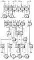
【0004】
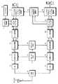
図1は、この発明を適用することが可能なソフトウェア無線装置の一例を示す。アンテナ(1a)から受信された中心周波数fcの信号はアンテナスイッチ(1b)を通り、ローノイズアンプ(1j)に入力される。ローノイズアンプから出力された信号は、受信ミキサ(1k)において、第1局部発振器(1c)の発振周波数f11をミックスされ、中間周波数fi の信号に変換される。
【0005】
中間周波数fi に変換された信号は、直交検波器(1l)において、第2局部発振器(1d)の中間周波数f12により直交検波され、アナログベースバンド信号I、Qに変換される。アナログベースバンド信号I、Qは、A/D変換器(1m)において、ディジタルベースバンド信号I−D、Q−Dに変換される。ディジタルベースバンド信号I−D、Q−Dがデマルチプレクサ(1p)に供給される。
【0006】
デマルチプレクサ(1p)によって、ソフトウェアの伝送パケットまたは情報データの伝送パケットの選択が行われる。ソフトウェアダウンロード時は、A/D変換器の出力データI−DとQ−Dがソフトウェア変調信号復調部(1o)で復調される。復調されたプログラムがプログラム可能なベースバンドディジタル変調部(1i)またはプログラム可能なベースバンドディジタル復調部(1n)にダウンロードされる。ダウンロード後にデマルチプレクサ(1p)は、A/D変換器の出力データI−DとQ−Dをプログラム可能なベースバンドディジタル復調部(1n)に供給し、プログラムによって決められた所望の復調処理が行われる。
【0007】
プログラム可能なベースバンドディジタル変調部(1i)およびプログラム可能なベースバンドディジタル復調部(1n)は、一例として、ソフトウェア変調信号復調部(1o)からのプログラムによって、OFDM(orthogonal frequency divisionmultiplexing:直交周波数分割多重)方式の変調および復調の機能と、W−CDMA(Wideband-CDMA:広帯域符号分割多元接続)方式の変調および復調の機能とが切り替えられるものである。この変復調方式は、マルチモード無線機の一例であって、この発明は、GSM(Global System for Mobile Communication:欧州のディジタル自動車・携帯電話の方式)等をプログラムによって実現しても良い。さらに、移動通信に限らず、この発明は、無線LANにおける異なる方式、ITS(Intelligent Transport System:高度道路交通システム)における異なる方式等に対しても適用可能である。
【0008】
相手先の局にダウンロードすべきソフトウェアを送信するときはソフトウェアメモリ(1q)に格納されたソフトウェアがソフトウェア変調部(1r)によって変調され、マルチプレクサ(1s)を通ったディジタルIQ信号I−D,Q−DがD/A変換器(1h)に入力される。D/A変換器(1h)は、ディジタルIQ信号をアナログ信号に変換する。情報ビットを送信するときは、変調データビットをプログラム可能なベ一スバンドディジタル変調部(1i)によって所望の変調方式で変調する。変調部(1i)の出力がマルチプレクサ(1s)を通り、ディジタルベースバンド信号I−D,Q−DとしてD/A変換器(1h)に入力される。なお、ソフトウェアメモリ(1q)およびソフトウェア変調部(1r)は、基地局に限らず、端末局が有することも可能である。
【0009】
アナログ信号は、直交変調器(1g)において、第2局部発振器(1d)の発振周波数f12により直交変調され、中間周波数fi(=f12)の信号に変換される。中間周波数fiに変調された信号は、送信ミキサ(1f)において、第1局部発振器(1c)の周波数f11により、周波数fc (=f12+f11)の信号に変換される。
【0010】
周波数fcに変換されたOFDM変調信号は、パワーアンプ(1e)において、所定の送信電力に増幅される。増幅された信号は、アンテナスイッチ(1b)を介して、アンテナ(1a)に供給され、送信される。MMAC(Mu1timedia mobi1e accesscommunication system)やWCDMA(Wideband code division mu1tip1e access)のような広帯域のスペクトラムを使用する移動体無線通信においては、A/D変換器(1m)とD/A変換器(1h)のサンプリング周波数が数十MSPS(Mega samples per second)となる。
【0011】
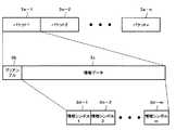
図2は、ソフトウェア無線通信システム用のソフトウェアを無線ダウンロードするリンクのパケットの構成例、並びに情報データを伝送するリンクのパケットの構成例を示す。このリンクは、基地局から端末局へのダウンリンクである。パケットは、ソフトウェアを伝送するパケット(2a-1,2a-2,...,2a-k)と情報データを伝送する情報パケット(2b-1,2b-2,...,2b-n)から構成される。
【0012】
ソフトウェアパケットは、プリアンブル(2c)およびソフトウェア(2d)から構成される。ソフトウェア(2d)は、エラー検出のために付加されたCRC(Cyc1ic redundancy check)のためのデータ(2e)とマイクロプロセッサ(あるいはDSP)に入力するプログラムまたはFPGAを再構成するためのコンフィギュレーションデータ(2f)から構成される。情報パケットは、プリアンブル(2g)と情報シンボル(2h-1,2h-2,...,2h-m)から構成される。
【0013】
受信したデータに対して、既知信号であるプリアンブルが検出され、検出に基づいてパケットタイミング同期、周波数同期、伝送路等化がなされる。受信したソフトウェアに対してはCRCで誤り検出を行う。誤りが検出された場合はそのパケットは破棄して再送を要求する。誤りが検出されない場合のみ、プログラムを復調して、ACK信号(アクノリッジ信号)を送信して次のパケットの送信を促す。全プログラムが復調されたら、復調されたプログラムをベースバンドディジタル信号変調部(1i)および復調部(1n)にダウンロードし、所望の変復調方式に設定する。情報パケットを受信し、プリアンブル(2g)に対してパケットタイミング同期、周波数同期、伝送路等化を行った後に、情報パケット情報シンボル(2h-1,2h-2,...,2h-m)に対して設定された復調方式で情報データの復調が行われる。
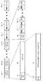
【0014】
図3は、ソフトウェア無線通信システムにおいて、ソフトウェアがダウンロードされた変調部によって、端末局から基地局に対して伝送するリンク(アップリンク)のパケットの構成例を示す。パケット(3a-1,3a-2,...,3a-n)は、既知信号であるプリアンブル(3b)と情報データ(3c)から構成される。情報データ(3c)は、情報シンボル(3d-1,3d-2,....,3d-m)から構成される。受信側では、プリアンブルの検出に基づいて、パケットタイミング同期、周波数同期、伝送路等化がなされ、その後に情報シンボルの復調が行われる。
【0015】
図4は、ソフトウェア無線通信システムのパケット再送処理例を示す。ソフトウェア無線通信システムにおいては、ソフトウェアがダウンロードされた変復調部によって本来伝送すべき情報データの変復調が行われる。無線伝送路によって発生したソフトウェアのエラーに起因して変復調部に故障が生じる可能性がある。したがって、ソフトウェアの無線伝送パケットに対してはCRCによるエラー検出が行われ、エラーフリー(エラー無し)となるまで何度も再送処理が行われる。
【0016】
例えばソフトウェア送信局からは最初のソフトウェアパケット1(4a)を送信する。受信したパケットに対してCRCによるエラー検出が行われ、エラーが検出されたら、送信局に対してエラーが検出されなくなるまで再送要求信号(4b)を送信する。図4は、2回の再送要求を行った後に送信されたソフトウェアパケット1(4e)でエラーフリーとなる例であるので、同一のパケット(4a,4c,4e)を3回再送している。エラーフリーとなった後では、ACK信号(4f)をソフトウェアの送信側に対して送信する。
【0017】
これらの動作を繰り返した後に最終のソフトウェアパケットk(4k)を受信し、全てのソフトウェアの復調が完了する。復号したソフトウェアがプログラム可能な変復調部にダウンロードされ、所望の変復調処理が可能となる。最終のソフトウェアパケットk(4k)に対するACK信号(41)を送信したのちに、情報パケット(4m,4n,....,4o)が伝送される。
【0018】
次に、図1のプログラム可能なベースバンドディジタル復調部(1n)の処理内容について説明する。一般的に変調部よりも復調部の処理が複雑であるので、復調部のみを説明する。一例として、広帯域のスペクトラムを使用する移動体無線通信システムであるMMACとWCDMAの復調部の構成について説明する。
【0019】
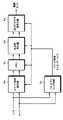
図5は、MMAC用のOFDM復調部の構成例を示す。入力されたディジタルベースバンド信号I−DとQ−Dは、まず、パケットタイミング同期部(5a)でパケットのタイミング同期を得た後に、キャリア周波数同期部(5b)でキャリア周波数を同期させ、メモリ(5c)にてデータを書き込んだ後に、FFT(fast Fourier transform)(5d)によって周波数領域に変換を行う。サブキャリア数をNFFTとすれば、FFT(5d)において、NFFT点の高速フーリエ変換をされ、すなわちNFFT点のパラレル受信データに復調される。その後に等化器(5e)によって伝送路等化が行われて誤り訂正符号復号化器(5f)によって誤りビットの訂正を行い復調ビットとして出力する。
【0020】
図6は、WCDMA用のスペクトラム拡散方式復調部の構成例を示す。入力されたディジタルベースバンド信号I−DとQ−Dは、まず、パケットタイミング同期部(6a)でパケットのタイミング同期を得た後に、キャリア周波数同期部(6b)でキャリア周波数を同期させる。メモリ(6c)にてデータを書き込んだ後に、逆拡散・等化部(6d)によって所定の拡散符号を用いて逆拡散と伝送路等化が行われる。逆拡散・等化部(6d)の出力が誤り訂正符号復号化器(6e)に供給され、復号化器(6e)によって誤りビットの訂正がなされ、復調ビットが出力される。
【0021】
上述の図5および図6に示したような復調部においては、数十MSPSのレートで入力されるサンプリングデータに対して実時問でFFT、逆拡散、等化器等の処理を行う必要がある。ソフトウェア無線通信システムにおいては、これらの処理をプログラム可能なハードウェアで実現する。プログラマブルデバイスとして数百MHzのクロックで動作する超高速な汎用マイクロプロセッサの使用も考えられる。しかしながら、消費電力がクロック周波数に依存するために、電池で動作するような実用的な携帯情報端末装置の設計は困難である。
【0022】
プログラマブルデバイスとして、FPGAを用いることによって、比較的低消費電力で、かつ高速な復調用の信号処理ハードウェアが実現できる。100万ゲートを超える大規模なFPGAも市場に出始めているため、140万ゲートを超えるMMAC用のOFDM LSIの機能も数個のFPGAを用いれば十分に実現可能である。但し、FPGAを所望の機能にプログラムするためにはFPGA内部の再構成可能な論理回路の機能、および論理回路間の結線等をプログラムするためのコンフィギュレーションデータが必要となる。前述したMMAC用のOFDM LSIをプログラムするためには8Mビットものコンフィギュレーションデータが必要となる。
【0023】
この明細書の説明では、「ソフトウェア」または「プログラム」という用語にはFPGAの機能を定義するコンフィギュレーションデータも含まれる。
【0024】
べースバンド処理部を構成するFPGAについて説明する。図7にFPGAの内部構成を示す。まず、FPGAチップ(7a)には、外部からコンフィギュレーションデータが供給され、コンフィギュレーションメモリ(7c)に書き込まれる。このデータによって各部の回路の機能がプログラムされる。
【0025】
プログラム可能な論理回路ブロックであるCLB(Configurab1e 1ogic b1ock)(7g)は、対応するコンフィギュレーションデータによって、ユーザが所望する小規模な論理回路に構成できる。IOB(Input/output b1ocks)(7d)はチップ外とチップ内の信号のインタフェース回路であり、一種の電流増幅器でもある。対応するコンフィギュレーションデータによって所定の論理振幅電圧に設定され、外部論理電圧を内部の論理電圧に変換する機能を有する。RC(Routing channe1)(7e)は各ブロックを接続するデータバスであり、CLB間とIOB間またはCLBとIOB間のデータ転送が行われる。プログラム可能なスイッチであるPSM(Programmab1e switch matrix)(7f)とCB(Connection Block)(7h)は、マトリクス状に配置され、RC間の接続を対応コンフィギュレーションデータに応じて設定し、各ブロック間でのデータの授受を可能とする。
【0026】
図8は、CLBの内部構成例を示す。CLBは、4入力1出力のLUT(Look-up tab1e)(8a,8b)および、3入力1出力のLUT(8c)、キャリ生成用専用のプログラム可能な論理回路であるCL(Carry 1ogic)(8d,8e)、9個のマルチプレクサ(8f,8g,8h,8i,8j,8k,81,8m,8n)と2個のレジスタ(8o,8p)から構成される。CLBはSRAMであり、入力はアドレスに相当する。4入力と3入力のCLBに対して、それぞれ16ビットと8ビットのコンフィギュレーションデータをダウンロードして任意の論理回路を構成することができる。[表1]に4入力のLUTの真理値表の例を示す。
【0027】
【表1】
CLは、対応するコンフィギュレーションデータによって、あらかじめ定義されているいくつかの論理回路の一つを実現できる。また、各マルチプレクサの制御用信号もコンフィギュレーションデータによって設定される。種々のコンフィギュレーションデータをCLBに与えることによって、レジスタを含む所望の論理回路を実現することができる。
【0029】
以上のように、図7で示したコンフィギュレーションメモリからIOB,PSM,CB,CLBにコンフィギュレーションデータを供給することによって所望の仕様の論理回路をFPGAによって実現できる。
【0030】
FPGAのブロックを使用して設計した加算器、乗算器、および、任意の2入力演算回路を以下に説明する。説明を簡単にするために、以下では、特に言及しない場合は、LUTの内容とCL設定データをコンフィギュレーションデータと呼ぶことにする。
【0031】
図9は、FPGAのLUTとCLで設計した9ビット加算器の構成例を示す。桁上げ信号が下位ビットから伝播するリップルキャリ型加算器である。2の補数で表現された入力データバスのビットa8-a0とb8−b0はまず初段のLUT(9a-1,9a-2,9a-3,9a-4,9a-5,9a-6,9a-7,9a-8,9a-9,9a-10)に入力される。LUT(9a-1)はオーバフローが発生したことを表す制御信号を生成する。それ以外のLUTは、重みの等しい2つのビットのデータと下位ビットからの桁上げ信号との和を計算する。
【0032】
CL(9b-1,9b-2,9b-3,9b-4,9b-5,9b-6)は、入力データバスの対応する各ビットにおける桁上げ信号の生成と下位ビットから上位ビットヘの桁上げ信号の伝播を行う。最終段のLUT(9c-1,9c-2,9c-3,9c-4,9c-5,9c-6,9c-7,9c-8)では和出力に対する2の補数表現に対応した符号処理とオーバフロー時の飽和処理が行われる。この例以外にも種々の加算器のアルゴリズムが提案されている。
【0033】
図10は、FPGAのLUTとCLを使用して設計した3×2ビットの乗算器の構成例を示す。2の補数で表現された入力データa2,a1,a0とb1,b0は、それぞれ対応するLUT(10a-1,10a-2,10a-3)、LUT(10a-5,10a-6)およびCL(10b-1,10b-2,10b-3)によって絶対値に変換される。LUT(1Oa-4)によって積の符号が決定する。絶対値の各ビットa'2,a'1,a0'とb'1,b'0がLUT(10c-1,10c-2,...,10c-6)に供給され、LUT(10c-1,10c-2,...,10c-6)によって部分積の計算が行われる。部分積はLUT(10d-1,10d-2,10d-3)、CL(1Oe-1,10e-2)、LUT(10f-1,10f-2,...,10f-5)およびCL(10g-1,10g-2,10g-3,10g-4)から構成された加算木で加算されて積が算出される。
【0034】
任意の2入力演算回路をLUTによって設計する。表2は、データの語長が12ビットの2入力1出力演算回路の真理値表の例を[表2]として示す。
【0035】
【表2】
図11は、この真理値表に基づいてLUTによって設計した演算回路の構成例を示す。入力データのビット数の合計が24ビットであるため、24入力1出力の論理回路を12個用意すれば実現可能である。出力ビットc11(MSB),c10,...,c0(LSB)は、論理回路(1111,1110,...,110)によって算出される。各論理回路は、24ビットのデータを入力する8個のLUT(11a-1,11a-2,11a-3,11a-4,11a-5,11a-6,11a-7,11a-8)から構成される。
【0037】
真理値表(表2)を満足するようにコンフィギュレーションデータが各論理回路の各LUTに書き込まれる。図11に示した構成は、LUTを直接的に木状に接続して設計したため、LUTの個数が最大の例である。真理値表の内容によっては、論理式の簡単化を行うことによってLUTの数を削減することが可能である。
【0038】
図5と図6中に示したタイミング同期部(5a,6a), キャリア周波数同期部(5b,6b)、FFT(5d)、逆拡散・等化部(6d)においては、主に相関演算がなされ、OFDMの伝送路等化(5e)の処理では除算が行われる。すなわち、FPGA上で処理回路を構成するためには、乗算器、加算器、および除算器が必要となる。入力データは数十MHzのサンプリングレートで入力され、実時間で演算を行う必要がある。FPGAのLUTやCLで構成した演算回路の演算時間が数十nsecであると仮定すれば、ハードウェアを時分割的に共有することは困難であり、各処理部毎にそれぞれの演算回路が必要となる。したがって、ベースバンドの変復調処理全体を構成するためには、膨大な数のLUTやCLが必要である。例えば、MMAC用のFFTのみをFPGA上で実現するには2300個以上のLUTと同数程度のCLが必要である。これらをプログラムするための大量のコンフィギュレーションデータが必要となる。さらに、MMAC用のOFDMの変復調LSIは140万ゲート以上の規模であるから、これをFPGAで構成すると仮定すれば、8Mビット以上のコンフィギュレーションデータが必要となる。
【0039】
【発明が解決しようとする課題】
図4に示したように、従来のソフトウェアの無線ダウンロード手法においては、受信したソフトウェアに対してCRCを行い、エラーフリーが確認された後にプログラマブルデバイスにダウンロードが行われる。誤りが検出された場合はエラーフリーになるまで再送要求が行われる。この手法は、劣悪な伝搬環境下においては、エラーフリーに到達するまで膨大な量のコンフィギュレーションデータを何度も再送する必要があり、ダウンロードが完了するまでに膨大な時問が費やされる。
【0040】
コンフィギュレーションデータのダウンロード時間が増大すれば、図2のパケット構成図に示されるような本来伝送すべき情報データの伝送効率は劣化する。また、時々刻々と変動する伝搬路環境に応じて最適な機能を無線ダウンロードして実現する適応伝送方式においては、機能を実現するためのコンフィギュレーションデータの伝送は速やかに行われる必要がある。再送をともなう伝送方式では、無線ダウンロードが完了するまでに伝搬環境が激変してしまい、ダウンロード完了後の伝搬環境に最適な機能をFPGA上で実現できない。したがって、ソフトウェア無線通信システムの特長を活用するにはFPGAのコンフィギュレーションデータを含めたソフトウェアの高効率な無線伝送・ダウンロード手法の確立が必須である。
【0041】
したがって、この発明の目的は、FPGAのコンフィギュレーションデータのようなプログラムの伝送効率を向上させることができる無線通信装置、プログラム送信装置およびその方法、並びに無線通信システムを提供することにある。
【0042】
【課題を解決するための手段】
上述した課題を解決するために、請求項1の発明は、ハードウェアの一部または全部がプログラム可能な論理回路で構成され、論理回路に対するプログラムを受信することによって、所望の無線通信方式を実現するようにした無線通信装置において、
プログラム可能な論理回路で構成された2進数演算回路の論理回路がその入出力の各ビットに対応する2のべき乗の重みの大きさによって少なくとも第1および第2の二つのグループに分割され、
重みの大きい第1のグループの論理回路に対する第1のプログラムがビット誤りが少ない第1の方式で変調されて伝送され、重みの小さい第2のグループの論理回路に対するプログラムが伝送効率が優れた第2の方式で変調されて伝送されるようにした無線通信装置である。
【0043】
請求項3の発明は、ハードウェアの一部または全部がプログラム可能な論理回路で構成され、論理回路に対するプログラムを受信することによって、所望の無線通信方式を実現するようにした無線通信装置において、
プログラム可能な論理回路で構成された2進数演算回路の論理回路がその入出力の各ビットに対応する2のべき乗の重みの大きさによって少なくとも第1および第2の二つのグループに分割され、
重みの大きい第1のグループの論理回路に対する第1のプログラムは、誤り訂正能力の高い符号化方式を用いて伝送され、重みの小さい第2のグループの論理回路に対する第2のプログラムは、符号化率の高い符号化方式を用いて伝送されるようにした無線通信装置である。
【0044】
請求項4の発明は、ハードウェアの一部または全部がプログラム可能な論理回路で構成され、論理回路に対するプログラムを受信することによって、所望の無線通信方式を実現するようにした無線通信装置において、
プログラム可能な論理回路で構成された2進数演算回路の論理回路がその入出力の各ビットに対応する2のべき乗の重みの大きさによって少なくとも第1および第2の二つのグループに分割され、
重みの大きい第1のグループの論理回路に対する第1のプログラムが低速なシンボルレートで変調されて伝送され、重みの小さい第2のグループの論理回路に対するプログラムが高速なシンボルレートで変調して伝送されるようにした無線通信装置である。
【0045】
請求項5の発明は、ハードウェアの一部または全部がプログラム可能な論理回路で構成され、論理回路に対するプログラムを受信することによって、所望の無線通信方式を実現するようにした無線通信装置において、
プログラム可能な論理回路が演算回路と非演算回路に分割され、演算回路に対する一部の第1のプログラムは、再送処理を施さずに伝送され、演算回路の一部および非演算回路に対する第2のプログラムは再送処理を施して信頼性を高めて伝送されるようにした無線通信装置である。
【0046】
請求項7の発明は、ハードウェアの一部または全部がプログラム可能な論理回路で構成され、論理回路に対するプログラムを受信することによって、所望の無線通信方式を実現するようにした無線通信装置において、
プログラム可能な論理回路で構成された2進数演算回路の論理回路がその入出力の各ビットに対応する2のべき乗の重みの大きさによって少なくとも第1および第2の二つのグループに分割され、
重みの大きい第1のグループの論理回路に対する第1のプログラムは、第1の変調方式、第1の誤り訂正符号および第1のシンボルレートの内の2以上を組み合わせた伝送方式で伝送され、
重みの小さい第2のグループの論理回路に対する第2のプログラムは、第2の変調方式、第2の誤り訂正符号および第2のシンボルレートの内の2以上を組み合わせた伝送方式で伝送され、
第1の変調方式は、第2の変調方式に比して誤りが少ないものとされ、
第1の誤り訂正符号は、第2の誤り訂正符号に比して誤り訂正能力の高いものとされ、
第1のシンボルレートは、第2のシンボルレートに比して低いものとされた無線通信装置である。
【0047】
請求項8の発明は、ハードウェアの一部または全部がプログラム可能な論理回路で構成され、論理回路に対するプログラムを受信することによって、所望の無線通信方式を実現するようにした無線通信装置において、
プログラム可能な論理回路で構成された2進数演算回路の論理回路がその入出力の各ビットに対応する2のべき乗の重みの大きさによって少なくとも第1および第2の二つのグループに分割され、
第1および第2のプログラムが比較的値数の多い変調方式を使用して伝送され、
重みの大きい第1のグループのプログラムは、変調方式の平均誤り率よりも優れた伝送が可能なビット位置に割り当てられ、重みが小さい第2のグループのプログラムは、変調方式の平均誤り率よりも劣った伝送特性を有するビット位置に割り当てられる無線通信装置である。
【0048】
請求項12の発明は、ハードウェアの一部または全部がプログラム可能な論理回路で構成され、論理回路に対するプログラムを受信することによって、所望の無線通信方式を実現するようにした無線通信装置に対してプログラムを送信する送信方法において、
プログラム可能な論理回路で構成された2進数演算回路の論理回路がその入出力の各ビットに対応する2のべき乗の重みの大きさによって少なくとも第1および第2の二つのグループに分割され、
重みの大きい第1のグループの論理回路に対する第1のプログラムをビット誤りが少ない第1の方式で変調し伝送し、重みの小さい第2のグループの論理回路に対するプログラムを伝送効率が優れた第2の方式で変調して伝送するようにしたプログラム送信装置である。請求項22の発明は、このようにプログラムを送信する方法である。
【0049】
請求項14の発明は、ハードウェアの一部または全部がプログラム可能な論理回路で構成され、論理回路に対するプログラムを受信することによって、所望の無線通信方式を実現するようにした無線通信装置に対してプログラムを送信する送信装置において、
プログラム可能な論理回路で構成された2進数演算回路の論理回路がその入出力の各ビットに対応する2のべき乗の重みの大きさによって少なくとも第1および第2の二つのグループに分割され、
重みの大きい第1のグループの論理回路に対する第1のプログラムを誤り訂正能力の高い符号化方式を用いて伝送し、重みの小さい第2のグループの論理回路に対する第2のプログラムを符号化率の高い符号化方式を用いて伝送するようにしたプログラム送信装置である。請求項24の発明は、このようにプログラムを送信する方法である。
【0050】
請求項15の発明は、ハードウェアの一部または全部がプログラム可能な論理回路で構成され、論理回路に対するプログラムを受信することによって、所望の無線通信方式を実現するようにした無線通信装置に対してプログラムを送信する送信装置において、
プログラム可能な論理回路で構成された2進数演算回路の論理回路がその入出力の各ビットに対応する2のべき乗の重みの大きさによって少なくとも第1および第2の二つのグループに分割され、
重みの大きい第1のグループの論理回路に対する第1のプログラムを低速なシンボルレートで変調して伝送し、重みの小さい第2のグループの論理回路に対するプログラムを高速なシンボルレートで変調して伝送するようにしたプログラム送信装置である。請求項24の発明は、このようにプログラムを送信する方法である。
【0051】
請求項16の発明は、ハードウェアの一部または全部がプログラム可能な論理回路で構成され、論理回路に対するプログラムを受信することによって、所望の無線通信方式を実現するようにした無線通信装置に対してプログラムを送信する送信装置において、
プログラム可能な論理回路が演算回路と非演算回路に分割され、演算回路に対する一部の第1のプログラムを再送処理を施さずに伝送し、演算回路の一部および非演算回路に対する第2のプログラムを再送処理を施して信頼性を高めて伝送するようにしたプログラム送信装置である。請求項26の発明は、このようにプログラムを送信する方法である。
【0052】
請求項18の発明は、ハードウェアの一部または全部がプログラム可能な論理回路で構成され、論理回路に対するプログラムを受信することによって、所望の無線通信方式を実現するようにした無線通信装置に対してプログラムを送信する送信装置において、
プログラム可能な論理回路で構成された2進数演算回路の論理回路がその入出力の各ビットに対応する2のべき乗の重みの大きさによって少なくとも第1および第2の二つのグループに分割され、
重みの大きい第1のグループの論理回路に対する第1のプログラムを第1の変調方式、第1の誤り訂正符号および第1のシンボルレートの内の2以上を組み合わせた伝送方式で伝送し、
重みの小さい第2のグループの論理回路に対する第2のプログラムを第2の変調方式、第2の誤り訂正符号および第2のシンボルレートの内の2以上を組み合わせた伝送方式で伝送し、
第1の変調方式は、第2の変調方式に比して誤りが少ないものとされ、
第1の誤り訂正符号は、第2の誤り訂正符号に比して誤り訂正能力の高いものとされ、
第1のシンボルレートは、第2のシンボルレートに比して低いものとされたプログラム送信装置である。請求項28の発明は、このようにプログラムを送信する方法である。
【0053】
請求項19の発明は、ハードウェアの一部または全部がプログラム可能な論理回路で構成され、論理回路に対するプログラムを受信することによって、所望の無線通信方式を実現するようにした無線通信装置に対してプログラムを送信する送信装置において、
プログラム可能な論理回路で構成された2進数演算回路の論理回路がその入出力の各ビットに対応する2のべき乗の重みの大きさによって少なくとも第1および第2の二つのグループに分割され、
第1および第2のプログラムを比較的値数の多い変調方式を使用して伝送し、重みの大きい第1のグループのプログラムを変調方式の平均誤り率よりも優れた伝送が可能なビット位置に割り当て、重みが小さい第2のグループのプログラムを変調方式の平均誤り率よりも劣った伝送特性を有するビット位置に割り当てるプログラム送信装置である。請求項29の発明は、このようにプログラムを送信する方法である。
【0054】
請求項32の発明は、ハードウェアの一部または全部がプログラム可能な論理回路で構成され、論理回路に対するプログラムを受信することによって、所望の無線通信方式を実現するようにした無線通信装置と、無線通信装置に対してプログラムを送信する送信装置とからなる無線通信システムにおいて、
無線通信装置は、プログラム可能な論理回路で構成された2進数演算回路の論理回路がその入出力の各ビットに対応する2のべき乗の重みの大きさによって少なくとも第1および第2の二つのグループに分割され、
送信装置は、重みの大きい第1のグループの論理回路に対する第1のプログラムをビット誤りが少ない第1の方式で変調し伝送し、重みの小さい第2のグループの論理回路に対するプログラムを伝送効率が優れた第2の方式で変調して伝送するようにした無線通信システムである。
【0055】
請求項33の発明は、ハードウェアの一部または全部がプログラム可能な論理回路で構成され、論理回路に対するプログラムを受信することによって、所望の無線通信方式を実現するようにした無線通信装置と、無線通信装置に対してプログラムを送信する送信装置とからなる無線通信システムにおいて、
無線通信装置は、プログラム可能な論理回路で構成された2進数演算回路の論理回路がその入出力の各ビットに対応する2のべき乗の重みの大きさによって少なくとも第1および第2の二つのグループに分割され、
送信装置は、重みの大きい第1のグループの論理回路に対する第1のプログラムを誤り訂正能力の高い符号化方式を用いて伝送し、重みの小さい第2のグループの論理回路に対する第2のプログラムを符号化率の高い符号化方式を用いて伝送するようにした無線通信システムである。
【0056】
請求項34の発明は、ハードウェアの一部または全部がプログラム可能な論理回路で構成され、論理回路に対するプログラムを受信することによって、所望の無線通信方式を実現するようにした無線通信装置と、無線通信装置に対してプログラムを送信する送信装置とからなる無線通信システムにおいて、
無線通信装置は、プログラム可能な論理回路で構成された2進数演算回路の論理回路がその入出力の各ビットに対応する2のべき乗の重みの大きさによって少なくとも第1および第2の二つのグループに分割され、
送信装置は、重みの大きい第1のグループの論理回路に対する第1のプログラムを低速なシンボルレートで変調して伝送し、重みの小さい第2のグループの論理回路に対するプログラムを高速なシンボルレートで変調して伝送するようにした無線通信システムである。
【0057】
請求項35の発明は、ハードウェアの一部または全部がプログラム可能な論理回路で構成され、論理回路に対するプログラムを受信することによって、所望の無線通信方式を実現するようにした無線通信装置と、無線通信装置に対してプログラムを送信する送信装置とからなる無線通信システムにおいて、
無線通信装置は、プログラム可能な論理回路が演算回路と非演算回路に分割され、
送信装置は、演算回路に対する一部の第1のプログラムを再送処理を施さずに伝送し、演算回路の一部および非演算回路に対する第2のプログラムを再送処理を施して信頼性を高めて伝送するようにした無線通信システムである。
【0058】
請求項36の発明は、ハードウェアの一部または全部がプログラム可能な論理回路で構成され、論理回路に対するプログラムを受信することによって、所望の無線通信方式を実現するようにした無線通信装置と、無線通信装置に対してプログラムを送信する送信装置とからなる無線通信システムにおいて、
無線通信装置は、プログラム可能な論理回路で構成された2進数演算回路の論理回路がその入出力の各ビットに対応する2のべき乗の重みの大きさによって少なくとも第1および第2の二つのグループに分割され、
送信装置は、重みの大きい第1のグループの論理回路に対する第1のプログラムを第1の変調方式、第1の誤り訂正符号および第1のシンボルレートの内の2以上を組み合わせた伝送方式で伝送し、
重みの小さい第2のグループの論理回路に対する第2のプログラムを第2の変調方式、第2の誤り訂正符号および第2のシンボルレートの内の2以上を組み合わせた伝送方式で伝送し、
第1の変調方式は、第2の変調方式に比して誤りが少ないものとされ、
第1の誤り訂正符号は、第2の誤り訂正符号に比して誤り訂正能力の高いものとされ、
第1のシンボルレートは、第2のシンボルレートに比して低いものとされた無線通信システムである。
【0059】
請求項37の発明は、ハードウェアの一部または全部がプログラム可能な論理回路で構成され、論理回路に対するプログラムを受信することによって、所望の無線通信方式を実現するようにした無線通信装置と、無線通信装置に対してプログラムを送信する送信装置とからなる無線通信システムにおいて、
無線通信装置は、プログラム可能な論理回路で構成された2進数演算回路の論理回路がその入出力の各ビットに対応する2のべき乗の重みの大きさによって少なくとも第1および第2の二つのグループに分割され、
送信装置は、第1および第2のプログラムを比較的値数の多い変調方式を使用して伝送し、
重みの大きい第1のグループのプログラムを変調方式の平均誤り率よりも優れた伝送が可能なビット位置に割り当て、重みが小さい第2のグループのプログラムを変調方式の平均誤り率よりも劣った伝送特性を有するビット位置に割り当てる無線通信システムである。
【0060】
この発明では、プログラム可能な論理回路に対するプログラムを重要度に応じて伝送方式を異ならせる。すなわち、プログラムのエラーの影響が大きいものとそうでないものとに分け、エラーの影響が大きいものについては、伝送時にエラーが発生しにくいように伝送し、エラーの影響が相対的に小さいものについては、伝送効率を重視して伝送する。
【0061】
【発明の実施の形態】
以下、この発明の実施形態について説明する。この発明の理解の容易のために、最初にプログラム可能な論理回路例えば演算回路について説明する。一般的に、FFT、相関器、ディジタルフィルタ等のディジタル無線通信用の主要な信号処理回路は2進数演算に基づく加算器、減算器、乗算器で構成されている。FPGAではこれらの演算回路は多数のLUTを使用して構成される。2進数系に基づく演算器ならば、データバスの各ビットには2のべき乗の重みが付けられている。データバスの各ビットはLUTの入出力に接続されている。
【0062】
無線伝送されたコンフィギュレーションデータには、誤りビットが発生する。その誤りビットによって演算結果に誤差が発生する。LUTの扱うビットに付けられている重みによって演算結果に及ぼす影響が異なる。誤りビットの個数と位置が同じ16ビットのコンフィギュレーションデータを有する4入力1出力のLUTが演算器の入出力バスのLSBに接続されていた場合、データのダイナミックレンジに対して演算誤差が小さいために、演算誤差の影響は小さい。
【0063】
しかしながら、LUTが演算器の入出力バスのMSBに接続されていた場合、データのダイナミックレンジに対して演算誤差が比較的大きくなるために、演算誤差が結果に対して著しい影響を与える。すなわち、LUTのコンフィギュレーションデータの誤りがコンフィギュレーションデータでプログラムされた通信装置の伝送品質、例えば、BER(Bit error rate)に与える影響は、コンフィギュレーションデータの誤りを含むLUTが2進数のどの桁に対する処理を行っているかによって異なる。
【0064】
例えば、図9に示した9ビット加算器であれば、入出力のデータバスの各ビットにはLSBからMSBについてそれぞれ20,21,22,23,24,25,26,27,−28の重みが付けられている。和出力データバスのLSBに接続されたLUT(9c-8)とMSBに接続されたLUT(9a-2)に着目すれば、両LUTのコンフィギュレーションデータに同様の誤りビットが発生していた場合、和の出力データバスに発生する誤差の最大値はそれぞれ20と−28となり、MSBに接続されたLUT(9a-2)のコンフィギュレーションデータの誤りビットの及ぼす影響が大きい。復調器の回路の一部であれば、BERに及ぼす影響も同様に大きい。
【0065】
このような点を考慮して、この発明においては、演算器のオペランドのデータバスを複数のグループに分割する。説明を簡単にするために、データバスのビットに接続されているLUTを2つのスライスに分割する。MSB側のLUT群とCL群をMSBスライスと呼び、LSB側のLUT群とCL群をLSBスライスと呼ぶことにする。広義の意味としてスライスは、LUTとCLのコンフィギュレーションデータをも含むものとする。例えば、両スライスの入出力データビットの重みを比較すればMSBスライスに属するLUTの扱うビットの重みのほうが大きい。すべてのLUTのコンフィギュレーションデータに同じ確率で誤りが発生したと仮定すると、MSBスライスに属するLUTのほうが、LSBスライスに属するLUTよりも演算結果の誤差が大きく、復調器のBERを劣化させる影響は大きい。
【0066】
したがって、MSBスライスに対してはビット誤りが発生し難い伝送特性の優れた伝送方式を適用し、一方、LSBスライスに対しては伝送特性が劣っても伝送効率の優れた伝送方式を適用する。このように、両スライスに対して伝送方式を使い分けることによって全体のシンボル数を減少できるため伝送時間を削減できる。以下、この発明を上述したいくつかの演算回路に適用した場合のスライス分割について説明する。
【0067】
図12は、9ビット加算器において、オペランド入力と和出力のデータパスに対して、LUTをMSBスライスとLSBスライスに分割した例を示す。CLのコンフィギュレーションデータを16ビットと仮定する。オペランド側と和側でのMSBスライスに属するLUTの数をそれぞれ、6個と3個とすれば、LSBスライスに属するLUTの数は、それぞれ4個と5個とである。CLについてはMSBスライスとLSBスライスに属する数はいずれも3個である。コンフィギュレーションデータのビット数は、それらの個数にLUTとCLのコンフィギュレーションデータのビット数である16を掛けた値となる。
【0068】
MSBスライスのコンフィギュレーションビットは12×16=192ビットとなり、LSBスライスのコンフィギュレーションビットは12×16=192ビットとなる。
【0069】
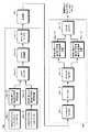
図13は、図10に示した3×2ビットの乗算器についてスライス分割を行った場合の構成例を示す。図13において、MSBスライスに割り当てられるLUTおよびCLは、ブロック内のこれらの文字に対して下線を付して示す。一方、LSBスライスに対して割り当てられるLUTおよびCLは、ブロック内のこれらの文字に対して下線を付さないで示す。絶対値への変換を行うLUTを入力バスのa2,a1,a0とb1,b0に対してMSBから、それぞれ2個と1個づつのLUT(13a-1,13a-2,13a-5)をMSBスライスに割り当てる。さらに積の符号を出力するLUT(13a-4)、部分積を演算するLUT(13c-1,13c-2,13c-3)、加算木のLUT(13d-1,13d-2)、CL(13e-1)、LUT(13f-1,13f-2,13f-3)、およびCL(13g-1,13g-2,13g-3)をMSBスライスに割り当てる。MSBスライスに属するLUTとCLのコンフィギュレーションデータが18×16=288ビットとなる。LSBスライスについては、コンフィギュレーションデータが11×16=176ビットとなる。
【0070】
図14および図15は、図11に示した任意の2入力演算回路に対してスライスを行った場合の構成例を示す。作図スペースの制約によって、本来は一つの図を図14および図15の二つに分割している。図14および図15において、MSBスライスに割り当てられるLUTおよびCLは、ブロック内のこれらの文字に対して下線を付して示す。一方、LSBスライスに対して割り当てられるLUTおよびCLは、ブロック内のこれらの文字に対して下線を付さないで示す。図14に示すように、MSBであるc11を出力する論理回路(1411)内の全てのLUT(14a-1,14a-2,...,14a-8)のコンフィギュレーションデータをMSBスライスに割り当てる。c10を出力する論理回路(1410)内のLUTにおいては、入力データバスのMSBビットに近いLUT(14b-1,14b-2,14b-4,14b-5,14b-7,14b-8)のコンフィギュレーションデータをMSBスライスに割り当てる。図15に示すように、LSBのc0を出力する論理回路(140)についてはMSBビットを扱うLUT(14c-1,14c-4)およびデータパスの中問に存在するLUT(14c-7,14c-8)のコンフィギュレーションデータをMSBスライスに割り当てる。
【0071】
前述した例は主として演算回路であるが、演算回路以外のクロック信号を扱う回路、機能を決定する制御信号を生成または受信する回路、CLB間の接続を決定するPMSとCBの制御信号、CLB内のマルチプレクサ制御信号および、ビット単位で論理演算を行いかつ高い信頼性が要求される誤り訂正符号の符号化または復号化回路等を構成するためのコンフィギュレーションデータに対しても、この発明を適用することができる。演算回路以外の回路を構成するためのコンフィギュレーションデータに対してこの発明を適用した実施形態については後述する。
【0072】
また、コンフイギュレーションテータの伝送時問が等しくともコンフィギュレーションデータの誤りを減少させれば、ダウンロードされたハードウェアの故障率を減らせ信頼性を向上できる。この手法もコンフィギュレーションデータの伝送効率を向上できる手法として後述する。
【0073】
以下に分割した各スライスのコンフィギュレーションデータに対してこの発明を適用した複数の実施形態について説明する。
【0074】
この発明の第1の実施形態は、各スライスに対して異なる変調方式を適用するものである。MSBスライスのLUT用のコンフィギュレーションデータに対しては、伝送特性は優れたビット誤りが発生し難い伝送方式例えば多値数の少ないQPSK(quadrature phase shift keying )方式で変調を施す。逆にLSBスライスのLUT用のコンフィギュレーションデータに対しては、伝送特性が劣っても伝送効率の優れた伝送方式例えば多値数は多いが、伝送特性の劣る16QAM(Quadrature Amplitude Modulation) 変調を施す。16QAMで変調したコンフィギュレーションデータの誤りビット数が増加するが、LSB側のコンフィギュレーションデータのビット誤りに起因する演算誤差は比較的小さいと考えられる。この方式でコンフィギュレーションデータの伝送を行えば、BERを著しく劣化させずに、コンフィギュレーションデータを変調した伝送シンボル数を減少できる。
【0075】
9ビット加算器においては、図12を参照して説明した各スライスに対する割り当て結果より、MSBスライスは1シンボルあたり2ビットを伝送するQPSK変調であるので96シンボル、LSBスライスは1シンボルあたり4ビットを伝送する16QAM変調であるので、48シンボルとなり合計144シンボルが必要となる。両スライスともQPSK変調を行った場合は192シンボルが必要となる。したがって、全てをQPSKで変調した場合よりも約25パーセント、シンボル数、すなわち、コンフィギュレーションデータの伝送時間を削減できる。
【0076】
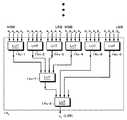
図16は、この発明の第1の実施形態によるコンフィギュレーションデータのべースバンドにおける伝送系を示す。伝送系は、コンフィギュレーションデータを無線伝送する送信機(15a)、伝送路(15b)、コンフィギュレーションデータを受信する受信機(15c)から構成される。受信機(15c)においてシンボルタイミング同期部、キャリア周波数同期部、伝送路等化部等の記述は省略している。
【0077】
MSBスライスに割り当てるLUTのコンフィギュレーションデータが格納されているメモリ(15a-1)からデータがQPSK変調器(15a-3)に供給される。LSBスライス側に割り当てるLUTのコンフィギュレーションデータが格納されているメモリ(15a-2)からデータが16QAM変調器(15a-4)に供給される。QPSK変調器(15a-3)および16QAM変調器(15a-4)の出力信号がマルチプレクサ(15a-5)によって時間軸上で結合させられ、ロールオフフィルタ(15a-6)によって帯域制限された後に伝送路(15b)へ送信される。
【0078】
受信側では、ロールオフフィルタ(15c-1)によって帯域を制限した後に、サンプラー(15c-2)によってシンボル周期でサンプリングを行う。サンプラー(15c-2)の出力がデマルチプレクサ(15c-3)に供給され、デマルチプレクサ(15c-3)によってQPSKの変調波形と16QAMの変調波形に分離され、それぞれがQPSK復調器(15c-4)と16QAM復調器(15c-5)によって復調される。各復調器で復調されたビットはマルチプレクサ(15c-6)において合成され、復調コンフィギュレーションデータとして出力される。
【0079】
次にこの発明の第2の実施形態について説明する。第2の実施形態は、異なる誤り訂正符号を使用するものである。MSBスライスに属するLUT用のコンフィギュレーションデータに対しては誤り訂正能力の高い誤り訂正符号への符号化を行う。この場合、一般的に符号化率は小さくなる。符号化率は、もともと情報を表しているビット数kと実際に伝送または蓄積されるビット数nとの比(k/n)を意味する。符号化率が高ければ、冗長度が小さい反面、誤り訂正能力が小さい。LSBスライスのコンフィギュレーションデータに対しては、符号化率が比較的高いが、誤り訂正能力がMSBスライスのコンフィギュレーションデータの符号化で使用した方式よりも劣る符号化方式を用いる。
【0080】
例えば9ビット加算器の例において、MSBスライスに対しては符号化率が1/2の符号化を行い、LSBスライスに対しては、3/4で行えば,符号化後のビット数は192×2+192×(4/3)=640ビットとなる。両スライスを1/2の符号化率で符号化を行った場合は384×2=768ビットであり、約17パーセントの伝送時間の削減が可能となる。
【0081】
第2の実施形態によるコンフィギュレーションデータのべースバンドにおける伝送系を図17に示す。伝送系は、コンフィギュレーションデータを無線伝送する送信機(16a)、伝送路(16b)、コンフィギュレーションデータを受信する受信機(16c)から構成される。受信機(16c)においてシンボルタイミング同期部、キャリア周波数同期部、伝送路等化部等の記述は省略している。変調方式は一例としてQPSKを仮定している。
【0082】
MSBスライスに属するLUTのコンフィギュレーションデータが格納されているメモリ(16a-1)からデータが符号化率=1/2の誤り訂正符号符号化器(16a-3)に供給される。LSBスライス側に属するLUTのコンフィギュレーションデータが格納されているメモリ(16a-2)からデータが符号化率3/4の誤り訂正符号符号化器(16a-4)に供給される。符号化器(16a-3)および(16a-4)によって符号化されたビットがマルチプレクサ(16a-5)によって結合される。その後に、QPSK変調器(16a-6)によって変調されロールオフフィルタ(16a-7)によって帯域が制限された後に伝送路(16b)へ送信される。
【0083】
受信側ではロールオフフィルタ(16c-1)によって帯域を制限した後にサンプラー(16c-2)によってシンボル周期でサンプリングを行う。サンプラー(16c-2)の出力がデマルチプレクサ(16c-3)に供給され、デマルチプレクサ(16c-3)によって、分離されたデータがそれぞれ符号化率の異なる誤り訂正符号復号化器(16c-4,16c-5)に供給される。図17の構成では、復号化器(16c-4,16c-5)が軟判定を行うと仮定している。なお、硬判定の復号を行う場合は、サンプラー(16c-2)とデマルチプレクサ(16c-3)の間にQPSK復調器が挿入され、ビットに復調した後に復号化器に分配されて復号が行われる。復号ビットは、マルチプレクサ(16c-6)によってビットの結合が行われてコンフィギュレーションデータとして出力される。異なる符号化率の符号化と復号化を行う際には、誤り訂正符号として畳み込み符号を用いて符号化率に見合ったパンクチャードとデパンクチャード処理を行えば効率よくハードウェアを構成できる。
【0084】
この発明の第3の実施形態について説明する。第3の実施形態は、各スライスに対するソフトウェアの伝送方式として異なるシンボルレートを採用するものである。電波伝搬が劣化した環境下、すなわち、マルチパス(多重伝搬波)環境下での伝送を考えると、シンボルレートが小さいほど伝送ビットのBERが良くなる。そこで、MSBスライスに属するLUT用のコンフィギュレーションデータに対しては、シンボルレートをLSBスライスよりも小さくする。
【0085】
9ビット加算器の例において、QPSK変調方式を仮定すれば、MSBスライスの192ビットに対してシンボル数が96個となる。LSBスライスの192ビットに対してもシンボル数が96個となる。例えばMSBスライスに対しては1のシンボルレートで伝送し、LSBスライスに対しては2のシンボルレートで伝送するように、各スライスのシンボルレートを設定する。その場合では、MSBスライスのシンボル伝送時間が96×1=96、LSBスライスにたいしては、96×(1/2) =48となり、合計シンボル伝送時間が144となる。全ビットを1のシンボルレートで伝送すれば、(96+96)×1=192であるから、伝送時間を約25%節減できる。
【0086】
第3の実施形態によるコンフィギュレーションデータのべースバンドにおける伝送系を図18に示す。伝送系は、コンフィギュレーションデータを無線伝送する送信機(25a)、伝送路(25b)、コンフィギュレーションデータを受信する受信機(25c)から構成される。受信機(25c)においてシンボルタイミング同期部、キャリア周波数同期部、伝送路等化部等の記述は省略している。変調方式は一例としてQPSKを仮定している。
【0087】
MSBスライスに属するLUTのコンフィギュレーションデータが格納されているメモリ(25a-1)からデータがシンボルレート=1のQPSK変調器(25a-3)に供給される。QPSK変調器(25a-3)の変調出力がマルチプレクサ(25a-6)に供給される。LSBスライス側に属するLUTのコンフィギュレーションデータが格納されているメモリ(25a-2)からデータがシンボルレート=2のQPSK変調器(25a-4)に供給される。QPSK変調器(25a-4)の変調出力がマルチプレクサ(25a-6)に供給される。マルチプレクサ(25a-6)の出力は、シンボルレート=2のロールオフフィルタ(25a-7)によって帯域が制限された後に伝送路(25b)へ送信される。
【0088】
受信側では、シンボルレート=2のロールオフフィルタ(25c-1)によって帯域を制限した後に、デマルチプレクサ(25c-2)によって、MSBスライスに関するコンフィギュレーションデータとLSBスライスに関するコンフィギュレーションデータとが分離される。MSBスライスに対するコンフィギュレーションデータは、シンボルレート=1のサンプラー(25c-3)によってシンボル周期でサンプリングを行う。サンプラー(25c-3)の出力がシンボルレート=1のQPSK復調器(25c-5)に供給され、復調される。復調されたデータがマルチプレクサ(25c-7)に供給される。
【0089】
LSBスライスに対するコンフィギュレーションデータは、シンボルレート=2のサンプラー(25c-4)によってシンボル周期でサンプリングを行う。サンプラー(25c-4)の出力がシンボルレート=2のQPSK復調器(25c-6)に供給され、復調される。復調されたデータがマルチプレクサ(25c-7)に供給される。マルチプレクサ(25c-7)によって両スライスのビットの結合が行なわれ、コンフィギュレーションデータとして出力される。
【0090】
上述した説明では、演算器を二つのスライスに分割しているが、スライスの数を3以上へ増加させても良い。例えば演算器の入出力データの語長が大きい場合は、スライスを3つ以上に分けてLUTのコンフィギュレーションデータをさらに細分化することが好ましい。スライス数を増加させて、異なった変調方式または符号化率による誤り訂正符号符号化方式の割り当てをそれぞれ[表3]と[表4]に示す。表3は、スライス数が2より大きい場合の変調方式の組み合わせの例である。表4は、スライス数が2より大きい場合の誤り訂正符号符号化方式の組み合わせの例である。
【0091】
【表3】
【表4】
スライスで扱うデータビットの重みの大きさによって各スライスのコンフィギュレーションデータに対する変調方式と誤り訂正方式が異なる。重みが最大のMSBを含むスライスに属するLUTのコンフィギュレーションデータの変調方式と誤り訂正符号化方式には、それぞれ、最も伝送特性の優れたQPSK変調方式と符号化率=1/3の符号化方式を採用している。LSBを含むスライスに属するLUTのコンフィギュレーションデータに対しては、伝送特性は劣るが伝送効率の良い64QAM変調方式と符号化率=3/4の符号化方式を採用している。
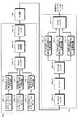
【0094】
図19は、スライスの数を3とした場合の9ビット加算器の構成を示す。さらに、この方式によるコンフィギュレーションデータのべースバンドにおける伝送系の一例および他の例を図20と図21に示す。伝送系は、コンフィギュレーションデータを無線伝送する送信機(18a,19a)、伝送路(18b,19b)、コンフィギュレーションデータを受信する受信機(18c,19c)から構成される。各受信機においてシンボルタイミング同期部、キャリア周波数同期部、伝送路等化部等の記述は省略している。
【0095】
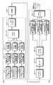
図20に示す構成において、送信機(18a)においては、表3と対応させて、スライス1、スライス2、...、スライスk(例えば(k=3))に属するLUTのコンフィギュレーションデータが格納されているメモリ(18a-1,18a-2,18a-3)からそれぞれデータがQPSK変調器(18a-4)、8PSK変調器(18a-5)、64QAM変調器(18a-6)に供給される。変調器出力信号がマルチプレクサ(18a-7)によって結合されてロールオフフィルタ(18a-8)によって占有帯域が制限された後に伝送路(18b)に送信される。
【0096】
受信側においては、受信データがロールオフフィルタ(18c-1)において帯域制限された後にサンプラー(18c-2)でシンボル周期でサンプリングを行う。サンプラー(18c-2)の出力がデマルチプレクサ(18c-3)に供給される。デマルチプレクサ(18c-3)によって変調信号が対応するQPSK復調器(18c-4)、8PSK復調器(18c-5)、64QAM復調器(18c-6)に分配される。各復調器で復調されたビットはマルチプレクサ(18c-7)によって結合されてコンフィギュレーションデータとして出力される。
【0097】
図21に示す他の例でも同様に、表4の割り当て手法にしたがって各スライスに属するLUTのコンフィギュレーションデータが対応した誤り訂正符号化方式によって符号化される。QPSK変調方式を例として挙げている。送信機(19a)においては、スライス1、スライス2、スライス3に属するLUTのコンフィギュレーションデータが格納されているメモリ(19a-1,19a-2,19a-3)からそれぞれデータが符号化率=1/3 の誤り訂正符号符号化器(19a-4)、符号化率=1/2 の誤り訂正符号符号化器(19a-5)、符号化率=3/4 の誤り訂正符号符号化器(19a-6)に供給される。符号化出力信号がマルチプレクサ(19a-7)によって結合されてQPSK変調器(19a-8)によって変調される。変調出力がロールオフフィルタ(19a-8)によって占有帯域が制限された後に伝送路(19b)に送信される。
【0098】
受信側においては、受信データがロールオフフィルタ(19c-1)において帯域制限された後にサンプラー(19c-2)でシンボル周期でサンプリングを行う。サンプラー(19c-2)の出力がデマルチプレクサ(19c-3)に供給される。デマルチプレクサ(19c-3)によって分離された信号が対応する符号化率=1/3 の誤り訂正符号復号化器(19a-4)、符号化率=1/2 の誤り訂正符号復号化器(19a-5)、符号化率=3/4の誤り訂正符号復号化器(19a-6)に供給される。なお、硬判定の復号を行う場合は、サンプラー(19c-2)とデマルチプレクサ(19c-3)の間にQPSK復調器が挿入され、ビットに復調した後に復号化器に分配されて復号が行われる。各復号化器で復号されたビットはマルチプレクサ(19c-7)によって結合されてコンフィギュレーションデータとして出力される。
【0099】
上述した第1の実施形態(すなわち、異なる変調方式の使用)、第2の実施形態(異なる誤り訂正符号の使用)、第3の実施形態(異なるシンボルレートを使用)の2以上を組み合わせるようにしても良い。
【0100】
例えば、下記の表5に示すように、重みが最大のMSBを含むスライスに属するLUTのコンフィギュレーションデータの誤り訂正符号化方式と変調方式には、それぞれ、最も誤り訂正能力の高い符号化率=1/3の符号化方式と最も伝送特性の優れたBPSK変調方式を組み合わせて伝送する。LSBを含むスライスに属するLUTのコンフィギュレーションデータに対しては、誤り訂正能力の劣るが符号化率の比較的高い符号化率=3/4の符号化方式と伝送特性は劣るが伝送効率の良い64QAM変調方式とを組み合わせて伝送する。
【0101】
【表5】
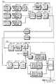
図22は、第1および第2の実施形態を組み合わせた第4の実施形態におけるコンフィギュレーションデータの伝送系の構成を示す。伝送系は、コンフィギュレーションデータを無線伝送する送信機(20a)、伝送路(20b)、コンフィギュレーションデータを受信する受信機(20c)から構成される。受信機(20a)においてシンボルタイミング同期部、キャリア周波数同期部、伝送路等化部等の記述は省略している。送信機(20a)においては、表3と対応させて、スライス1、スライス2、スライス3に属するLUTのコンフィギュレーションデータがメモリ(20a-1,20a-2,20a-3)から異なる符号化率の誤り訂正符号符号化器(20a-4,20a-5,...,20a-6)に与えられる。符号化された各スライスのコンフィギュレーションデータは対応したBPSK変調器(20a-7)、QPSK変調器(20a-8)、64QAM変調器(20a-9)によって変調が行われる。変調器出力信号はマルチプレクサ(20a-10)によって結合されてロールオフフィルタ(20a-11)によって帯域が制限された後に伝送路(20b)に送信される。
【0103】
受信側においては、ロールオフフィルタ(20c-1)において帯域制限された後にサンプラー(20c-2)でシンボル周期毎にサンプルされ、デマルチプレクサ(20c-3)によって各シンボルが対応する誤り訂正の復号化器に分配される。例えば、符号化率=1/3の復号化器(20c-4)、符号化率=1/2の復号化器(20c-5)、符号化率=3/4の復号化器(20c-6)に分配される。図22では復号化器は軟判定を行うと仮定している。なお、硬判定の復号を行う場合はデマルチプレクサとそれぞれの復号化器の間にBPSK復調器、QPSK復調器、64QAM復調器が挿入され、ビットに復調した後に復号化器に分配されて復号が行われる。各符号化器で復号されたビットはマルチプレクサ(20c-7)によって結合されてコンフィギュレーションデータとして出力される。
【0104】
さらに、信号点の配置手法を使用したこの発明の第5の実施形態について説明する。比較的多値数の多い変調方式、例えば、16QAMであれば、1シンボルで4ビットの情報を同時に伝送できるが、4ビットの組み合わせにおいて特定ビット位置のビットの伝送特性が全体のビットの平均伝送特性と比較して優れていることに着目して、スライスされたコンフィギュレーションビットを変調する際にスライスの優先順位とビット位置を考慮して信号点上でのビットの割り当てを行う。
【0105】
図23は、16QAMの信号点配置とシンボルあたり伝送可能な4ビットのビット組み合わせ(abcd)を示す。(abcd)のa,b,c,dはビットを表す。図23の信号点配置において、ビットのaとcは象限が同じであれば信号点にかかわらず同じ値である。すなわち、この位置のビットは、信号点に雑音が重畳されて他の象限に移動して誤って認識された場合のみにビット誤りが発生する。したがって、その伝送特性が16QAMの平均誤り率と比較すれば優れていると考えられる。そこで、優先順位の高いMSBスライスに属するLUTのコンフィギュレーションデータはaとcに割り当てて、LSBスライスに属するLUTのコンフィギュレーションデータはbとdに割り当てて16QAM変調を行う。この場合は全コンフィギュレーションデータを16QAMで伝送するため、9ビット加算器の場合、(384/4=96)シンボルとなる。
【0106】
第5の実施形態におけるコンフィギュレーションデータのべースバンドにおける伝送系を図24に示す。伝送系は、コンフィギュレーションデータを無線伝送する送信機(22a)、伝送路(22b)、コンフィギュレーションデータを受信する受信機(22c)から構成される。受信機(22c)においてシンボルタイミング同期部、キャリア周波数同期部、伝送路等化部等の記述は省略している。MSBスライスおよびLSBスライス側に属するLUTのコンフィギュレーションデータがメモリ(22a-1,22a-2)からそれぞれデータがビット割り当て部(22a-3)に供給され、MSBスライスのデータのビットが図23のa,cのビット位置に、LSBスライスのビットがb,dのビット位置に割り当てられる。16QAM変調器(22a-4)で変調された信号がロールオフフィルタ(22a-5)によって帯域制限が行われた後に伝送路(22b)へ送信される。
【0107】
受信側ではロールオフフィルタ(22c-1)によって帯域を制限した後にサンプラー(22c-2)によってシンボル周期でサンプリングを行い、16QAM復調器(22c-3)によって復調されたビットはa,cのビット位置のビットとb,dのビット位置のビットとに一旦分けられて、マルチプレクサ(22c-5)において結合されてコンフィギュレーションデータとして出力される。
【0108】
次に第6の実施形態について説明する。第6の実施形態は、上述した複数の方式の何れかまたは組み合わせに対して、CRCによる再送方式を組み合わせた伝送方式である。前述した第1〜第5の実施形態では、ビットに重みを有するデータを処理する演算回路を構成するコンフィギュレーションデータに対する伝送方式であった。ある回路を構成するためのコンフィギュレーションデータのエラーによって、その装置に致命的な故障が発生する場合は、そのコンフィギュレーションデータの伝送に限っては、CRCによる再送処理を併用して信頼性を高めるようになされる。
【0109】
対象となる回路としては、クロックの分周・分配回路、制御回路、CLB間の接続を決定するPMS,CLB内のマルチプレクサ、並びにビット単位で論理演算を行い、高い信頼性が要求される誤り訂正符号の符号化または復号化回路等が挙げられる。これらの回路のコンフィギュレーションデータに対しては、誤り訂正符号による符号化とCRCを併用してデータ伝送の信頼性を向上させる。対象となるコンフィギュレーションデータをCRC用コンフィギュレーションデータとよぶことにする。
【0110】
図25は、第6の実施形態によるコンフィギュレーションデータのべースバンドにおける伝送系を示す。伝送系は、コンフィギュレーションデータを無線伝送する送信機(23a)、伝送路(23b-1,23b-2)、コンフィギュレーションデータを受信する受信機(23c)から構成される。受信機(23c)においてシンボルタイミング同期部、キャリア周波数同期部、伝送路等化部等の記述は省略している。コンフィギュレーションデータの変調方式としてQPSK変調を仮定している。また、パケット生成のためのプリアンブル付加部等は省略されている。
【0111】
送信機(23a)においては、伝送すべきコンフィギュレーションデータは、CRC用コンフィギュレーションデータ(23a-1)と、スライスの数を2と仮定して、MSBスライス(23a-2)と、LSBスライスのコンフィギュレーションデータ(23a-3)とする。CRC用コンフィギュレーションデータ(23a-1)は、最も誤り訂正能力の高い符号化率=1/3の符号化器(23a-4)によって符号化された後にCRC用の符号化器(23a-5)によってCRCが付加される。他のMSBスライスとLSBスライスに属するLUTのコンフィギュレーションデータは、符号化率がそれぞれ1/2と3/4の符号化器(23a-6,23a-7)で符号化される。符号化器(23a-5)、符号化器(23a-6)および符号化器(23a-7)の出力がマルチプレクサ(23a-8)に入力され、データが結合された後にQPSK変調器(23a-9)で変調され、ロールオフフィルタ(23a-10)で帯域制限が行われて伝送路(23b-1)に送信される。
【0112】
受信側ではロールオフフィルタ(23c-1)によって帯域制限が行われて、サンプラー(23c-2)によってシンボル周期でサンプリングを行う。デマルチプレクサ(23c-3)では、CRCが付加されたコンフィギュレーションデータと、CRCが付加されていないコンフィギュレーションデータに分解される。CRCが付加された変調信号に対しては一旦QPSK復調器(23c-4)で復調されたビットに対してエラー検出部(23c-5)においてCRCによって誤りビットの検出を行う。エラーが検出されなければ、スイッチ(23c-6)が閉じられて符号化率が1/3の軟判定型の誤り訂正復号化器(23c-7)に入力されて復号が行われる。
【0113】
エラー検出部(23c-5)においてCRC用コンフィギュレーションデータに誤りビットが検出されない場合は、ACK(Acknow1edge)信号を発生して変調器(23c-8)で変調した信号をロールオフフィルタ(23c-9)、伝送路(23b-2)を介してコンフィギュレーションデータ送信側(23a)の受信部のロールオフフィルタ(23a-11)に供給される。ロールオフフィルタ(23a-11)の出力が制御信号復調器(23a-12)で復調される。ACK信号の復調後にマルチプレクサ(23a-8)が制御され、次のMSBとLSBスライスのコンフィギュレーションデータの送信を行う。コンフィギュレーションデータ受信側では受信したMSBとLSBスライスのコンフィギュレーションデータ信号に対してもデマルチプレクサによってそれぞれ、符号化率が1/2と3/4の軟判定型復号化器(23c-10,23c-11)によって復号が行われてマルチプレクサ(23c-12)で結合されてコンフィギュレーションデータとして出力される。
【0114】
エラー検出部(23c-5)においてCRC用コンフィギュレーションデータに誤りビットが検出された場合はARQ(Automatic repeat request)信号を発生して送信後に、コンフィギュレーションデータ供給側の制御信号復調器(23a-12)で復調してマルチプレクサ(23a-8)を制御してCRC用コンフィギュレーションデータの再送を行う。
【0115】
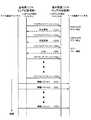
図26は、第6の実施形態によるソフトウェアパケット(24a-1,24a-2,...,24a-k)と情報パケット(24b-1,24b-2,...,24b-n)の構成例を示す。ソフトウェアパケット1は、再送処理を考慮したパケットである。プリアンブル(24c)と誤り訂正符号によって符号化されたソフトウェアデータ(24d)から構成される。ソフトウェアデータは、CRC(24e)とCRC用コンフィギュレーションデータ(24f)から構成される。MSB・LSBスライスのコンフィギュレーションデータは、ソフトウェアパケット2以降のソフトウェアパケットで伝送される。これらのパケットはプリアンブル(24g)とソフトウェアデータ(24h)から構成される。ソフトウェアデータは誤り訂正符号によって符号化されたMSB・LSBスライスのコンフィギュレーションデータパケット(24i)から構成される。情報パケットに関しては図2と同様のデータ構成とされている。
【0116】
図27は、第6の実施形態によるソフトウェア伝送パケットの再送処理シーケンスの例を示す。ソフトウェアを供給する基地局より送信されたソフトウェアパケット1(25a)に対してCRCによるエラー検出が行われてエラーが検出されれば再送要求信号(25b)を基地局に送信する。それに応じてソフトウェアパケット1(25c)を再送する。これをエラーフリーが確認されるまで繰り返す。エラーフリーが確認されたらACK信号(25f)を基地局に送信する。基地局はACK信号を受信後にソフトウェアパケット2(25g)を送信する。これはCRCによるエラー検出が行われずに、ソフトウェアパケットk(25h)まで続けて伝送される。全ソフトウェアを復調後にプログラム可能な変復調器にダウンロードされて情報パケットに対する変復調処理の設定を行う。その後に情報パケット1−n(25i,25j,...,25k)が伝送される。
【0117】
この発明は、上述したこの発明の一実施形態に限定されるものではなく、この発明の要旨を逸脱しない範囲内で様々な変形や応用が可能である。例えばMSBスライスとLSBスライスに対する変調方式としては、上述した第1の実施形態におけるQPSKと16QAMの組み合わせに限定されるものではなく、[表6]に示すような種々の組み合わせが可能である。ここでは、二つのスライスに対して適用される例を挙げているが、3以上のスライスに対して適用可能な変調方式の組み合わせも種々可能である。
【0118】
【表6】
この発明において、プログラム可能な論理回路としては、FPGA以外のデバイスを使用しても良い。また、プログラムを伝送する方法としては、無線伝送路に限定されるものではなく、有線であっても良い。
【0120】
【発明の効果】
上述したこの発明では、演算回路の入出力データバスのビットに付けられた重みの大きさによって、コンフィギュレーションデータをグループ化して各グループ(スライス)のコンフィギュレーションデータに対して、伝送特性と伝送効率の異なる変調方式、誤り訂正能力と符号化率の異なる符号化方式、またはシンボルレートの異なる伝送方式を適用して伝送している。この発明によれば、伝送されたコンフィギュレーションデータによってプログラムされた変復調器の伝送品質に著しい劣化を来さずに、コンフィギュレーションデータの伝送時間を短縮できる。さらに、この発明によれば、多値数の比較的多い16QAMのような変調方式において各スライスのコンフィギュレーションビットを伝送特性の異なるビット位置に割り当て伝送するので、等しい伝送時問で伝送されたコンフィギュレーションデータによってプログラムされた変復調器の伝送品質を向上させることができる。
【図面の簡単な説明】
【図1】この発明を適用できるソフトウェア無線通信装置の一例を示すブロック図である。
【図2】ソフトウェア無線通信システム用のソフトウェアをダウンロードするリンクのパケットの構成例、並びに情報データを伝送するリンクのパケットの構成例を示す略線図である。
【図3】ソフトウェア無線通信システムにおいて端末局から基地局に対して伝送するデータのパケットの構成例を示す略線図である。
【図4】パケットの再送処理を示す略線図である。
【図5】MMAC用のOFDM復調部の構成例を示すブロック図である。
【図6】WCDMA用のスペクトラム拡散方式復調部の構成例を示すブロック図である。
【図7】FPGA内部の構成例を示すブロック図である。
【図8】CLB内部の構成例を示すブロック図である。
【図9】FPGAのLUTとCLで設計した9ビット加算器の構成例を示すブロック図である。
【図10】FPGAのLUTとCLで設計した3×2ビットの乗算器の構成例を示すブロック図である。
【図11】FPGAのLUTで設計した演算回路の構成例を示すブロック図である。
【図12】9ビット加算器におけるスライス分割を示すブロック図である。
【図13】3×2ビット乗算器におけるスライス分割を示すブロック図である。
【図14】2入力演算回路におけるスライス分割を示すブロック図である。
【図15】2入力演算回路におけるスライス分割を示すブロック図である。
【図16】この発明の第1の実施形態におけるコンフィギュレーションデータの伝送系を示すブロック図である。
【図17】この発明の第2の実施形態におけるコンフィギュレーションデータの伝送系を示すブロック図である。
【図18】この発明の第3の実施形態におけるコンフィギュレーションデータの伝送系を示すブロック図である。
【図19】スライス分割数を3とした9ビット加算器の構成を示すブロック図である。
【図20】スライス分割数を3とした場合のコンフィギュレーションデータの伝送系の一例を示すブロック図である。
【図21】スライス分割数を3とした場合のコンフィギュレーションデータの伝送系の他の例を示すブロック図である。
【図22】この発明の第4の実施形態におけるコンフィギュレーションデータの伝送系を示すブロック図である。
【図23】16QAMの信号点配置とシンボルあたり伝送可能な4ビットのビット組み合わせを示す略線図である。
【図24】この発明の第5の実施形態におけるコンフィギュレーションデータの伝送系を示すブロック図である。
【図25】この発明の第6の実施形態におけるコンフィギュレーションデータの伝送系を示すブロック図である。
【図26】この発明の第6の実施形態におけるソフトウェアパケットの構成例を示す略線図である。
【図27】この発明の第6の実施形態におけるソフトウェアパケットの再送処理シーケンスの例を示す略線図である。
【符号の説明】
1p・・・デマルチプレクサ、1o・・・ソフトウェア変調信号復調部、1q・・・ソフトウェアメモリ、1r・・・ソフトウェア変調部、15a・・・送信機、15b・・・伝送路、15c・・・受信機、15a-3・・・QPSK変調器、15a-4・・・16QAM変調器[0001]
BACKGROUND OF THE INVENTION
The present invention relates to a radio communication apparatus, a program transmission apparatus and method thereof, and a radio communication system using software radio technology.
[0002]
[Prior art]
Recently, software defined radio is being developed. Software defined radio is a concept for a system in which basic radio functions (bandwidth, filtering, modulation / demodulation, encoding, etc.) can be changed by software. Features of software defined radio include reconfigurability (change in configuration and specifications) and downloadability (program rewritability). A radio configured with software defined radio technology is called a software defined radio. More specifically, in the software radio communication technology, a programmable modulation / demodulation device for digital radio communication is configured by using a microprocessor, a DSP (Digital Signal Processor) chip or an FPGA (Field Programmable Gate Array), and desired communication is performed. Software for configuring the modulation / demodulation method can be downloaded to the modulation / demodulation device by wire or wirelessly, and various uses can be flexibly realized with the same hardware.
[0003]
For example, if different wireless communication systems such as PHS (Personal Handyphone System), mobile phone, and local area network (LAN) can be realized by one wireless communication device by downloading software, the user can use the same wireless terminal. As long as you have the equipment, you can get service all over the world by downloading the local communication system program. For the manufacturer of the terminal device, mass production is possible by sharing the hardware, and the manufacturing cost can be reduced. Further, since the function of the wireless communication apparatus can be easily updated, it is easy for the communication carrier to add a new service, upgrade the function, change the system, correct a software error, and the like. In addition, by downloading software via radio, the bit rate, modulation / demodulation method, error correction coding / decoding method, etc. can be flexibly set according to the propagation environment, providing optimal transmission quality for the propagation environment and subscribers. Allows an increase in number.
[0004]
FIG. 1 shows an example of a software defined radio apparatus to which the present invention can be applied. The signal having the center frequency fc received from the antenna (1a) passes through the antenna switch (1b) and is input to the low noise amplifier (1j). The signal output from the low noise amplifier is mixed with the oscillation frequency f11 of the first local oscillator (1c) in the reception mixer (1k) and converted to a signal of the intermediate frequency fi.
[0005]
The signal converted to the intermediate frequency fi is subjected to quadrature detection at the quadrature detector (1l) by the intermediate frequency f12 of the second local oscillator (1d) and converted to analog baseband signals I and Q. The analog baseband signals I and Q are converted into digital baseband signals ID and QD by an A / D converter (1m). Digital baseband signals ID and Q-D are supplied to a demultiplexer (1p).
[0006]
The demultiplexer (1p) selects a software transmission packet or an information data transmission packet. At the time of software download, the output data ID and Q-D of the A / D converter are demodulated by the software modulation signal demodulator (1o). The demodulated program is downloaded to the programmable baseband digital modulation unit (1i) or the programmable baseband digital demodulation unit (1n). After downloading, the demultiplexer (1p) supplies the output data ID and Q-D of the A / D converter to the programmable baseband digital demodulator (1n), and the desired demodulation processing determined by the program is performed. Done.
[0007]
As an example, the programmable baseband digital modulation unit (1i) and the programmable baseband digital demodulation unit (1n) can be programmed according to a program from the software modulation signal demodulation unit (1o). Multiplex) modulation and demodulation functions and W-CDMA (Wideband-CDMA: Wideband code division multiple access) modulation and demodulation functions can be switched. This modulation / demodulation method is an example of a multi-mode wireless device, and the present invention may implement a GSM (Global System for Mobile Communication) in a program. Furthermore, the present invention is not limited to mobile communication, but can be applied to different systems in wireless LAN, different systems in ITS (Intelligent Transport System), and the like.
[0008]
When transmitting the software to be downloaded to the other station, the software stored in the software memory (1q) is modulated by the software modulation section (1r), and the digital IQ signals I-D, Q passed through the multiplexer (1s) -D is input to the D / A converter (1h). The D / A converter (1h) converts the digital IQ signal into an analog signal. When transmitting information bits, the modulated data bits are modulated with a desired modulation scheme by a programmable baseband digital modulator (1i). The output of the modulation unit (1i) passes through the multiplexer (1s) and is input to the D / A converter (1h) as digital baseband signals ID and Q-D. Note that the software memory (1q) and the software modulation unit (1r) are not limited to the base station, but may be included in the terminal station.
[0009]
The analog signal is quadrature modulated in the quadrature modulator (1g) by the oscillation frequency f12 of the second local oscillator (1d) and converted to a signal having an intermediate frequency fi (= f12). The signal modulated to the intermediate frequency fi is converted into a signal of frequency fc (= f12 + f11) by the frequency f11 of the first local oscillator (1c) in the transmission mixer (1f).
[0010]
The OFDM modulated signal converted to the frequency fc is amplified to a predetermined transmission power in the power amplifier (1e). The amplified signal is supplied to the antenna (1a) via the antenna switch (1b) and transmitted. In mobile radio communications using a broadband spectrum such as MMAC (Mu1timedia mobi1e accesscommunication system) and WCDMA (Wideband code division mu1tip1e access), the A / D converter (1m) and the D / A converter (1h) The sampling frequency is several tens of MSPS (Mega samples per second).
[0011]
FIG. 2 shows a configuration example of a link packet for wirelessly downloading software for a software defined radio communication system and a configuration example of a link packet for transmitting information data. This link is a downlink from the base station to the terminal station. Packets are software packets (2a-1,2a-2, ..., 2a-k) and information packets (2b-1,2b-2, ..., 2b-n) that transmit information data Consists of
[0012]
The software packet is composed of a preamble (2c) and software (2d). The software (2d) includes data (2e) for CRC (Cyc1ic redundancy check) added for error detection, and configuration data for reconfiguring a program or FPGA to be input to the microprocessor (or DSP). 2f). The information packet is composed of a preamble (2g) and information symbols (2h-1, 2h-2, ..., 2h-m).
[0013]
A preamble that is a known signal is detected for the received data, and packet timing synchronization, frequency synchronization, and transmission path equalization are performed based on the detection. For received software, error detection is performed by CRC. If an error is detected, the packet is discarded and retransmission is requested. Only when no error is detected, the program is demodulated and an ACK signal (acknowledge signal) is transmitted to prompt transmission of the next packet. When all the programs are demodulated, the demodulated programs are downloaded to the baseband digital signal modulation unit (1i) and the demodulation unit (1n) and set to a desired modulation / demodulation method. After receiving the information packet and performing packet timing synchronization, frequency synchronization, transmission path equalization on the preamble (2g), information packet information symbols (2h-1,2h-2, ..., 2h-m) The data is demodulated by the demodulation method set for.
[0014]
FIG. 3 shows a configuration example of a link (uplink) packet transmitted from a terminal station to a base station by a modulation unit in which software is downloaded in a software defined radio communication system. Packets (3a-1, 3a-2,..., 3a-n) are composed of a preamble (3b) which is a known signal and information data (3c). Information data (3c) is composed of information symbols (3d-1, 3d-2,..., 3d-m). On the receiving side, packet timing synchronization, frequency synchronization, and transmission path equalization are performed based on the detection of the preamble, and then information symbols are demodulated.
[0015]
FIG. 4 shows an example of packet retransmission processing in the software defined radio communication system. In a software radio communication system, modulation / demodulation of information data to be originally transmitted is performed by a modulation / demodulation unit downloaded with software. There is a possibility that a failure occurs in the modem unit due to a software error generated by the wireless transmission path. Therefore, error detection by CRC is performed on the software radio transmission packet, and retransmission processing is performed many times until error free (no error).
[0016]
For example, the first software packet 1 (4a) is transmitted from the software transmitting station. Error detection by CRC is performed on the received packet, and if an error is detected, a retransmission request signal (4b) is transmitted to the transmitting station until no error is detected. Since FIG. 4 shows an example in which error is not caused by software packet 1 (4e) transmitted after two retransmission requests are made, the same packet (4a, 4c, 4e) is retransmitted three times. After error free, the ACK signal (4f) is transmitted to the software transmission side.
[0017]
After repeating these operations, the final software packet k (4k) is received, and the demodulation of all the software is completed. The decoded software is downloaded to a programmable modem unit, and a desired modulation / demodulation process can be performed. After transmitting the ACK signal (41) for the final software packet k (4k), the information packets (4m, 4n,..., 4o) are transmitted.
[0018]
Next, processing contents of the programmable baseband digital demodulator (1n) in FIG. 1 will be described. Since the processing of the demodulation unit is generally more complicated than the modulation unit, only the demodulation unit will be described. As an example, a configuration of a demodulating unit of MMAC and WCDMA, which are mobile radio communication systems using a broadband spectrum, will be described.
[0019]
FIG. 5 shows a configuration example of an OFDM demodulator for MMAC. The input digital baseband signals ID and Q-D are obtained by first obtaining the packet timing synchronization by the packet timing synchronization unit (5a) and then synchronizing the carrier frequency by the carrier frequency synchronization unit (5b). After the data is written in (5c), it is transformed into the frequency domain by FFT (fast Fourier transform) (5d). If the number of subcarriers is NFFT, fast Fourier transform of the NFFT point is performed in FFT (5d), that is, demodulated into parallel received data at the NFFT point. Thereafter, the equalizer (5e) performs channel equalization, and the error correction code decoder (5f) corrects the error bit and outputs it as a demodulated bit.
[0020]
FIG. 6 shows a configuration example of a spread spectrum demodulation unit for WCDMA. The input digital baseband signals ID and Q-D first obtain packet timing synchronization by the packet timing synchronization unit (6a), and then synchronize the carrier frequency by the carrier frequency synchronization unit (6b). After the data is written in the memory (6c), the despreading and equalization unit (6d) performs despreading and transmission path equalization using a predetermined spreading code. The output of the despreading / equalizing unit (6d) is supplied to the error correction code decoder (6e), the error bit is corrected by the decoder (6e), and the demodulated bit is output.
[0021]
In the demodulator as shown in FIG. 5 and FIG. 6 described above, it is necessary to perform processing such as FFT, despreading, and equalizer on the sampling data input at a rate of several tens of MSPS in real time. is there. In a software defined radio communication system, these processes are realized by programmable hardware. The use of an ultra-high-speed general-purpose microprocessor that operates with a clock of several hundred MHz as a programmable device is also conceivable. However, since the power consumption depends on the clock frequency, it is difficult to design a practical portable information terminal device that operates on a battery.
[0022]
By using an FPGA as a programmable device, signal processing hardware for high-speed demodulation with relatively low power consumption can be realized. Since a large-scale FPGA exceeding 1 million gates has started to appear on the market, the function of an OFDM LSI for MMAC exceeding 1.4 million gates can be sufficiently realized by using several FPGAs. However, in order to program the FPGA to a desired function, configuration data for programming the function of the reconfigurable logic circuit inside the FPGA and the connection between the logic circuits is required. In order to program the above-described MMAC OFDM LSI, 8 Mbits of configuration data are required.
[0023]
In this description, the term “software” or “program” also includes configuration data that defines the functionality of the FPGA.
[0024]
The FPGA constituting the baseband processing unit will be described. FIG. 7 shows the internal configuration of the FPGA. First, configuration data is supplied from the outside to the FPGA chip (7a) and written to the configuration memory (7c). The function of the circuit of each part is programmed by this data.
[0025]
A CLB (Configurab1e 1ogic b1ock) (7g), which is a programmable logic circuit block, can be configured into a small-scale logic circuit desired by the user by corresponding configuration data. An IOB (Input / output b1ocks) (7d) is an interface circuit for signals outside and inside the chip, and is also a kind of current amplifier. A predetermined logic amplitude voltage is set by corresponding configuration data and has a function of converting an external logic voltage into an internal logic voltage. RC (Routing channel 1) (7e) is a data bus for connecting the blocks, and data transfer is performed between CLBs and IOBs or between CLB and IOBs. PSM (Programmab1e switch matrix) (7f) and CB (Connection Block) (7h), which are programmable switches, are arranged in a matrix and set the connection between RCs according to the corresponding configuration data. Data can be exchanged on the Internet.
[0026]
FIG. 8 shows an internal configuration example of the CLB. CLB is a 4-input 1-output LUT (Look-up tab1e) (8a, 8b), a 3-input 1-output LUT (8c), and CL (Carry 1ogic), a programmable logic circuit dedicated to carry generation. 8d, 8e), 9 multiplexers (8f, 8g, 8h, 8i, 8j, 8k, 81, 8m, 8n) and 2 registers (8o, 8p). CLB is SRAM, and input corresponds to an address. Arbitrary logic circuits can be configured by downloading 16-bit and 8-bit configuration data for 4-input and 3-input CLB, respectively. Table 1 shows an example of a truth table for a 4-input LUT.
[0027]
[Table 1]
The CL can realize one of several logic circuits defined in advance by corresponding configuration data. The control signal for each multiplexer is also set by the configuration data. By applying various configuration data to the CLB, a desired logic circuit including a register can be realized.
[0029]
As described above, by supplying configuration data from the configuration memory shown in FIG. 7 to the IOB, PSM, CB, and CLB, a logic circuit having a desired specification can be realized by the FPGA.
[0030]
An adder, a multiplier, and an arbitrary two-input arithmetic circuit designed using the FPGA block will be described below. In order to simplify the description, the contents of the LUT and the CL setting data will be referred to as configuration data unless otherwise specified.
[0031]
FIG. 9 shows a configuration example of a 9-bit adder designed by FPGA LUT and CL. This is a ripple carry type adder in which a carry signal propagates from a lower bit. The bits a8-a0 and b8-b0 of the input data bus expressed in two's complement are first converted into LUTs (9a-1, 9a-2, 9a-3, 9a-4, 9a-5, 9a-6, 9a -7, 9a-8, 9a-9, 9a-10). The LUT (9a-1) generates a control signal indicating that an overflow has occurred. Other LUTs calculate the sum of two bits of equal weight and the carry signal from the lower bits.
[0032]
CL (9b-1, 9b-2, 9b-3, 9b-4, 9b-5, 9b-6) is the generation of the carry signal in each bit corresponding to the input data bus and the digit from the lower bit to the upper bit. Propagate signal. In the final stage LUT (9c-1, 9c-2, 9c-3, 9c-4, 9c-5, 9c-6, 9c-7, 9c-8), code processing corresponding to the two's complement representation for the sum output And saturation processing at overflow. In addition to this example, various adder algorithms have been proposed.
[0033]
FIG. 10 shows a configuration example of a 3 × 2 bit multiplier designed using the LUT and CL of the FPGA. The input data a2, a1, a0 and b1, b0 expressed in two's complement form the corresponding LUT (10a-1, 10a-2, 10a-3), LUT (10a-5, 10a-6) and CL, respectively. It is converted into an absolute value by (10b-1, 10b-2, 10b-3). The sign of the product is determined by LUT (1Oa-4). The bits a′2, a′1, a0 ′ and b′1, b′0 of the absolute value are supplied to the LUT (10c-1, 10c-2,..., 10c-6), and the LUT (10c− 1,10c-2, ..., 10c-6) calculate the partial product. Partial products are LUT (10d-1,10d-2,10d-3), CL (1Oe-1,10e-2), LUT (10f-1,10f-2, ..., 10f-5) and CL ( The products are calculated by addition with an addition tree composed of 10g-1, 10g-2, 10g-3, 10g-4).
[0034]
An arbitrary 2-input arithmetic circuit is designed by the LUT. Table 2 shows an example of a truth table of a 2-input 1-output arithmetic circuit whose data word length is 12 bits as [Table 2].
[0035]
[Table 2]
FIG. 11 shows a configuration example of an arithmetic circuit designed by LUT based on this truth table. Since the total number of bits of input data is 24 bits, this can be realized by preparing 12 logic circuits with 24 inputs and 1 output. The output bits c11 (MSB), c10,..., C0 (LSB) are connected to the logic circuit (1111 , 11Ten , ..., 110 ). Each logic circuit is composed of eight LUTs (11a-1, 11a-2, 11a-3, 11a-4, 11a-5, 11a-6, 11a-7, 11a-8) for inputting 24-bit data. Composed.
[0037]
Configuration data is written in each LUT of each logic circuit so as to satisfy the truth table (Table 2). The configuration shown in FIG. 11 is an example in which the number of LUTs is maximum because the LUTs are designed by connecting them directly in a tree shape. Depending on the contents of the truth table, it is possible to reduce the number of LUTs by simplifying the logical expression.
[0038]
The timing synchronization unit (5a, 6a), carrier frequency synchronization unit (5b, 6b), FFT (5d), despreading / equalization unit (6d) shown in FIGS. In the process of OFDM transmission line equalization (5e), division is performed. That is, a multiplier, an adder, and a divider are required to configure the processing circuit on the FPGA. Input data is input at a sampling rate of several tens of MHz and needs to be calculated in real time. Assuming that the operation time of the operation circuit composed of the FPGA LUT and CL is several tens of nsec, it is difficult to share the hardware in a time-sharing manner, and each operation unit needs its own operation circuit. It becomes. Therefore, a large number of LUTs and CLs are required to configure the entire baseband modulation / demodulation process. For example, in order to realize only MMAC FFT on an FPGA, as many CLs as 2300 LUTs are required. A large amount of configuration data is required to program them. Further, since the OFDM modulation / demodulation LSI for MMAC has a scale of 1.4 million gates or more, if it is assumed to be configured with an FPGA, configuration data of 8 Mbits or more is required.
[0039]
[Problems to be solved by the invention]
As shown in FIG. 4, in the conventional software wireless download method, CRC is performed on the received software, and after error-free is confirmed, downloading to the programmable device is performed. If an error is detected, a retransmission request is made until error free. In this method, under a poor propagation environment, it is necessary to retransmit an enormous amount of configuration data many times until reaching error-free, and enormous time is spent until the download is completed.
[0040]
If the download time of configuration data increases, the transmission efficiency of information data to be originally transmitted as shown in the packet configuration diagram of FIG. 2 deteriorates. In addition, in an adaptive transmission system that realizes an optimal function by wireless download according to a propagation path environment that changes from moment to moment, transmission of configuration data for realizing the function needs to be performed promptly. In the transmission method with re-transmission, the propagation environment changes drastically until the wireless download is completed, and a function optimal for the propagation environment after the download is completed cannot be realized on the FPGA. Therefore, in order to utilize the features of the software defined radio communication system, it is essential to establish a highly efficient radio transmission / download method for software including FPGA configuration data.
[0041]
Accordingly, an object of the present invention is to provide a radio communication apparatus, a program transmission apparatus and method, and a radio communication system capable of improving the transmission efficiency of a program such as FPGA configuration data.
[0042]
[Means for Solving the Problems]
In order to solve the above-described problems, the invention of
The logic circuit of the binary arithmetic circuit composed of programmable logic circuits is divided into at least first and second groups according to the magnitude of the power of 2 corresponding to each bit of the input / output,
The first program for the logic circuit of the first group having a large weight is transmitted after being modulated by the first method with few bit errors, and the program for the logic circuit of the second group having a small weight is excellent in transmission efficiency. 2 is a wireless communication apparatus that is modulated and transmitted in accordance with the second method.
[0043]
According to a third aspect of the present invention, there is provided a wireless communication apparatus in which a part or all of hardware is configured by a programmable logic circuit, and a desired wireless communication system is realized by receiving a program for the logic circuit.
The logic circuit of the binary arithmetic circuit composed of programmable logic circuits is divided into at least first and second groups according to the magnitude of the power of 2 corresponding to each bit of the input / output,
The first program for the logic circuit of the first group having a large weight is transmitted using an encoding method having a high error correction capability, and the second program for the logic circuit of the second group having a small weight is encoded. This is a wireless communication apparatus that is configured to transmit using a high-rate coding method.
[0044]
According to a fourth aspect of the present invention, there is provided a wireless communication apparatus in which a part or all of hardware is configured by a programmable logic circuit, and a desired wireless communication system is realized by receiving a program for the logic circuit.
The logic circuit of the binary arithmetic circuit composed of programmable logic circuits is divided into at least first and second groups according to the magnitude of the power of 2 corresponding to each bit of the input / output,
The first program for the first group of logic circuits having a large weight is modulated and transmitted at a low symbol rate, and the program for the second group of logic circuits having a small weight is modulated and transmitted at a high symbol rate. The wireless communication apparatus is configured to be configured as described above.
[0045]
According to a fifth aspect of the present invention, there is provided a wireless communication apparatus in which a part or all of hardware is configured by a programmable logic circuit, and a desired wireless communication system is realized by receiving a program for the logic circuit.
A programmable logic circuit is divided into an arithmetic circuit and a non-arithmetic circuit, and a part of the first program for the arithmetic circuit is transmitted without being subjected to retransmission processing, and a part of the arithmetic circuit and a second part for the non-arithmetic circuit are transmitted. The program is a wireless communication device that is retransmitted to improve reliability.
[0046]
According to a seventh aspect of the present invention, there is provided a wireless communication apparatus in which a part or all of hardware is configured by a programmable logic circuit, and a desired wireless communication system is realized by receiving a program for the logic circuit.
The logic circuit of the binary arithmetic circuit composed of programmable logic circuits is divided into at least first and second groups according to the magnitude of the power of 2 corresponding to each bit of the input / output,
The first program for the logic circuit of the first group having a large weight is transmitted by a transmission method combining two or more of the first modulation method, the first error correction code, and the first symbol rate,
The second program for the second group of logic circuits having a small weight is transmitted by a transmission method combining two or more of the second modulation method, the second error correction code, and the second symbol rate,
The first modulation method has fewer errors than the second modulation method,
The first error correction code has higher error correction capability than the second error correction code,
The first symbol rate is a wireless communication device that is lower than the second symbol rate.
[0047]
The invention according to
The logic circuit of the binary arithmetic circuit composed of programmable logic circuits is divided into at least first and second groups according to the magnitude of the power of 2 corresponding to each bit of the input / output,
The first and second programs are transmitted using a relatively large number of modulation schemes;
The first group of programs having a large weight are assigned to bit positions that allow transmission superior to the average error rate of the modulation scheme, and the second group of programs having a small weight is larger than the average error rate of the modulation scheme. A wireless communication device assigned to bit positions having inferior transmission characteristics.
[0048]
According to a twelfth aspect of the present invention, there is provided a wireless communication apparatus in which a part or all of hardware is configured by a programmable logic circuit, and a desired wireless communication system is realized by receiving a program for the logic circuit. In the transmission method for transmitting the program,
The logic circuit of the binary arithmetic circuit composed of programmable logic circuits is divided into at least first and second groups according to the magnitude of the power of 2 corresponding to each bit of the input / output,
The first program for the first group of logic circuits having a large weight is modulated and transmitted by the first method with few bit errors, and the program for the second group of logic circuits having a small weight is excellent in transmission efficiency. This is a program transmitting apparatus that modulates and transmits in the manner described above. The invention of
[0049]
According to a fourteenth aspect of the present invention, there is provided a wireless communication apparatus in which a part or all of hardware is configured by a programmable logic circuit, and a desired wireless communication system is realized by receiving a program for the logic circuit. In the transmission device that transmits the program,
The logic circuit of the binary arithmetic circuit composed of programmable logic circuits is divided into at least first and second groups according to the magnitude of the power of 2 corresponding to each bit of the input / output,
The first program for the logic circuit of the first group having a large weight is transmitted using an encoding method having a high error correction capability, and the second program for the logic circuit of the second group having a small weight is encoded. This is a program transmitting apparatus that transmits data using a high coding method. The invention of
[0050]
According to a fifteenth aspect of the present invention, there is provided a radio communication apparatus in which a part or all of hardware is configured by a programmable logic circuit, and a desired radio communication system is realized by receiving a program for the logic circuit. In the transmission device that transmits the program,
The logic circuit of the binary arithmetic circuit composed of programmable logic circuits is divided into at least first and second groups according to the magnitude of the power of 2 corresponding to each bit of the input / output,
The first program for the first group of logic circuits having a large weight is modulated and transmitted at a low symbol rate, and the program for the second group of logic circuits having a small weight is modulated and transmitted at a high symbol rate. This is a program transmission apparatus. The invention of
[0051]
According to a sixteenth aspect of the present invention, there is provided a wireless communication apparatus in which a part or all of hardware is configured by a programmable logic circuit, and a desired wireless communication system is realized by receiving a program for the logic circuit. In the transmission device that transmits the program,
A programmable logic circuit is divided into an arithmetic circuit and a non-arithmetic circuit, a part of the first program for the arithmetic circuit is transmitted without being subjected to retransmission processing, and a part of the arithmetic circuit and the second program for the non-arithmetic circuit Is a program transmission device that performs retransmission processing to improve reliability. The invention of
[0052]
The invention according to claim 18 is a wireless communication apparatus in which a part or all of hardware is configured by a programmable logic circuit, and a desired wireless communication system is realized by receiving a program for the logic circuit. In the transmission device that transmits the program,
The logic circuit of the binary arithmetic circuit composed of programmable logic circuits is divided into at least first and second groups according to the magnitude of the power of 2 corresponding to each bit of the input / output,
Transmitting a first program for the logic circuit of the first group having a large weight by a transmission method combining two or more of the first modulation method, the first error correction code, and the first symbol rate;
Transmitting a second program for the logic circuit of the second group with a small weight by a transmission method combining two or more of the second modulation method, the second error correction code, and the second symbol rate;
The first modulation method has fewer errors than the second modulation method,
The first error correction code has higher error correction capability than the second error correction code,
The first symbol rate is a program transmission device that is lower than the second symbol rate. The invention of
[0053]
According to a nineteenth aspect of the present invention, there is provided a wireless communication apparatus in which a part or all of hardware is configured by a programmable logic circuit, and a desired wireless communication system is realized by receiving a program for the logic circuit. In the transmission device that transmits the program,
The logic circuit of the binary arithmetic circuit composed of programmable logic circuits is divided into at least first and second groups according to the magnitude of the power of 2 corresponding to each bit of the input / output,
The first and second programs are transmitted using a modulation scheme having a relatively large number of values, and the first group of programs having a large weight are transmitted to bit positions that can be transmitted better than the average error rate of the modulation scheme. This is a program transmitting apparatus that allocates a second group of programs having a small allocation and weight to bit positions having transmission characteristics inferior to the average error rate of the modulation scheme. The invention of
[0054]
According to a thirty-second aspect of the present invention, there is provided a wireless communication apparatus in which a part or all of hardware is configured by a programmable logic circuit, and a desired wireless communication system is realized by receiving a program for the logic circuit; In a wireless communication system including a transmission device that transmits a program to a wireless communication device,
The wireless communication apparatus has at least first and second groups in which a logic circuit of a binary arithmetic circuit composed of programmable logic circuits has at least a power of 2 corresponding to each input / output bit. Divided into
The transmission apparatus modulates and transmits the first program for the logic circuit of the first group having a large weight in the first method with a small number of bit errors, and the transmission efficiency of the program for the logic circuit of the second group having a small weight is improved. This is a wireless communication system that modulates and transmits the signal using the excellent second method.
[0055]
According to a thirty-third aspect of the present invention, there is provided a wireless communication apparatus in which a part or all of hardware is configured by a programmable logic circuit, and a desired wireless communication system is realized by receiving a program for the logic circuit; In a wireless communication system including a transmission device that transmits a program to a wireless communication device,
The wireless communication apparatus has at least first and second groups in which a logic circuit of a binary arithmetic circuit composed of programmable logic circuits has at least a power of 2 corresponding to each input / output bit. Divided into
The transmitting apparatus transmits the first program for the first group of logic circuits having a large weight using an encoding method having a high error correction capability, and the second program for the second group of logic circuits having a small weight is transmitted. The wireless communication system is configured to transmit using a coding method having a high coding rate.
[0056]
The invention of
The wireless communication apparatus has at least first and second groups in which a logic circuit of a binary arithmetic circuit composed of programmable logic circuits has at least a power of 2 corresponding to each input / output bit. Divided into
The transmitting apparatus modulates and transmits the first program for the first group of logic circuits having a large weight at a low symbol rate and modulates the program for the second group of logic circuits having a small weight at the high symbol rate. The wireless communication system is configured to transmit the data.
[0057]
The invention of claim 35 is a wireless communication apparatus in which a part or all of the hardware is configured by a programmable logic circuit, and a desired wireless communication system is realized by receiving a program for the logic circuit; In a wireless communication system including a transmission device that transmits a program to a wireless communication device,
In the wireless communication device, a programmable logic circuit is divided into an arithmetic circuit and a non-arithmetic circuit,
The transmission apparatus transmits a part of the first program for the arithmetic circuit without performing the retransmission process, and performs a part of the arithmetic circuit and the second program for the non-arithmetic circuit by performing the retransmission process to increase reliability. This is a radio communication system.
[0058]
The invention of
The wireless communication apparatus has at least first and second groups in which a logic circuit of a binary arithmetic circuit composed of programmable logic circuits has at least a power of 2 corresponding to each input / output bit. Divided into
The transmission apparatus transmits the first program for the logic circuit of the first group having a large weight by a transmission method combining two or more of the first modulation method, the first error correction code, and the first symbol rate. And
Transmitting a second program for the logic circuit of the second group with a small weight by a transmission method combining two or more of the second modulation method, the second error correction code, and the second symbol rate;
The first modulation method has fewer errors than the second modulation method,
The first error correction code has higher error correction capability than the second error correction code,
The first symbol rate is a wireless communication system in which the first symbol rate is lower than the second symbol rate.
[0059]
The invention of claim 37 is a wireless communication apparatus in which a part or all of hardware is configured by a programmable logic circuit, and a desired wireless communication system is realized by receiving a program for the logic circuit; In a wireless communication system including a transmission device that transmits a program to a wireless communication device,
The wireless communication apparatus has at least first and second groups in which a logic circuit of a binary arithmetic circuit composed of programmable logic circuits has at least a power of 2 corresponding to each input / output bit. Divided into
The transmission device transmits the first and second programs using a modulation scheme having a relatively large number of values,
The first group program having a large weight is assigned to a bit position capable of transmission superior to the average error rate of the modulation method, and the second group program having a small weight is transmitted inferior to the average error rate of the modulation method. A wireless communication system that allocates bit positions having characteristics.
[0060]
In the present invention, the transmission system of the program for the programmable logic circuit is varied depending on the importance. In other words, it is divided into those that have a large effect of program errors and those that do not, and those that have a large effect on errors are transmitted so that errors are unlikely to occur during transmission. , Transmit with emphasis on transmission efficiency.
[0061]
DETAILED DESCRIPTION OF THE INVENTION
Embodiments of the present invention will be described below. For easy understanding of the present invention, a programmable logic circuit such as an arithmetic circuit will be described first. In general, main signal processing circuits for digital wireless communication such as FFT, correlator, and digital filter are composed of an adder, a subtracter, and a multiplier based on binary arithmetic. In the FPGA, these arithmetic circuits are configured using a large number of LUTs. In an arithmetic unit based on a binary number system, each bit of the data bus is given a power of 2 power. Each bit of the data bus is connected to the input / output of the LUT.
[0062]
Error bits are generated in the configuration data transmitted wirelessly. The error bit causes an error in the operation result. The influence on the operation result differs depending on the weight attached to the bit handled by the LUT. When a 4-input 1-output LUT having 16-bit configuration data having the same number and position of error bits is connected to the LSB of the input / output bus of the arithmetic unit, the arithmetic error is small relative to the dynamic range of the data. In addition, the influence of calculation errors is small.
[0063]
However, when the LUT is connected to the MSB of the input / output bus of the arithmetic unit, the arithmetic error becomes relatively large with respect to the dynamic range of the data, so that the arithmetic error significantly affects the result. That is, the influence of the LUT configuration data error on the transmission quality of the communication device programmed with the configuration data, for example, the BER (Bit error rate) depends on which digit of the binary number the LUT containing the configuration data error has. It differs depending on whether the process is performed.
[0064]
For example, in the case of the 9-bit adder shown in FIG. 9, each bit of the input / output data bus has 2 bits for LSB to MSB.0 , 21 , 22 , 2Three , 2Four , 2Five , 26 , 27 , -28 Is weighted. If attention is paid to the LUT (9c-8) connected to the LSB of the sum output data bus and the LUT (9a-2) connected to the MSB, the same error bit occurs in the configuration data of both LUTs. The maximum value of errors that occur in the sum output data bus is 2 respectively.0 And -28 Thus, the influence of the error bits of the configuration data of the LUT (9a-2) connected to the MSB is large. If it is a part of the circuit of the demodulator, the influence on the BER is also large.
[0065]
In consideration of such points, in the present invention, the data bus of the operand of the arithmetic unit is divided into a plurality of groups. To simplify the description, the LUT connected to the data bus bits is divided into two slices. The LSB group and the CL group on the MSB side are called MSB slices, and the LUT group and the CL group on the LSB side are called LSB slices. In a broad sense, a slice includes LUT and CL configuration data. For example, if the input / output data bit weights of both slices are compared, the bit weight handled by the LUT belonging to the MSB slice is larger. Assuming that errors occur with the same probability in all LUT configuration data, the LUT belonging to the MSB slice has a larger error in the operation result than the LUT belonging to the LSB slice, and the effect of degrading the BER of the demodulator is large.
[0066]
Therefore, a transmission method with excellent transmission characteristics that hardly causes bit errors is applied to the MSB slice, while a transmission method with excellent transmission efficiency is applied to the LSB slice even though the transmission characteristics are inferior. Thus, by properly using the transmission scheme for both slices, the total number of symbols can be reduced, so that the transmission time can be reduced. Hereinafter, slice division when the present invention is applied to some of the arithmetic circuits described above will be described.
[0067]
FIG. 12 shows an example in which the LUT is divided into an MSB slice and an LSB slice for the operand input and sum output data paths in the 9-bit adder. Assume that CL configuration data is 16 bits. If the number of LUTs belonging to the MSB slice on the operand side and the sum side is 6 and 3, respectively, the number of LUTs belonging to the LSB slice is 4 and 5, respectively. Regarding CL, the number belonging to the MSB slice and the LSB slice is three. The number of bits of configuration data is a value obtained by multiplying the number of bits by 16, which is the number of bits of configuration data of LUT and CL.
[0068]
The configuration bits of the MSB slice are 12 × 16 = 192 bits, and the configuration bits of the LSB slice are 12 × 16 = 192 bits.
[0069]
FIG. 13 shows a configuration example when slice division is performed on the 3 × 2 bit multiplier shown in FIG. 10. In FIG. 13, the LUT and CL assigned to the MSB slice are underlined for these characters in the block. On the other hand, the LUT and CL assigned to the LSB slice are shown without underlining these characters in the block. Two and one LUTs (13a-1, 13a-2, 13a-5) from the MSB for the a2, a1, a0 and b1, b0 of the input bus are respectively converted into absolute values. Assign to MSB slice. Further, an LUT (13a-4) for outputting a product sign, an LUT (13c-1, 13c-2, 13c-3) for calculating a partial product, an LUT (13d-1, 13d-2), CL ( 13e-1), LUT (13f-1, 13f-2, 13f-3), and CL (13g-1, 13g-2, 13g-3) are assigned to the MSB slice. The configuration data of the LUT and CL belonging to the MSB slice is 18 × 16 = 288 bits. For the LSB slice, the configuration data is 11 × 16 = 176 bits.
[0070]
14 and 15 show configuration examples when slicing is performed on the arbitrary two-input arithmetic circuit shown in FIG. Originally, one figure is divided into two parts of FIG. 14 and FIG. 15 due to restrictions on the drawing space. 14 and 15, the LUT and CL assigned to the MSB slice are underlined with respect to these characters in the block. On the other hand, the LUT and CL assigned to the LSB slice are shown without underlining these characters in the block. As shown in FIG. 14, a logic circuit (1411 The configuration data of all the LUTs (14a-1, 14a-2,..., 14a-8) in () are assigned to the MSB slices. c10 output logic circuit (14Ten In the LUT in (), the configuration data of the LUT (14b-1, 14b-2, 14b-4, 14b-5, 14b-7, 14b-8) close to the MSB bit of the input data bus is assigned to the MSB slice. . As shown in FIG. 15, a logic circuit (140 ), The configuration data of the LUT (14c-1, 14c-4) handling the MSB bit and the LUT (14c-7, 14c-8) existing in the middle of the data path are allocated to the MSB slice.
[0071]
The example described above is mainly an arithmetic circuit, but a circuit that handles a clock signal other than the arithmetic circuit, a circuit that generates or receives a control signal that determines a function, a control signal of PMS and CB that determines a connection between CLBs, The present invention is also applied to the multiplexer control signal and the configuration data for constructing an error correction code encoding or decoding circuit or the like that performs a logical operation in bit units and requires high reliability. be able to. An embodiment in which the present invention is applied to configuration data for configuring a circuit other than an arithmetic circuit will be described later.
[0072]
Further, even if the transmission time of the configuration data is the same, reducing the error in the configuration data can reduce the failure rate of the downloaded hardware and improve the reliability. This method will also be described later as a method for improving the transmission efficiency of configuration data.
[0073]
A plurality of embodiments in which the present invention is applied to the configuration data of each slice divided below will be described.
[0074]
In the first embodiment of the present invention, a different modulation scheme is applied to each slice. The configuration data for the LUT of the MSB slice is modulated by a transmission scheme that has excellent transmission characteristics and is unlikely to generate bit errors, for example, a QPSK (quadrature phase shift keying) scheme with a small number of multiple values. On the other hand, the configuration data for the LUT of the LSB slice is subjected to a transmission scheme with excellent transmission efficiency even if the transmission characteristics are inferior, for example, 16QAM (Quadrature Amplitude Modulation) modulation with inferior transmission characteristics, although there are many multivalued numbers. . Although the number of error bits of configuration data modulated by 16QAM increases, it is considered that the calculation error due to the bit error of the configuration data on the LSB side is relatively small. If configuration data is transmitted in this manner, the number of transmission symbols obtained by modulating configuration data can be reduced without significantly degrading the BER.
[0075]
In the 9-bit adder, the assignment result for each slice described with reference to FIG. 12 indicates that the MSB slice is QPSK modulation that transmits 2 bits per symbol, so 96 symbols and the LSB slice has 4 bits per symbol. Since it is 16QAM modulation to be transmitted, there are 48 symbols, and a total of 144 symbols are required. When both slices are subjected to QPSK modulation, 192 symbols are required. Therefore, the number of symbols, that is, the transmission time of the configuration data can be reduced by about 25% compared to the case where all are modulated by QPSK.
[0076]
FIG. 16 shows a transmission system in the baseband of configuration data according to the first embodiment of the present invention. The transmission system includes a transmitter (15a) that wirelessly transmits configuration data, a transmission path (15b), and a receiver (15c) that receives configuration data. In the receiver (15c), descriptions of a symbol timing synchronization unit, a carrier frequency synchronization unit, a transmission path equalization unit, and the like are omitted.
[0077]
Data is supplied to the QPSK modulator (15a-3) from the memory (15a-1) in which the configuration data of the LUT assigned to the MSB slice is stored. Data is supplied to the 16QAM modulator (15a-4) from the memory (15a-2) in which the configuration data of the LUT assigned to the LSB slice is stored. After the output signals of the QPSK modulator (15a-3) and 16QAM modulator (15a-4) are combined on the time axis by the multiplexer (15a-5) and band-limited by the roll-off filter (15a-6) It is transmitted to the transmission line (15b).
[0078]
On the receiving side, the band is limited by the roll-off filter (15c-1), and then sampling is performed at the symbol period by the sampler (15c-2). The output of the sampler (15c-2) is supplied to the demultiplexer (15c-3), and is demultiplexed into a QPSK modulation waveform and a 16QAM modulation waveform by the demultiplexer (15c-3). ) And a 16QAM demodulator (15c-5). The bits demodulated by each demodulator are combined in a multiplexer (15c-6) and output as demodulated configuration data.
[0079]
Next, a second embodiment of the present invention will be described. The second embodiment uses different error correction codes. The LUT configuration data belonging to the MSB slice is encoded into an error correction code having a high error correction capability. In this case, the coding rate is generally small. The coding rate means a ratio (k / n) between the number k of bits originally representing information and the number n of bits actually transmitted or stored. If the coding rate is high, the redundancy is small, but the error correction capability is small. For the configuration data of the LSB slice, a coding scheme having a relatively high coding rate but having an error correction capability inferior to the scheme used for coding the configuration data of the MSB slice is used.
[0080]
For example, in the example of a 9-bit adder, if the coding rate is 1/2 for the MSB slice and 3/4 for the LSB slice, the number of bits after coding is 192. × 2 + 192 × (4/3) = 640 bits. When both slices are coded at a coding rate of 1/2, it is 384 × 2 = 768 bits, and the transmission time can be reduced by about 17%.
[0081]
FIG. 17 shows a transmission system in the baseband of configuration data according to the second embodiment. The transmission system includes a transmitter (16a) that wirelessly transmits configuration data, a transmission path (16b), and a receiver (16c) that receives configuration data. In the receiver (16c), descriptions of a symbol timing synchronization unit, a carrier frequency synchronization unit, a transmission path equalization unit, and the like are omitted. For example, QPSK is assumed as the modulation method.
[0082]
Data is supplied from the memory (16a-1) in which the configuration data of the LUT belonging to the MSB slice is stored to the error correction code encoder (16a-3) with a coding rate = 1/2. Data is supplied from the memory (16a-2) in which the configuration data of the LUT belonging to the LSB slice is stored to the error correction code encoder (16a-4) having a coding rate of 3/4. The bits encoded by the encoders (16a-3) and (16a-4) are combined by a multiplexer (16a-5). Thereafter, the signal is modulated by the QPSK modulator (16a-6), the band is limited by the roll-off filter (16a-7), and then transmitted to the transmission line (16b).
[0083]
On the receiving side, the band is limited by the roll-off filter (16c-1), and then sampling is performed at the symbol period by the sampler (16c-2). The output of the sampler (16c-2) is supplied to the demultiplexer (16c-3), and the demultiplexer (16c-3) converts the separated data into error correction code decoders (16c-4 with different coding rates). , 16c-5). In the configuration of FIG. 17, it is assumed that the decoders (16c-4, 16c-5) perform soft decision. When performing hard decision decoding, a QPSK demodulator is inserted between the sampler (16c-2) and the demultiplexer (16c-3), demodulated into bits, and then distributed to the decoder for decoding. Is called. The decoded bits are combined by the multiplexer (16c-6) and output as configuration data. When encoding and decoding at different coding rates, convolutional codes are used as error correction codes, and punctured and depunctured processing corresponding to the coding rate can be performed to efficiently configure hardware.
[0084]
A third embodiment of the present invention will be described. The third embodiment employs a different symbol rate as a software transmission method for each slice. Considering transmission in an environment where radio wave propagation has deteriorated, that is, in a multipath (multipath wave) environment, the smaller the symbol rate, the better the BER of the transmission bits. Therefore, for LUT configuration data belonging to the MSB slice, the symbol rate is made smaller than that of the LSB slice.
[0085]
In the 9-bit adder example, assuming the QPSK modulation method, the number of symbols is 96 for 192 bits of the MSB slice. The number of symbols is also 96 for 192 bits of the LSB slice. For example, the symbol rate of each slice is set so that transmission is performed at a symbol rate of 1 for MSB slices and transmission at a symbol rate of 2 for LSB slices. In this case, the symbol transmission time of the MSB slice is 96 × 1 = 96, and for the LSB slice, 96 × (1/2) = 48, and the total symbol transmission time is 144. If all bits are transmitted at a symbol rate of 1, (96 + 96) × 1 = 192, so that the transmission time can be reduced by about 25%.
[0086]
FIG. 18 shows a transmission system in the baseband of configuration data according to the third embodiment. The transmission system includes a transmitter (25a) that wirelessly transmits configuration data, a transmission path (25b), and a receiver (25c) that receives configuration data. In the receiver (25c), descriptions of a symbol timing synchronization unit, a carrier frequency synchronization unit, a transmission path equalization unit, and the like are omitted. For example, QPSK is assumed as the modulation method.
[0087]
Data is supplied from a memory (25a-1) in which configuration data of an LUT belonging to the MSB slice is stored to a QPSK modulator (25a-3) with a symbol rate = 1. The modulation output of the QPSK modulator (25a-3) is supplied to the multiplexer (25a-6). Data is supplied to a QPSK modulator (25a-4) with a symbol rate = 2 from a memory (25a-2) in which configuration data of an LUT belonging to the LSB slice is stored. The modulation output of the QPSK modulator (25a-4) is supplied to the multiplexer (25a-6). The output of the multiplexer (25a-6) is transmitted to the transmission line (25b) after the band is limited by the roll-off filter (25a-7) of symbol rate = 2.
[0088]
On the receiving side, after the band is limited by a roll-off filter (25c-1) with a symbol rate = 2, the configuration data related to the MSB slice and the configuration data related to the LSB slice are separated by the demultiplexer (25c-2). The The configuration data for the MSB slice is sampled at a symbol period by a sampler (25c-3) with a symbol rate = 1. The output of the sampler (25c-3) is supplied to a QPSK demodulator (25c-5) with a symbol rate = 1 and demodulated. The demodulated data is supplied to the multiplexer (25c-7).
[0089]
The configuration data for the LSB slice is sampled at a symbol period by a sampler (25c-4) with a symbol rate = 2. The output of the sampler (25c-4) is supplied to a QPSK demodulator (25c-6) with a symbol rate = 2 and demodulated. The demodulated data is supplied to the multiplexer (25c-7). The bits of both slices are combined by the multiplexer (25c-7) and output as configuration data.
[0090]
In the above description, the computing unit is divided into two slices, but the number of slices may be increased to 3 or more. For example, when the word length of the input / output data of the arithmetic unit is large, it is preferable to further divide the configuration data of the LUT by dividing the slice into three or more. [Table 3] and [Table 4] show allocation of error correction code coding schemes with different modulation schemes or coding rates by increasing the number of slices, respectively. Table 3 is an example of combinations of modulation schemes when the number of slices is greater than two. Table 4 shows an example of combinations of error correction code encoding schemes when the number of slices is greater than two.
[0091]
[Table 3]
[Table 4]
The modulation scheme and error correction scheme for the configuration data of each slice differ depending on the weight of the data bit handled in the slice. The LUT configuration data modulation method and error correction coding method belonging to the slice including the MSB having the largest weight are respectively the QPSK modulation method and the coding rate = 1/3, which have the best transmission characteristics. Is adopted. For the configuration data of the LUT belonging to the slice including the LSB, a 64QAM modulation method with a low transmission characteristic but good transmission efficiency and a coding method with a coding rate = 3/4 are adopted.
[0094]
FIG. 19 shows the configuration of a 9-bit adder when the number of slices is three. Further, an example and another example of the transmission system in the baseband of the configuration data by this method are shown in FIGS. The transmission system includes a transmitter (18a, 19a) that wirelessly transmits configuration data, a transmission path (18b, 19b), and a receiver (18c, 19c) that receives configuration data. In each receiver, descriptions of a symbol timing synchronization unit, a carrier frequency synchronization unit, a transmission path equalization unit, and the like are omitted.
[0095]
In the configuration shown in FIG. 20, in the transmitter (18a), the configuration data of LUTs belonging to slice 1,
[0096]
On the receiving side, after the received data is band-limited by the roll-off filter (18c-1), sampling is performed at the symbol period by the sampler (18c-2). The output of the sampler (18c-2) is supplied to the demultiplexer (18c-3). The modulated signal is distributed to the corresponding QPSK demodulator (18c-4), 8PSK demodulator (18c-5), and 64QAM demodulator (18c-6) by the demultiplexer (18c-3). The bits demodulated by each demodulator are combined by a multiplexer (18c-7) and output as configuration data.
[0097]
Similarly in the other example shown in FIG. 21, the configuration data of the LUT belonging to each slice is encoded by the corresponding error correction encoding method according to the allocation method shown in Table 4. The QPSK modulation method is taken as an example. In the transmitter (19a), data is encoded from the memories (19a-1, 19a-2, 19a-3) storing the configuration data of the LUTs belonging to the
[0098]
On the receiving side, after the received data is band-limited by the roll-off filter (19c-1), sampling is performed at the symbol period by the sampler (19c-2). The output of the sampler (19c-2) is supplied to the demultiplexer (19c-3). An error correction code decoder (19a-4) with a coding rate = 1/3, and an error correction code decoder (with a coding rate = 1/2) corresponding to the signal separated by the demultiplexer (19c-3) 19a-5), and supplied to an error correction code decoder (19a-6) with an encoding rate of 3/4. When performing hard decision decoding, a QPSK demodulator is inserted between the sampler (19c-2) and the demultiplexer (19c-3), demodulated into bits, and then distributed to the decoder for decoding. Is called. The bits decoded by the decoders are combined by a multiplexer (19c-7) and output as configuration data.
[0099]
Two or more of the above-described first embodiment (that is, use of different modulation schemes), second embodiment (use of different error correction codes), and third embodiment (use of different symbol rates) are combined. May be.
[0100]
For example, as shown in Table 5 below, the error correction coding method and the modulation method of the configuration data of the LUT belonging to the slice including the MSB with the largest weight are respectively the coding rate with the highest error correction capability = The transmission is performed by combining the 1/3 encoding method and the BPSK modulation method having the best transmission characteristics. For LUT configuration data belonging to a slice including an LSB, the error correction capability is inferior but the coding rate of a relatively high coding rate = 3/4 and the transmission characteristics are inferior, but the transmission efficiency is good. It is transmitted in combination with the 64QAM modulation system.
[0101]
[Table 5]
FIG. 22 shows a configuration of a configuration data transmission system in the fourth embodiment, which is a combination of the first and second embodiments. The transmission system includes a transmitter (20a) that wirelessly transmits configuration data, a transmission path (20b), and a receiver (20c) that receives configuration data. In the receiver (20a), descriptions of a symbol timing synchronization unit, a carrier frequency synchronization unit, a transmission path equalization unit, and the like are omitted. In the transmitter (20a), in correspondence with Table 3, the configuration data of the LUTs belonging to slice 1,
[0103]
On the receiving side, after being band-limited by the roll-off filter (20c-1), the sampler (20c-2) samples each symbol period, and the demultiplexer (20c-3) decodes error correction corresponding to each symbol. Distributed to the generator. For example, a decoder with a coding rate = 1/3 (20c-4), a decoder with a coding rate = 1/2 (20c-5), and a decoder with a coding rate = 3/4 (20c- Distributed to 6). In FIG. 22, it is assumed that the decoder performs a soft decision. When performing hard-decision decoding, a BPSK demodulator, a QPSK demodulator, and a 64QAM demodulator are inserted between the demultiplexer and each decoder, demodulated into bits, and distributed to the decoder for decoding. Done. The bits decoded by the encoders are combined by a multiplexer (20c-7) and output as configuration data.
[0104]
Furthermore, a fifth embodiment of the present invention using a signal point arrangement method will be described. If the modulation method has a relatively large number of values, for example, 16QAM, 4 bits of information can be transmitted simultaneously in one symbol, but the transmission characteristics of the bit at a specific bit position in the combination of 4 bits is the average transmission of all bits. Focusing on its superiority compared to the characteristics, when modulating sliced configuration bits, bit allocation on signal points is performed in consideration of slice priority and bit position.
[0105]
FIG. 23 shows a 16QAM signal point arrangement and a 4-bit bit combination (abcd) that can be transmitted per symbol. a, b, c, and d of (abcd) represent bits. In the signal point arrangement of FIG. 23, bits a and c have the same value regardless of the signal point if the quadrant is the same. That is, a bit error occurs only when a bit at this position is erroneously recognized when noise is superimposed on a signal point and moved to another quadrant. Therefore, it can be considered that the transmission characteristics are superior when compared with the average error rate of 16QAM. Therefore, the configuration data of the LUT belonging to the MSB slice having a high priority is assigned to a and c, and the configuration data of the LUT belonging to the LSB slice is assigned to b and d to perform 16QAM modulation. In this case, since all the configuration data is transmitted by 16QAM, in the case of a 9-bit adder, (384/4 = 96) symbols.
[0106]
FIG. 24 shows a transmission system in the baseband of configuration data in the fifth embodiment. The transmission system includes a transmitter (22a) that wirelessly transmits configuration data, a transmission path (22b), and a receiver (22c) that receives configuration data. In the receiver (22c), descriptions of a symbol timing synchronization unit, a carrier frequency synchronization unit, a transmission path equalization unit, and the like are omitted. Configuration data of LUTs belonging to the MSB slice and LSB slice side is supplied from the memory (22a-1, 22a-2) to the bit allocation unit (22a-3), and the bits of the MSB slice data are shown in FIG. The bits of the LSB slice are allocated to the bit positions b and d at the bit positions a and c. The signal modulated by the 16QAM modulator (22a-4) is band-limited by the roll-off filter (22a-5) and then transmitted to the transmission line (22b).
[0107]
On the receiving side, the band is limited by the roll-off filter (22c-1), the sampling is performed at the symbol period by the sampler (22c-2), and the bits demodulated by the 16QAM demodulator (22c-3) are bits a and c. The position bits and the bit positions of b and d are once divided, combined in the multiplexer (22c-5), and output as configuration data.
[0108]
Next, a sixth embodiment will be described. The sixth embodiment is a transmission method in which a retransmission method using CRC is combined with any one or a combination of the plurality of methods described above. In the above-described first to fifth embodiments, the transmission method is used for configuration data that constitutes an arithmetic circuit that processes data having a bit weight. When a fatal failure occurs in the device due to an error in the configuration data for configuring a circuit, the reliability is improved by using a CRC retransmission process in combination with the transmission of the configuration data. It is made like.
[0109]
Target circuits include clock divider / distribution circuit, control circuit, PMS that determines connection between CLBs, multiplexer in CLB, and error correction that performs logical operation in bit units and requires high reliability Examples include code encoding or decoding circuits. For the configuration data of these circuits, the reliability of data transmission is improved by using a combination of error correction coding and CRC. The target configuration data is referred to as CRC configuration data.
[0110]
FIG. 25 shows a transmission system in the baseband of configuration data according to the sixth embodiment. The transmission system includes a transmitter (23a) that wirelessly transmits configuration data, transmission paths (23b-1, 23b-2), and a receiver (23c) that receives configuration data. In the receiver (23c), descriptions of a symbol timing synchronization unit, a carrier frequency synchronization unit, a transmission path equalization unit, and the like are omitted. QPSK modulation is assumed as a configuration data modulation method. Also, a preamble adding unit for packet generation is omitted.
[0111]
In the transmitter (23a), the configuration data to be transmitted is the CRC configuration data (23a-1), the number of slices is 2, and the MSB slice (23a-2) and the LSB slice. It is set as configuration data (23a-3). The CRC configuration data (23a-1) is encoded by the encoder (23a-4) having the highest error correction capability and the coding rate = 1/3, and then the CRC encoder (23a-5). ) Adds a CRC. The configuration data of LUTs belonging to other MSB slices and LSB slices are encoded by encoders (23a-6, 23a-7) having coding rates of 1/2 and 3/4, respectively. The outputs of the encoder (23a-5), encoder (23a-6) and encoder (23a-7) are input to the multiplexer (23a-8), and after the data are combined, the QPSK modulator (23a -9), band-limited by the roll-off filter (23a-10), and transmitted to the transmission line (23b-1).
[0112]
On the receiving side, the band is limited by the roll-off filter (23c-1), and sampling is performed at the symbol period by the sampler (23c-2). In the demultiplexer (23c-3), it is decomposed into configuration data to which CRC is added and configuration data to which CRC is not added. For the modulated signal to which the CRC is added, the error bit is detected by the CRC in the error detection unit (23c-5) with respect to the bit once demodulated by the QPSK demodulator (23c-4). If no error is detected, the switch (23c-6) is closed and input to the soft decision type error correction decoder (23c-7) having a coding rate of 1/3 for decoding.
[0113]
When an error bit is not detected in the CRC configuration data in the error detector (23c-5), an ACK (Acknow1edge) signal is generated and the signal modulated by the modulator (23c-8) is converted into a roll-off filter (23c- 9) The signal is supplied to the roll-off filter (23a-11) of the receiving unit on the configuration data transmission side (23a) via the transmission line (23b-2). The output of the roll-off filter (23a-11) is demodulated by the control signal demodulator (23a-12). After demodulation of the ACK signal, the multiplexer (23a-8) is controlled to transmit configuration data of the next MSB and LSB slice. On the configuration data receiving side, the received MSB and LSB slice configuration data signals are also demultiplexed by the soft decision type decoders (23c-10, 23c with coding rates of 1/2 and 3/4, respectively). -11) is decoded, combined by a multiplexer (23c-12), and output as configuration data.
[0114]
If an error bit is detected in the CRC configuration data in the error detection unit (23c-5), after generating and transmitting an ARQ (Automatic repeat request) signal, the control signal demodulator (23a- The data is demodulated in 12) and the multiplexer (23a-8) is controlled to retransmit the CRC configuration data.
[0115]
FIG. 26 shows software packets (24a-1, 24a-2,..., 24a-k) and information packets (24b-1, 24b-2,..., 24b-n) according to the sixth embodiment. A configuration example is shown. The
[0116]
FIG. 27 shows an example of a software transmission packet retransmission processing sequence according to the sixth embodiment. If an error is detected by CRC for the software packet 1 (25a) transmitted from the base station supplying the software and an error is detected, a retransmission request signal (25b) is transmitted to the base station. In response, software packet 1 (25c) is retransmitted. This is repeated until error free is confirmed. If error free is confirmed, an ACK signal (25f) is transmitted to the base station. After receiving the ACK signal, the base station transmits software packet 2 (25g). This is continuously transmitted up to the software packet k (25h) without error detection by CRC. All the software is downloaded to the programmable modem after demodulation, and the modulation / demodulation processing for the information packet is set. Thereafter, information packets 1-n (25i, 25j,..., 25k) are transmitted.
[0117]
The present invention is not limited to the above-described embodiment of the present invention, and various modifications and applications can be made without departing from the gist of the present invention. For example, the modulation scheme for the MSB slice and the LSB slice is not limited to the combination of QPSK and 16QAM in the first embodiment described above, and various combinations as shown in [Table 6] are possible. Here, an example applied to two slices is given, but various combinations of modulation schemes applicable to three or more slices are possible.
[0118]
[Table 6]
In the present invention, devices other than FPGAs may be used as programmable logic circuits. Further, the method of transmitting the program is not limited to the wireless transmission path, and may be wired.
[0120]
【The invention's effect】
In the above-described present invention, the configuration data is grouped according to the weight attached to the bit of the input / output data bus of the arithmetic circuit, and the transmission characteristics and the transmission efficiency for the configuration data of each group (slice). The transmission is performed by applying different modulation schemes, encoding schemes with different error correction capabilities and coding rates, or transmission schemes with different symbol rates. According to the present invention, the transmission time of the configuration data can be shortened without causing a significant deterioration in the transmission quality of the modulator / demodulator programmed by the transmitted configuration data. Furthermore, according to the present invention, since the configuration bits of each slice are allocated and transmitted to bit positions having different transmission characteristics in a modulation system such as 16QAM having a relatively large number of multi-values, the configurations transmitted with the same transmission time are used. The transmission quality of the modem demodulated by the transmission data can be improved.
[Brief description of the drawings]
FIG. 1 is a block diagram showing an example of a software defined radio communication apparatus to which the present invention can be applied.
FIG. 2 is a schematic diagram illustrating a configuration example of a link packet for downloading software for a software defined radio communication system and a configuration example of a link packet for transmitting information data;
FIG. 3 is a schematic diagram illustrating a configuration example of a packet of data transmitted from a terminal station to a base station in a software defined radio communication system.
FIG. 4 is a schematic diagram illustrating packet retransmission processing;
FIG. 5 is a block diagram illustrating a configuration example of an OFDM demodulator for MMAC.
FIG. 6 is a block diagram illustrating a configuration example of a spread spectrum demodulation unit for WCDMA.
FIG. 7 is a block diagram illustrating a configuration example inside the FPGA.
FIG. 8 is a block diagram illustrating a configuration example inside a CLB.
FIG. 9 is a block diagram illustrating a configuration example of a 9-bit adder designed with an FPGA LUT and CL.
FIG. 10 is a block diagram showing a configuration example of a 3 × 2 bit multiplier designed with FPGA LUT and CL.
FIG. 11 is a block diagram illustrating a configuration example of an arithmetic circuit designed with an FPGA LUT.
FIG. 12 is a block diagram showing slice division in a 9-bit adder.
FIG. 13 is a block diagram showing slice division in a 3 × 2 bit multiplier.
FIG. 14 is a block diagram showing slice division in a two-input arithmetic circuit.
FIG. 15 is a block diagram showing slice division in a two-input arithmetic circuit.
FIG. 16 is a block diagram showing a configuration data transmission system in the first embodiment of the invention;
FIG. 17 is a block diagram showing a configuration data transmission system according to a second embodiment of the present invention;
FIG. 18 is a block diagram showing a configuration data transmission system according to a third embodiment of the present invention;
FIG. 19 is a block diagram showing a configuration of a 9-bit adder in which the number of slice divisions is 3.
20 is a block diagram showing an example of a configuration data transmission system when the number of slice divisions is 3. FIG.
FIG. 21 is a block diagram illustrating another example of a configuration data transmission system when the number of slice divisions is three;
FIG. 22 is a block diagram showing a configuration data transmission system in a fourth embodiment of the invention;
FIG. 23 is a schematic diagram illustrating a 16QAM signal point arrangement and a 4-bit bit combination that can be transmitted per symbol;
FIG. 24 is a block diagram showing a configuration data transmission system in a fifth embodiment of the invention;
FIG. 25 is a block diagram showing a configuration data transmission system in a sixth embodiment of the invention;
FIG. 26 is a schematic diagram illustrating a configuration example of a software packet according to a sixth embodiment of the present invention.
FIG. 27 is a schematic diagram illustrating an example of a software packet retransmission processing sequence according to the sixth embodiment of the present invention;
[Explanation of symbols]
1p: Demultiplexer, 1o: Software modulation signal demodulation unit, 1q: Software memory, 1r: Software modulation unit, 15a: Transmitter, 15b: Transmission path, 15c ... Receiver, 15a-3 ... QPSK modulator, 15a-4 ... 16QAM modulator
Claims (37)
Translated fromJapaneseプログラム可能な論理回路で構成された2進数演算回路の論理回路がその入出力の各ビットに対応する2のべき乗の重みの大きさによって少なくとも第1および第2の二つのグループに分割され、
重みの大きい第1のグループの論理回路に対する第1のプログラムがビット誤りが少ない第1の方式で変調されて伝送され、重みの小さい第2のグループの論理回路に対するプログラムが伝送効率が優れた第2の方式で変調されて伝送されるようにした無線通信装置。In a wireless communication apparatus in which a part or all of hardware is configured by a programmable logic circuit and a desired wireless communication system is realized by receiving a program for the logic circuit.
The logic circuit of the binary arithmetic circuit composed of programmable logic circuits is divided into at least first and second groups according to the magnitude of the power of 2 corresponding to each bit of the input / output,
The first program for the logic circuit of the first group having a large weight is transmitted after being modulated by the first method with few bit errors, and the program for the logic circuit of the second group having a small weight is excellent in transmission efficiency. A wireless communication apparatus that is modulated and transmitted by the method of 2.
上記第1の変調方式がQPSK変調であり、上記第2の変調方式が16QAMである無線通信装置。In claim 1,
A wireless communication apparatus, wherein the first modulation scheme is QPSK modulation and the second modulation scheme is 16QAM.
プログラム可能な論理回路で構成された2進数演算回路の論理回路がその入出力の各ビットに対応する2のべき乗の重みの大きさによって少なくとも第1および第2の二つのグループに分割され、
重みの大きい第1のグループの論理回路に対する第1のプログラムは、誤り訂正能力の高い符号化方式を用いて伝送され、重みの小さい第2のグループの論理回路に対する第2のプログラムは、符号化率の高い符号化方式を用いて伝送されるようにした無線通信装置。In a wireless communication apparatus in which a part or all of hardware is configured by a programmable logic circuit and a desired wireless communication system is realized by receiving a program for the logic circuit.
The logic circuit of the binary arithmetic circuit composed of programmable logic circuits is divided into at least first and second groups according to the magnitude of the power of 2 corresponding to each bit of the input / output,
The first program for the logic circuit of the first group having a large weight is transmitted using an encoding method having a high error correction capability, and the second program for the logic circuit of the second group having a small weight is encoded. A wireless communication apparatus which is transmitted using a coding method having a high rate.
プログラム可能な論理回路で構成された2進数演算回路の論理回路がその入出力の各ビットに対応する2のべき乗の重みの大きさによって少なくとも第1および第2の二つのグループに分割され、
重みの大きい第1のグループの論理回路に対する第1のプログラムが低速なシンボルレートで変調されて伝送され、重みの小さい第2のグループの論理回路に対するプログラムが高速なシンボルレートで変調して伝送されるようにした無線通信装置。In a wireless communication apparatus in which a part or all of hardware is configured by a programmable logic circuit and a desired wireless communication system is realized by receiving a program for the logic circuit.
The logic circuit of the binary arithmetic circuit composed of programmable logic circuits is divided into at least first and second groups according to the magnitude of the power of 2 corresponding to each bit of the input / output,
The first program for the first group of logic circuits having a large weight is modulated and transmitted at a low symbol rate, and the program for the second group of logic circuits having a small weight is modulated and transmitted at a high symbol rate. A wireless communication device.
プログラム可能な論理回路が演算回路と非演算回路に分割され、上記演算回路に対する一部の第1のプログラムは、再送処理を施さずに伝送され、上記演算回路の一部および上記非演算回路に対する第2のプログラムは再送処理を施して信頼性を高めて伝送されるようにした無線通信装置。In a wireless communication apparatus in which a part or all of hardware is configured by a programmable logic circuit and a desired wireless communication system is realized by receiving a program for the logic circuit.
A programmable logic circuit is divided into an arithmetic circuit and a non-arithmetic circuit, and a part of the first program for the arithmetic circuit is transmitted without being subjected to retransmission processing, and a part of the arithmetic circuit and the non-arithmetic circuit are transmitted. A wireless communication apparatus in which a second program is subjected to retransmission processing to be transmitted with improved reliability.
上記演算回路の一部および上記非演算回路に対する第2のプログラムは、上記第1のプログラムに比して高い信頼性が要求される無線通信装置。In claim 5,
The second communication program for a part of the arithmetic circuit and the non-arithmetic circuit is a wireless communication device that is required to have higher reliability than the first program.
プログラム可能な論理回路で構成された2進数演算回路の論理回路がその入出力の各ビットに対応する2のべき乗の重みの大きさによって少なくとも第1および第2の二つのグループに分割され、
重みの大きい第1のグループの論理回路に対する第1のプログラムは、第1の変調方式、第1の誤り訂正符号および第1のシンボルレートの内の2以上を組み合わせた伝送方式で伝送され、
重みの小さい第2のグループの論理回路に対する第2のプログラムは、第2の変調方式、第2の誤り訂正符号および第2のシンボルレートの内の2以上を組み合わせた伝送方式で伝送され、
上記第1の変調方式は、上記第2の変調方式に比して誤りが少ないものとされ、
上記第1の誤り訂正符号は、上記第2の誤り訂正符号に比して誤り訂正能力の高いものとされ、
上記第1のシンボルレートは、上記第2のシンボルレートに比して低いものとされた無線通信装置。In a wireless communication apparatus in which a part or all of hardware is configured by a programmable logic circuit and a desired wireless communication system is realized by receiving a program for the logic circuit.
The logic circuit of the binary arithmetic circuit composed of programmable logic circuits is divided into at least first and second groups according to the magnitude of the power of 2 corresponding to each bit of the input / output,
The first program for the logic circuit of the first group having a large weight is transmitted by a transmission method combining two or more of the first modulation method, the first error correction code, and the first symbol rate,
The second program for the second group of logic circuits having a small weight is transmitted by a transmission method combining two or more of the second modulation method, the second error correction code, and the second symbol rate,
The first modulation scheme has fewer errors than the second modulation scheme,
The first error correction code has a higher error correction capability than the second error correction code,
The wireless communication apparatus, wherein the first symbol rate is lower than the second symbol rate.
プログラム可能な論理回路で構成された2進数演算回路の論理回路がその入出力の各ビットに対応する2のべき乗の重みの大きさによって少なくとも第1および第2の二つのグループに分割され、
上記第1および第2のプログラムが比較的値数の多い変調方式を使用して伝送され、
重みの大きい上記第1のグループのプログラムは、変調方式の平均誤り率よりも優れた伝送が可能なビット位置に割り当てられ、重みが小さい上記第2のグループのプログラムは、変調方式の平均誤り率よりも劣った伝送特性を有するビット位置に割り当てられる無線通信装置。In a wireless communication apparatus in which a part or all of hardware is configured by a programmable logic circuit and a desired wireless communication system is realized by receiving a program for the logic circuit.
The logic circuit of the binary arithmetic circuit composed of programmable logic circuits is divided into at least first and second groups according to the magnitude of the power of 2 corresponding to each bit of the input / output,
The first and second programs are transmitted using a modulation scheme having a relatively large number of values;
The program of the first group having a large weight is assigned to a bit position capable of transmission superior to the average error rate of the modulation scheme, and the program of the second group having a small weight is the average error rate of the modulation scheme. A wireless communication device assigned to a bit position having inferior transmission characteristics.
上記変調方式が16QAM、または64QAMである無線通信装置。In claim 8,
A wireless communication apparatus in which the modulation method is 16QAM or 64QAM.
上記プログラム可能な論理回路がFPGA(Field Programmable Gate Array)である無線通信装置。In claim 1, 3, 4, 5, 7 or 8,
A wireless communication apparatus in which the programmable logic circuit is an FPGA (Field Programmable Gate Array).
上記演算回路をグループ分けする場合に、さらに演算回路内の中間データを考慮してグループ分けを行なう無線通信装置。In claim 1, 3, 4, 5, 7 or 8,
A wireless communication apparatus that performs grouping in consideration of intermediate data in an arithmetic circuit when the arithmetic circuits are grouped.
プログラム可能な論理回路で構成された2進数演算回路の論理回路がその入出力の各ビットに対応する2のべき乗の重みの大きさによって少なくとも第1および第2の二つのグループに分割され、
重みの大きい第1のグループの論理回路に対する第1のプログラムをビット誤りが少ない第1の方式で変調し伝送し、重みの小さい第2のグループの論理回路に対するプログラムを伝送効率が優れた第2の方式で変調して伝送するようにしたプログラム送信装置。A transmission device configured to transmit a program to a wireless communication device configured to realize a desired wireless communication method by receiving a program for the logic circuit, wherein a part or all of the hardware is configured by a programmable logic circuit. In
The logic circuit of the binary arithmetic circuit composed of programmable logic circuits is divided into at least first and second groups according to the magnitude of the power of 2 corresponding to each bit of the input / output,
The first program for the first group of logic circuits having a large weight is modulated and transmitted by the first method with few bit errors, and the program for the second group of logic circuits having a small weight is excellent in transmission efficiency. A program transmitting apparatus that modulates and transmits the data by the above method.
上記第1の変調方式がQPSK変調であり、上記第2の変調方式が16QAMであるプログラム送信装置。In claim 12,
A program transmitting apparatus in which the first modulation scheme is QPSK modulation and the second modulation scheme is 16QAM.
プログラム可能な論理回路で構成された2進数演算回路の論理回路がその入出力の各ビットに対応する2のべき乗の重みの大きさによって少なくとも第1および第2の二つのグループに分割され、
重みの大きい第1のグループの論理回路に対する第1のプログラムを誤り訂正能力の高い符号化方式を用いて伝送し、重みの小さい第2のグループの論理回路に対する第2のプログラムを符号化率の高い符号化方式を用いて伝送するようにしたプログラム送信装置。A transmission device configured to transmit a program to a wireless communication device configured to realize a desired wireless communication method by receiving a program for the logic circuit, wherein a part or all of the hardware is configured by a programmable logic circuit. In
The logic circuit of the binary arithmetic circuit composed of programmable logic circuits is divided into at least first and second groups according to the magnitude of the power of 2 corresponding to each bit of the input / output,
The first program for the logic circuit of the first group having a large weight is transmitted using an encoding method having a high error correction capability, and the second program for the logic circuit of the second group having a small weight is encoded. A program transmitting apparatus that transmits data using a high encoding method.
プログラム可能な論理回路で構成された2進数演算回路の論理回路がその入出力の各ビットに対応する2のべき乗の重みの大きさによって少なくとも第1および第2の二つのグループに分割され、
重みの大きい第1のグループの論理回路に対する第1のプログラムを低速なシンボルレートで変調して伝送し、重みの小さい第2のグループの論理回路に対するプログラムを高速なシンボルレートで変調して伝送するようにしたプログラム送信装置。A transmission device configured to transmit a program to a wireless communication device configured to realize a desired wireless communication method by receiving a program for the logic circuit, wherein a part or all of the hardware is configured by a programmable logic circuit. In
The logic circuit of the binary arithmetic circuit composed of programmable logic circuits is divided into at least first and second groups according to the magnitude of the power of 2 corresponding to each bit of the input / output,
The first program for the first group of logic circuits having a large weight is modulated and transmitted at a low symbol rate, and the program for the second group of logic circuits having a small weight is modulated and transmitted at a high symbol rate. Program transmission device.
プログラム可能な論理回路が演算回路と非演算回路に分割され、上記演算回路に対する一部の第1のプログラムを再送処理を施さずに伝送し、上記演算回路の一部および上記非演算回路に対する第2のプログラムを再送処理を施して信頼性を高めて伝送するようにしたプログラム送信装置。A transmission device configured to transmit a program to a wireless communication device configured to realize a desired wireless communication method by receiving a program for the logic circuit, wherein a part or all of the hardware is configured by a programmable logic circuit. In
The programmable logic circuit is divided into an arithmetic circuit and a non-arithmetic circuit, and a part of the first program for the arithmetic circuit is transmitted without being subjected to retransmission processing, and a part of the arithmetic circuit and the non-arithmetic circuit are transmitted. A program transmission apparatus that performs retransmission processing on the second program to improve reliability.
上記演算回路の一部および上記非演算回路に対する第2のプログラムは、上記第1のプログラムに比して高い信頼性が要求されるプログラム送信装置。In claim16 ,
A program transmission device in which a part of the arithmetic circuit and the second program for the non-arithmetic circuit are required to have higher reliability than the first program.
プログラム可能な論理回路で構成された2進数演算回路の論理回路がその入出力の各ビットに対応する2のべき乗の重みの大きさによって少なくとも第1および第2の二つのグループに分割され、
重みの大きい第1のグループの論理回路に対する第1のプログラムを第1の変調方式、第1の誤り訂正符号および第1のシンボルレートの内の2以上を組み合わせた伝送方式で伝送し、
重みの小さい第2のグループの論理回路に対する第2のプログラムを第2の変調方式、第2の誤り訂正符号および第2のシンボルレートの内の2以上を組み合わせた伝送方式で伝送し、
上記第1の変調方式は、上記第2の変調方式に比して誤りが少ないものとされ、
上記第1の誤り訂正符号は、上記第2の誤り訂正符号に比して誤り訂正能力の高いものとされ、
上記第1のシンボルレートは、上記第2のシンボルレートに比して低いものとされたプログラム送信装置。A transmission device configured to transmit a program to a wireless communication device configured to realize a desired wireless communication method by receiving a program for the logic circuit, wherein a part or all of the hardware is configured by a programmable logic circuit. In
The logic circuit of the binary arithmetic circuit composed of programmable logic circuits is divided into at least first and second groups according to the magnitude of the power of 2 corresponding to each bit of the input / output,
Transmitting a first program for the logic circuit of the first group having a large weight by a transmission method combining two or more of the first modulation method, the first error correction code, and the first symbol rate;
Transmitting a second program for the logic circuit of the second group with a small weight by a transmission method combining two or more of the second modulation method, the second error correction code, and the second symbol rate;
The first modulation scheme has fewer errors than the second modulation scheme,
The first error correction code has a higher error correction capability than the second error correction code,
The program transmitting apparatus, wherein the first symbol rate is lower than the second symbol rate.
プログラム可能な論理回路で構成された2進数演算回路の論理回路がその入出力の各ビットに対応する2のべき乗の重みの大きさによって少なくとも第1および第2の二つのグループに分割され、
上記第1および第2のプログラムを比較的値数の多い変調方式を使用して伝送し、
重みの大きい上記第1のグループのプログラムを変調方式の平均誤り率よりも優れた伝送が可能なビット位置に割り当て、重みが小さい上記第2のグループのプログラムを変調方式の平均誤り率よりも劣った伝送特性を有するビット位置に割り当てるプログラム送信装置。A transmission device configured to transmit a program to a wireless communication device configured to realize a desired wireless communication method by receiving a program for the logic circuit, wherein a part or all of the hardware is configured by a programmable logic circuit. In
The logic circuit of the binary arithmetic circuit composed of programmable logic circuits is divided into at least first and second groups according to the magnitude of the power of 2 corresponding to each bit of the input / output,
Transmitting the first and second programs using a modulation scheme having a relatively large number of values;
The first group of programs having a large weight is assigned to bit positions that can be transmitted better than the average error rate of the modulation scheme, and the second group of programs having a small weight is inferior to the average error rate of the modulation scheme. A program transmission apparatus for assigning bit positions having transmission characteristics.
上記変調方式が16QAM、または64QAMであるプログラム送信装置。In claim 19,
The program transmission apparatus whose said modulation system is 16QAM or 64QAM.
上記演算回路をグループ分けする場合に、さらに演算回路内の中間データを考慮してグループ分けを行なうプログラム送信装置。In claim 12, 14, 15, 16, 18 or 19,
A program transmitting apparatus for performing grouping in consideration of intermediate data in the arithmetic circuit when the arithmetic circuits are grouped.
プログラム可能な論理回路で構成された2進数演算回路の論理回路がその入出力の各ビットに対応する2のべき乗の重みの大きさによって少なくとも第1および第2の二つのグループに分割され、
重みの大きい第1のグループの論理回路に対する第1のプログラムをビット誤りが少ない第1の方式で変調し伝送し、重みの小さい第2のグループの論理回路に対するプログラムを伝送効率が優れた第2の方式で変調して伝送するようにしたプログラム送信方法。A transmission method for transmitting a program to a wireless communication apparatus in which a part or all of hardware is configured by a programmable logic circuit and receives a program for the logic circuit so as to realize a desired wireless communication system In
The logic circuit of the binary arithmetic circuit composed of programmable logic circuits is divided into at least first and second groups according to the magnitude of the power of 2 corresponding to each bit of the input / output,
The first program for the first group of logic circuits having a large weight is modulated and transmitted by the first method with few bit errors, and the program for the second group of logic circuits having a small weight is excellent in transmission efficiency. A program transmission method for modulating and transmitting in accordance with the above method.
上記第1の変調方式がQPSK変調であり、上記第2の変調方式が16QAMであるプログラム送信方法。In claim 22,
A program transmission method in which the first modulation scheme is QPSK modulation and the second modulation scheme is 16QAM.
プログラム可能な論理回路で構成された2進数演算回路の論理回路がその入出力の各ビットに対応する2のべき乗の重みの大きさによって少なくとも第1および第2の二つのグループに分割され、
重みの大きい第1のグループの論理回路に対する第1のプログラムを誤り訂正能力の高い符号化方式を用いて伝送し、重みの小さい第2のグループの論理回路に対する第2のプログラムを符号化率の高い符号化方式を用いて伝送するようにしたプログラム送信方法。A transmission method for transmitting a program to a wireless communication apparatus in which a part or all of hardware is configured by a programmable logic circuit and receives a program for the logic circuit so as to realize a desired wireless communication system In
The logic circuit of the binary arithmetic circuit composed of programmable logic circuits is divided into at least first and second groups according to the magnitude of the power of 2 corresponding to each bit of the input / output,
The first program for the logic circuit of the first group having a large weight is transmitted using an encoding method having a high error correction capability, and the second program for the logic circuit of the second group having a small weight is encoded. A program transmission method in which transmission is performed using a high encoding method.
プログラム可能な論理回路で構成された2進数演算回路の論理回路がその入出力の各ビットに対応する2のべき乗の重みの大きさによって少なくとも第1および第2の二つのグループに分割され、
重みの大きい第1のグループの論理回路に対する第1のプログラムを低速なシンボルレートで変調して伝送し、重みの小さい第2のグループの論理回路に対するプログラムを高速なシンボルレートで変調して伝送するようにしたプログラム送信方法。A transmission method for transmitting a program to a wireless communication apparatus in which a part or all of hardware is configured by a programmable logic circuit and receives a program for the logic circuit so as to realize a desired wireless communication system In
The logic circuit of the binary arithmetic circuit composed of programmable logic circuits is divided into at least first and second groups according to the magnitude of the power of 2 corresponding to each bit of the input / output,
The first program for the logic circuit of the first group having a large weight is modulated and transmitted at a low symbol rate, and the program for the logic circuit of the second group having a small weight is modulated and transmitted at a high symbol rate. Program transmission method.
プログラム可能な論理回路が演算回路と非演算回路に分割され、上記演算回路に対する一部の第1のプログラムを再送処理を施さずに伝送し、上記演算回路の一部および上記非演算回路に対する第2のプログラムを再送処理を施して信頼性を高めて伝送するようにしたプログラム送信方法。A transmission method for transmitting a program to a wireless communication apparatus in which a part or all of hardware is configured by a programmable logic circuit and receives a program for the logic circuit so as to realize a desired wireless communication system In
A programmable logic circuit is divided into an arithmetic circuit and a non-arithmetic circuit, and a part of the first program for the arithmetic circuit is transmitted without being subjected to retransmission processing, and a part of the arithmetic circuit and the non-arithmetic circuit are transmitted. A program transmission method in which the second program is retransmitted to increase reliability.
上記演算回路の一部および上記非演算回路に対する第2のプログラムは、上記第1のプログラムに比して高い信頼性が要求されるプログラム送信方法。In claim26 ,
A program transmission method in which the second program for a part of the arithmetic circuit and the non-arithmetic circuit is required to have higher reliability than the first program.
プログラム可能な論理回路で構成された2進数演算回路の論理回路がその入出力の各ビットに対応する2のべき乗の重みの大きさによって少なくとも第1および第2の二つのグループに分割され、
重みの大きい第1のグループの論理回路に対する第1のプログラムを第1の変調方式、第1の誤り訂正符号および第1のシンボルレートの内の2以上を組み合わせた伝送方式で伝送し、
重みの小さい第2のグループの論理回路に対する第2のプログラムを第2の変調方式、第2の誤り訂正符号および第2のシンボルレートの内の2以上を組み合わせた伝送方式で伝送し、
上記第1の変調方式は、上記第2の変調方式に比して誤りが少ないものとされ、
上記第1の誤り訂正符号は、上記第2の誤り訂正符号に比して誤り訂正能力の高いものとされ、
上記第1のシンボルレートは、上記第2のシンボルレートに比して低いものとされたプログラム送信方法。A transmission method for transmitting a program to a wireless communication apparatus in which a part or all of hardware is configured by a programmable logic circuit and receives a program for the logic circuit so as to realize a desired wireless communication system In
The logic circuit of the binary arithmetic circuit composed of programmable logic circuits is divided into at least first and second groups according to the magnitude of the power of 2 corresponding to each bit of the input / output,
Transmitting a first program for the logic circuit of the first group having a large weight by a transmission method combining two or more of the first modulation method, the first error correction code, and the first symbol rate;
Transmitting a second program for the logic circuit of the second group with a small weight by a transmission method combining two or more of the second modulation method, the second error correction code, and the second symbol rate;
The first modulation scheme has fewer errors than the second modulation scheme,
The first error correction code has a higher error correction capability than the second error correction code,
The program transmission method, wherein the first symbol rate is lower than the second symbol rate.
プログラム可能な論理回路で構成された2進数演算回路の論理回路がその入出力の各ビットに対応する2のべき乗の重みの大きさによって少なくとも第1および第2の二つのグループに分割され、
上記第1および第2のプログラムを比較的値数の多い変調方式を使用して伝送し、
重みの大きい上記第1のグループのプログラムを変調方式の平均誤り率よりも優れた伝送が可能なビット位置に割り当て、重みが小さい上記第2のグループのプログラムを変調方式の平均誤り率よりも劣った伝送特性を有するビット位置に割り当てるプログラム送信方法。A transmission method for transmitting a program to a wireless communication apparatus in which a part or all of hardware is configured by a programmable logic circuit and receives a program for the logic circuit so as to realize a desired wireless communication system In
The logic circuit of the binary arithmetic circuit composed of programmable logic circuits is divided into at least first and second groups according to the magnitude of the power of 2 corresponding to each bit of the input / output,
Transmitting the first and second programs using a modulation scheme having a relatively large number of values;
The first group of programs having a large weight is assigned to bit positions that can be transmitted better than the average error rate of the modulation scheme, and the second group of programs having a small weight is inferior to the average error rate of the modulation scheme. A program transmission method for assigning bit positions having different transmission characteristics.
上記変調方式が16QAM、または64QAMであるプログラム送信方法。In claim 29,
A program transmission method in which the modulation method is 16QAM or 64QAM.
上記演算回路をグループ分けする場合に、さらに演算回路内の中間データを考慮してグループ分けを行なうプログラム送信方法。In claim 22, 24, 25, 26, 28 or 30,
A program transmission method for performing grouping in consideration of intermediate data in the arithmetic circuit when the arithmetic circuits are grouped.
上記無線通信装置は、プログラム可能な論理回路で構成された2進数演算回路の論理回路がその入出力の各ビットに対応する2のべき乗の重みの大きさによって少なくとも第1および第2の二つのグループに分割され、
上記送信装置は、重みの大きい第1のグループの論理回路に対する第1のプログラムをビット誤りが少ない第1の方式で変調し伝送し、重みの小さい第2のグループの論理回路に対するプログラムを伝送効率が優れた第2の方式で変調して伝送するようにした無線通信システム。A part of or all of the hardware is configured by a programmable logic circuit, and receives a program for the logic circuit, thereby realizing a desired wireless communication system, and a program for the wireless communication apparatus In a wireless communication system comprising a transmission device that transmits
In the wireless communication device, the logic circuit of the binary arithmetic circuit composed of a programmable logic circuit has at least first and second powers depending on the power of power of 2 corresponding to each input / output bit. Divided into groups,
The transmission apparatus modulates and transmits a first program for a first group of logic circuits having a large weight according to the first method with a small number of bit errors, and transmits a program for the second group of logic circuits having a small weight to transmission efficiency. Is a wireless communication system that modulates and transmits in the second system.
上記無線通信装置は、プログラム可能な論理回路で構成された2進数演算回路の論理回路がその入出力の各ビットに対応する2のべき乗の重みの大きさによって少なくとも第1および第2の二つのグループに分割され、
上記送信装置は、重みの大きい第1のグループの論理回路に対する第1のプログラムを誤り訂正能力の高い符号化方式を用いて伝送し、重みの小さい第2のグループの論理回路に対する第2のプログラムを符号化率の高い符号化方式を用いて伝送するようにした無線通信システム。A part of or all of the hardware is configured by a programmable logic circuit, and receives a program for the logic circuit, thereby realizing a desired wireless communication system, and a program for the wireless communication apparatus In a wireless communication system comprising a transmission device that transmits
In the wireless communication device, the logic circuit of the binary arithmetic circuit composed of a programmable logic circuit has at least first and second powers depending on the power of power of 2 corresponding to each input / output bit. Divided into groups,
The transmitting apparatus transmits a first program for a first group of logic circuits having a large weight using an encoding scheme having a high error correction capability, and a second program for a second group of logic circuits having a small weight. Is a wireless communication system that uses a coding method with a high coding rate.
上記無線通信装置は、プログラム可能な論理回路で構成された2進数演算回路の論理回路がその入出力の各ビットに対応する2のべき乗の重みの大きさによって少なくとも第1および第2の二つのグループに分割され、
上記送信装置は、重みの大きい第1のグループの論理回路に対する第1のプログラムを低速なシンボルレートで変調して伝送し、重みの小さい第2のグループの論理回路に対するプログラムを高速なシンボルレートで変調して伝送するようにした無線通信システム。A part of or all of the hardware is configured by a programmable logic circuit, and receives a program for the logic circuit, thereby realizing a desired wireless communication system, and a program for the wireless communication apparatus In a wireless communication system comprising a transmission device that transmits
In the wireless communication device, the logic circuit of the binary arithmetic circuit composed of a programmable logic circuit has at least first and second powers depending on the power of power of 2 corresponding to each input / output bit. Divided into groups,
The transmitting apparatus modulates and transmits the first program for the first group of logic circuits having a large weight at a low symbol rate, and transmits the program for the second group of logic circuits having a small weight at a high symbol rate. A wireless communication system that modulates and transmits.
上記無線通信装置は、プログラム可能な論理回路が演算回路と非演算回路に分割され、
上記送信装置は、上記演算回路に対する一部の第1のプログラムを再送処理を施さずに伝送し、上記演算回路の一部および上記非演算回路に対する第2のプログラムを再送処理を施して信頼性を高めて伝送するようにした無線通信システム。A part of or all of the hardware is configured by a programmable logic circuit, and receives a program for the logic circuit, thereby realizing a desired wireless communication system, and a program for the wireless communication apparatus In a wireless communication system comprising a transmission device that transmits
In the wireless communication device, a programmable logic circuit is divided into an arithmetic circuit and a non-arithmetic circuit,
The transmission apparatus transmits a part of the first program for the arithmetic circuit without performing the retransmission process, and performs a retransmission process for a part of the arithmetic circuit and the second program for the non-arithmetic circuit, thereby improving reliability. A wireless communication system in which transmission is enhanced.
上記無線通信装置は、プログラム可能な論理回路で構成された2進数演算回路の論理回路がその入出力の各ビットに対応する2のべき乗の重みの大きさによって少なくとも第1および第2の二つのグループに分割され、
上記送信装置は、重みの大きい第1のグループの論理回路に対する第1のプログラムを第1の変調方式、第1の誤り訂正符号および第1のシンボルレートの内の2以上を組み合わせた伝送方式で伝送し、
重みの小さい第2のグループの論理回路に対する第2のプログラムを第2の変調方式、第2の誤り訂正符号および第2のシンボルレートの内の2以上を組み合わせた伝送方式で伝送し、
上記第1の変調方式は、上記第2の変調方式に比して誤りが少ないものとされ、
上記第1の誤り訂正符号は、上記第2の誤り訂正符号に比して誤り訂正能力の高いものとされ、
上記第1のシンボルレートは、上記第2のシンボルレートに比して低いものとされた無線通信システム。A part of or all of the hardware is configured by a programmable logic circuit, and receives a program for the logic circuit, thereby realizing a desired wireless communication system, and a program for the wireless communication apparatus In a wireless communication system comprising a transmission device that transmits
In the wireless communication device, the logic circuit of the binary arithmetic circuit composed of a programmable logic circuit has at least first and second powers depending on the power of power of 2 corresponding to each input / output bit. Divided into groups,
In the transmission apparatus, the first program for the logic circuit of the first group having a large weight is transmitted using a combination of two or more of the first modulation scheme, the first error correction code, and the first symbol rate. Transmit
Transmitting a second program for the logic circuit of the second group with a small weight by a transmission method combining two or more of the second modulation method, the second error correction code, and the second symbol rate;
The first modulation scheme has fewer errors than the second modulation scheme,
The first error correction code has a higher error correction capability than the second error correction code,
The wireless communication system, wherein the first symbol rate is lower than the second symbol rate.
上記無線通信装置は、プログラム可能な論理回路で構成された2進数演算回路の論理回路がその入出力の各ビットに対応する2のべき乗の重みの大きさによって少なくとも第1および第2の二つのグループに分割され、
上記送信装置は、上記第1および第2のプログラムを比較的値数の多い変調方式を使用して伝送し、
重みの大きい上記第1のグループのプログラムを変調方式の平均誤り率よりも優れた伝送が可能なビット位置に割り当て、重みが小さい上記第2のグループのプログラムを変調方式の平均誤り率よりも劣った伝送特性を有するビット位置に割り当てる無線通信システム。A part of or all of the hardware is configured by a programmable logic circuit, and receives a program for the logic circuit, thereby realizing a desired wireless communication system, and a program for the wireless communication apparatus In a wireless communication system comprising a transmission device that transmits
In the wireless communication device, the logic circuit of the binary arithmetic circuit composed of a programmable logic circuit has at least first and second powers depending on the power of power of 2 corresponding to each input / output bit. Divided into groups,
The transmitter transmits the first and second programs using a modulation scheme having a relatively large number of values,
The first group of programs having a large weight are assigned to bit positions that can be transmitted better than the average error rate of the modulation scheme, and the second group of programs having a small weight is inferior to the average error rate of the modulation scheme. A wireless communication system that assigns bit positions having different transmission characteristics.
Priority Applications (1)
| Application Number | Priority Date | Filing Date | Title |
|---|---|---|---|
| JP2000399939AJP4654426B2 (en) | 2000-12-28 | 2000-12-28 | Wireless communication apparatus, program transmission apparatus and method, and wireless communication system |
Applications Claiming Priority (1)
| Application Number | Priority Date | Filing Date | Title |
|---|---|---|---|
| JP2000399939AJP4654426B2 (en) | 2000-12-28 | 2000-12-28 | Wireless communication apparatus, program transmission apparatus and method, and wireless communication system |
Publications (2)
| Publication Number | Publication Date |
|---|---|
| JP2002204273A JP2002204273A (en) | 2002-07-19 |
| JP4654426B2true JP4654426B2 (en) | 2011-03-23 |
Family
ID=18864614
Family Applications (1)
| Application Number | Title | Priority Date | Filing Date |
|---|---|---|---|
| JP2000399939AExpired - LifetimeJP4654426B2 (en) | 2000-12-28 | 2000-12-28 | Wireless communication apparatus, program transmission apparatus and method, and wireless communication system |
Country Status (1)
| Country | Link |
|---|---|
| JP (1) | JP4654426B2 (en) |
Families Citing this family (10)
| Publication number | Priority date | Publication date | Assignee | Title |
|---|---|---|---|---|
| JP3840435B2 (en) | 2002-07-05 | 2006-11-01 | 松下電器産業株式会社 | Radio communication base station apparatus, radio communication mobile station apparatus, and radio communication method |
| US7885409B2 (en) | 2002-08-28 | 2011-02-08 | Rockwell Collins, Inc. | Software radio system and method |
| JP4546711B2 (en)* | 2002-10-07 | 2010-09-15 | パナソニック株式会社 | Communication device |
| JP3809415B2 (en)* | 2002-12-26 | 2006-08-16 | 松下電器産業株式会社 | Transmission power determination device and transmission power determination method |
| JP4578926B2 (en)* | 2004-10-12 | 2010-11-10 | 富士通セミコンダクター株式会社 | Demodulator for phase modulation capable of DC offset calibration |
| JP4559192B2 (en)* | 2004-11-08 | 2010-10-06 | 株式会社日立国際電気 | Software defined radio |
| US7720506B1 (en) | 2006-07-28 | 2010-05-18 | Rockwell Collins, Inc. | System and method of providing antenna specific front ends for aviation software defined radios |
| US7831255B1 (en) | 2006-07-31 | 2010-11-09 | Rockwell Collins, Inc. | System and method of providing automated availability and integrity verification for aviation software defined radios |
| JP5255405B2 (en)* | 2008-11-05 | 2013-08-07 | 日本放送協会 | Digital video signal transmitting device, receiving device and transmission system |
| JP5328561B2 (en) | 2009-08-19 | 2013-10-30 | キヤノン株式会社 | COMMUNICATION SYSTEM CONTROL DEVICE, CONTROL METHOD, AND COMPUTER PROGRAM |
Family Cites Families (2)
| Publication number | Priority date | Publication date | Assignee | Title |
|---|---|---|---|---|
| JP3140020B2 (en)* | 1989-04-19 | 2001-03-05 | 松下電器産業株式会社 | Data transmission equipment |
| JP3279273B2 (en)* | 1998-12-08 | 2002-04-30 | 日本電気株式会社 | Communication control device |
- 2000
- 2000-12-28JPJP2000399939Apatent/JP4654426B2/ennot_activeExpired - Lifetime
Also Published As
| Publication number | Publication date |
|---|---|
| JP2002204273A (en) | 2002-07-19 |
Similar Documents
| Publication | Publication Date | Title |
|---|---|---|
| KR101064671B1 (en) | Transmission method, transmission system, transmitter and receiver | |
| CN104170260B (en) | Sending method, receiving method | |
| CN112583493B (en) | A short-distance terahertz communication system and signal transmission and reception method | |
| CN101103552B (en) | Method and apparatus for mitigating multi-antenna correlation effects in a communication system | |
| US10484137B2 (en) | Polar code hybrid automatic repeat request method and apparatus | |
| JP4654426B2 (en) | Wireless communication apparatus, program transmission apparatus and method, and wireless communication system | |
| JP2022031789A (en) | Methods and equipment for polar coding | |
| NO328009B1 (en) | Generation of packet data control information | |
| US20080307291A1 (en) | Processing wireless and broadband signals using resource sharing | |
| WO2022183472A1 (en) | Constellation shaping-related coding selection | |
| WO2012173142A1 (en) | Receiving apparatus, frequency assignment method, control program, and integrated circuit | |
| TWI270261B (en) | Communication system, transmitter and receiver | |
| US10873414B2 (en) | Terminal apparatus, base station apparatus, and communication method | |
| JPWO2017017883A1 (en) | Terminal device and communication method | |
| Al Azzawi et al. | Reference measurement channel RMC parameters of LTE downlink waveforms | |
| EP1760924A1 (en) | Radio transmission device and radio transmission method in multi-carrier communication | |
| CN111245560A (en) | Data sending method and device | |
| JP4806765B2 (en) | Terminal device, base station device, relay device, and communication method | |
| JP2023509427A (en) | Channel coding and modulation | |
| ES2381307T3 (en) | Management of transmission resources in a cellular communication network | |
| Shaha et al. | Real time video transceiver using SDR testbed with directional antennas | |
| Suárez-Casal et al. | A multicore SDR architecture for reconfigurable WiMAX downlink | |
| JP4608649B2 (en) | WIRELESS COMMUNICATION TERMINAL STATION DEVICE, WIRELESS COMMUNICATION BASE STATION DEVICE, AND WIRELESS COMMUNICATION SYSTEM | |
| WO2020103926A1 (en) | Method and device for sending message | |
| Kiokes | Hardware Implementation of 802.11 ad MIMO-OFDM Transceiver |
Legal Events
| Date | Code | Title | Description |
|---|---|---|---|
| A521 | Request for written amendment filed | Free format text:JAPANESE INTERMEDIATE CODE: A523 Effective date:20010123 | |
| A711 | Notification of change in applicant | Free format text:JAPANESE INTERMEDIATE CODE: A712 Effective date:20010205 | |
| A80 | Written request to apply exceptions to lack of novelty of invention | Free format text:JAPANESE INTERMEDIATE CODE: A80 Effective date:20010105 | |
| A521 | Request for written amendment filed | Free format text:JAPANESE INTERMEDIATE CODE: A523 Effective date:20010123 | |
| A711 | Notification of change in applicant | Free format text:JAPANESE INTERMEDIATE CODE: A712 Effective date:20010510 | |
| A711 | Notification of change in applicant | Free format text:JAPANESE INTERMEDIATE CODE: A711 Effective date:20050311 | |
| A521 | Request for written amendment filed | Free format text:JAPANESE INTERMEDIATE CODE: A821 Effective date:20050311 | |
| A521 | Request for written amendment filed | Free format text:JAPANESE INTERMEDIATE CODE: A523 Effective date:20050516 | |
| A621 | Written request for application examination | Free format text:JAPANESE INTERMEDIATE CODE: A621 Effective date:20071207 | |
| A977 | Report on retrieval | Free format text:JAPANESE INTERMEDIATE CODE: A971007 Effective date:20100623 | |
| A131 | Notification of reasons for refusal | Free format text:JAPANESE INTERMEDIATE CODE: A131 Effective date:20100629 | |
| A521 | Request for written amendment filed | Free format text:JAPANESE INTERMEDIATE CODE: A523 Effective date:20100823 | |
| TRDD | Decision of grant or rejection written | ||
| A01 | Written decision to grant a patent or to grant a registration (utility model) | Free format text:JAPANESE INTERMEDIATE CODE: A01 Effective date:20101116 | |
| A01 | Written decision to grant a patent or to grant a registration (utility model) | Free format text:JAPANESE INTERMEDIATE CODE: A01 | |
| R150 | Certificate of patent or registration of utility model | Ref document number:4654426 Country of ref document:JP Free format text:JAPANESE INTERMEDIATE CODE: R150 Free format text:JAPANESE INTERMEDIATE CODE: R150 | |
| S533 | Written request for registration of change of name | Free format text:JAPANESE INTERMEDIATE CODE: R313533 | |
| R350 | Written notification of registration of transfer | Free format text:JAPANESE INTERMEDIATE CODE: R350 | |
| EXPY | Cancellation because of completion of term |