JP4647747B2 - DC-DC converter and semiconductor integrated circuit device for DC-DC converter - Google Patents
DC-DC converter and semiconductor integrated circuit device for DC-DC converterDownload PDFInfo
- Publication number
- JP4647747B2 JP4647747B2JP2000171735AJP2000171735AJP4647747B2JP 4647747 B2JP4647747 B2JP 4647747B2JP 2000171735 AJP2000171735 AJP 2000171735AJP 2000171735 AJP2000171735 AJP 2000171735AJP 4647747 B2JP4647747 B2JP 4647747B2
- Authority
- JP
- Japan
- Prior art keywords
- circuit
- voltage
- charging
- threshold value
- current
- Prior art date
- Legal status (The legal status is an assumption and is not a legal conclusion. Google has not performed a legal analysis and makes no representation as to the accuracy of the status listed.)
- Expired - Fee Related
Links
Images


Classifications
- H—ELECTRICITY
- H02—GENERATION; CONVERSION OR DISTRIBUTION OF ELECTRIC POWER
- H02J—CIRCUIT ARRANGEMENTS OR SYSTEMS FOR SUPPLYING OR DISTRIBUTING ELECTRIC POWER; SYSTEMS FOR STORING ELECTRIC ENERGY
- H02J7/00—Circuit arrangements for charging or depolarising batteries or for supplying loads from batteries
- H02J7/02—Circuit arrangements for charging or depolarising batteries or for supplying loads from batteries for charging batteries from AC mains by converters
- H02J7/04—Regulation of charging current or voltage
- H—ELECTRICITY
- H02—GENERATION; CONVERSION OR DISTRIBUTION OF ELECTRIC POWER
- H02J—CIRCUIT ARRANGEMENTS OR SYSTEMS FOR SUPPLYING OR DISTRIBUTING ELECTRIC POWER; SYSTEMS FOR STORING ELECTRIC ENERGY
- H02J7/00—Circuit arrangements for charging or depolarising batteries or for supplying loads from batteries
- H02J7/007—Regulation of charging or discharging current or voltage
- H—ELECTRICITY
- H02—GENERATION; CONVERSION OR DISTRIBUTION OF ELECTRIC POWER
- H02J—CIRCUIT ARRANGEMENTS OR SYSTEMS FOR SUPPLYING OR DISTRIBUTING ELECTRIC POWER; SYSTEMS FOR STORING ELECTRIC ENERGY
- H02J7/00—Circuit arrangements for charging or depolarising batteries or for supplying loads from batteries
- H02J7/02—Circuit arrangements for charging or depolarising batteries or for supplying loads from batteries for charging batteries from AC mains by converters
- H—ELECTRICITY
- H02—GENERATION; CONVERSION OR DISTRIBUTION OF ELECTRIC POWER
- H02M—APPARATUS FOR CONVERSION BETWEEN AC AND AC, BETWEEN AC AND DC, OR BETWEEN DC AND DC, AND FOR USE WITH MAINS OR SIMILAR POWER SUPPLY SYSTEMS; CONVERSION OF DC OR AC INPUT POWER INTO SURGE OUTPUT POWER; CONTROL OR REGULATION THEREOF
- H02M3/00—Conversion of DC power input into DC power output
- H02M3/02—Conversion of DC power input into DC power output without intermediate conversion into AC
- H02M3/04—Conversion of DC power input into DC power output without intermediate conversion into AC by static converters
- H02M3/10—Conversion of DC power input into DC power output without intermediate conversion into AC by static converters using discharge tubes with control electrode or semiconductor devices with control electrode
- H02M3/145—Conversion of DC power input into DC power output without intermediate conversion into AC by static converters using discharge tubes with control electrode or semiconductor devices with control electrode using devices of a triode or transistor type requiring continuous application of a control signal
- H02M3/155—Conversion of DC power input into DC power output without intermediate conversion into AC by static converters using discharge tubes with control electrode or semiconductor devices with control electrode using devices of a triode or transistor type requiring continuous application of a control signal using semiconductor devices only
- H02M3/156—Conversion of DC power input into DC power output without intermediate conversion into AC by static converters using discharge tubes with control electrode or semiconductor devices with control electrode using devices of a triode or transistor type requiring continuous application of a control signal using semiconductor devices only with automatic control of output voltage or current, e.g. switching regulators
- H—ELECTRICITY
- H02—GENERATION; CONVERSION OR DISTRIBUTION OF ELECTRIC POWER
- H02J—CIRCUIT ARRANGEMENTS OR SYSTEMS FOR SUPPLYING OR DISTRIBUTING ELECTRIC POWER; SYSTEMS FOR STORING ELECTRIC ENERGY
- H02J2207/00—Indexing scheme relating to details of circuit arrangements for charging or depolarising batteries or for supplying loads from batteries
- H02J2207/20—Charging or discharging characterised by the power electronics converter
- H—ELECTRICITY
- H02—GENERATION; CONVERSION OR DISTRIBUTION OF ELECTRIC POWER
- H02M—APPARATUS FOR CONVERSION BETWEEN AC AND AC, BETWEEN AC AND DC, OR BETWEEN DC AND DC, AND FOR USE WITH MAINS OR SIMILAR POWER SUPPLY SYSTEMS; CONVERSION OF DC OR AC INPUT POWER INTO SURGE OUTPUT POWER; CONTROL OR REGULATION THEREOF
- H02M1/00—Details of apparatus for conversion
- H02M1/0003—Details of control, feedback or regulation circuits
- H02M1/0016—Control circuits providing compensation of output voltage deviations using feedforward of disturbance parameters
- H02M1/0022—Control circuits providing compensation of output voltage deviations using feedforward of disturbance parameters the disturbance parameters being input voltage fluctuations
Landscapes
- Engineering & Computer Science (AREA)
- Power Engineering (AREA)
- Dc-Dc Converters (AREA)
- Charge And Discharge Circuits For Batteries Or The Like (AREA)
Description
Translated fromJapanese【0001】
【発明の属する技術分野】
この発明は、携帯用電子機器の電源として使用するDC−DCコンバータに関するものである。
【0002】
近年、ノートパソコン等の携帯用電子機器では、外付けのACアダプタから供給される直流電源に基づいて、内部回路に電源を供給しながら、補助電源として備えられているバッテリーを充電するDC−DCコンバータが搭載されている。
このようなDC−DCコンバータでは、ACアダプタを安定した状態で、かつ安全に動作させるために、内部回路での消費電流と、バッテリーの充電電流との総和が、ACアダプタの電流供給能力より小さくなるように設定されている。そして、電流供給能力の異なるACアダプタを使い分ける場合にも、各ACアダプタの電流供給能力を最大限に活用することが必要となっている。
【0003】
【従来の技術】
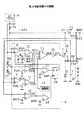
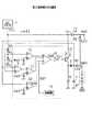
図8は、DC−DCコンバータの従来例を示す。DC−DCコンバータ1は、1チップの半導体集積回路装置上に搭載された制御回路2と、複数の外付け素子とから構成される。
【0004】
制御回路2の出力信号SG1は、PチャネルMOSトランジスタで構成されるスイッチングトランジスタ3のゲートに供給される。スイッチングトランジスタのソースには、電子機器に外付けされるACアダプタ4から、直流電源Vinが抵抗R1を介して供給される。
【0005】
また、直流電源Vinは抵抗R1及びダイオードD1を介して第一の出力端子EX1に供給され、その出力端子EX1から出力される出力電圧Vout1が、電子機器の内部回路に電源電圧として出力される。
【0006】
スイッチングトランジスタ3のドレインは、出力コイル5及び抵抗R2を介して第二の出力端子EX2に接続される。第二の出力端子EX2は、バッテリーBTに接続されるとともに、ダイオードD2を介して出力端子EX1に接続される。そして、第二の出力端子EX2から出力される出力電圧Vout2は、バッテリーBTの充電電圧となる。
【0007】
また、スイッチングトランジスタ3のドレインは、フライホイールダイオード6のカソードに接続され、フライホイールダイオード6のアノードはグランドGNDに接続される。
【0008】
出力コイル5と抵抗R2の接続点は、容量7を介してグランドGNDに接続されている。そして、出力コイル5と容量7とで出力電圧Vout2を平滑化する平滑回路が構成される。
【0009】
制御回路2は、第一及び第二の電流検出回路8,9と、第一〜第三の差電圧増幅回路10,11,12と、PWM比較回路13と、発振回路14と、出力回路15とから構成される。
【0010】
第一の電流検出回路8の入力端子には、抵抗R1の両端子間電圧が入力され、第一の電流検出回路8は抵抗R1の両端子間電圧を増幅した出力信号SG2を第一の差電圧増幅回路10の反転入力端子に出力する。
【0011】
第一の差電圧増幅回路10は、第一の電流検出回路8の出力信号SG2と、非反転入力端子に入力される基準電圧Vref1との差電圧を増幅した出力信号SG3をPWM比較回路13に出力する。
【0012】
第二の電流検出回路9の入力端子には、抵抗R2の両端子間電圧が入力され、第二の電流検出回路9は抵抗R2の両端子間電圧を増幅した出力信号SG4を第二の差電圧増幅回路11の反転入力端子に出力する。
【0013】
第二の差電圧増幅回路11は、第二の電流検出回路9の出力信号SG4と、非反転入力端子に入力される基準電圧Vref2との差電圧を増幅した出力信号SG5をPWM比較回路13に出力する。
【0014】
第三の差電圧増幅回路12の反転入力端子には、充電電圧Vout2が入力される。そして、第三の差電圧増幅回路12は、充電電圧Vout2と、非反転入力端子に入力される基準電圧Vref3との差電圧を増幅した出力信号SG6をPWM比較回路13に出力する。
【0015】
第一〜第三の差電圧増幅回路10,11,12の出力信号SG3,SG5,SG6は、PWM比較回路13の非反転入力端子に入力される。PWM比較回路13の反転入力端子には、発振回路14から出力される所定周波数の三角波信号SG7が入力される。
【0016】
PWM比較回路13は第一〜第三の差電圧増幅回路10,11,12の出力信号SG3,SG5,SG6のうちで最も電圧が低い信号と、三角波信号SG7とを比較する。
【0017】
そして、PWM比較回路13は三角波信号SG7の各周期において、三角波信号SG7の電圧レベルの方が高くなる期間では、Lレベルの出力信号SG8を出力し、三角波信号SG7の電圧レベルの方が低くなる期間では、Hレベルの出力信号SG8を出力する。
【0018】
PWM比較回路13の出力信号SG8は、出力回路15に入力される。出力回路15は、PWM比較回路13の出力信号SG8を反転させた出力信号SG1をデューテイ制御信号としてスイッチングトランジスタ3のゲートに出力する。
【0019】
従って、スイッチングトランジスタ3はデューティ制御信号SG1がHレベルのときオフされ、Lレベルのときオンされる。
このように構成されたDC−DCコンバータでは、ACアダプタ4から直流電圧Vinが供給されると、第一の出力端子EX1から内部回路に電源電圧Vout1及び供給電流I1を出力する。
【0020】
また、制御回路2から出力されるデューティ制御信号SG1に基づいて、スイッチングトランジスタ3がオン動作とオフ動作とを交互に繰り返す。すると、第二の出力端子EX2から充電電流I2がバッテリーBTに供給される。
【0021】
このような動作時において、内部回路への供給電流I1と、バッテリーBTの充電電流I2の和であるACアダプタ4の出力電流Ioが増大すると、抵抗R1の両端子間の電位差が増大し、第一の電流検出回路8の出力信号SG2の電圧レベルが上昇する。
【0022】
すると、第一の差電圧増幅回路10の出力信号SG3の電圧レベルが低下し、この状態で出力信号SG3が出力信号SG5,SG6より低レベルであると、PWM比較回路13の出力信号SG8において、Lレベルの期間が長くなる。
【0023】
この結果、デューティ制御信号SG1に基づいて、スイッチングトランジスタ3のオン時間が短くなり、バッテリーBTの充電電流I2が減少する。
また、ACアダプタ4の出力電流Ioが減少すると、抵抗R1の両端子間の電位差が減少し、第一の電流検出回路8の出力信号SG2の電圧レベルが低下する。
【0024】
すると、第一の差電圧増幅回路10の出力信号SG3の電圧レベルが上昇し、この状態で出力信号SG3が出力信号SG5,SG6より低レベルであると、PWM比較回路13の出力信号SG8において、Lレベルの期間が短くなる。
【0025】
この結果、デューティ制御信号SG1に基づいて、スイッチングトランジスタ3のオン時間が長くなり、バッテリーBTの充電電流I2が増大する。
また、第一の差電圧増幅回路10の出力信号SG3の電圧レベルが、他の差電圧増幅回路11,12の出力信号SG5,SG6より高い場合には、スイッチングトランジスタ3のオン時間は出力信号SG5,SG6のいずれかに基づいて制御される。
【0026】
このような動作により、第一の電流検出回路8の出力信号SG2が基準電圧Vref1に収束するように、すなわち、ACアダプタ4の出力電流Ioが、当該ACアダプタ4の電流供給能力の範囲内となるように制御される。
【0027】
バッテリーBTの充電電流I2が増大して、抵抗R2の両端子間の電位差が増大すると、第二の電流検出回路9の出力信号SG4の電圧レベルが上昇する。
すると、第二の差電圧増幅回路11の出力信号SG5の電圧レベルが低下し、この状態で出力信号SG5が出力信号SG3,SG6より低レベルであると、PWM比較回路13の出力信号SG8において、Lレベルの期間が長くなる。
【0028】
この結果、デューティ制御信号SG1に基づいて、スイッチングトランジスタ3のオン時間が短くなり、バッテリーBTの充電電流I2が減少する。
また、バッテリーBTの充電電流I2が減少すると、抵抗R2の両端子間の電位差が減少し、第二の電流検出回路9の出力信号SG4の電圧レベルが低下する。
【0029】
すると、第二の差電圧増幅回路11の出力信号SG5の電圧レベルが上昇し、この状態で出力信号SG5が出力信号SG3,SG6より低レベルであると、PWM比較回路13の出力信号SG8において、Lレベルの期間が短くなる。
【0030】
この結果、デューティ制御信号SG1に基づいて、スイッチングトランジスタ3のオン時間が長くなり、バッテリーBTの充電電流I2が増大する。
また、第二の差電圧増幅回路11の出力信号SG5の電圧レベルが、他の差電圧増幅回路10,12の出力信号SG3,SG6より高い場合には、スイッチングトランジスタ3のオン時間は出力信号SG3,SG6のいずれかに基づいて制御される。
【0031】
このような動作により、第二の電流検出回路9の出力信号SG4が基準電圧Vref2に収束するように、すなわち、バッテリーBTの充電電流I2が、バッテリーBTに対し過電流とならないような一定値に制御される。
【0032】
バッテリーBTの充電電圧Vout2が上昇すると、第三の差電圧増幅回路12の出力信号SG6の電圧レベルが低下し、この状態で出力信号SG6が出力信号SG3,SG5より低レベルであると、PWM比較回路13の出力信号SG8において、Lレベルの期間が長くなる。
【0033】
この結果、デューティ制御信号SG1に基づいて、スイッチングトランジスタ3のオン時間が短くなり、バッテリーBTの充電電流I2が減少する。
また、バッテリーBTの充電電圧Vout2が低下すると、第三の差電圧増幅回路12の出力信号SG6の電圧レベルが上昇し、この状態で出力信号SG6が出力信号SG3,SG5より低レベルであると、PWM比較回路13の出力信号SG8において、Lレベルの期間が短くなる。
【0034】
この結果、デューティ制御信号SG1に基づいて、スイッチングトランジスタ3のオン時間が長くなり、バッテリーBTの充電電流I2が増大する。
また、第三の差電圧増幅回路12の出力信号SG6の電圧レベルが、他の差電圧増幅回路10,11の出力信号SG3,SG5より高い場合には、スイッチングトランジスタ3のオン時間は出力信号SG3,SG5のいずれかに基づいて制御される。
【0035】
このような動作により、バッテリーBTの充電電圧Vout2が基準電圧Vref3に収束するように、すなわち、バッテリーBTが過充電とならないような一定値に制御される。
【0036】
従って、このDC−DCコンバータでは、第一の電流検出回路8及び第一の差電圧増幅回路10の動作により、ACアダプタ4の出力電流IoがACアダプタ4の電流供給能力の範囲内となるように制御される。
【0037】
また、第二の電流検出回路9及び第二の差電圧増幅回路11の動作により、バッテリーBTの充電電流I2が一定値となるように制御され、第三の差電圧増幅回路12の動作により、充電電圧Vout2が一定値となるように制御される。
【0038】
図9は、第二の従来例を示す。この従来例は、前記第一の従来例から抵抗R1及び第一の電流検出回路8が省略されている。そして、ACアダプタ4の出力端子が抵抗R3,R4を介してグランドGNDに接続されるとともに、抵抗R3,R4の接続点であるノードN1の電圧レベルが第一の差電圧増幅回路10の非反転入力端子に入力されている。その他の構成は前記第一の従来例と同様である。
【0039】
このように構成されたDC−DCコンバータでは、ACアダプタ4の出力電流Ioが増大して、ACアダプタ4の電流供給能力を超えると、ACアダプタ4から出力される直流電圧Vinが低下する。
【0040】
すると、ノードN1の電位が低下して、第一の差電圧増幅回路10の出力信号SG3の電圧レベルが低下し、この状態で出力信号SG3が出力信号SG5,SG6より低レベルであると、PWM比較回路13の出力信号SG8において、Lレベルの期間が長くなる。
【0041】
この結果、デューティ制御信号SG1に基づいて、スイッチングトランジスタ3のオン時間が短くなり、バッテリーBTの充電電流I2が減少するため、ACアダプタ4の出力電流Ioが減少する。
【0042】
このような動作により、ACアダプタ4の出力電流IoはACアダプタ4の電流供給能力の範囲内となるように制御される。また、第二の差電圧増幅回路11の動作により、バッテリーBTの充電電流I2の制御が行われ、第三の差電圧増幅回路12の動作により、バッテリーBTの充電電圧Vout2の制御が行われることは前記第一の従来例と同様である。
【0043】
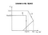
図10において、AはACアダプタの出力電圧−出力電圧特性を示し、BはDC−DCコンバータの充電電圧−充電電流特性を示す。すなわち、ACアダプタ4は直流電圧Vinを一定に維持しながら出力電流Ioを可変とすることができる。
【0044】
また、ACアダプタ4には過電流リミッタが内蔵され、出力電流Ioが動作上限値P1に達すると、過電流リミッタが作動して直流電圧Vinが低下する。そして、出力電流Ioが最大限界値P2に達すると、ACアダプタ4はシャットダウン状態となり、電圧出力及び電流出力を停止する。
【0045】
DC−DCコンバータ1は、一定の充電電圧Vout2を維持しながら充電電流I2でバッテリーBTを充電するが、その充電電流I2の上限値P3はACアダプタ4の出力電流Ioの動作上限値P1より小さい値に設定される。
【0046】
図11は、ACアダプタ4の出力電流Ioが内部回路へ供給電流I1として供給されるとともに、充電電流I2として供給されるとき、供給電流I1と充電電流I2との関係を示すものである。
【0047】
すなわち、内部回路への出力電流I1と充電電流I2との和がACアダプタ4の出力電流Ioとなるため、同図に示すように、出力電流I1と充電電流I2との一方が大きくなれば他方が小さくなる。この関係を示す特性線L1,L2はACアダプタ4の電流供給能力の違いにより、傾きの異なる直線となる。
【0048】
【発明が解決しようとする課題】
上記第一の従来例では、ACアダプタ4の出力電流Ioは、ACアダプタの動作上限値P1より小さくなるように設定される。ACアダプタ4の出力電流Ioが、ACアダプタ4の電流供給能力を超えてしまうと、ACアダプタ4がシャットダウンしてしまうからである。
【0049】
従って、携帯時には小容量のACアダプタを使用し、在宅時には大容量のACアダプタを使用するというように、電流供給能力の異なる複数のACアダプタを取り替えて使用する場合には、電流供給能力の小さいACアダプタを使用してもシャットダウンが発生しないように、出力電流Ioを設定する必要がある。
【0050】
すると、電流供給能力の大きなACアダプタを使用しても、その電流供給能力を有効に使用することはできないという問題点がある。
第二の従来例では、ACアダプタ4の出力電流IoがACアダプタ4の電流供給能力を超えた場合に、ACアダプタ4から出力される直流電圧Vinが低下するため、その直流電圧Vinの低下を第一の差電圧増幅回路10で検出して、充電電流I2を抑制する構成である。
【0051】
従って、電流供給能力の異なる複数のACアダプタを取り替えて使用する場合にも、ACアダプタの電流供給能力を最大限利用することができる。
しかし、電流供給能力の大きいACアダプタでは、電流供給能力を超えた出力電流を出力する場合の出力電圧垂下特性の精度を確保することは容易ではない。従って、ACアダプタの許容出力電力を超えた電力でバッテリーBTを充電することがあり、このような場合にはACアダプタが発熱するという問題点がある。
【0052】
この発明の目的は、異なる電流供給能力を備えたACアダプタを安定して動作させながら、その電流供給能力を最大限に活用し得るDC−DCコンバータを提供することにある。
【0053】
【課題を解決するための手段】
図1は請求項1及び2の原理説明図である。すなわち、DC−DCコンバータは、直流電源Vinの入力に基づいて、内部回路に内部電源Vout1を供給する電源供給回路22と、前記直流電源Vinの入力に基づいて、バッテリーBTに充電電流I2を供給する充電回路23と、前記充電電流I2を制御する制御回路2とを備える。前記制御回路2は、充電電圧制御部24と、充電電流制御部25と、差動充電制御部26と、動的充電制御部27とを備える。請求項1に記載の発明では、充電電圧制御部24は、前記バッテリーBTの充電電圧Vout2をしきい値と比較し、その比較結果に基づいて該バッテリーBTの充電電流I2を制御する。充電電流制御部25は、前記充電回路23からバッテリーBTに供給される充電電流I2をしきい値と比較し、その比較結果に基づいて該充電電流I2を制御する。差動充電制御部26は、前記直流電源Vinからの入力電流Ioを第1のしきい値と比較し、その比較結果に基づいて前記充電電流I2を制御し、前記直流電源からの入力電圧Vinが第2のしきい値よりも小さいことを示す信号に応答して前記第1のしきい値を小さく設定するしきい値変更回路を有する。このしきい値変更回路は、前記充電電圧がしきい値を超えたとき、前記充電電圧制御部の比較結果に基づいて、前記第1のしきい値として入力される基準電圧を変更後の基準電圧から変更前の基準電圧にリセットするリセット回路を備える。動的充電制御部27は、前記直流電源からの入力電圧Vinをしきい値と比較し、その比較結果に基づいて前記充電電流I2を制御する。
また、請求項2に記載の発明では、充電電圧制御部24は、前記バッテリーBTの充電電圧Vout2をしきい値と比較し、その比較結果に基づいて該バッテリーBTの充電電流I2を制御する。充電電流制御部25は、前記充電回路23からバッテリーBTに供給される充電電流I2を第3のしきい値と比較し、その比較結果に基づいて該充電電流I2を制御し、前記直流電源からの入力電圧が第4のしきい値よりも小さいことを示す信号に応答して前記第3のしきい値を小さく設定するしきい値変更回路を有する。しきい値変更回路は、前記充電電圧がしきい値を超えたとき、前記充電電圧制御部の比較結果に基づいて、前記第3のしきい値として入力される基準電圧を変更後の基準電圧から変更前の基準電圧にリセットするリセット回路を備える。差動充電制御部26は、前記直流電源Vinからの入力電流Ioをしきい値と比較し、その比較結果に基づいて前記充電電流I2を制御する。動的充電制御部27は、前記直流電源からの入力電圧Vinをしきい値と比較し、その比較結果に基づいて前記充電電流I2を制御する。
【0054】
【発明の実施の形態】
(第一の実施の形態)
図2は、この発明を具体化したDC−DCコンバータの第一の実施の形態を示す。
【0055】
この実施の形態は、前記第一の従来例の制御回路2の構成を一部変更したものであり、他の同一構成部分は同一符号を付して詳細な説明を省略する。
制御回路2において、第一の電流検出回路8及び第一の差電圧増幅回路10は、前記第一の従来例と同様であり、第一の電流検出回路8の入力端子には、抵抗R1の両端子間の電位差が入力される。
【0056】
第二の電流検出回路9及び第二の差電圧増幅回路11は、前記第一の従来例と同様であり、第二の電流検出回路9の入力端子には、抵抗R2の両端子間の電位差が入力される。
【0057】
そして、第二の電流検出回路9及び第二の差電圧増幅回路11は、抵抗R2の両端子間電圧に基づいて充電電流I2を制御する充電電流制御部として動作する。
【0058】
第三の差電圧増幅回路12の反転入力端子には、前記第一の従来例と同様に、充電電圧Vout2が入力される。
第三の差電圧増幅回路12は、充電電流I2を制御することにより充電電圧Vout2を制御する充電電圧制御部として動作する。
【0059】
ACアダプタ4の出力端子は、前記第二の従来例と同様に、抵抗R3,R4を介してグランドGNDに接続され、その抵抗R3,R4の接続点であるノードN1は、第四の差電圧増幅回路16の非反転入力端子に接続される。
【0060】
前記第四の差電圧増幅回路16の反転入力端子には、基準電圧Vref4が入力される。
前記抵抗R1の抵抗値は、大容量のACアダプタ4を使用したとき、その出力電流Ioが動作上限値P1付近に達すると、第一の電流検出回路8及び第一の差電圧増幅回路10の動作に基づいて、充電電流I2が抑制されるように設定する。
【0061】
次に、このように構成されたDC−DCコンバータの動作を説明する。充電電流I2は第二の電流検出回路9及び第二の差電圧増幅回路11の動作により、前記従来例と同様に制御される。
【0062】
また、充電電圧Vout2は第三の差電圧増幅回路12の動作により、前記従来例と同様に制御される。
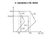
図5において、A1は大容量のACアダプタの出力電圧−出力電流特性を示し、A2は小容量のACアダプタの出力電圧−出力電流特性を示す。また、B1はこの実施の形態で大容量のACアダプタ使用した場合の充電電圧−充電電流特性を示し、B2は小容量のACアダプタを使用した場合の充電電圧−充電電流特性を示す。
【0063】
大容量のACアダプタ4を使用した状態で、出力電流Ioが動作上限値P1付近に達すると、抵抗R1の両端子間の電位差が増大し、その電位差に基づいて第一の電流検出回路8の出力信号SG2の電圧レベルが上昇する。
【0064】
すると、第一の差電圧増幅回路10の出力信号SG3の電圧レベルが低下し、デューティ制御信号SG1のLレベルの期間が短くなる。この結果、スイッチングトランジスタ3のオン時間が短くなって、充電電流I2が減少する。従って、出力電流Ioは大容量のACアダプタ4の動作上限値P4を超えない範囲で制御される。
【0065】
このような動作により、抵抗R1、第一の電流検出回路8及び第二の差電圧増幅回路10は、大容量のACアダプタ4を使用したとき、動作上限値P4付近の出力電流Ioを検出して、充電電流I2を減少させる差動充電制御部として動作する。
【0066】
小容量のACアダプタ4を使用したとき、抵抗R1に流れる出力電流はIoは小さいので、その出力電流Ioに基づいて差動充電制御部により充電電流I2が抑制されることはない。
【0067】
そして、小容量のACアダプタ4から当該アダプタの動作上限値P5を超える出力電流Ioが出力されると、ACアダプタ4の出力電圧Vinが低下する。
すると、第四の差電圧増幅回路16の出力電圧が低下し、デューティ制御信号SG1のLレベルの期間が短くなる。この結果、スイッチングトランジスタ3のオン時間が短くなって、充電電流I2が減少する。
【0068】
小容量のACアダプタ4は、電流供給能力を超えた出力電流を出力する場合の出力電圧垂下特性の精度を確保することは容易である。従って、動作上限値P5を超える出力電流Ioが出力されるときには、充電電流I2を減少させて、出力電流Ioを確実に減少させることができる。
【0069】
このような動作により、抵抗R3,R4、第四の差電圧増幅回路16は、ACアダプタ4の電流供給能力を超えた動作を動的に検出して、充電電流I2を制御する動的充電制御部として動作する。
【0070】
上記のように構成されたDC−DCコンバータでは、次に示す作用効果を得ることができる。
(1)抵抗R2の両端子間電圧に基づく第二の電流検出回路9及び第二の差電圧増幅回路11の動作により、充電電流I2を一定に維持することができる。
【0071】
(2)充電電圧Vout2に基づく第三の差電圧増幅回路12の動作により、充電電圧Vout2を一定に維持することができる。
(3)大容量のACアダプタを使用したとき、差動充電制御部の動作により、出力電流Ioを動作上限値P4以下に確実に維持することができる。従って、大容量のACアダプタの電流供給能力を十分に活用しながら、許容出力電力を超えた電力出力を防止して、ACアダプタの発熱を未然に防止することができる。
【0072】
(4)小容量のACアダプタを使用したとき、動的充電制御部の動作により、ACアダプタの電流供給能力を最大限活用した出力電流Ioを出力することができる。
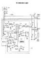
(第二の実施の形態)
図3は、第二の実施の形態を示す。この実施の形態は、前記第一の実施の形態に第一及び第二の比較回路17,18及びラッチ回路19を加えたものである。
【0073】
すなわち、第四の差電圧増幅回路16の出力信号SG9は、PWM比較回路13に出力されるとともに、第一の比較回路17の反転入力端子に入力される。
前記第一の比較回路17の非反転入力端子には、基準電圧Vref5が入力される。そして、第一の比較回路17は第四の差電圧増幅回路16の出力信号SG9の電圧レベルが基準電圧Vref5より低くなった時、Hレベルの出力信号をラッチ回路19のセット端子Sに出力する。
【0074】
第三の差電圧増幅回路12の出力信号SG6は、PWM比較回路13に出力されるとともに、前記第二の比較回路18の反転入力端子に入力される。
前記第二の比較回路18の非反転入力端子には、基準電圧Vref6が入力される。そして、第二の比較回路18は第三の差電圧増幅回路12の出力信号SG6の電圧レベルが基準電圧Vref6より低くなると、Hレベルの出力信号を前記ラッチ回路20のリセット端子Rに出力する。
【0075】
前記ラッチ回路は、セット端子SにHレベルの信号が入力されると、Hレベルの出力信号Qを出力し、リセット端子RにHレベルの信号が入力されると、Lレベルの出力信号Qを出力する。
【0076】
前記ラッチ回路19の出力信号Qはスイッチ回路20に入力される。前記スイッチ回路20は、前記ラッチ回路19からLレベルの信号が入力されると、基準電圧Vref1を第一の差電圧増幅回路10の非反転入力端子に入力し、前記ラッチ回路19からHレベルの信号が入力されると、基準電圧Vref7を第一の差電圧増幅回路10の非反転入力端子に入力する。
【0077】
前記基準電圧Vref1は、前記第一の実施の形態と同一電圧である。前記基準電圧Vref7は基準電圧Vref1より低電圧であって、第一の電流検出回路8及び第一の差電圧増幅回路10を、小容量ACアダプタ4から出力される出力電流Ioに基づいて、差動充電制御部として動作させるための基準電圧である。
【0078】
上記のように構成されたDC−DCコンバータでは、ラッチ回路19の出力信号Qの初期値はLレベルに設定されるので、第一の差電圧増幅回路10には、スイッチ回路20を介して基準電圧Vref1が供給されている。
【0079】
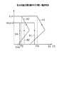
この状態で大容量のACアダプタ4を使用する場合には、第一の電流検出回路8及び第一の差電圧増幅回路10は、前記第一の実施の形態と同様な差動充電制御部として動作し、図6に示すように、出力電流Ioは動作上限値P4を超えない範囲で制御される。
【0080】
そして、充電電圧Vout2が上昇して第三の差電圧増幅回路12の出力信号SG6の電圧レベルが低下し、基準電圧Vref6より低くなると、第二の比較回路18の出力信号がHレベルとなり、ラッチ回路19の出力信号QはLレベルに維持される。
【0081】
従って、大容量のACアダプタ4を使用する場合には、前記第一の実施の形態と同様に動作する。
小容量のACアダプタを使用する場合、第一の差電圧増幅回路10に基準電圧Vref1が入力されている状態では、第一の差電圧増幅回路10が小容量のACアダプタの出力電流Ioに基づいて、差動充電制御部として動作することはなく、第一の実施の形態と同様に、図6にB2で示す充電電圧−充電電流特性で動作する。
【0082】
この状態で、図6に示すように、出力電流Ioが当該アダプタの動作上限値P5を超えると、ACアダプタ4の出力電圧Vinが低下して、ノードN1の電位が低下する。
【0083】
すると、第四の差電圧増幅回路16の出力信号SG9の電圧レベルが低下し、基準電圧Vref5より低くなって、第一の比較回路17からHレベルの出力信号が出力される。
【0084】
第一の比較回路17からのHレベルの出力信号に基づいて、ラッチ回路19からHレベルの出力信号Qが出力され、その出力信号Qに基づいてスイッチ回路20が切替えられ、第一の差電圧増幅回路10には基準電圧Vref7が供給される。
【0085】
すると、第一の差電圧増幅回路10の出力信号SG3の電圧レベルが低下し、PWM比較回路13はその出力信号SG3に基づいて動作する状態となる。そして、その出力信号SG3に基づいてスイッチングトランジスタ3のオン時間が短縮され、図6にB3で示す充電電圧−充電電流特性で動作する状態となる。
【0086】
この結果、充電電流I2が減少して、充電電流I2の上限値は、差動充電制御による電流値Ib3に減少する。
従って、小さな充電電流によりバッテリーBTの充電が継続され、やがて充電電圧Vout2が所定電圧まで上昇すると、第三の差電圧増幅回路12の出力電圧SG6の電圧レベルが基準電圧Vref6より低くなる。
【0087】
すると、第二の比較回路18からHレベルの信号が出力され、ラッチ回路19の出力信号QがLレベルとなって、スイッチ回路20が切替えられ、第一の差電圧増幅回路10に基準電圧Vref1が供給される状態に復帰する。
【0088】
上記のように構成されたDC−DCコンバータでは、前記第一の実施の形態と同様な作用効果に加えて、次に示す作用効果を得ることができる。
(1)小容量のACアダプタ4を使用する場合、動的充電制御部でACアダプタ4の出力電圧Vinの低下を検出した後は、基準電圧Vref1を自動的に基準電圧Vref7に切替えて、差動充電制御部で出力電流Ioを制御することができる。従って、出力電圧Vinの低下を検出した後は、小さな充電電流I2でバッテリーBTを充電し続けることにより、ACアダプタ4を安定して動作させることができる。
(第三の実施の形態)
図4は、第三の実施の形態を示す。この実施の形態は、前記第二の実施の形態の第一の差電圧増幅回路10に供給する基準電圧を、第一の実施の形態と同様な基準電圧Vref1のみとし、第二の差電圧増幅回路11には、スイッチ回路21を介して、基準電圧Vref2,Vref8のいずれかを供給可能としている。
【0089】
前記スイッチ回路21は、前記第二の実施の形態と同様なラッチ回路19の出力信号Qに基づいて切替え動作を行う。そして、ラッチ回路19の出力信号QがHレベルとなると、基準電圧Vref8を第二の差電圧増幅回路11の非反転入力端子に入力し、ラッチ回路19の出力信号QがLレベルとなると、基準電圧Vref2を第二の差電圧増幅回路11の非反転入力端子に入力する。
【0090】
前記基準電圧Vref2は、前記第一及び第二の実施の形態と同一電圧である。前記基準電圧Vref8は、基準電圧Vref2より低電圧に設定され、バッテリーBTの充電電流I2を減少させるための基準電圧である。そして、上記以外の構成は、前記第二の実施の形態と同様である。
【0091】
上記のように構成されたDC−DCコンバータでは、ラッチ回路19の出力信号Qの初期値はLレベルに設定されるので、第二の差電圧増幅回路11には、スイッチ回路21を介して基準電圧Vref2が供給されている。
【0092】
この状態で大容量のACアダプタ4を使用する場合には、第一の電流検出回路8及び第一の差電圧増幅回路10は、前記第一の実施の形態と同様な差動充電制御部として動作し、図7に示すように、出力電流Ioは動作上限値P4を超えない範囲で制御される。
【0093】
そして、充電電圧Vout2が上昇して第三の差電圧増幅回路12の出力信号SG6の電圧レベルが低下し、基準電圧Vref6より低くなると、第二の比較回路18の出力信号がHレベルとなり、ラッチ回路19の出力信号QはLレベルに維持される。
【0094】
従って、大容量のACアダプタ4を使用する場合には、前記第一の実施の形態と同様に動作する。
小容量のACアダプタを使用する場合、第二の差電圧増幅回路10に基準電圧Vref8が入力されている状態では、第一の実施の形態と同様に、図7にB2で示す充電電圧−充電電流特性で動作する。
【0095】
この状態で、図7に示すように、出力電流Ioが当該アダプタの動作上限値P5を超えると、ACアダプタ4の出力電圧Vinが低下して、ノードN1の電位が低下する。
【0096】
すると、第四の差電圧増幅回路16の出力信号SG9の電圧レベルが低下し、基準電圧Vref5より低くなって、第一の比較回路17からHレベルの出力信号が出力される。
【0097】
第一の比較回路17からのHレベルの出力信号に基づいて、ラッチ回路19からHレベルの出力信号Qが出力され、その出力信号Qに基づいてスイッチ回路21が切替えられ、第二の差電圧増幅回路11には基準電圧Vref8が供給される。
【0098】
すると、第二の差電圧増幅回路11の出力信号SG5の電圧レベルが低下し、PWM比較回路13はその出力信号SG5に基づいて動作する状態となる。そして、その出力信号SG5に基づいてスイッチングトランジスタ3のオン時間が短縮され、充電電流I2が減少して、出力電流Ioの上限値は、差動充電制御による電流値Ib4に減少する。
【0099】
すなわち、第二の差電圧増幅回路11に基準電圧Vref8が供給されることにより、図7にB4で示す充電電圧−充電電流特性で動作する状態となる。
従って、小さな充電電流によりバッテリーBTの充電が継続され、やがて充電電圧Vout2が所定電圧まで上昇すると、第三の差電圧増幅回路12の出力電圧SG6の電圧レベルが基準電圧Vref6より低くなる。
【0100】
すると、第二の比較回路18からHレベルの信号が出力され、ラッチ回路19の出力信号QがLレベルとなって、スイッチ回路21が切替えられ、第二の差電圧増幅回路11に基準電圧Vref2が供給される状態に復帰する。
【0101】
上記のように構成されたDC−DCコンバータでは、前記第一の実施の形態で得られた作用効果に加えて、次に示す作用効果を得ることができる。
(1)小容量のACアダプタ4を使用する場合、動的充電制御部でACアダプタ4の出力電圧Vinの低下を検出した後は、基準電圧Vref2を自動的に基準電圧Vref8に切替えて、充電電流制御部で充電電流I2を制御することができる。従って、出力電圧Vinの低下を検出した後は、小さな充電電流I2でバッテリーBTを充電し続けることにより、ACアダプタ4を安定して動作させることができる。
【0102】
(2)出力電圧Vinの低下を検出した後の充電電流Ioの最大値は、基準電圧Vref8により適宜に設定することができる。
(付記1) 直流電源の入力に基づいて、内部回路に内部電源を供給する電源供給回路と、
前記直流電源の入力に基づいて、バッテリーに充電電流を供給する充電回路と、
前記充電電流を制御する制御回路と
を備えたDC−DCコンバータであって、
前記制御回路は、
前記バッテリーの充電電圧をしきい値と比較し、その比較結果に基づいて該バッテリーの充電電流を制御する充電電圧制御部と、
前記充電回路からバッテリーに供給される充電電流をしきい値と比較し、その比較結果に基づいて該充電電流を制御する充電電流制御部と、
前記直流電源の出力電流をしきい値と比較し、その比較結果に基づいて前記充電電流を制御する差動充電制御部と、
前記直流電源の出力電圧をしきい値と比較し、その比較結果に基づいて前記充電電流を制御する動的充電制御部と
を備えたことを特徴とするDC−DCコンバータ。(1)
(付記2) 前記差動充電制御部は、
異なる大きさの入力電流のうち、所定のしきい値以上の入力電流を検出した検出信号を出力する入力電流検出部と、
前記入力電流検出部の検出信号に基づいて、前記充電電流を減少させる制御信号を前記充電回路に出力する出力部と
から構成し、
前記動的充電制御部は、
前記入力電圧を所定のしきい値と比較することにより、該入力電圧の低下を検出した検出信号を出力する入力電圧検出部と、
前記入力電圧検出部の検出信号に基づいて、前記充電電流を減少させる制御信号を前記充電回路に出力する出力部と
から構成したことを特徴とする付記1記載のDC−DCコンバータ。(2)
(付記3) 前記入力電流検出部は、前記入力電圧検出部の検出信号に基づいて、前記しきい値を小さくするしきい値変更回路を備えたことを特徴とする付記2記載のDC−DCコンバータ。(3)
(付記4) 前記充電電流制御部は、前記入力電圧検出部の検出信号に基づいて、前記充電電流を検出するしきい値を小さくするしきい値変更回路を備えたことを特徴とする付記2記載のDC−DCコンバータ。(4)
(付記5) 前記しきい値変更回路は、しきい値として入力される基準電圧を前記入力電圧検出部の検出信号に基づいて変更する回路で構成したことを特徴とする付記3または4記載のDC−DCコンバータ。(5)
(付記6)付記1乃至5のいずれかに記載の前記制御回路を1チップ上に搭載したことを特徴とするDC−DCコンバータ用半導体集積回路装置。(6)
(付記7) 前記しきい値変更回路は、前記充電電圧がしきい値を超えたとき、前記充電電圧制御部の比較結果に基づいて、前記変更後の基準電圧を変更前の基準電圧にリセットするリセット回路を備えたことを特徴とする付記5記載のDC−DCコンバータ。
(付記8) 前記リセット回路は、前記動的充電制御部の入力電圧検出部から出力される検出信号と、前記充電電圧制御部の比較結果とに基づいて、前記基準電圧を交互に変更するための出力信号を出力するラッチ回路で構成したことを特徴とする付記7記載のDC−DCコンバータ。
【0103】
【発明の効果】
以上詳述したように、この発明は異なる電流供給能力を備えたACアダプタを安定して動作させながら、その電流供給能力を最大限に活用し得るDC−DCコンバータを提供することができる。
【図面の簡単な説明】
【図1】 本発明の原理説明図である。
【図2】 第一の実施の形態を示す回路図である。
【図3】 第二の実施の形態を示す回路図である。
【図4】 第三の実施の形態を示す回路図である。
【図5】 第一の実施の形態の動作を示す電圧−電流特性図である。
【図6】 第二の実施の形態の動作を示す電圧−電流特性図である。
【図7】 第三の実施の形態の動作を示す電圧−電流特性図である。
【図8】 第一の従来例を示す回路図である。
【図9】 第二の従来例を示す回路図である。
【図10】 従来例の動作を示す電圧−電流特性図である。
【図11】 充電電流と内部回路での消費電流との関係を示す説明図である。
【符号の説明】
2 制御回路
22 電源供給回路
23 充電回路
24 充電電圧制御部
25 充電電流制御部
26 差動充電制御部
Vin 直流電源
Io 出力電流
I2 充電電流
Vout1 内部電源
Vout2 充電電圧
BT バッテリー[0001]
BACKGROUND OF THE INVENTION
The present invention relates to a DC-DC converter used as a power source for portable electronic devices.
[0002]
In recent years, in portable electronic devices such as notebook computers, a DC-DC that charges a battery provided as an auxiliary power source while supplying power to an internal circuit based on a DC power source supplied from an external AC adapter. A converter is installed.
In such a DC-DC converter, in order to operate the AC adapter stably and safely, the sum of the consumption current in the internal circuit and the charging current of the battery is smaller than the current supply capability of the AC adapter. It is set to be. Even when using different AC adapters with different current supply capacities, it is necessary to make the most of the current supply capacities of the AC adapters.
[0003]
[Prior art]
FIG. 8 shows a conventional example of a DC-DC converter. The DC-
[0004]
The output signal SG1 of the
[0005]
The DC power supply Vin is supplied to the first output terminal EX1 via the resistor R1 and the diode D1, and the output voltage Vout1 output from the output terminal EX1 is output as a power supply voltage to the internal circuit of the electronic device.
[0006]
The drain of the
[0007]
The drain of the
[0008]
A connection point between the
[0009]
The
[0010]
The voltage between both terminals of the resistor R1 is input to the input terminal of the first
[0011]
The first differential
[0012]
The voltage between both terminals of the resistor R2 is input to the input terminal of the second
[0013]
The second differential
[0014]
The charging voltage Vout2 is input to the inverting input terminal of the third differential
[0015]
The output signals SG3, SG5, SG6 of the first to third differential
[0016]
The
[0017]
In each period of the triangular wave signal SG7, the
[0018]
The output signal SG8 of the
[0019]
Accordingly, the
In the DC-DC converter configured as described above, when the DC voltage Vin is supplied from the
[0020]
Further, based on the duty control signal SG1 output from the
[0021]
In such an operation, when the output current Io of the
[0022]
Then, the voltage level of the output signal SG3 of the first differential
[0023]
As a result, the ON time of the switching
Further, when the output current Io of the
[0024]
Then, the voltage level of the output signal SG3 of the first differential
[0025]
As a result, based on the duty control signal SG1, the ON time of the switching
On the other hand, when the voltage level of the output signal SG3 of the first differential
[0026]
By such an operation, the output signal SG2 of the first
[0027]
When the charging current I2 of the battery BT increases and the potential difference between both terminals of the resistor R2 increases, the voltage level of the output signal SG4 of the second
Then, the voltage level of the output signal SG5 of the second differential
[0028]
As a result, the ON time of the switching
Further, when the charging current I2 of the battery BT decreases, the potential difference between both terminals of the resistor R2 decreases, and the voltage level of the output signal SG4 of the second
[0029]
Then, the voltage level of the output signal SG5 of the second differential
[0030]
As a result, based on the duty control signal SG1, the ON time of the switching
On the other hand, when the voltage level of the output signal SG5 of the second differential
[0031]
By such an operation, the output signal SG4 of the second
[0032]
When the charging voltage Vout2 of the battery BT increases, the voltage level of the output signal SG6 of the third differential
[0033]
As a result, the ON time of the switching
Further, when the charging voltage Vout2 of the battery BT decreases, the voltage level of the output signal SG6 of the third differential
[0034]
As a result, based on the duty control signal SG1, the ON time of the switching
When the voltage level of the output signal SG6 of the third differential
[0035]
By such an operation, the charging voltage Vout2 of the battery BT is controlled to a constant value so as to converge to the reference voltage Vref3, that is, the battery BT is not overcharged.
[0036]
Therefore, in this DC-DC converter, the operation of the first
[0037]
Further, the operation of the second
[0038]
FIG. 9 shows a second conventional example. In this conventional example, the resistor R1 and the first
[0039]
In the DC-DC converter configured as described above, when the output current Io of the
[0040]
Then, the potential of the node N1 decreases, the voltage level of the output signal SG3 of the first differential
[0041]
As a result, the on-time of the switching
[0042]
With such an operation, the output current Io of the
[0043]
In FIG. 10, A shows the output voltage-output voltage characteristic of the AC adapter, and B shows the charge voltage-charge current characteristic of the DC-DC converter. That is, the
[0044]
The
[0045]
The DC-
[0046]
FIG. 11 shows the relationship between the supply current I1 and the charging current I2 when the output current Io of the
[0047]
That is, since the sum of the output current I1 and the charging current I2 to the internal circuit becomes the output current Io of the
[0048]
[Problems to be solved by the invention]
In the first conventional example, the output current Io of the
[0049]
Therefore, when a plurality of AC adapters having different current supply capacities are used, such as using a small-capacity AC adapter when carrying and using a large-capacity AC adapter at home, the current supply capability is small. It is necessary to set the output current Io so that shutdown does not occur even when the AC adapter is used.
[0050]
Then, even if an AC adapter having a large current supply capability is used, the current supply capability cannot be effectively used.
In the second conventional example, when the output current Io of the
[0051]
Therefore, even when a plurality of AC adapters having different current supply capacities are replaced and used, the current supply capability of the AC adapter can be utilized to the maximum extent.
However, with an AC adapter having a large current supply capability, it is not easy to ensure the accuracy of the output voltage drooping characteristic when outputting an output current exceeding the current supply capability. Therefore, the battery BT may be charged with power exceeding the allowable output power of the AC adapter. In such a case, there is a problem that the AC adapter generates heat.
[0052]
An object of the present invention is to provide a DC-DC converter that can make maximum use of its current supply capability while stably operating AC adapters having different current supply capabilities.
[0053]
[Means for Solving the Problems]
FIG. 1 is a diagram for explaining the principle of
In the second aspect of the invention, the charging voltage control unit 24 compares the charging voltage Vout2 of the battery BT with a threshold value, and controls the charging current I2 of the battery BT based on the comparison result. The charging current control unit 25 compares the charging current I2 supplied from the charging
[0054]
DETAILED DESCRIPTION OF THE INVENTION
(First embodiment)
FIG. 2 shows a first embodiment of a DC-DC converter embodying the present invention.
[0055]
In this embodiment, the configuration of the
In the
[0056]
The second
[0057]
The second
[0058]
The charging voltage Vout2 is input to the inverting input terminal of the third differential
The third differential
[0059]
Similarly to the second conventional example, the output terminal of the
[0060]
A reference voltage Vref4 is input to the inverting input terminal of the fourth differential
The resistance value of the resistor R1 is such that when the large-
[0061]
Next, the operation of the DC-DC converter configured as described above will be described. The charging current I2 is controlled by the operations of the second
[0062]
The charging voltage Vout2 is controlled by the operation of the third differential
In FIG. 5, A1 shows the output voltage-output current characteristic of the large capacity AC adapter, and A2 shows the output voltage-output current characteristic of the small capacity AC adapter. B1 shows the charging voltage-charging current characteristic when a large capacity AC adapter is used in this embodiment, and B2 shows the charging voltage-charging current characteristic when a small capacity AC adapter is used.
[0063]
When the output current Io reaches the vicinity of the operation upper limit value P1 in the state where the large
[0064]
Then, the voltage level of the output signal SG3 of the first differential
[0065]
By such an operation, the resistor R1, the first
[0066]
When the small-
[0067]
When an output current Io exceeding the operation upper limit value P5 of the adapter is output from the small
Then, the output voltage of the fourth differential
[0068]
The small-
[0069]
With such an operation, the resistors R3 and R4 and the fourth differential
[0070]
With the DC-DC converter configured as described above, the following operational effects can be obtained.
(1) The charging current I2 can be kept constant by the operations of the second
[0071]
(2) The charging voltage Vout2 can be kept constant by the operation of the third differential
(3) When a large-capacity AC adapter is used, the output current Io can be reliably maintained below the operation upper limit value P4 by the operation of the differential charge control unit. Therefore, while fully utilizing the current supply capability of the large-capacity AC adapter, it is possible to prevent the power output exceeding the allowable output power and prevent the AC adapter from generating heat.
[0072]
(4) When a small-capacity AC adapter is used, an output current Io that makes the best use of the current supply capability of the AC adapter can be output by the operation of the dynamic charge control unit.
(Second embodiment)
FIG. 3 shows a second embodiment. In this embodiment, first and
[0073]
That is, the output signal SG9 of the fourth differential
A reference voltage Vref5 is input to the non-inverting input terminal of the
[0074]
The output signal SG6 of the third differential
A reference voltage Vref6 is input to the non-inverting input terminal of the
[0075]
The latch circuit outputs an H level output signal Q when an H level signal is input to the set terminal S, and outputs an L level output signal Q when an H level signal is input to the reset terminal R. Output.
[0076]
The output signal Q of the
[0077]
The reference voltage Vref1 is the same voltage as in the first embodiment. The reference voltage Vref7 is lower than the reference voltage Vref1, and the first
[0078]
In the DC-DC converter configured as described above, since the initial value of the output signal Q of the
[0079]
When the large
[0080]
When the charging voltage Vout2 increases and the voltage level of the output signal SG6 of the third differential
[0081]
Therefore, when the large
When a small-capacity AC adapter is used, the first differential
[0082]
In this state, as shown in FIG. 6, when the output current Io exceeds the operation upper limit value P5 of the adapter, the output voltage Vin of the
[0083]
Then, the voltage level of the output signal SG9 of the fourth differential
[0084]
Based on the H level output signal from the
[0085]
Then, the voltage level of the output signal SG3 of the first differential
[0086]
As a result, the charging current I2 decreases, and the upper limit value of the charging current I2 decreases to the current value Ib3 by the differential charging control.
Therefore, when the charging of the battery BT is continued by a small charging current and the charging voltage Vout2 eventually rises to a predetermined voltage, the voltage level of the output voltage SG6 of the third differential
[0087]
Then, an H level signal is output from the
[0088]
In the DC-DC converter configured as described above, the following operational effects can be obtained in addition to the operational effects similar to those of the first embodiment.
(1) When using a small-
(Third embodiment)
FIG. 4 shows a third embodiment. In this embodiment, the reference voltage supplied to the first differential
[0089]
The
[0090]
The reference voltage Vref2 is the same voltage as in the first and second embodiments. The reference voltage Vref8 is set to a voltage lower than the reference voltage Vref2, and is a reference voltage for reducing the charging current I2 of the battery BT. The configuration other than the above is the same as that of the second embodiment.
[0091]
In the DC-DC converter configured as described above, since the initial value of the output signal Q of the
[0092]
When the large
[0093]
When the charging voltage Vout2 increases and the voltage level of the output signal SG6 of the third differential
[0094]
Therefore, when the large
When a small-capacity AC adapter is used, in the state where the reference voltage Vref8 is input to the second differential
[0095]
In this state, as shown in FIG. 7, when the output current Io exceeds the operation upper limit value P5 of the adapter, the output voltage Vin of the
[0096]
Then, the voltage level of the output signal SG9 of the fourth differential
[0097]
Based on the H level output signal from the
[0098]
Then, the voltage level of the output signal SG5 of the second differential
[0099]
That is, when the reference voltage Vref8 is supplied to the second differential
Therefore, when the charging of the battery BT is continued by a small charging current and the charging voltage Vout2 eventually rises to a predetermined voltage, the voltage level of the output voltage SG6 of the third differential
[0100]
Then, an H level signal is output from the
[0101]
In the DC-DC converter configured as described above, the following operational effects can be obtained in addition to the operational effects obtained in the first embodiment.
(1) When a small
[0102]
(2) The maximum value of the charging current Io after detecting the decrease in the output voltage Vin can be appropriately set by the reference voltage Vref8.
(Supplementary Note 1) A power supply circuit that supplies internal power to an internal circuit based on input of a DC power supply;
A charging circuit for supplying a charging current to the battery based on the input of the DC power supply;
A control circuit for controlling the charging current;
A DC-DC converter comprising:
The control circuit includes:
A charging voltage controller that compares the charging voltage of the battery with a threshold value and controls the charging current of the battery based on the comparison result;
A charging current controller that compares the charging current supplied to the battery from the charging circuit with a threshold value and controls the charging current based on the comparison result;
A differential charge control unit that compares the output current of the DC power supply with a threshold value and controls the charging current based on the comparison result;
A dynamic charge controller that compares the output voltage of the DC power supply with a threshold value and controls the charging current based on the comparison result;
A DC-DC converter comprising: (1)
(Supplementary Note 2) The differential charge control unit
An input current detection unit that outputs a detection signal that detects an input current that is equal to or greater than a predetermined threshold among input currents of different magnitudes;
An output unit for outputting a control signal for reducing the charging current to the charging circuit based on a detection signal of the input current detecting unit;
Consisting of
The dynamic charge controller is
An input voltage detector that outputs a detection signal that detects a decrease in the input voltage by comparing the input voltage with a predetermined threshold;
An output unit for outputting a control signal for reducing the charging current to the charging circuit based on a detection signal of the input voltage detecting unit;
It is composed of
(Additional remark 3) The said input current detection part was equipped with the threshold value change circuit which makes the said threshold value small based on the detection signal of the said input voltage detection part, It is characterized by the above-mentioned.
(Additional remark 4) The said charging current control part was equipped with the threshold value change circuit which makes the threshold value which detects the said charging current small based on the detection signal of the said input voltage detection part, It is characterized by the above-mentioned.
(Additional remark 5) The said threshold value change circuit was comprised with the circuit which changes the reference voltage input as a threshold value based on the detection signal of the said input voltage detection part, It is characterized by the above-mentioned.Appendix The DC-DC converter according to 3 or 4. (5)
(Appendix 6)Appendix 6. A semiconductor integrated circuit device for a DC-DC converter, wherein the control circuit according to any one of 1 to 5 is mounted on one chip. (6)
(Supplementary Note 7) When the charging voltage exceeds the threshold value, the threshold value changing circuit resets the changed reference voltage to the reference voltage before the changing based on the comparison result of the charging voltage control unit. 6. The DC-DC converter according to
(Supplementary Note 8) The reset circuit alternately changes the reference voltage based on the detection signal output from the input voltage detection unit of the dynamic charge control unit and the comparison result of the charge voltage control unit. The DC-DC converter according to
[0103]
【The invention's effect】
As described in detail above, the present invention can provide a DC-DC converter that can make maximum use of its current supply capability while stably operating AC adapters having different current supply capabilities.
[Brief description of the drawings]
FIG. 1 is a diagram illustrating the principle of the present invention.
FIG. 2 is a circuit diagram showing a first embodiment.
FIG. 3 is a circuit diagram showing a second embodiment.
FIG. 4 is a circuit diagram showing a third embodiment.
FIG. 5 is a voltage-current characteristic diagram showing the operation of the first embodiment.
FIG. 6 is a voltage-current characteristic diagram showing the operation of the second embodiment.
FIG. 7 is a voltage-current characteristic diagram showing the operation of the third embodiment.
FIG. 8 is a circuit diagram showing a first conventional example.
FIG. 9 is a circuit diagram showing a second conventional example.
FIG. 10 is a voltage-current characteristic diagram showing the operation of a conventional example.
FIG. 11 is an explanatory diagram showing a relationship between a charging current and a consumption current in an internal circuit.
[Explanation of symbols]
2 Control circuit
22 Power supply circuit
23 Charging circuit
24 Charge voltage controller
25 Charging current controller
26 Differential charge controller
Vin DC power supply
Io output current
I2 charging current
Vout1 internal power supply
Vout2 charge voltage
BT battery
Claims (6)
Translated fromJapanese前記直流電源の入力に基づいて、バッテリーに充電電流を供給する充電回路と、
前記充電電流を制御する制御回路と
を備えたDC−DCコンバータであって、
前記制御回路は、
前記バッテリーの充電電圧をしきい値と比較し、その比較結果に基づいて該バッテリーの充電電流を制御する充電電圧制御部と、
前記充電回路からバッテリーに供給される充電電流をしきい値と比較し、その比較結果に基づいて該充電電流を制御する充電電流制御部と、
前記直流電源からの入力電流を第1のしきい値と比較し、その比較結果に基づいて前記充電電流を制御し、前記直流電源からの入力電圧が第2のしきい値よりも小さいことを示す信号に応答して前記第1のしきい値を小さく設定するしきい値変更回路を有する差動充電制御部と、
前記入力電圧をしきい値と比較し、その比較結果に基づいて前記充電電流を制御する動的充電制御部とを備え、
前記しきい値変更回路は、前記充電電圧がしきい値を超えたとき、前記充電電圧制御部の比較結果に基づいて、前記第1のしきい値として入力される基準電圧を変更後の基準電圧から変更前の基準電圧にリセットするリセット回路を備えたことを特徴とするDC−DCコンバータ。A power supply circuit for supplying internal power to the internal circuit based on the input of the DC power supply;
A charging circuit for supplying a charging current to the battery based on the input of the DC power supply;
A DC-DC converter comprising a control circuit for controlling the charging current,
The control circuit includes:
A charging voltage controller that compares the charging voltage of the battery with a threshold value and controls the charging current of the battery based on the comparison result;
A charging current controller that compares the charging current supplied to the battery from the charging circuit with a threshold value and controls the charging current based on the comparison result;
An input current from the DC power supply is compared with a first threshold value, the charging current is controlled based on the comparison result, and an input voltage from the DC power supply is smaller than a second threshold value. A differential charge control unit having a threshold value changing circuit for setting the first threshold value small in response to a signal indicating;
A dynamic charging control unit that compares the input voltage with a threshold value and controls the charging current based on the comparison result;
The threshold value changing circuit changes a reference voltage input as the first threshold value based on a comparison result of the charging voltage control unit when the charging voltage exceeds a threshold value. A DC-DC converter comprisinga reset circuit for resetting a voltage to a reference voltage before change .
前記直流電源の入力に基づいて、バッテリーに充電電流を供給する充電回路と、
前記充電電流を制御する制御回路と
を備えたDC−DCコンバータであって、
前記制御回路は、
前記バッテリーの充電電圧をしきい値と比較し、その比較結果に基づいて該バッテリーの充電電流を制御する充電電圧制御部と、
前記充電回路からバッテリーに供給される充電電流を第3のしきい値と比較し、その比較結果に基づいて該充電電流を制御し、前記直流電源からの入力電圧が第4のしきい値よりも小さいことを示す信号に応答して前記第3のしきい値を小さく設定するしきい値変更回路を有する充電電流制御部と、
前記直流電源からの入力電流をしきい値と比較し、その比較結果に基づいて前記充電電流を制御する差動充電制御部と、
前記入力電圧をしきい値と比較し、その比較結果に基づいて前記充電電流を制御する動的充電制御部とを備え、
前記しきい値変更回路は、前記充電電圧がしきい値を超えたとき、前記充電電圧制御部の比較結果に基づいて、前記第3のしきい値として入力される基準電圧を変更後の基準電圧から変更前の基準電圧にリセットするリセット回路を備えたことを特徴とするDC−DCコンバータ。A power supply circuit for supplying internal power to the internal circuit based on the input of the DC power supply;
A charging circuit for supplying a charging current to the battery based on the input of the DC power supply;
A DC-DC converter comprising a control circuit for controlling the charging current,
The control circuit includes:
A charging voltage controller that compares the charging voltage of the battery with a threshold value and controls the charging current of the battery based on the comparison result;
The charging current supplied from the charging circuit to the battery is compared with a third threshold value, the charging current is controlled based on the comparison result, and the input voltage from the DC power source is greater than the fourth threshold value. A charging current control unit having a threshold value changing circuit for setting the third threshold value small in response to a signal indicating that
A differential charge control unit that compares an input current from the DC power supply with a threshold value and controls the charging current based on the comparison result;
A dynamic charging control unit that compares the input voltage with a threshold value and controls the charging current based on the comparison result;
The threshold value changing circuit changes a reference voltage input as the third threshold value based on a comparison result of the charging voltage control unit when the charging voltage exceeds a threshold value. A DC-DC converter comprisinga reset circuit for resetting a voltage to a reference voltage before change .
異なる大きさの入力電流のうち、所定のしきい値以上の入力電流を検出した検出信号を出力する入力電流検出部と、
前記入力電流検出部の検出信号に基づいて、前記充電電流を減少させる制御信号を前記充電回路に出力する出力部とから構成し、
前記動的充電制御部は、
前記入力電圧を所定のしきい値と比較することにより、該入力電圧の低下を検出した検出信号を出力する入力電圧検出部と、
前記入力電圧検出部の検出信号に基づいて、前記充電電流を減少させる制御信号を前記充電回路に出力する出力部とから構成したことを特徴とする請求項1又は2記載のDC−DCコンバータ。The differential charge controller is
An input current detection unit that outputs a detection signal that detects an input current that is equal to or greater than a predetermined threshold among input currents of different magnitudes;
Based on a detection signal of the input current detection unit, a control signal for decreasing the charging current is configured to output to the charging circuit, and
The dynamic charge controller is
An input voltage detector that outputs a detection signal that detects a decrease in the input voltage by comparing the input voltage with a predetermined threshold;
3. The DC-DC converter according to claim 1, further comprising: an output unit that outputs a control signal for decreasing the charging current to the charging circuit based on a detection signal of the input voltage detection unit.
Priority Applications (3)
| Application Number | Priority Date | Filing Date | Title |
|---|---|---|---|
| JP2000171735AJP4647747B2 (en) | 2000-06-08 | 2000-06-08 | DC-DC converter and semiconductor integrated circuit device for DC-DC converter |
| US09/769,240US6337563B2 (en) | 2000-06-08 | 2001-01-26 | DC-DC converter and semicondutor integrated circuit device for DC-DC converter |
| TW090102661ATW508895B (en) | 2000-06-08 | 2001-02-07 | DC-DC converter and semiconductor integrated circuit device for dc-dc converter |
Applications Claiming Priority (1)
| Application Number | Priority Date | Filing Date | Title |
|---|---|---|---|
| JP2000171735AJP4647747B2 (en) | 2000-06-08 | 2000-06-08 | DC-DC converter and semiconductor integrated circuit device for DC-DC converter |
Publications (2)
| Publication Number | Publication Date |
|---|---|
| JP2001352750A JP2001352750A (en) | 2001-12-21 |
| JP4647747B2true JP4647747B2 (en) | 2011-03-09 |
Family
ID=18674249
Family Applications (1)
| Application Number | Title | Priority Date | Filing Date |
|---|---|---|---|
| JP2000171735AExpired - Fee RelatedJP4647747B2 (en) | 2000-06-08 | 2000-06-08 | DC-DC converter and semiconductor integrated circuit device for DC-DC converter |
Country Status (3)
| Country | Link |
|---|---|
| US (1) | US6337563B2 (en) |
| JP (1) | JP4647747B2 (en) |
| TW (1) | TW508895B (en) |
Families Citing this family (39)
| Publication number | Priority date | Publication date | Assignee | Title |
|---|---|---|---|---|
| US7564220B2 (en)* | 2000-09-21 | 2009-07-21 | O2Micro International Ltd. | Method and electronic circuit for efficient battery wake up charging |
| US6977482B2 (en)* | 2003-02-11 | 2005-12-20 | O2Micro International Limited | Selector circuit for power management in multiple battery systems |
| US7348760B2 (en)* | 2000-09-21 | 2008-03-25 | O2Micro International Limited | Power management topologies |
| US6631064B2 (en)* | 2001-02-06 | 2003-10-07 | Semiconductor Components Industries Llc | Apparatus and method for providing overcurrent protection for switch-mode power supplies |
| US7064521B2 (en)* | 2001-08-17 | 2006-06-20 | O2Micro International Limited | Charging circuit for parallel charging in multiple battery systems |
| US7191351B2 (en)* | 2001-09-12 | 2007-03-13 | Rockwell Automation Technologies, Inc. | Method and network for providing backup power to networked devices |
| US7237134B2 (en)* | 2001-09-12 | 2007-06-26 | Rockwell Automation Technologies, Inc. | Backup power module for industrial control and monitoring network |
| JP3968228B2 (en)* | 2001-10-05 | 2007-08-29 | 富士通株式会社 | Regulator circuit |
| JP2004173460A (en) | 2002-11-22 | 2004-06-17 | Fujitsu Ltd | Control method of DC-DC converter, DC-DC converter, semiconductor integrated circuit device, and electronic device |
| TWI247469B (en)* | 2003-02-11 | 2006-01-11 | O2Micro Int Ltd | Power supply system, electronic device comprising the same, and method of ensuring safe operation of batteries in parallel |
| WO2005079430A2 (en)* | 2004-02-17 | 2005-09-01 | Agere Systems, Inc. | Versatile and intelligent power controller |
| JP2006129619A (en) | 2004-10-29 | 2006-05-18 | Hitachi Koki Co Ltd | Battery charger |
| US20110121653A1 (en)* | 2005-02-18 | 2011-05-26 | O2Micro International Limited | Parallel powering of portable electrical devices |
| US7719236B2 (en)* | 2005-02-18 | 2010-05-18 | O2Micro International Limited | Parallel powering of portable electrical devices |
| US20060244460A1 (en)* | 2005-04-29 | 2006-11-02 | Weaver Jeffrey S | System and method for battery management |
| US7859224B2 (en)* | 2005-05-26 | 2010-12-28 | Shop-Vac Corporation | Charge control circuit for a vehicle vacuum cleaner battery |
| JP2007014163A (en)* | 2005-07-01 | 2007-01-18 | Fujitsu Ltd | IC for charging, charging device and electronic device |
| US7615978B2 (en)* | 2005-07-22 | 2009-11-10 | Fairchild Semiconductor Corporation | Current mode control with feed-forward for power devices |
| JP2007037225A (en)* | 2005-07-25 | 2007-02-08 | Nec Saitama Ltd | Charging circuit and charge control method |
| KR101013142B1 (en)* | 2006-03-08 | 2011-02-10 | 삼성전자주식회사 | Power converter, electronic device and power conversion method including the same |
| JP4837408B2 (en)* | 2006-03-20 | 2011-12-14 | 富士通セミコンダクター株式会社 | DC-DC converter, control circuit for DC-DC converter, and control method for DC-DC converter |
| US7656132B2 (en)* | 2006-11-14 | 2010-02-02 | Advanced Analogic Technologies, Inc. | Battery charger apparatus with a digital charge reduction loop |
| CN101227098B (en)* | 2007-01-19 | 2012-01-18 | 鸿富锦精密工业(深圳)有限公司 | Charging apparatus and method |
| US8493033B2 (en)* | 2007-01-30 | 2013-07-23 | Won-Door Corporation | Method and apparatus for battery-backed power supply and battery charging |
| US8222869B2 (en)* | 2007-07-05 | 2012-07-17 | O2Micro, Inc | System and method for battery charging |
| US8598855B2 (en)* | 2008-03-12 | 2013-12-03 | O2Micro, Inc. | Monitoring and control circuit for adjusting current |
| US8217626B2 (en)* | 2008-05-09 | 2012-07-10 | Research In Motion Limited | System and method for dynamic power management of a mobile device |
| US8698458B2 (en)* | 2010-07-08 | 2014-04-15 | Samsung Sdi Co., Ltd. | Battery pack having boosting charge function and method thereof |
| TWI422116B (en)* | 2010-08-25 | 2014-01-01 | Hon Hai Prec Ind Co Ltd | Battery charge apparatus |
| WO2012086788A1 (en)* | 2010-12-24 | 2012-06-28 | オリジン電気株式会社 | Dc power supply system and control method |
| JP6087632B2 (en)* | 2012-01-30 | 2017-03-01 | キヤノン株式会社 | Power supply device and recording device |
| JP5962304B2 (en)* | 2012-07-31 | 2016-08-03 | 富士通株式会社 | Power supply apparatus, processing apparatus, information processing system, and power supply control method |
| TWI489721B (en)* | 2013-05-02 | 2015-06-21 | Wistron Corp | Portable electronic apparatus and power management method thereof |
| KR101611597B1 (en) | 2014-11-25 | 2016-04-11 | 롯데케미칼 주식회사 | Method for charge and discharge of zinc-bromine flow battery and dc-dc converter |
| US9715244B2 (en)* | 2015-02-24 | 2017-07-25 | Intersil Americas LLC | System and method for determining adapter current limit |
| CN107994622A (en)* | 2016-10-26 | 2018-05-04 | 宁德时代新能源科技股份有限公司 | Battery power supply circuit |
| KR102369338B1 (en)* | 2017-06-07 | 2022-03-03 | 현대자동차주식회사 | System and method for auxiliary battery connection status diagnostic |
| CN114448221B (en)* | 2020-10-30 | 2025-09-30 | 启碁科技股份有限公司 | Power supply unit |
| TWI832191B (en)* | 2022-03-30 | 2024-02-11 | 心田科技有限公司 | Voltage clamping method and voltage clamping device |
Family Cites Families (13)
| Publication number | Priority date | Publication date | Assignee | Title |
|---|---|---|---|---|
| US4758937A (en)* | 1986-01-16 | 1988-07-19 | Sanken Electric Company, Ltd. | DC-DC converter |
| US5396163A (en)* | 1991-03-13 | 1995-03-07 | Inco Limited | Battery charger |
| JPH07110132B2 (en)* | 1991-08-22 | 1995-11-22 | 日本モトローラ株式会社 | Voltage converter |
| JP2928431B2 (en)* | 1993-01-13 | 1999-08-03 | 富士通株式会社 | Auxiliary battery device and charge / discharge control method |
| JP3240020B2 (en)* | 1993-09-16 | 2001-12-17 | 本田技研工業株式会社 | Power supply for electric vehicles |
| JPH0785894A (en)* | 1993-09-17 | 1995-03-31 | Seiko Epson Corp | Data communication adapter |
| JPH08126221A (en) | 1994-10-27 | 1996-05-17 | Canon Inc | Charger |
| JPH08182213A (en)* | 1994-12-26 | 1996-07-12 | Fujitsu Ltd | Parallel charge control method |
| US5710506A (en)* | 1995-02-07 | 1998-01-20 | Benchmarq Microelectronics, Inc. | Lead acid charger |
| US5869970A (en)* | 1995-10-31 | 1999-02-09 | Cardiac Pacemakers, Inc. | Power management system for an implantable device |
| JPH09308239A (en)* | 1996-05-16 | 1997-11-28 | Denso Corp | Dc-dc converter with overcurrent protective function |
| JP3202651B2 (en)* | 1997-05-14 | 2001-08-27 | 米沢日本電気株式会社 | Input power control type charging system |
| US6118254A (en)* | 1999-07-30 | 2000-09-12 | Compaq Computer Corporation | Battery charge control architecture for constant voltage maximum power operation |
- 2000
- 2000-06-08JPJP2000171735Apatent/JP4647747B2/ennot_activeExpired - Fee Related
- 2001
- 2001-01-26USUS09/769,240patent/US6337563B2/ennot_activeExpired - Lifetime
- 2001-02-07TWTW090102661Apatent/TW508895B/ennot_activeIP Right Cessation
Also Published As
| Publication number | Publication date |
|---|---|
| US20010050547A1 (en) | 2001-12-13 |
| JP2001352750A (en) | 2001-12-21 |
| US6337563B2 (en) | 2002-01-08 |
| TW508895B (en) | 2002-11-01 |
Similar Documents
| Publication | Publication Date | Title |
|---|---|---|
| JP4647747B2 (en) | DC-DC converter and semiconductor integrated circuit device for DC-DC converter | |
| EP0993103B1 (en) | Controller for DC-DC converter | |
| JP3872331B2 (en) | DC-DC converter and power supply circuit | |
| US9246348B2 (en) | Battery charge modulator with boost capability | |
| US7522432B2 (en) | Switching regulator and control circuit and method used therein | |
| US7663345B2 (en) | Circuit and method for controlling DC-DC converter | |
| JP4667836B2 (en) | Switching regulator and switching regulator output voltage switching method | |
| CN102763305B (en) | For the method and system of minimum output voltage battery charger | |
| US7880449B2 (en) | Capacitor start-up apparatus and method with fail-safe short circuit protection | |
| JP7577582B2 (en) | Step-down DC/DC converter, controller therefor, control method therefor, and electronic device | |
| KR100718522B1 (en) | Dc-dc converter, circuit for controlling dc-dc converter, and method for controlling dc-dc converter | |
| US20080197821A1 (en) | Dc-dc conversion circuit, dc-dc conversion control circuit, and dc-dc conversion control method | |
| WO2005088816A1 (en) | Power supply apparatus | |
| KR100756615B1 (en) | Constant-voltage circuit, semiconductor apparatus including the constant-voltage circuit, and control method of the constant-voltage circuit | |
| JP2007143397A (en) | Power supply control method, current / voltage conversion circuit, and electronic device | |
| US20090167273A1 (en) | Voltage converter | |
| CN102111070A (en) | Standby current-reduced regulator over-voltage protection circuit | |
| JP5880202B2 (en) | DC-DC converter control circuit, DC-DC converter, and DC-DC converter control method | |
| US12068686B2 (en) | Switching converter compatible with super capacitor and control circuit thereof | |
| JP5287261B2 (en) | DC-DC converter | |
| US12374995B2 (en) | Charging integrated circuit including bidirectional switching converter, and electronic device including the same | |
| JP2018046715A (en) | Dc/dc converter, control circuit thereof, and electronic apparatus | |
| KR101274212B1 (en) | Power Factor Correction Circuit | |
| JP2000184612A (en) | Control method of DC-DC converter, control circuit of DC-DC converter, and DC-DC converter | |
| JP3500791B2 (en) | Switching power supply |
Legal Events
| Date | Code | Title | Description |
|---|---|---|---|
| A711 | Notification of change in applicant | Free format text:JAPANESE INTERMEDIATE CODE: A711 Effective date:20050830 | |
| A621 | Written request for application examination | Free format text:JAPANESE INTERMEDIATE CODE: A621 Effective date:20070518 | |
| A711 | Notification of change in applicant | Free format text:JAPANESE INTERMEDIATE CODE: A712 Effective date:20080730 | |
| A977 | Report on retrieval | Free format text:JAPANESE INTERMEDIATE CODE: A971007 Effective date:20100127 | |
| A131 | Notification of reasons for refusal | Free format text:JAPANESE INTERMEDIATE CODE: A131 Effective date:20100209 | |
| A521 | Request for written amendment filed | Free format text:JAPANESE INTERMEDIATE CODE: A523 Effective date:20100409 | |
| A131 | Notification of reasons for refusal | Free format text:JAPANESE INTERMEDIATE CODE: A131 Effective date:20100720 | |
| A521 | Request for written amendment filed | Free format text:JAPANESE INTERMEDIATE CODE: A523 Effective date:20100910 | |
| TRDD | Decision of grant or rejection written | ||
| A01 | Written decision to grant a patent or to grant a registration (utility model) | Free format text:JAPANESE INTERMEDIATE CODE: A01 Effective date:20101207 | |
| A01 | Written decision to grant a patent or to grant a registration (utility model) | Free format text:JAPANESE INTERMEDIATE CODE: A01 | |
| A61 | First payment of annual fees (during grant procedure) | Free format text:JAPANESE INTERMEDIATE CODE: A61 Effective date:20101209 | |
| FPAY | Renewal fee payment (event date is renewal date of database) | Free format text:PAYMENT UNTIL: 20131217 Year of fee payment:3 | |
| R150 | Certificate of patent or registration of utility model | Free format text:JAPANESE INTERMEDIATE CODE: R150 | |
| S111 | Request for change of ownership or part of ownership | Free format text:JAPANESE INTERMEDIATE CODE: R313113 | |
| R350 | Written notification of registration of transfer | Free format text:JAPANESE INTERMEDIATE CODE: R350 | |
| R250 | Receipt of annual fees | Free format text:JAPANESE INTERMEDIATE CODE: R250 | |
| R250 | Receipt of annual fees | Free format text:JAPANESE INTERMEDIATE CODE: R250 | |
| R250 | Receipt of annual fees | Free format text:JAPANESE INTERMEDIATE CODE: R250 | |
| S111 | Request for change of ownership or part of ownership | Free format text:JAPANESE INTERMEDIATE CODE: R313111 | |
| R350 | Written notification of registration of transfer | Free format text:JAPANESE INTERMEDIATE CODE: R350 | |
| R250 | Receipt of annual fees | Free format text:JAPANESE INTERMEDIATE CODE: R250 | |
| LAPS | Cancellation because of no payment of annual fees |