JP4642332B2 - Display device - Google Patents
Display deviceDownload PDFInfo
- Publication number
- JP4642332B2 JP4642332B2JP2003318308AJP2003318308AJP4642332B2JP 4642332 B2JP4642332 B2JP 4642332B2JP 2003318308 AJP2003318308 AJP 2003318308AJP 2003318308 AJP2003318308 AJP 2003318308AJP 4642332 B2JP4642332 B2JP 4642332B2
- Authority
- JP
- Japan
- Prior art keywords
- liquid crystal
- crystal display
- lower frame
- display panel
- upper frame
- Prior art date
- Legal status (The legal status is an assumption and is not a legal conclusion. Google has not performed a legal analysis and makes no representation as to the accuracy of the status listed.)
- Expired - Fee Related
Links
Images


Classifications
- G—PHYSICS
- G02—OPTICS
- G02F—OPTICAL DEVICES OR ARRANGEMENTS FOR THE CONTROL OF LIGHT BY MODIFICATION OF THE OPTICAL PROPERTIES OF THE MEDIA OF THE ELEMENTS INVOLVED THEREIN; NON-LINEAR OPTICS; FREQUENCY-CHANGING OF LIGHT; OPTICAL LOGIC ELEMENTS; OPTICAL ANALOGUE/DIGITAL CONVERTERS
- G02F1/00—Devices or arrangements for the control of the intensity, colour, phase, polarisation or direction of light arriving from an independent light source, e.g. switching, gating or modulating; Non-linear optics
- G02F1/01—Devices or arrangements for the control of the intensity, colour, phase, polarisation or direction of light arriving from an independent light source, e.g. switching, gating or modulating; Non-linear optics for the control of the intensity, phase, polarisation or colour
- G02F1/13—Devices or arrangements for the control of the intensity, colour, phase, polarisation or direction of light arriving from an independent light source, e.g. switching, gating or modulating; Non-linear optics for the control of the intensity, phase, polarisation or colour based on liquid crystals, e.g. single liquid crystal display cells
- G02F1/133—Constructional arrangements; Operation of liquid crystal cells; Circuit arrangements
- G02F1/1333—Constructional arrangements; Manufacturing methods
- G02F1/133308—Support structures for LCD panels, e.g. frames or bezels
- G02F1/133314—Back frames
- G—PHYSICS
- G02—OPTICS
- G02F—OPTICAL DEVICES OR ARRANGEMENTS FOR THE CONTROL OF LIGHT BY MODIFICATION OF THE OPTICAL PROPERTIES OF THE MEDIA OF THE ELEMENTS INVOLVED THEREIN; NON-LINEAR OPTICS; FREQUENCY-CHANGING OF LIGHT; OPTICAL LOGIC ELEMENTS; OPTICAL ANALOGUE/DIGITAL CONVERTERS
- G02F1/00—Devices or arrangements for the control of the intensity, colour, phase, polarisation or direction of light arriving from an independent light source, e.g. switching, gating or modulating; Non-linear optics
- G02F1/01—Devices or arrangements for the control of the intensity, colour, phase, polarisation or direction of light arriving from an independent light source, e.g. switching, gating or modulating; Non-linear optics for the control of the intensity, phase, polarisation or colour
- G02F1/13—Devices or arrangements for the control of the intensity, colour, phase, polarisation or direction of light arriving from an independent light source, e.g. switching, gating or modulating; Non-linear optics for the control of the intensity, phase, polarisation or colour based on liquid crystals, e.g. single liquid crystal display cells
- G02F1/133—Constructional arrangements; Operation of liquid crystal cells; Circuit arrangements
- G02F1/1333—Constructional arrangements; Manufacturing methods
- G02F1/133308—Support structures for LCD panels, e.g. frames or bezels
- G02F1/133322—Mechanical guidance or alignment of LCD panel support components
- G—PHYSICS
- G02—OPTICS
- G02F—OPTICAL DEVICES OR ARRANGEMENTS FOR THE CONTROL OF LIGHT BY MODIFICATION OF THE OPTICAL PROPERTIES OF THE MEDIA OF THE ELEMENTS INVOLVED THEREIN; NON-LINEAR OPTICS; FREQUENCY-CHANGING OF LIGHT; OPTICAL LOGIC ELEMENTS; OPTICAL ANALOGUE/DIGITAL CONVERTERS
- G02F2201/00—Constructional arrangements not provided for in groups G02F1/00 - G02F7/00
- G02F2201/50—Protective arrangements
- G02F2201/503—Arrangements improving the resistance to shock
Landscapes
- Physics & Mathematics (AREA)
- Nonlinear Science (AREA)
- Mathematical Physics (AREA)
- Chemical & Material Sciences (AREA)
- Crystallography & Structural Chemistry (AREA)
- General Physics & Mathematics (AREA)
- Optics & Photonics (AREA)
- Devices For Indicating Variable Information By Combining Individual Elements (AREA)
- Liquid Crystal (AREA)
Description
Translated fromJapanese本発明は、表示装置に係り、特に、取り付け部を有する下フレームを備える表示装置に適用して有効な技術に関する。 The present invention relates to a display device, and more particularly to a technique effective when applied to a display device including a lower frame having a mounting portion.
パーソナル・コンピュータ、モニタ、テレビジョン等の表示装置として液晶表示モジュールが広く用いられている。
この液晶表示モジュールは、周囲にドレインドライバおよびゲートドライバが配置された液晶表示パネルと、当該液晶表示パネルを照射するバックライトとで構成される。
このバックライトは、サイドライト型のバックライトと、直下型のバックライト(下記特許文献1参照)に大別される。
ノート型パソコンの表示装置として使用される液晶表示モジュールの場合は、主にサイドライト型のバックライトが採用されている。
近年、液晶表示モジュールは大型化、大画面化され、モニタ用の表示装置としても使用されており、このような大型、大画面のモニタ用液晶表示モジュールでは、高輝度が得られる直下型のバックライトが適している。Liquid crystal display modules are widely used as display devices such as personal computers, monitors, and televisions.
This liquid crystal display module includes a liquid crystal display panel in which a drain driver and a gate driver are arranged around it, and a backlight that irradiates the liquid crystal display panel.
This backlight is roughly classified into a sidelight type backlight and a direct type backlight (see
In the case of a liquid crystal display module used as a display device of a notebook personal computer, a sidelight type backlight is mainly employed.
In recent years, liquid crystal display modules have become larger and have larger screens and are also used as display devices for monitors. In such large and large screen liquid crystal display modules for monitors, direct-type backs that can provide high brightness can be obtained. Light is suitable.
なお、本願発明に関連する先行技術文献としては以下のものがある。
前述した液晶表示モジュールは筐体内に取り付けられて、パーソナル・コンピュータ、モニタ等の表示装置として使用される。
そのため、直下型のバックライトを有する液晶表示モジュールでは、直下型バックライトの裏面側(液晶表示パネルの表示面と反対側)に設けられる下フレームの4隅に、筐体に液晶表示モジュールを取り付けるための取り付け部が設けられている。
しかしながら、従来の直下型のバックライトを有する液晶表示モジュールでは、この取り付け部と下フレームの本体部とを連結する連結部の幅を広くすることができず、そのため、所定以上の衝撃が加わると連結部が変形する恐れがあった。
また、従来の直下型のバックライトを有する液晶表示モジュールでは、液晶表示パネルの表面側(液晶表示パネルの表示面側)に設けられる上フレームと、下フレームとを位置決めするための特別の構造は採用されておらず、そのため、液晶表示モジュールを組み立てる際に、上フレームと下フレームとの間で位置ズレを起こす場合があった。The liquid crystal display module described above is mounted in a housing and used as a display device such as a personal computer or a monitor.
Therefore, in a liquid crystal display module having a direct type backlight, the liquid crystal display module is attached to the casing at the four corners of the lower frame provided on the back side of the direct type backlight (the side opposite to the display surface of the liquid crystal display panel). A mounting portion is provided.
However, in the conventional liquid crystal display module having a direct type backlight, the width of the connecting portion that connects the mounting portion and the main body portion of the lower frame cannot be increased. There was a risk that the connecting portion would be deformed.
In addition, in a conventional liquid crystal display module having a direct type backlight, a special structure for positioning an upper frame and a lower frame provided on the surface side of the liquid crystal display panel (the display surface side of the liquid crystal display panel) is For this reason, when the liquid crystal display module is assembled, there is a case where a positional deviation occurs between the upper frame and the lower frame.
本発明は、前記従来技術の問題点を解決するためになされたものであり、本発明の目的は、取り付け部を有する下フレームを備える表示装置において、耐衝撃性を向上させることが可能となる技術を提供することにある。
また、本発明の他の目的は、上フレームと下フレームとを備える表示装置において、上フレームと下フレームとを簡単に位置決めすることが可能となる技術を提供することにある。
本発明の前記ならびにその他の目的と新規な特徴は、本明細書の記述及び添付図面によって明らかにする。The present invention has been made to solve the problems of the prior art, and an object of the present invention is to improve impact resistance in a display device including a lower frame having a mounting portion. To provide technology.
Another object of the present invention is to provide a technique capable of easily positioning an upper frame and a lower frame in a display device including an upper frame and a lower frame.
The above and other objects and novel features of the present invention will become apparent from the description of this specification and the accompanying drawings.
本願において開示される発明のうち、代表的なものの概要を簡単に説明すれば、下記の通りである。
前述の目的を達成するために、本発明は、表示パネルと、前記表示パネルの表示面と反対側に配置される下フレームとを備え、前記下フレームが、前記表示パネルの表示面の裏面側に位置する本体部と、前記表示パネルの外側に突出する取り付け部と、前記本体部と前記取り付け部とを連結する連結部とを有する表示装置において、前記連結部を複数設け、連結部の強度を向上させたことを特徴とする。
また、本発明は、表示パネルと、前記表示パネルの表示面と反対側に配置される下フレームとを備え、前記下フレームが、前記表示パネルの表示面の裏面側に位置する本体部と、前記本体部から前記表示パネルの表示面と反対側に突出する取り付け部と、前記本体部と前記取り付け部とを連結する連結部とを有する表示装置において、前記連結部を複数設け、連結部の強度を向上させたことを特徴とする。Of the inventions disclosed in this application, the outline of typical ones will be briefly described as follows.
In order to achieve the above object, the present invention includes a display panel and a lower frame disposed on the opposite side of the display surface of the display panel, and the lower frame is on the back side of the display surface of the display panel. A display device having a main body portion located on the display panel, an attachment portion projecting to the outside of the display panel, and a connection portion for connecting the main body portion and the attachment portion. It is characterized by improving.
Further, the present invention comprises a display panel and a lower frame disposed on the opposite side of the display surface of the display panel, and the lower frame is located on the back side of the display surface of the display panel; In a display device having an attachment portion that protrudes from the main body portion to the opposite side of the display surface of the display panel, and a connection portion that connects the main body portion and the attachment portion, a plurality of the connection portions are provided. It is characterized by improved strength.
また、本発明は、表示パネルと、前記表示パネルの表示面側に配置される上フレームと、前記表示パネルの表示面と反対側に配置される下フレームとを備え、前記下フレームが、前記表示パネルの外側に突出する取り付け部を有し、前記上フレームが、前記表示パネルの外側に突出し、前記下フレームの取り付け部に固定される突出部を有する表示装置において、前記下フレームの取り付け部に、第2の取り付け用孔と、前記第2の取り付け用孔の周囲に形成される凸部とを設け、当該凸部を、前記上フレームの突出部に設けた第1の取り付け用孔に挿入して、前記下フレームの取り付け部と前記上フレームの突出部とを位置決めすることを特徴とする。
また、本発明は、前述の表示装置において、前記上フレームの突出部に、第1の取り付け用孔と、前記第1の取り付け用孔の周囲に形成される凸部とを設け、当該凸部を、前記下フレームの取り付け部に設けた第2の取り付け用孔に挿入して、前記下フレームの取り付け部と前記上フレームの突出部とを位置決めすることを特徴とする。
また、本発明は、前述の表示装置において、上フレームの突出部に、前記下フレームの取り付け部と前記上フレームの突出部とを位置決めするための凸部を設けたことを特徴とする。
また、本発明は、前述の表示装置において、下フレームの取り付け部に、前記下フレームの取り付け部と前記上フレームの突出部とを位置決めするための凸部を設けたことを特徴とする。The present invention further includes a display panel, an upper frame disposed on the display surface side of the display panel, and a lower frame disposed on the opposite side of the display surface of the display panel, In the display device having a mounting portion projecting outside the display panel, and the upper frame projecting outside the display panel and fixed to the mounting portion of the lower frame, the mounting portion of the lower frame A second mounting hole and a convex portion formed around the second mounting hole, and the convex portion is formed in the first mounting hole provided in the protruding portion of the upper frame. It is inserted, and the attachment part of the said lower frame and the protrusion part of the said upper frame are positioned.
According to the present invention, in the above-described display device, the protruding portion of the upper frame is provided with a first mounting hole and a convex portion formed around the first mounting hole. Is inserted into a second mounting hole provided in the mounting portion of the lower frame, and the mounting portion of the lower frame and the protruding portion of the upper frame are positioned.
Further, the present invention is characterized in that, in the display device described above, a protruding portion for positioning the mounting portion of the lower frame and the protruding portion of the upper frame is provided on the protruding portion of the upper frame.
Further, the present invention is characterized in that, in the display device described above, a protrusion for positioning the attachment portion of the lower frame and the protrusion portion of the upper frame is provided in the attachment portion of the lower frame.
本願において開示される発明のうち代表的なものによって得られる効果を簡単に説明すれば、下記の通りである。
(1)本発明の表示装置によれば、耐衝撃性を向上させることが可能となる。
(2)本発明の表示装置によれば、上フレームと下フレームとを簡単に位置決めすることが可能となる。The effects obtained by the representative ones of the inventions disclosed in the present application will be briefly described as follows.
(1) According to the display device of the present invention, it is possible to improve impact resistance.
(2) According to the display device of the present invention, it is possible to easily position the upper frame and the lower frame.
以下、図面を参照して本発明の実施例を詳細に説明する。
なお、実施例を説明するための全図において、同一機能を有するものは同一符号を付け、その繰り返しの説明は省略する。
[実施例1]
図1は、本発明の液晶表示モジュールの概略構成を示す分解斜視図である。
液晶表示モジュールは、金属板から成る枠状の上フレーム(シールド・ケース、上側ケース、あるいは、メタル上フレームとも称す)1、液晶表示パネル2、バックライト(BL)とから構成される。
液晶表示パネル2は、液晶層を挟んで重ね合わされた一対の基板(例えば、ガラスなどの光透過性を有し電気的な絶縁性を有する材料からなる)と、この一対の基板の周囲に配置されるドレイン回路基板(DPCB)と、2個のゲート回路基板(GPCB)とを備える。
各回路基板には、複数の液晶駆動用半導体集積回路素子(駆動IC)群が、テープ・オートメイティド・ボンディング(TAB)により実装されたテープキャリアパッケージ(DTCP、GTCP)が実装される。
さらに、これらの駆動ICに、信号又は電力を供給するフレキシブル回路基板(DFPC)、および、ドレイン回路基板(DPCB)とゲート回路基板(GPCB)とを接続する接続用フレキシブル回路基板(GFPC)を有する。Hereinafter, embodiments of the present invention will be described in detail with reference to the drawings.
In all the drawings for explaining the embodiments, parts having the same functions are given the same reference numerals, and repeated explanation thereof is omitted.
[Example 1]
FIG. 1 is an exploded perspective view showing a schematic configuration of a liquid crystal display module of the present invention.
The liquid crystal display module includes a frame-shaped upper frame (also referred to as a shield case, an upper case, or a metal upper frame) 1 made of a metal plate, a liquid crystal display panel 2, and a backlight (BL).
The liquid crystal display panel 2 is disposed around a pair of substrates (for example, made of a light-transmitting and electrically insulating material such as glass) stacked with a liquid crystal layer interposed therebetween. A drain circuit board (DPCB) and two gate circuit boards (GPCB).
Each circuit board is mounted with a tape carrier package (DTCP, GTCP) in which a plurality of liquid crystal driving semiconductor integrated circuit elements (driving ICs) are mounted by tape automated bonding (TAB).
Furthermore, these drive ICs have a flexible circuit board (DFPC) for supplying signals or electric power, and a flexible circuit board (GFPC) for connection for connecting the drain circuit board (DPCB) and the gate circuit board (GPCB). .
なお、一方の基板には、画素電極、薄膜トランジスタ等が形成され、この基板を一般にTFT基板とも呼び、また、他方の基板には、対向電極、カラーフィルタ等が形成され、この基板を一般にフィルタ基板ともよぶ。
この一対の基板は、所定の間隙を隔てて重ね合わせ、該両基板間の周縁部近傍に枠状に設けたシール材により、両基板を貼り合わせると共に、シール材の一部に設けた液晶封入口から両基板間のシール材の内側に液晶を封入、封止し、さらに、両基板の外側に偏光板を貼り付けて、液晶表示パネル2が構成される。
また、フレキシブル回路基板(DFPC)は、バックライト(BL)の下面に設けられる回路基板(タイミング・コンバータ等の集積回路素子を含む)(Tcon)に結線される。
なお、図1において、5は回路基板(Tcon)のカバー、6はラベルである。
図1に示すように、アセンブルされた液晶表示パネル2の上側には、金属板から成る上フレーム1が、その表示窓が、液晶表示パネル2の有効表示領域に対応する主面を露出するように配置される。従って、上フレーム1は、枠状の平面構造を有する。
さらに、その上側には、例えば、パーソナル・コンピュータ等の表示窓を設けたハウジング(図示せず)が被せられる。
パーソナル・コンピュータの例で説明すれば、そのユーザは、図1に示す液晶表示パネル2を上面側から覗き、その有効表示領域に表示される画像を認識する。A pixel electrode, a thin film transistor, and the like are formed on one substrate, and this substrate is generally called a TFT substrate. A counter electrode, a color filter, and the like are formed on the other substrate, and this substrate is generally a filter substrate. Also called.
The pair of substrates are overlapped with a predetermined gap therebetween, and the substrates are bonded together by a seal material provided in a frame shape in the vicinity of the peripheral edge between the two substrates, and a liquid crystal seal provided in a part of the seal material is provided. The liquid crystal display panel 2 is configured by sealing and sealing the liquid crystal inside the sealing material between the two substrates from the entrance and further sticking a polarizing plate to the outside of the two substrates.
The flexible circuit board (DFPC) is connected to a circuit board (including an integrated circuit element such as a timing converter) (Tcon) provided on the lower surface of the backlight (BL).
In FIG. 1, 5 is a circuit board (Tcon) cover, and 6 is a label.
As shown in FIG. 1, an
Further, a housing (not shown) provided with a display window such as a personal computer is covered on the upper side.
In the case of a personal computer, the user looks at the liquid crystal display panel 2 shown in FIG. 1 from the upper surface side and recognizes an image displayed in the effective display area.
図1に示すバックライト(BL)は、直下型のバックライトである。
図示は省略するが、一般に、直下型バックライト(BL)は、合成樹脂から成るモールドと、金属からなる下フレーム3との間に、複数の冷陰極蛍光灯と、拡散板と、下拡散シート、プリズムシート、上拡散シートが前述した順序で配置される。
そして、アセンブルされた液晶表示パネル2を、上フレーム1と、バックライト(BL)とで挟んで固定することにより液晶表示モジュールが完成する。
図2−aは、図1に示す液晶表示モジュールの裏面側(液晶表示パネルの表示面と反対側)を示す図、図2−bは、図2−aのAの部分を拡大して示す図である。
図2に示すように、下フレーム3の4隅には、取り付け部10が形成される。
この取り付け部10は、表示パネル2の外側に突出するように設けられ、下フレーム3の本体部(表示パネル2の表示面の裏面側に位置する部分)に、連結部11で結合される。
この場合に、下フレーム3の取り付け部10は、下フレーム3の本体部よりも表示パネル側に形成されるので、連結部11は、下フレーム3の本体部から下フレーム3の取り付け部10に向かって折り曲げられている。
また、図2に示すように、上フレーム1には、側壁15に形成される突出部(または、フランジ)16を有し、この下フレーム3の取り付け部10と、上フレーム1の突出部16は、ネジ25で固定される。これにより、上フレーム1を下フレームに電気的に接続し、上フレームを基準電位(GND)となす。
さらに、下フレーム3の取り付け部10には孔12が、上フレーム1の突出部16には孔13が形成される。この孔(12,13)は、本実施例の液晶表示モジュールを、モニタ等の筐体に取り付けるときに使用される。例えば、この孔(12,13)に取り付けネジを挿入し、筐体にネジ止めすることにより、本実施例の液晶表示モジュールは、モニタ等の筐体に取り付けられる。
なお、図2において、7は、直下型バックライト(BL)のモールド、20は冷陰極蛍光灯を駆動するインバータ回路基板(図示せず)の端子に挿入されるソケット、21,22は、冷陰極蛍光灯に電力を供給するケーブルである。The backlight (BL) shown in FIG. 1 is a direct type backlight.
Although not shown, in general, a direct backlight (BL) includes a plurality of cold cathode fluorescent lamps, a diffusion plate, and a lower diffusion sheet between a mold made of a synthetic resin and a
Then, the assembled liquid crystal display panel 2 is sandwiched and fixed between the
2A is a diagram showing the back side (the side opposite to the display surface of the liquid crystal display panel) of the liquid crystal display module shown in FIG. 1, and FIG. 2-B is an enlarged view of a portion A in FIG. FIG.
As shown in FIG. 2,
The
In this case, the
As shown in FIG. 2, the
Further, a hole 12 is formed in the mounting
In FIG. 2, 7 is a mold of a direct type backlight (BL), 20 is a socket inserted into a terminal of an inverter circuit board (not shown) for driving a cold cathode fluorescent lamp, and 21 and 22 are cold This is a cable for supplying power to the cathode fluorescent lamp.
図9−aは、従来の液晶表示モジュールの裏面側(液晶表示パネルの表示面と反対側)を示す図、図9−bは、図9−aのAの部分を拡大して示す図である。
図9に示すように、従来の液晶表示モジュールでは、バックライト(BL)のケーブル21を避けるために、下フレーム3の本体部と、下フレーム3の取り付け部10とを結合する連結部11が一個しか設けられていない。
そのため、連結部11の強度をあまり大きくすることができず、例えば、図9に示す矢印Pに方向に、所定以上の衝撃が加わった場合には、連結部11が変形する恐れがあった。
しかしながら、本実施例では、図2に示すように、2個の連結部11で、下フレーム3の本体部と、下フレーム3の取り付け部10とを結合し、さらに、2個の連結部11の間から、バックライト(BL)のケーブル21を引き出すようにしている。
これにより、本実施例では、連結部11の横幅(図2の矢印N方向の長さ)を、従来のものより大きくすることができるので、連結部11の強度を向上させることができる。
したがって、本実施例の液晶表示モジュールをモニタ等に取り付けた状態において、液晶表示モジュールの耐振動、耐衝撃性を向上させることが可能となる。FIG. 9A is a diagram showing the back side of the conventional liquid crystal display module (the side opposite to the display surface of the liquid crystal display panel), and FIG. 9B is an enlarged view of the portion A in FIG. 9A. is there.
As shown in FIG. 9, in the conventional liquid crystal display module, in order to avoid the backlight (BL)
For this reason, the strength of the connecting
However, in this embodiment, as shown in FIG. 2, the main body portion of the
Thereby, in the present embodiment, since the lateral width of the connecting portion 11 (the length in the direction of arrow N in FIG. 2) can be made larger than that of the conventional one, the strength of the connecting
Therefore, it is possible to improve the vibration resistance and shock resistance of the liquid crystal display module in a state where the liquid crystal display module of this embodiment is attached to a monitor or the like.
[実施例2]
図3−aは、本発明の実施例2の液晶表示モジュールの裏面側(液晶表示パネルの表示面と反対側)を示す図、図3−bは、図3−aのBの部分を拡大して示す図である。
本実施例では、下フレーム3の本体部に、4角形状のリアマウント用の取り付け部(第2の取り付け部)30を設け、当該リアマウント用の取り付け部30と、下フレーム3の本体部とを、4個の連結部(31a,31b,31c,31d)で結合するようにしたものである。なお、本実施例2では、リアマウント用の取り付け部30と、下フレーム3の本体部とを、4個の連結部(31a,31b,31c,31d)で結合しているが、連結部は4個に限定されるものではなく、少なくとも3個以上であれば、3個の連結部であっても5個の連結部であってもよい。
このリアマウント用の取り付け部30には、取り付けネジがネジ止めされるネジ穴32が形成される。
液晶表示モジュールを、モニタ等の筐体に取り付けるときには、前述の実施例1で説明した取り付け部10を使用する方法の他に、本実施例のように、リアマウント用の取り付け部30を使用する場合もある。
そこで、本実施例では、どちらの取り付け方法も可能なように、前述の実施例1で説明した取り付け部10と、リアマウント用の取り付け部30を形成したものである。
なお、図3において、前述の実施例1で説明した取り付け部10は、図3−aのAの部分に相当するが、この部分は、前述の実施例と同じであるので、再度の説明は省略する。[Example 2]
FIG. 3A is a diagram showing the back side of the liquid crystal display module according to the second embodiment of the present invention (the side opposite to the display surface of the liquid crystal display panel), and FIG. 3-B is an enlarged view of a portion B in FIG. It is a figure shown.
In the present embodiment, a square-shaped rear mount attachment portion (second attachment portion) 30 is provided on the main body portion of the
The mounting
When the liquid crystal display module is mounted on a housing such as a monitor, the rear
Therefore, in this embodiment, the mounting
In FIG. 3, the mounting
従来のリアマウント用の取り付け部30を有する液晶表示モジュールでは、2個の連結部(例えば、図3に示す31a,31b)で、下フレーム3の本体部とリアマウント用の取り付け部30とが結合されている。
そのため、従来のリアマウント用の取り付け部30を有する液晶表示モジュールでは、連結部の強度をあまり大きくすることができなかった。
しかしながら、本実施例では、図3に示すように、4角形状のリアマウント用の取り付け部30の4辺と、下フレーム3の本体部とを、4個の連結部(31a,31b,31c,31d)で結合するようにしている。
これにより、本実施例では、連結部11の強度を向上させることができるので、本実施例の液晶表示モジュールをモニタ等に取り付けた状態において、液晶表示モジュールの耐振動、耐衝撃性を向上させることが可能となる。In the conventional liquid crystal display module having the mounting
Therefore, in the conventional liquid crystal display module having the mounting
However, in this embodiment, as shown in FIG. 3, the four sides of the mounting
Thereby, in this embodiment, the strength of the connecting
[実施例3]
図4−aは、本発明の実施例3の液晶表示モジュールの表面側(液晶表示パネルの表示面側)を示す図、図4−bは、図4−aのA−A切断線に沿った断面図、図4−cは、図4−aのBの部分を裏面側(液晶表示パネルの表示面と反対側)から見た図である。
本実施例では、上フレーム1の突出部16に設けた孔13の周囲に凸部51を設け、この凸部51を、下フレーム3の取り付け部10に形成した孔12に挿入する。
これにより、本実施例では、上フレーム1と、下フレーム3とを簡単に位置決めすることができる。
図9に示すように、従来の直下型のバックライトを有する液晶表示モジュールでは、液晶表示パネルの表面側(液晶表示パネルの表示面側)に設けられる上フレームと、下フレームとを位置決めするための特別の構造は採用されておらず、そのため、液晶表示モジュールを組み立てる際に、上フレームと下フレーム(即ち、バックライト(BL)および液晶表示パネル2)との間に、回転などの組み立て位置ズレを起こす場合があった。
しかしながら、本実施例では、上フレーム1の突出部16に、孔13と、孔13の周囲に形成した凸部51を設け、この凸部51を、下フレーム3の取り付け部10に形成した孔12に挿入して、上フレーム1と下フレーム3とを位置決めを行う。
一般に、下フレーム3が取り付けられたバックライト(BL)に液晶表示パネル2が位置決めされている。
したがって、本実施例のように、上フレーム1と下フレーム3とを位置決めすることにより、上フレーム1に対する液晶表示パネル2の回転を含むばらつきを小さくすることが可能となる。[Example 3]
FIG. 4-a is a diagram showing the surface side (display surface side of the liquid crystal display panel) of the liquid crystal display module according to the third embodiment of the present invention, and FIG. 4-b is along the line AA in FIG. FIG. 4-c is a view of the portion B in FIG. 4-a as viewed from the back side (the side opposite to the display surface of the liquid crystal display panel).
In the present embodiment, a
Thereby, in the present embodiment, the
As shown in FIG. 9, in a conventional liquid crystal display module having a direct type backlight, an upper frame provided on the surface side of the liquid crystal display panel (display surface side of the liquid crystal display panel) and a lower frame are positioned. Therefore, when the liquid crystal display module is assembled, an assembly position such as rotation is provided between the upper frame and the lower frame (that is, the backlight (BL) and the liquid crystal display panel 2). There was a case where a gap occurred.
However, in this embodiment, the protruding
In general, the liquid crystal display panel 2 is positioned on a backlight (BL) to which the
Accordingly, by positioning the
図5は、本実施例の変形例を示す断面図である。図5は、図4−bと同一箇所の断面図である。
図5に示す変形例は、下フレーム3の取り付け部10に設けた孔12の周囲に凸部52を設け、この凸部52を、上フレーム1の突出部16に設けた孔13に挿して、上フレーム1と、下フレーム3とを位置決めするようにしたものである。
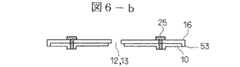
図6−aは、本実施例の変形例における、上フレーム1の突出部16を表面側(液晶表示パネルの表示面側)から見た模式図、図6−bは、図6−aのA−A切断線に沿った断面図である。
図6に示す変形例では、上フレーム1の突出部16に、凸部53を設け、当該凸部53により、下フレーム3の取り付け部10と上フレーム1の突出部16を位置決めし、これにより、上フレーム1と下フレーム3とを位置決めするようにしたものである。
なお、図6では、凸部52は、上フレーム1の突出部16の周囲の一部に形成しているが、この凸部53は、上フレーム1の突出部16の周囲の全てに形成してもよい。
図7−aは、本実施例の変形例における、上フレーム1の突出部16を表面側(液晶表示パネルの表示面側)から見た模式図、図7−bは、図7−aのA−A切断線に沿った断面図である。
図7に示す変形例では、下フレーム3の取り付け部10に、凸部55を設け、当該凸部55により、下フレーム3の取り付け部10と上フレーム1の突出部16を位置決めし、これにより、上フレーム1と下フレーム3とを位置決めするようにしたものである。
なお、図7では、凸部55は、下フレーム3の取り付け部10の周囲の一部に形成しているが、この凸部55は、下フレーム3の取り付け部10の周囲の全てに形成してもよい。FIG. 5 is a cross-sectional view showing a modification of the present embodiment. FIG. 5 is a cross-sectional view of the same portion as FIG.
In the modification shown in FIG. 5, a
6A is a schematic view of the protruding
In the modification shown in FIG. 6, a protruding
In FIG. 6, the
FIG. 7A is a schematic view of the
In the modified example shown in FIG. 7, the mounting
In FIG. 7, the
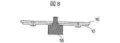
図8は、本実施例の変形例を示す断面図である。
本実施例では、治具56を使用し、始めに、治具56に下フレーム3の取り付け部10に設けた孔12を挿入し、その後、治具56に上フレーム1の突出部16に設けた孔13を挿入して、液晶表示モジュールを組み立てるものである。
治具56は、下フレーム3の取り付け部10に設けた孔12の直径に一致する部分と、上フレーム1の突出部16に設けた孔13の直径に一致する部分とを有するので、本方法によっても、上フレーム1と下フレーム3とを位置決めすることができる。
なお、前述の各実施例では、本発明を液晶表示モジュールに適用した実施例について説明したが、本発明はこれに限定されるものではなく、本発明は、有機EL素子、あるいは無機EL素子を用いるEL表示パネルを使用する表示装置にも適用可能であることはいうまでもない。
以上、本発明者によってなされた発明を、前記実施例に基づき具体的に説明したが、本発明は、前記実施例に限定されるものではなく、その要旨を逸脱しない範囲において種々変更可能であることは勿論である。FIG. 8 is a cross-sectional view showing a modification of the present embodiment.
In this embodiment, the
Since the
In each of the above-described embodiments, the embodiment in which the present invention is applied to the liquid crystal display module has been described. However, the present invention is not limited to this, and the present invention includes an organic EL element or an inorganic EL element. Needless to say, the present invention is also applicable to a display device using the EL display panel to be used.
As mentioned above, the invention made by the present inventor has been specifically described based on the above embodiments. However, the present invention is not limited to the above embodiments, and various modifications can be made without departing from the scope of the invention. Of course.
1 上フレーム
2 液晶表示パネル
3 下フレーム
5 回路基板(Tcon)のカバー
6 ラベル
7 直下型バックライト(BL)のモールド
10 取り付け部
11 連結部
12,13 孔
15 側壁
16 突出部(または、フランジ)
20 ソケット
21,22 ケーブル
25 ネジ
30 リアマウント用の取り付け部
31a,31b,31c,31d 連結部
32 ネジ穴
51,52,53,55 凸部
56 治具
BL バックライト
DPCB ドレイン回路基板
GPCB ゲート回路基板
DTCP,GTCP テープキャリアパッケージ
DFPC,GFPCフレキシブル回路基板
Tcon 回路基板
DESCRIPTION OF
20
Claims (3)
Translated fromJapanese前記表示パネルの表示面側に配置され、金属からなる上フレームと、
前記表示パネルの表示面と反対側に配置され、金属からなる下フレームとを有し、
前記下フレームは、前記上フレームに固定される表示装置であって、
前記下フレームは、前記表示パネルの表示面の裏面側に位置する本体部と、
前記表示パネルの外側に突出し、当該表示装置を筐体に取り付けるための孔を有する取り付け部と、
前記本体部と前記取り付け部とを連結する複数の連結部とを有し、
前記本体部と前記表示パネル間の電気部品用のケーブルが、前記複数の連結部の間から引き出されていることを特徴とする表示装置。A display panel;
An upper frame made of metal and disposed on the display surface side of the display panel;
The display surface of the display panel and arranged on the oppositeside,and a lower frame consisting ofmetals,
The lower frame is a display devicefixed to the upper frame ,
The lower frame is a main body located on the back side of the display surface of the display panel;
A mounting portion that protrudes outside the display panel and has a hole for mounting the display device to the housing;
Have a plurality of connecting portions for connecting the mounting portion and the bodyportion,
Display cables for the electrical components between the display panel and the main body portion, characterized that youhave withdrawn from between the plurality of connecting portions.
前記上フレームの前記突出部と、前記下フレームの前記取り付け部とは、ネジで固定されていることを特徴とする請求項1または請求項2に記載の表示装置。The upper frame has a protruding portion that protrudes to the outside of the display panel;
The display device according to claim 1, wherein the protruding portion of the upper frame and the attachment portion of the lower frame are fixed with screws.
Priority Applications (3)
| Application Number | Priority Date | Filing Date | Title |
|---|---|---|---|
| JP2003318308AJP4642332B2 (en) | 2003-09-10 | 2003-09-10 | Display device |
| US10/934,692US20050052587A1 (en) | 2003-09-10 | 2004-09-07 | Display device |
| CNA2004100737531ACN1595246A (en) | 2003-09-10 | 2004-09-09 | Display device |
Applications Claiming Priority (1)
| Application Number | Priority Date | Filing Date | Title |
|---|---|---|---|
| JP2003318308AJP4642332B2 (en) | 2003-09-10 | 2003-09-10 | Display device |
Related Child Applications (1)
| Application Number | Title | Priority Date | Filing Date |
|---|---|---|---|
| JP2010207744ADivisionJP2011028284A (en) | 2010-09-16 | 2010-09-16 | Display |
Publications (2)
| Publication Number | Publication Date |
|---|---|
| JP2005156575A JP2005156575A (en) | 2005-06-16 |
| JP4642332B2true JP4642332B2 (en) | 2011-03-02 |
Family
ID=34225319
Family Applications (1)
| Application Number | Title | Priority Date | Filing Date |
|---|---|---|---|
| JP2003318308AExpired - Fee RelatedJP4642332B2 (en) | 2003-09-10 | 2003-09-10 | Display device |
Country Status (3)
| Country | Link |
|---|---|
| US (1) | US20050052587A1 (en) |
| JP (1) | JP4642332B2 (en) |
| CN (1) | CN1595246A (en) |
Families Citing this family (9)
| Publication number | Priority date | Publication date | Assignee | Title |
|---|---|---|---|---|
| CN100397170C (en)* | 2003-10-16 | 2008-06-25 | 明基电通股份有限公司 | Flat panel display and panel module thereof |
| JP5382486B2 (en)* | 2007-05-02 | 2014-01-08 | Nltテクノロジー株式会社 | Liquid crystal display |
| WO2009054177A1 (en)* | 2007-10-24 | 2009-04-30 | Sharp Kabushiki Kaisha | Illuminating device for display device, display device, and television receiver |
| CN101477264A (en)* | 2009-01-20 | 2009-07-08 | 深圳帝光电子有限公司 | LCD display screen |
| JP4621799B1 (en) | 2009-05-22 | 2011-01-26 | シャープ株式会社 | Light reflecting sheet, light source device and display device |
| JP4519944B1 (en) | 2009-05-22 | 2010-08-04 | シャープ株式会社 | Light source device and display device |
| JP5351723B2 (en)* | 2009-05-22 | 2013-11-27 | シャープ株式会社 | Light source device and display device |
| JP5877318B2 (en)* | 2010-09-28 | 2016-03-08 | パナソニックIpマネジメント株式会社 | Display device |
| JP2019109385A (en)* | 2017-12-19 | 2019-07-04 | シャープ株式会社 | Display device |
Family Cites Families (10)
| Publication number | Priority date | Publication date | Assignee | Title |
|---|---|---|---|---|
| JPH01171479U (en)* | 1988-05-16 | 1989-12-05 | ||
| JPH0427424U (en)* | 1990-06-27 | 1992-03-04 | ||
| JP3562027B2 (en)* | 1995-04-21 | 2004-09-08 | ソニー株式会社 | Electronics |
| JP3486531B2 (en)* | 1997-08-08 | 2004-01-13 | キヤノン株式会社 | Liquid crystal device |
| US6501641B1 (en)* | 1998-10-23 | 2002-12-31 | Lg. Philips Lcd Co. Ltd. | Portable computer having a flat panel display device |
| JP2001337611A (en)* | 2000-03-22 | 2001-12-07 | Furukawa Electric Co Ltd:The | Display frame |
| KR100412106B1 (en)* | 2001-01-04 | 2003-12-24 | 삼성전자주식회사 | Flat panel display |
| JP2002268566A (en)* | 2001-03-12 | 2002-09-20 | Fujitsu Ltd | Display panel module |
| JP3577698B2 (en)* | 2001-08-03 | 2004-10-13 | 日本航空電子工業株式会社 | Liquid crystal display |
| JP3789401B2 (en)* | 2002-06-24 | 2006-06-21 | Nec液晶テクノロジー株式会社 | Liquid crystal module and liquid crystal monitor using the same |
- 2003
- 2003-09-10JPJP2003318308Apatent/JP4642332B2/ennot_activeExpired - Fee Related
- 2004
- 2004-09-07USUS10/934,692patent/US20050052587A1/ennot_activeAbandoned
- 2004-09-09CNCNA2004100737531Apatent/CN1595246A/enactivePending
Also Published As
| Publication number | Publication date |
|---|---|
| JP2005156575A (en) | 2005-06-16 |
| CN1595246A (en) | 2005-03-16 |
| US20050052587A1 (en) | 2005-03-10 |
Similar Documents
| Publication | Publication Date | Title |
|---|---|---|
| CN101393329B (en) | A kind of device and its manufacturing method | |
| CN1249648C (en) | Display module and display unit | |
| US7667798B2 (en) | Liquid crystal display device | |
| US8704972B2 (en) | Connector for light source module and backlight assembly having the same | |
| US7264480B2 (en) | Display device | |
| WO2006126376A1 (en) | Liquid crystal display | |
| KR20160082556A (en) | Display Device | |
| JP2008304913A (en) | Storage container, liquid crystal display device including the same, and method of assembling the same | |
| US7425133B2 (en) | Display device | |
| KR20100138181A (en) | LCD Display | |
| JP5523228B2 (en) | Display device and manufacturing method thereof | |
| CN104094335B (en) | Display device and television receiving device | |
| JP4642332B2 (en) | Display device | |
| CN107664863B (en) | Liquid crystal display device having a plurality of pixel electrodes | |
| EP2503381A1 (en) | Liquid crystal display device | |
| US20050219807A1 (en) | Portable multi-display device | |
| KR101255279B1 (en) | Backlight Unit | |
| JP2009294377A (en) | Display and television receiver | |
| JP2003177379A (en) | Liquid crystal display | |
| JP2862900B2 (en) | LCD display | |
| JP2011028284A (en) | Display | |
| KR20080000848A (en) | Liquid crystal display module | |
| US20070291511A1 (en) | Cables fixing apparatus for backlight module | |
| KR20070121164A (en) | Liquid crystal display module | |
| JP3599348B2 (en) | Liquid crystal display |
Legal Events
| Date | Code | Title | Description |
|---|---|---|---|
| A621 | Written request for application examination | Free format text:JAPANESE INTERMEDIATE CODE: A621 Effective date:20060904 | |
| A977 | Report on retrieval | Free format text:JAPANESE INTERMEDIATE CODE: A971007 Effective date:20100204 | |
| A131 | Notification of reasons for refusal | Free format text:JAPANESE INTERMEDIATE CODE: A131 Effective date:20100209 | |
| A521 | Request for written amendment filed | Free format text:JAPANESE INTERMEDIATE CODE: A523 Effective date:20100412 | |
| A131 | Notification of reasons for refusal | Free format text:JAPANESE INTERMEDIATE CODE: A131 Effective date:20100720 | |
| A521 | Request for written amendment filed | Free format text:JAPANESE INTERMEDIATE CODE: A523 Effective date:20100916 | |
| TRDD | Decision of grant or rejection written | ||
| A01 | Written decision to grant a patent or to grant a registration (utility model) | Free format text:JAPANESE INTERMEDIATE CODE: A01 Effective date:20101130 | |
| A01 | Written decision to grant a patent or to grant a registration (utility model) | Free format text:JAPANESE INTERMEDIATE CODE: A01 | |
| A61 | First payment of annual fees (during grant procedure) | Free format text:JAPANESE INTERMEDIATE CODE: A61 Effective date:20101201 | |
| R150 | Certificate of patent or registration of utility model | Ref document number:4642332 Country of ref document:JP Free format text:JAPANESE INTERMEDIATE CODE: R150 Free format text:JAPANESE INTERMEDIATE CODE: R150 | |
| FPAY | Renewal fee payment (event date is renewal date of database) | Free format text:PAYMENT UNTIL: 20131210 Year of fee payment:3 | |
| FPAY | Renewal fee payment (event date is renewal date of database) | Free format text:PAYMENT UNTIL: 20131210 Year of fee payment:3 | |
| S111 | Request for change of ownership or part of ownership | Free format text:JAPANESE INTERMEDIATE CODE: R313115 Free format text:JAPANESE INTERMEDIATE CODE: R313121 | |
| FPAY | Renewal fee payment (event date is renewal date of database) | Free format text:PAYMENT UNTIL: 20131210 Year of fee payment:3 | |
| R350 | Written notification of registration of transfer | Free format text:JAPANESE INTERMEDIATE CODE: R350 | |
| R250 | Receipt of annual fees | Free format text:JAPANESE INTERMEDIATE CODE: R250 | |
| R250 | Receipt of annual fees | Free format text:JAPANESE INTERMEDIATE CODE: R250 | |
| R250 | Receipt of annual fees | Free format text:JAPANESE INTERMEDIATE CODE: R250 | |
| R250 | Receipt of annual fees | Free format text:JAPANESE INTERMEDIATE CODE: R250 | |
| R250 | Receipt of annual fees | Free format text:JAPANESE INTERMEDIATE CODE: R250 | |
| R250 | Receipt of annual fees | Free format text:JAPANESE INTERMEDIATE CODE: R250 | |
| R250 | Receipt of annual fees | Free format text:JAPANESE INTERMEDIATE CODE: R250 | |
| R250 | Receipt of annual fees | Free format text:JAPANESE INTERMEDIATE CODE: R250 | |
| S531 | Written request for registration of change of domicile | Free format text:JAPANESE INTERMEDIATE CODE: R313531 | |
| S533 | Written request for registration of change of name | Free format text:JAPANESE INTERMEDIATE CODE: R313533 | |
| R350 | Written notification of registration of transfer | Free format text:JAPANESE INTERMEDIATE CODE: R350 | |
| R250 | Receipt of annual fees | Free format text:JAPANESE INTERMEDIATE CODE: R250 | |
| LAPS | Cancellation because of no payment of annual fees |