JP4640880B2 - Microprocessor system - Google Patents
Microprocessor systemDownload PDFInfo
- Publication number
- JP4640880B2 JP4640880B2JP2000213697AJP2000213697AJP4640880B2JP 4640880 B2JP4640880 B2JP 4640880B2JP 2000213697 AJP2000213697 AJP 2000213697AJP 2000213697 AJP2000213697 AJP 2000213697AJP 4640880 B2JP4640880 B2JP 4640880B2
- Authority
- JP
- Japan
- Prior art keywords
- processor
- processors
- microprocessor system
- vliw
- control unit
- Prior art date
- Legal status (The legal status is an assumption and is not a legal conclusion. Google has not performed a legal analysis and makes no representation as to the accuracy of the status listed.)
- Expired - Fee Related
Links
Images


Landscapes
- Executing Machine-Instructions (AREA)
- Multi Processors (AREA)
- Microcomputers (AREA)
- Power Sources (AREA)
- Advance Control (AREA)
Description
Translated fromJapanese【0001】
【発明の属する技術分野】
本発明はマイクロプロセッサシステム、特に、1チップ・マイクロプロセッサシステムに関する。
【0002】
【従来の技術及び発明が解決しようとする課題】
近年、マルチメディア分野の進展が著しく、1チップ・マイクロプロセッサへの市場ニーズが高まっている。このマルチメディア分野では、音声、画像、通信等の多くのアプリケーション機能が要求されるが、これらのすべてのアプリケーション機能を従来1チップ・マイクロプロセッサとして用いられてきた縮小命令セットコンピュータ(RISC)型プロセッサにオンチップすることはチップ面積、製造コスト等の観点から困難であり、アーキテクチャ上性能に限界が出始めている。従って、これを打破するために、RISC型プロセッサのアーキテクチャの改善または変更が要求されている。しかしながら、上のRISC型プロセッサの改善または変更はRISC市場でのソフトウエアの互換性を維持できず、機能、サービスの迅速なアップグレードが不可能であるという課題がある。
【0003】
他方、マルチメディア分野では、特に、グラフィックス、画像処理等の高速化が要求されると共にマルチメディア分野が一般家庭にも普及していくものである。従って、マルチメディア分野の1チップ・マイクロプロセッサは高性能にもかかわらず、低消費電力に対する期待が大きい。従来、消費電力を低減するために、1チップ・マイクロプロセッサの動作クロック周波数を単に低下させることにより1チップ・マイクロプロセッサを構成するCMOS回路活性化率を低減させることが行われているが(参照:特開平8−272579号公報)、この場合、処理性能が低下するという課題がある。
【0004】
従って、本発明の目的は、従来のソフトウエアの互換性を維持しつつ、機能、サービスの迅速なアップグレードを可能にするマイクロプロセッサシステムを提供することにある。
【0005】
【課題を解決するための手段】
上述の課題を解決するために本発明に係るマイクロプロセッサシステムにおいては、少なくともシステム全体を管理するために少なくとも基本ソフトを実行する第1のプロセッサと、所定の処理を実行するために少なくともアプリケーションソフトの各プログラムを格納して各プログラムを実行する複数の第2のプロセッサと、第1のプロセッサと複数の第2のプロセッサとの間に接続されたプロセッサ接続ユニットと、複数の第2のプロセッサに格納された各プログラムを必要に応じて書替えるための、第1のプロセッサと内部データバスを介して複数の第2のプロセッサのそれぞれとを接続する専用線とを設ける。プロセッサ接続ユニットは、第1のプロセッサのデータ信号及び各第2のプロセッサのデータ信号の分配を行う分配手段と、第1のプロセッサの制御信号に応じて複数の第2のプロセッサの全部もしくは一部を起動させるためのプロセッサ制御ユニットとを具備する。この結果、各第2のプロセッサに独立の処理を行わせることにより動作クロック周波数を高めることなく処理性能を高めることができる。また、第1のプロセッサの互換性を維持できる。たとえば、第1のプロセッサは基本ソフト及びアプリケーションソフトの各プログラムの一部を実行し、各第2のプロセッサはアプリケーションソフトの各プログラムの残りの部分を実行する。
【0006】
プロセッサ制御ユニットは各第2のプロセッサの動作クロック周波数及び/または電圧電源を独立に制御する。これにより、消費電力を高めることなく処理性能を高めることができる。
【0007】
プロセッサ制御ユニットは第1のプロセッサのサブルーチンコール命令を用いて各第2のプロセッサを起動させる。これにより、第1のプロセッサの互換性を維持できる。
【0009】
さらに、第1のプロセッサはRISC型プロセッサであり、各第2のプロセッサはVLIW型プロセッサである。この結果、RISC型プロセッサの互換性を維持できる。
【0010】
複数の第2のプロセッサは並列モード、パイプラインモードもしくはスローダウンモードにより動作する。スローダウンモードにより消費電力の低減が図られる。
【0011】
さらに、第1のプロセッサ、第2のプロセッサ及びプロセッサ接続ユニットに接続された内部バスを設け、第1のプロセッサ、第2のプロセッサ及びプロセッサ接続ユニットに対して内部バスよりデータを格納せしめるようにした。たとえば、アプリケーションソフトを第2のプロセッサにダウンロードさせることにより、機能、サービスのアップグレードが可能となる。
【0012】
また、マイクロプロセッサシステムは1チップにより構成した。さらに、第2のプロセッサはアプリケーションソフトを格納する揮発性または不揮発性メモリを有する。不揮発性メモリとしてはROM、強誘電体メモリ等を用いる。
【0013】
【発明の実施の形態】
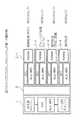
図1は本発明に係る1チップ・マイクロプロセッサシステムの実施の形態を示すブロック回路図である。
図1において、1はシステム全体を管理するためのRISC型プロセッサ、2−1、2−2、2−3、2−4は所定の処理を実行するためのVLIW(Very Long Instruction Word)型プロセッサ、3はRISC型プロセッサ1の出力に応じてVLIW型プロセッサ2−1、2−2、2−3、2−4の全部もしくは一部を起動させるためのプロセッサ接続ユニットである。尚、各VLIW型プロセッサ2−1、2−2、2−3、2−4はコンパイラが処理の依存性を調べた上で長い固定長たとえば128ビットの命令を作るものであり、この場合、この命令は複数の処理から構成されているが、実行時に命令の依存関係を調べる必要はない。
【0014】
また、RISC型プロセッサ1、VLIW型プロセッサ2−1、2−2、2−3、2−4及びプロセッサ接続ユニット3は内部データバス4に接続されており、さらに、内部データバス4は外部データバス5に接続されている。
【0015】
RISC型プロセッサ1は内部データバス4を介して命令入力専用信号Iにより命令を入力し、他方、内部データバス4を介してデータ入出力信号D0によりデータ入出力を行う。従って、RISC型プロセッサ1は上述の命令を解読してVLIW型プロセッサ2−1、2−2、2−3、2−4を制御するための制御信号C0を発生する。この結果、プロセッサ接続ユニット3は、各VLIW型プロセッサ2−1、2−2、2−3、2−4に対して制御信号C1、C2、C3、C4、動作クロック周波数500MHz、250MHz、125MHzあるいは0MHzのクロック信号CK1、CK2、CK3、CK4、及び5V、3Vあるいは0Vの電源電圧V1、V2、V3、V4を発生する。他方、RISC型プロセッサ1により演算処理されたデータはデータ信号D1によりプロセッサ接続ユニット3を介してデータ信号D31、D32、D33、D34によりVLIW型プロセッサ2−1、2−2、2−3、2−4に供給される。
【0016】
さらに、各VLIW型プロセッサ2−1、2−2、2−3、2−4に対してプログラム入力信号PI1、PI2、PI3、PI4を入力することによりアプリケーションプログラムが各VLIW型プロセッサ2−1、2−2、2−3、2−4に格納される。
【0017】
図2は図1のRISC型プロセッサの詳細なブロック回路図である。命令用キャッシュメモリ101は命令入力専用信号Iにより入力された命令を格納する。命令制御ユニット102は命令用キャッシュメモリ101より命令を読出して解読し、この結果、命令制御ユニット102は制御信号C1、C2、C3、C4、クロック信号CK1、CK2、CK3、CK4及び電源電圧V1、V2、V3、V4を発生すると共に、解読結果を演算ユニット103に供給する。演算ユニット103は解読結果に応じて所定の演算を行い、その際、データ用キャッシュメモリ104のデータ及びプロセッサ接続ユニット3からのデータ信号D1を入力する。尚、データ用キャッシュメモリ104は内部データバス4に接続されている。
【0018】
図3は図1のVLIW型プロセッサ2−i(i=1,2,3,4)の詳細なブロック回路図である。図3において、VLIW型プロセッサの2−i全体は電源電圧Viの下でクロック信号CKiの動作クロック周波数で動作する。命令制御ユニット201はプロセッサ制御ユニット3から制御信号Ciを受信してアクセス信号Aをプログラムメモリ202に送信する。この結果、プログラムメモリ202から命令信号ISにより命令が読み出され、この命令は命令制御ユニット201によって解読される。さらに、この解読結果に基づいて演算ユニット203がデータ信号D3iのデータに対して所定の演算を実行する。
尚、各VLIW型プロセッサ2−iのプログラムメモリ202にはプログラム入力信号PIiにより必要なプログラムが書込まれる。この場合、プログラムメモリ202をリアルタイムで書替えることにより最適なプログラム構成が可能である。また、プログラムメモリ202をDRAM、SRAM等の揮発性メモリで構成することができるが、強誘電体メモリ(FeRAM)等の不揮発性メモリでも構成できる。この場合、システム立上がり時間を少なくでき、しかもシステムの立上げのプログラムロードがないので低電力消費にも貢献できる。
【0019】
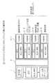
図4は図1のプロセッサ接続ユニット3の詳細なブロック回路図である。図4において、プロセッサ接続ユニット3は、レジスタ群301、データバッファ302、ポート303及びVLIW制御ユニット304により構成されている。RISC型プロセッサ1から制御信号C0はVLIW制御ユニット304に供給され、この結果、VLIW制御ユニット304は制御信号 C1、C2、C3、C4、クロック信号CK1、CK2、CK3、CK4及び電源電圧V1、V2、V3、V4を発生する。また、RISC型プロセッサ1とのデータ信号D1、VLIW型プロセッサ2−1、2−2、2−3、2−4とのデータ信号D31、D32、D33、D34及びデータバッファ302とのデータ信号D4により、これらの間のデータはポート303によって分配される。さらに、データバッファ302はデータ信号D2により内部データバス4を介してRISC型プロセッサ1のデータ用キャッシュメモリ104及び外部データバス5との間でデータ転送を行う。この場合、ダイレクトメモリアクセス(DMA)等の高速データ転送方式を用いればより効果的なデータ転送が可能となる。
【0020】
図5はRISC型プロセッサ1に用いられるRISCプロセッサ命令のフォーマットを示す図である。図4のVLIW制御ユニット304はRISCプロセッサ命令のサブルーチン命令コードにより動作するように構成してあり、これにより、従来のソフトウエアとの互換性を維持する。すなわち、VLIW制御ユニット304はRISCプロセッサ命令のオペレーションコードがサブルーチン命令コードのときにVLIW制御信号を解読し、動作周波数番号、電源電圧番号、プログラム番号に応じて制御信号C1、C2、C3、C4、クロック信号CK1、CK2、CK3、CK4、電源電圧V1、V2、V3、V4を発生する。
【0021】
図6は図5のVLIW制御信号の例を示す。たとえば、VLIW制御信号が00000のときには、全VLIW型プロセッサ2−1、2−2、2−3、2−4を予め定めてある状態に初期化する。また、VLIW制御信号が00001〜10000のいずれかのときには、VLIW型プロセッサ2−1、2−2、2−3、2−4のクロック信号CK1、CK2、CK3またはCK4の周波数を動作周波数番号指定の周波数たとえば500MHz、250MHz、125MHzまたは0MHzに設定すると共に、VLIW型プロセッサ2−1、2−2、2−3又は2−4の電源電圧を電源電圧番号指定の電圧たとえば5V、3Vまたは0Vに設定する。なお、この場合、クロック信号CK1、CK2、CK3、CK4の周波数及び電源電圧V1、V2、V3、V4の最適な組合せを別個に設定することも可能である。
【0022】
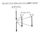
VLIW制御信号が10001〜10000のいずれかのときには、図7に示すごとく、VLIW型プロセッサ2−1、2−2、2−3、2−4のいずれかをプログラム番号指定のプログラム起動する。また、VLIW制御信号が10101のときには、図8に示すごとく、2つのVLIW型プロセッサたとえば2−1、2−3を起動する。さらに、VLIW制御信号が10110、10111のいずれかのときには、図9に示すごとく、全VLIW型プロセッサ2−1、2−2、2−3、2−4を起動する。たとえば、図9においては、RISC型プロセッサ1が主プログラムを実行すると、VLIW型プロセッサ2−1、2−2、2−3、2−4で実行するサブルーチンに同時にリンクする。これにより、VLIW型プロセッサ2−1、2−2、2−3、2−4の並列処理性が向上する。
【0023】
図10は図1のマイクロプロセッサシステムの第1の動作例を示すブロック回路図である。尚、図7において、DEC(DECoder)は命令制御ユニット、ALU(Arithmetic Logic Unit)、MAC (Multiplier / ACcumulator)は演算ユニット、FeRAM(強誘電体RAM)はプログラムメモリを示す。MPEG画像の再生たとえばDVDにおける再生においては、グラフィック処理、通信処理は不要である。この場合には、VLIW制御信号00001、01110、00011、10000により、クロック信号CK1、CK2、CK3、CK4を500MHz、0MHz、500MHz、0MHzに設定すると共に、電源電圧V1、V2、V3、V4を電圧5V、0V、5V、0Vに設定する。そして、VLIW制御信号10101によりVLIW型プロセッサ2−1、2−3の各プログラム番号指定のプログラムを起動する。
【0024】
図11は図1のマイクロプロセッサシステムの第2の動作例を示すブロック回路図である。すなわち、グラフィック処理、通信処理をも行う。この場合には、VLIW制御信号00001、00010、00011、00100により、クロック信号CK1、CK2、CK3、CK4を500MHz、500MHz、500MHz、500MHzに設定すると共に、電源電圧V1、V2、V3、V4を電圧5Vに設定する。そして、VLIW制御信号10110によりVLIW型プロセッサ2−1、2−2、2−3、2−4の各プログラム番号指定のプログラムを起動する。これにより、VLIW型プロセッサ2−1、2−2、2−3、2−4は、互いに独立した処理である画像処理(MPEG)、グラフィック処理(2D、3D)、音声処理(合成、認識)、通信処理を動作周波数500MHzで実行する。この場合、他の組合せでもよい。
【0025】
図12は図1のマイクロプロセッサシステムの第3の動作例を示すブロック回路図である。すなわち、グラフィック処理、通信処理をも行う。この場合には、VLIW制御信号01001、01010、01011、01100により、クロック信号CK1、CK2、CK3、CK4を125MHz、125MHz、125MHz、125MHzに設定すると共に、電源電圧V1、V2、V3、V4を電圧3Vに設定する。そして、VLIW制御信号10110によりVLIW型プロセッサ2−1、2−2、2−3、2−4の各プログラム番号指定のプログラムを起動する。これにより、VLIW型プロセッサ2−1、2−2、2−3、2−4は、互いに独立した処理である画像処理(MPEG)、グラフィック処理(2D,3D)、音声処理(合成、認識)、通信処理を動作周波数125MHzのスローダウンモードで実行する。この場合、他の組合せでもよい。
【0026】
図13は図1のマイクロプロセッサシステムの第4の動作例を示すブロック回路図である。すなわち、グラフィック処理、通信処理をも行う。この場合には、VLIW制御信号00001、00110、01011、01100により、クロック信号CK1、CK2、CK3、CK4を500MHz、500MHz、250MHz、125MHzに設定すると共に、電源電圧V1、V2、V3、V4を電圧5V、5V、3V、3Vに設定する。そして、VLIW制御信号10110によりVLIW型プロセッサ2−1、2−2、2−3、2−4の各プログラム番号指定のプログラムを起動する。これにより、VLIW型プロセッサ2−1、2−2、2−3、2−4は、最も負荷の重い画像処理(MPEG)、中程度の負荷のグラフィック処理(2D,3D)、最も負荷の軽い音声処理(合成、認識)及び通信処理を最適に実行する。この場合、他の組合せでもよい。この結果、チップ全体の消費電力に大きく寄与することになる。
【0027】
図14は図1のマイクロプロセッサシステムの第5の動作例を示すブロック回路図である。すなわち、VLIW制御信号00001、00010、00011、00100により、クロック信号CK1、CK2、CK3、CK4を500MHz、500MHz、500MHz、500MHzに設定すると共に、電源電圧V1、V2、V3、V4を電圧5Vに設定する。そして、VLIW制御信号10111によりVLIW型プロセッサ2−1、2−2、2−3、2−4の各プログラム番号指定のプログラムを起動する。これにより、VLIW型プロセッサ2−1、2−2、2−3、2−4は、特定処理たとえば高画像処理を細分化してこれをパイプライン処理する。細分化の例として、VLC(Variable Length Coding)、IQ(Inverse Quantization)、IDCT(Inverse Discrete Cosine Transform)、MC(Motion Compensation)の各処理を動作周波数500MHzで実行する。
【0028】
上述の実施の形態においては、RISC型プロセッサ1は基本ソフトを実行し、各VLIW型プロセッサ2−1、2−2、2−3、2−4はアプリケーションソフトの各プログラムを実行しているが、RISC型プロセッサ1は基本ソフト及びアプリケーションソフトの各プログラムの一部を実行し、各VLIWプロセッサ2−1、2−2、2−3、2−4はアプリケーションソフトの各プログラムの残り部分を実行するようにしてもよい。すなわち、アプリケーションソフトをRISC型プロセッサ1及び各VLIW型プロセッサ2−1、2−2、2−3、2−4間に分散させることによりアプリケーションソフトの変更に効率的に対処できる。
【0029】
【発明の効果】
以上説明したように本発明によれば、第1のプロセッサたとえばRISC型プロセッサに対して複数の第2のプロセッサたとえばVLIW型プロセッサを設けているので、第2のプロセッサにプログラムをダウンロードして機能、サービスをアップグレードさせてもソフトウエアの互換性を維持できる。また、第2のプロセッサを独立に動作させるので、消費電力を低減できる。
【図面の簡単な説明】
【図1】本発明に係る1チップ・マイクロプロセッサシステムの実施の形態を示すブロック回路図である。
【図2】図1のRISC型プロセッサの詳細なブロック回路図である。
【図3】図1のVLIW型プロセッサの詳細なブロック回路図である。
【図4】図1のプロセッサ接続ユニットの詳細なブロック回路図である。
【図5】図1のRISC型プロセッサに用いられるRISCプロセッサ命令のフォーマットを示す図である。
【図6】図5のVLIW制御番号の例を示す図である。
【図7】図1のマイクロプロセッサシステムの動作を示すシーケンス図である。
【図8】図1のマイクロプロセッサシステムの動作を示すシーケンス図である。
【図9】図1のマイクロプロセッサシステムの動作を示すシーケンス図である。
【図10】図1のマイクロプロセッサシステムの第1の動作例を示すブロック回路図である。
【図11】図1のマイクロプロセッサシステムの第2の動作例を示すブロック回路図である。
【図12】図1のマイクロプロセッサシステムの第3の動作例を示すブロック回路図である。
【図13】図1のマイクロプロセッサシステムの第4の動作例を示すブロック回路図である。
【図14】図1のマイクロプロセッサシステムの第5の動作例を示すブロック回路図である。
【符号の説明】
1…RISC型プロセッサ
2−1、2−2、2−3、2−4…VLIW型プロセッサ
3…プロセッサ接続ユニット
101…命令用キャッシュメモリ
102…命令制御ユニット
103…演算ユニット
104…データ用キャッシュメモリ
201…命令用キャッシュメモリ
202…プログラムメモリ
203…演算ユニット
I…命令入力信号
D0…データ入力信号
D1、D2、D31、D32、D33、D34…データ信号
C0、C1、C2、C3、C4…制御信号
CK1、CK2、CK3、CK4…クロック信号
V1、V2、V3、V4…電源電圧
PI1、PI2、PI3、PI4…プログラム入力信号
A…アクセス信号
IS…命令信号[0001]
BACKGROUND OF THE INVENTION
The present invention relates to a microprocessor system, and more particularly to a one-chip microprocessor system.
[0002]
[Prior art and problems to be solved by the invention]
In recent years, the multimedia field has made remarkable progress, and the market needs for a one-chip microprocessor have increased. In this multimedia field, many application functions such as voice, image, communication and the like are required, but all these application functions are conventionally used as a reduced-chip set computer (RISC) type processor as a one-chip microprocessor. However, it is difficult to on-chip from the viewpoint of chip area, manufacturing cost, and the like, and there is a limit on performance in terms of architecture. Therefore, there is a need to improve or change the RISC processor architecture to overcome this. However, the improvement or modification of the above RISC type processor cannot maintain software compatibility in the RISC market, and there is a problem that a rapid upgrade of functions and services is impossible.
[0003]
On the other hand, in the multimedia field, in particular, speeding up of graphics, image processing, and the like is required, and the multimedia field is spreading to general households. Therefore, a one-chip microprocessor in the multimedia field has high expectations for low power consumption despite its high performance. Conventionally, in order to reduce the power consumption, the activation rate of the CMOS circuit constituting the one-chip microprocessor is reduced by simply lowering the operation clock frequency of the one-chip microprocessor (see reference). In this case, there is a problem that the processing performance is deteriorated.
[0004]
SUMMARY OF THE INVENTION Accordingly, an object of the present invention is to provide a microprocessor system that enables rapid upgrade of functions and services while maintaining compatibility of conventional software.
[0005]
[Means for Solving the Problems]
In order to solve the above-described problems, in the microprocessor system according to the present invention, at leasta first processorthat executes at least basic software for managing the entire system, and atleast application software for executing predetermined processing. A plurality of second processorsfor storing each program and executing each program,a processor connection unitconnected between the first processorand the plurality of second processors, and aplurality of second processors A dedicated line for connecting the first processor and each of the plurality of second processors via the internal data bus is provided for rewriting each program as necessary .The processor connection unit distributes the data signal of the first processor and the data signal of each second processor, and all or a part of the plurality of second processors according to the control signal of the first processor And a processor control unit for starting up. As a result, the processing performance can be improved without increasing the operation clock frequency by causing each second processor to perform independent processing.In addition, the compatibility of the first processor can be maintained. For example, the first processor executes a part of each program of basic software and application software, and each second processor executes the remaining part of each program of application software.
[0006]
The processorcontrol unit independently controls the operating clock frequency and / or voltage power supply of each second processor. Thereby, processing performance can be improved without increasing power consumption.
[0007]
The processorcontrol unit activates each second processor using a subroutine call instruction of the first processor. Thereby, the compatibility of the first processor can be maintained.
[0009]
Further, the first processor is a RISC type processor, and each second processor is a VLIW type processor. As a result, the compatibility of the RISC type processor can be maintained.
[0010]
The plurality of second processors operate in a parallel mode, a pipeline mode, or a slow down mode. The power consumption can be reduced by the slow down mode.
[0011]
Furthermore, an internal bus connected to the first processor, the second processor, and the processor connection unit is provided so that the first processor, the second processor, and the processor connection unit can store data from the internal bus. . For example, it is possible to upgrade functions and services by downloading application software to the second processor.
[0012]
The microprocessor system is composed of one chip. Further, the second processor has a volatile or non-volatile memory for storing application software. As the nonvolatile memory, a ROM, a ferroelectric memory, or the like is used.
[0013]
DETAILED DESCRIPTION OF THE INVENTION
FIG. 1 is a block circuit diagram showing an embodiment of a one-chip microprocessor system according to the present invention.
In FIG. 1, 1 is a RISC type processor for managing the entire system, and 2-1, 2-2, 2-3, 2-4 are VLIW (Very Long Instruction Word) type processors for executing predetermined processing.
[0014]
The
[0015]
The
[0016]
Furthermore, the program input signal PI1, PI2, PI3, the VLIW type processor application program by entering the PI4 2-1 for each VLIW typeprocessor 2-1, 2-2, 2-3, 2-4, 2-2, 2-3, 2-4.
[0017]
FIG. 2 is a detailed block circuit diagram of the RISC type processor of FIG. The
[0018]
FIG. 3 is a detailed block circuit diagram of the VLIW processor 2-i (i = 1, 2, 3, 4) of FIG. In FIG. 3, the entire 2-LI of the VLIW processor operates at the operation clock frequency of the clock signal CKi under the power supply voltage Vi. The
A necessary program is written in the
[0019]
FIG. 4 is a detailed block circuit diagram of the
[0020]
Figure 5 is a diagram showing a format of a RISC processor instruction usedin the
[0021]
FIG. 6 shows an example of the VLIW control signal of FIG. For example, when the VLIW control signal is 00000, all VLIW processors 2-1, 2-2, 2-3, 2-4 are initialized to a predetermined state. When the VLIW control signal is any of 00001 to 10000, the frequency of the clock signal CK1, CK2, CK3 or CK4 of the VLIW type processor 2-1, 2-2, 2-3, 2-4 is designated as the operation frequency number. The frequency is set to 500 MHz, 250 MHz, 125 MHz, or 0 MHz, and the power supply voltage of the VLIW processor 2-1, 2-2, 2-3, or 2-4 is set to the voltage specified by the power supply voltage number, for example, 5V, 3V, or 0V. Set. In this case, the optimum combination of the frequencies of the clock signals CK1, CK2, CK3, and CK4 and the power supply voltages V1, V2, V3, and V4 can be set separately.
[0022]
When the VLIW control signal is any one of 10001 to 10000, as shown in FIG. 7, any one of the VLIW type processors 2-1, 2-2, 2-3,2-4 is activated with a program number designated. When the VLIW control signal is10101 , as shown in FIG. 8, two VLIW processors such as 2-1, 2-3 are started. Further, when the VLIW control signal is10110 or10111 , as shown in FIG. 9, all the VLIW type processors 2-1, 2-2, 2-3,2-4 are activated. For example, in FIG. 9, when the
[0023]
FIG. 10 is a block circuit diagram showing a first operation example of the microprocessor system of FIG. In FIG. 7, DEC (DECoder) indicates an instruction control unit, ALU (Arithmetic Logic Unit), MAC (Multiplier / ACcumulator) indicates an arithmetic unit, and FeRAM (ferroelectric RAM) indicates a program memory. In the reproduction of MPEG images, for example, reproduction on a DVD, graphic processing and communication processing are unnecessary. In this case, the clock signals CK1, CK2, CK3, and CK4 are set to 500 MHz, 0 MHz, 500 MHz, and 0 MHz by the VLIW control signals 00001, 01110, 0101, and 10000, and the power supply voltages V1, V2, V3, and V4 are set to voltages. Set to 5V, 0V, 5V, 0V. Then, each program number designation program of the VLIW type processors 2-1 and 2-3 is activated by the VLIW control signal10101 .
[0024]
FIG. 11 is a block circuit diagram showing a second operation example of the microprocessor system of FIG. That is, graphic processing and communication processing are also performed. In this case, the clock signals CK1, CK2, CK3, and CK4 are set to 500 MHz, 500 MHz, 500 MHz, and 500 MHz by the VLIW control signals 00001, 00010, 0101, and 00100, and the power supply voltages V1, V2, V3, and V4 are set to voltages. Set to 5V. Then, each program number designation program of the VLIW type processors 2-1, 2-2, 2-3, 2-4 is activated by the VLIW control signal10110 . As a result, the VLIW processors 2-1, 2-2, 2-3, 2-4 can perform image processing (MPEG), graphic processing (2D, 3D), and audio processing (synthesis, recognition), which are independent processes. The communication process is executed at an operating frequency of 500 MHz. In this case, other combinations may be used.
[0025]
FIG. 12 is a block circuit diagram showing a third operation example of the microprocessor system of FIG. That is, graphic processing and communication processing are also performed. In this case, the clock signals CK1, CK2, CK3, and CK4 are set to 125 MHz, 125 MHz, 125 MHz, and 125 MHz by the VLIW control signals 01001, 01010, 01011, and 01100, and the power supply voltages V1, V2, V3, and V4 are set to voltages. Set to 3V. Then, each program number designation program of the VLIW type processors 2-1, 2-2, 2-3, 2-4 is activated by the VLIW control signal10110 . As a result, the VLIW type processors 2-1, 2-2, 2-3, 2-4 can perform independent image processing (MPEG), graphic processing (2D, 3D), and audio processing (synthesis, recognition). The communication process is executed in a slow down mode with an operating frequency of 125 MHz. In this case, other combinations may be used.
[0026]
FIG. 13 is a block circuit diagram showing a fourth operation example of the microprocessor system of FIG. That is, graphic processing and communication processing are also performed. In this case, the clock signals CK1, CK2, CK3, and CK4 are set to 500 MHz, 500 MHz, 250 MHz, and 125 MHz by the VLIW control signals 00001, 00110, 01011, and 01100, and the power supply voltages V1, V2, V3, and V4 are set to voltages. Set to5V, 5V, 3V, 3V. Then, each program number designation program of the VLIW type processors 2-1, 2-2, 2-3, 2-4 is activated by the VLIW control signal10110 . As a result, the VLIW type processors 2-1, 2-2, 2-3, 2-4 have the highest load image processing (MPEG), medium load graphic processing (2D, 3D), and the lightest load. Voice processing (synthesis, recognition) and communication processing are optimally executed. In this case, other combinations may be used. As a result, it greatly contributes to the power consumption of the entire chip.
[0027]
FIG. 14 is a block circuit diagram showing a fifth operation example of the microprocessor system of FIG. That is, the clock signals CK1, CK2, CK3, and CK4 are set to 500 MHz, 500 MHz, 500 MHz, and 500 MHz, and the power supply voltages V1, V2, V3, and V4 are set to the
[0028]
In the above-described embodiment, the
[0029]
【The invention's effect】
As described above, according to the present invention, since a plurality of second processors such as VLIW processors are provided for the first processor such as the RISC processor, the program is downloaded to the second processor and functions. Software compatibility can be maintained even if the service is upgraded. Further, since the second processor is operated independently, power consumption can be reduced.
[Brief description of the drawings]
FIG. 1 is a block circuit diagram showing an embodiment of a one-chip microprocessor system according to the present invention.
FIG. 2 is a detailed block circuit diagram of the RISC type processor of FIG. 1;
FIG. 3 is a detailed block circuit diagram of the VLIW type processor of FIG. 1;
FIG. 4 is a detailed block circuit diagram of the processor connection unit of FIG. 1;
FIG. 5 is a diagram showing a format of a RISC processor instruction used in the RISC type processor of FIG. 1;
6 is a diagram illustrating an example of a VLIW control number in FIG. 5;
FIG. 7 is a sequence diagram showing an operation of the microprocessor system of FIG. 1;
FIG. 8 is a sequence diagram showing an operation of the microprocessor system of FIG. 1;
FIG. 9 is a sequence diagram showing an operation of the microprocessor system of FIG. 1;
FIG. 10 is a block circuit diagram showing a first operation example of the microprocessor system of FIG. 1;
FIG. 11 is a block circuit diagram showing a second operation example of the microprocessor system of FIG. 1;
12 is a block circuit diagram showing a third operation example of the microprocessor system of FIG. 1; FIG.
FIG. 13 is a block circuit diagram showing a fourth operation example of the microprocessor system of FIG. 1;
FIG. 14 is a block circuit diagram showing a fifth operation example of the microprocessor system of FIG. 1;
[Explanation of symbols]
DESCRIPTION OF
Claims (15)
Translated fromJapanese所定の処理を実行するために少なくともアプリケーションソフトの各プログラムを格納して該各プログラムを実行する複数の第2のプロセッサ(2−1、2−2、2−3、2−4)と、
前記第1のプロセッサと前記複数の第2のプロセッサとの間に接続されたプロセッサ接続ユニット(3)と、
前記複数の第2のプロセッサに格納された前記各プログラムを必要に応じて書替えるための、前記第1のプロセッサと内部データバス(4)を介して前記複数の第2のプロセッサのそれぞれとを接続する専用線(PIi)と
を具備し、
前記プロセッサ接続ユニットは、
前記第1のプロセッサのデータ信号及び前記各第2のプロセッサのデータ信号の分配を行う分配手段(303)と、
前記第1のプロセッサの制御信号に応じて前記複数の第2のプロセッサの全部もしくは一部を起動させるためのプロセッサ制御ユニット(304)と
を具備するマイクロプロセッサシステム。A first processor (1) that executes at least basic software to manage at least the entire system;
A plurality of second processors (2-1, 2-2, 2-3, 2-4) for storing at least each program of the application software and executing each program in order to execute a predetermined process;
A processor connection unit (3) connected between the first processor and the plurality of second processors;
The first processor and each of the plurality of second processors via the internal data bus (4) for rewriting the respective programs stored in the plurality of second processors as necessary. A dedicated line (PIi) to be connected ,
The processor connection unitis :
Distribution means (303) for distributing the data signal of the first processor and the data signal of each of the second processors;
A microprocessor system comprising: a processor control unit (304) for activating all or a part of the plurality of second processors in response to a control signal of the first processor.
前記第1のプロセッサ、前記第2のプロセッサ及び前記プロセッサ接続ユニットに接続された内部バス(4)を具備し、前記第1のプロセッサ、前記第2のプロセッサ及び前記プロセッサ接続ユニットに対して前記内部バスよりデータを格納せしめるようにした請求項1に記載のマイクロプロセッサシステム。further,
An internal bus (4) connected to the first processor, the second processor, and the processor connection unit, the internal bus (4) connected to the first processor, the second processor, and the processor connection unit; 2. The microprocessor system according to claim 1, wherein data is stored from the bus.
Priority Applications (1)
| Application Number | Priority Date | Filing Date | Title |
|---|---|---|---|
| JP2000213697AJP4640880B2 (en) | 2000-07-14 | 2000-07-14 | Microprocessor system |
Applications Claiming Priority (1)
| Application Number | Priority Date | Filing Date | Title |
|---|---|---|---|
| JP2000213697AJP4640880B2 (en) | 2000-07-14 | 2000-07-14 | Microprocessor system |
Publications (2)
| Publication Number | Publication Date |
|---|---|
| JP2002032218A JP2002032218A (en) | 2002-01-31 |
| JP4640880B2true JP4640880B2 (en) | 2011-03-02 |
Family
ID=18709408
Family Applications (1)
| Application Number | Title | Priority Date | Filing Date |
|---|---|---|---|
| JP2000213697AExpired - Fee RelatedJP4640880B2 (en) | 2000-07-14 | 2000-07-14 | Microprocessor system |
Country Status (1)
| Country | Link |
|---|---|
| JP (1) | JP4640880B2 (en) |
Families Citing this family (12)
| Publication number | Priority date | Publication date | Assignee | Title |
|---|---|---|---|---|
| US6526491B2 (en) | 2001-03-22 | 2003-02-25 | Sony Corporation Entertainment Inc. | Memory protection system and method for computer architecture for broadband networks |
| US7516334B2 (en) | 2001-03-22 | 2009-04-07 | Sony Computer Entertainment Inc. | Power management for processing modules |
| US7093104B2 (en) | 2001-03-22 | 2006-08-15 | Sony Computer Entertainment Inc. | Processing modules for computer architecture for broadband networks |
| US7231500B2 (en) | 2001-03-22 | 2007-06-12 | Sony Computer Entertainment Inc. | External data interface in a computer architecture for broadband networks |
| US7233998B2 (en) | 2001-03-22 | 2007-06-19 | Sony Computer Entertainment Inc. | Computer architecture and software cells for broadband networks |
| US6826662B2 (en) | 2001-03-22 | 2004-11-30 | Sony Computer Entertainment Inc. | System and method for data synchronization for a computer architecture for broadband networks |
| US6809734B2 (en) | 2001-03-22 | 2004-10-26 | Sony Computer Entertainment Inc. | Resource dedication system and method for a computer architecture for broadband networks |
| EP1662376A4 (en) | 2003-08-07 | 2009-02-18 | Panasonic Corp | PROCESSOR INTEGRATED CIRCUIT AND PRODUCT DEVELOPING METHOD USING THE CIRCUIT |
| US8224639B2 (en) | 2004-03-29 | 2012-07-17 | Sony Computer Entertainment Inc. | Methods and apparatus for achieving thermal management using processing task scheduling |
| US20050262311A1 (en)* | 2004-05-20 | 2005-11-24 | Lippincott Louis A | Hierarchical processor architecture for video processing |
| JP2009140304A (en) | 2007-12-07 | 2009-06-25 | Sony Corp | Semiconductor chip |
| JP5565228B2 (en) | 2010-09-13 | 2014-08-06 | ソニー株式会社 | Processor |
Family Cites Families (7)
| Publication number | Priority date | Publication date | Assignee | Title |
|---|---|---|---|---|
| JPH02306333A (en)* | 1989-05-22 | 1990-12-19 | Mitsubishi Electric Corp | Printing controller |
| JPH0514495A (en)* | 1991-07-03 | 1993-01-22 | Fujitsu Ltd | Extension test method for line control unit |
| JPH07271740A (en)* | 1994-03-30 | 1995-10-20 | Hitachi Ltd | Program description method and information processing apparatus |
| JPH09106388A (en)* | 1995-10-11 | 1997-04-22 | Oki Electric Ind Co Ltd | Parallel computer for signal processing |
| JP3623840B2 (en)* | 1996-01-31 | 2005-02-23 | 株式会社ルネサステクノロジ | Data processing apparatus and microprocessor |
| US5977997A (en)* | 1997-03-06 | 1999-11-02 | Lsi Logic Corporation | Single chip computer having integrated MPEG and graphical processors |
| JP3857052B2 (en)* | 1998-07-02 | 2006-12-13 | 株式会社ルネサステクノロジ | Microprocessor |
- 2000
- 2000-07-14JPJP2000213697Apatent/JP4640880B2/ennot_activeExpired - Fee Related
Also Published As
| Publication number | Publication date |
|---|---|
| JP2002032218A (en) | 2002-01-31 |
Similar Documents
| Publication | Publication Date | Title |
|---|---|---|
| JP4640880B2 (en) | Microprocessor system | |
| KR101061345B1 (en) | Video processing | |
| US7920584B2 (en) | Data processing system | |
| US6567426B1 (en) | Preemptive timer multiplexed shared memory access | |
| US5517665A (en) | System for controlling arbitration using the memory request signal types generated by the plurality of datapaths having dual-ported local memory architecture for simultaneous data transmission | |
| JP5677774B2 (en) | Digital signal processor | |
| EP1347391A2 (en) | System on chip | |
| US7724984B2 (en) | Image processing apparatus | |
| WO2007140428A2 (en) | Multi-threaded processor with deferred thread output control | |
| GB2311882A (en) | Data processing management system with programmable routing operations | |
| JPH0984004A (en) | Image processing device | |
| US11935153B2 (en) | Data compression support for accelerated processor | |
| US8495345B2 (en) | Computing apparatus and method of handling interrupt | |
| US5452101A (en) | Apparatus and method for decoding fixed and variable length encoded data | |
| Basoglu et al. | Single‐chip processor for media applications: the MAP1000™ | |
| KR101030174B1 (en) | Video Processing | |
| US20040193835A1 (en) | Table lookup instruction for processors using tables in local memory | |
| US7984204B2 (en) | Programmable direct memory access controller having pipelined and sequentially connected stages | |
| Stolberg et al. | HiBRID-SoC: A multi-core SoC architecture for multimedia signal processing | |
| Kurohmaru et al. | A MPEG4 programmable codec DSP with an embedded pre/post-processing engine | |
| JP2002182975A (en) | Multiprocessor system | |
| KR100450844B1 (en) | Video CODEC processor architecture | |
| KR100308118B1 (en) | Amplifier Audio Decoder | |
| Glaskowsky | Fujitsu aims media processor at DVD | |
| GB2425862A (en) | Data processing system |
Legal Events
| Date | Code | Title | Description |
|---|---|---|---|
| A621 | Written request for application examination | Free format text:JAPANESE INTERMEDIATE CODE: A621 Effective date:20070510 | |
| A711 | Notification of change in applicant | Free format text:JAPANESE INTERMEDIATE CODE: A711 Effective date:20071023 | |
| A711 | Notification of change in applicant | Free format text:JAPANESE INTERMEDIATE CODE: A711 Effective date:20071023 | |
| RD02 | Notification of acceptance of power of attorney | Free format text:JAPANESE INTERMEDIATE CODE: A7422 Effective date:20080408 | |
| A977 | Report on retrieval | Free format text:JAPANESE INTERMEDIATE CODE: A971007 Effective date:20090713 | |
| A131 | Notification of reasons for refusal | Free format text:JAPANESE INTERMEDIATE CODE: A131 Effective date:20090728 | |
| A521 | Request for written amendment filed | Free format text:JAPANESE INTERMEDIATE CODE: A523 Effective date:20090917 | |
| A131 | Notification of reasons for refusal | Free format text:JAPANESE INTERMEDIATE CODE: A131 Effective date:20100708 | |
| A521 | Request for written amendment filed | Free format text:JAPANESE INTERMEDIATE CODE: A523 Effective date:20100902 | |
| TRDD | Decision of grant or rejection written | ||
| A01 | Written decision to grant a patent or to grant a registration (utility model) | Free format text:JAPANESE INTERMEDIATE CODE: A01 Effective date:20101116 | |
| A01 | Written decision to grant a patent or to grant a registration (utility model) | Free format text:JAPANESE INTERMEDIATE CODE: A01 | |
| A61 | First payment of annual fees (during grant procedure) | Free format text:JAPANESE INTERMEDIATE CODE: A61 Effective date:20101125 | |
| R150 | Certificate of patent or registration of utility model | Free format text:JAPANESE INTERMEDIATE CODE: R150 | |
| FPAY | Renewal fee payment (event date is renewal date of database) | Free format text:PAYMENT UNTIL: 20131210 Year of fee payment:3 | |
| LAPS | Cancellation because of no payment of annual fees |