JP4639172B2 - Semiconductor device - Google Patents
Semiconductor deviceDownload PDFInfo
- Publication number
- JP4639172B2 JP4639172B2JP2006237361AJP2006237361AJP4639172B2JP 4639172 B2JP4639172 B2JP 4639172B2JP 2006237361 AJP2006237361 AJP 2006237361AJP 2006237361 AJP2006237361 AJP 2006237361AJP 4639172 B2JP4639172 B2JP 4639172B2
- Authority
- JP
- Japan
- Prior art keywords
- schottky
- substrate
- drain
- source
- semiconductor device
- Prior art date
- Legal status (The legal status is an assumption and is not a legal conclusion. Google has not performed a legal analysis and makes no representation as to the accuracy of the status listed.)
- Active
Links
Images


Classifications
- H—ELECTRICITY
- H10—SEMICONDUCTOR DEVICES; ELECTRIC SOLID-STATE DEVICES NOT OTHERWISE PROVIDED FOR
- H10D—INORGANIC ELECTRIC SEMICONDUCTOR DEVICES
- H10D62/00—Semiconductor bodies, or regions thereof, of devices having potential barriers
- H10D62/40—Crystalline structures
- H10D62/405—Orientations of crystalline planes
- H—ELECTRICITY
- H10—SEMICONDUCTOR DEVICES; ELECTRIC SOLID-STATE DEVICES NOT OTHERWISE PROVIDED FOR
- H10D—INORGANIC ELECTRIC SEMICONDUCTOR DEVICES
- H10D84/00—Integrated devices formed in or on semiconductor substrates that comprise only semiconducting layers, e.g. on Si wafers or on GaAs-on-Si wafers
- H10D84/01—Manufacture or treatment
- H10D84/0123—Integrating together multiple components covered by H10D12/00 or H10D30/00, e.g. integrating multiple IGBTs
- H10D84/0126—Integrating together multiple components covered by H10D12/00 or H10D30/00, e.g. integrating multiple IGBTs the components including insulated gates, e.g. IGFETs
- H10D84/0165—Integrating together multiple components covered by H10D12/00 or H10D30/00, e.g. integrating multiple IGBTs the components including insulated gates, e.g. IGFETs the components including complementary IGFETs, e.g. CMOS devices
- H10D84/0167—Manufacturing their channels
- H—ELECTRICITY
- H10—SEMICONDUCTOR DEVICES; ELECTRIC SOLID-STATE DEVICES NOT OTHERWISE PROVIDED FOR
- H10D—INORGANIC ELECTRIC SEMICONDUCTOR DEVICES
- H10D84/00—Integrated devices formed in or on semiconductor substrates that comprise only semiconducting layers, e.g. on Si wafers or on GaAs-on-Si wafers
- H10D84/01—Manufacture or treatment
- H10D84/0123—Integrating together multiple components covered by H10D12/00 or H10D30/00, e.g. integrating multiple IGBTs
- H10D84/0126—Integrating together multiple components covered by H10D12/00 or H10D30/00, e.g. integrating multiple IGBTs the components including insulated gates, e.g. IGFETs
- H10D84/0165—Integrating together multiple components covered by H10D12/00 or H10D30/00, e.g. integrating multiple IGBTs the components including insulated gates, e.g. IGFETs the components including complementary IGFETs, e.g. CMOS devices
- H10D84/0188—Manufacturing their isolation regions
- H—ELECTRICITY
- H10—SEMICONDUCTOR DEVICES; ELECTRIC SOLID-STATE DEVICES NOT OTHERWISE PROVIDED FOR
- H10D—INORGANIC ELECTRIC SEMICONDUCTOR DEVICES
- H10D84/00—Integrated devices formed in or on semiconductor substrates that comprise only semiconducting layers, e.g. on Si wafers or on GaAs-on-Si wafers
- H10D84/01—Manufacture or treatment
- H10D84/0123—Integrating together multiple components covered by H10D12/00 or H10D30/00, e.g. integrating multiple IGBTs
- H10D84/0126—Integrating together multiple components covered by H10D12/00 or H10D30/00, e.g. integrating multiple IGBTs the components including insulated gates, e.g. IGFETs
- H10D84/0165—Integrating together multiple components covered by H10D12/00 or H10D30/00, e.g. integrating multiple IGBTs the components including insulated gates, e.g. IGFETs the components including complementary IGFETs, e.g. CMOS devices
- H10D84/0193—Integrating together multiple components covered by H10D12/00 or H10D30/00, e.g. integrating multiple IGBTs the components including insulated gates, e.g. IGFETs the components including complementary IGFETs, e.g. CMOS devices the components including FinFETs
- H—ELECTRICITY
- H10—SEMICONDUCTOR DEVICES; ELECTRIC SOLID-STATE DEVICES NOT OTHERWISE PROVIDED FOR
- H10D—INORGANIC ELECTRIC SEMICONDUCTOR DEVICES
- H10D84/00—Integrated devices formed in or on semiconductor substrates that comprise only semiconducting layers, e.g. on Si wafers or on GaAs-on-Si wafers
- H10D84/01—Manufacture or treatment
- H10D84/02—Manufacture or treatment characterised by using material-based technologies
- H10D84/03—Manufacture or treatment characterised by using material-based technologies using Group IV technology, e.g. silicon technology or silicon-carbide [SiC] technology
- H10D84/038—Manufacture or treatment characterised by using material-based technologies using Group IV technology, e.g. silicon technology or silicon-carbide [SiC] technology using silicon technology, e.g. SiGe
- H—ELECTRICITY
- H10—SEMICONDUCTOR DEVICES; ELECTRIC SOLID-STATE DEVICES NOT OTHERWISE PROVIDED FOR
- H10D—INORGANIC ELECTRIC SEMICONDUCTOR DEVICES
- H10D84/00—Integrated devices formed in or on semiconductor substrates that comprise only semiconducting layers, e.g. on Si wafers or on GaAs-on-Si wafers
- H10D84/01—Manufacture or treatment
- H10D84/02—Manufacture or treatment characterised by using material-based technologies
- H10D84/05—Manufacture or treatment characterised by using material-based technologies using Group III-V technology
- H—ELECTRICITY
- H10—SEMICONDUCTOR DEVICES; ELECTRIC SOLID-STATE DEVICES NOT OTHERWISE PROVIDED FOR
- H10D—INORGANIC ELECTRIC SEMICONDUCTOR DEVICES
- H10D84/00—Integrated devices formed in or on semiconductor substrates that comprise only semiconducting layers, e.g. on Si wafers or on GaAs-on-Si wafers
- H10D84/01—Manufacture or treatment
- H10D84/02—Manufacture or treatment characterised by using material-based technologies
- H10D84/08—Manufacture or treatment characterised by using material-based technologies using combinations of technologies, e.g. using both Si and SiC technologies or using both Si and Group III-V technologies
- H—ELECTRICITY
- H10—SEMICONDUCTOR DEVICES; ELECTRIC SOLID-STATE DEVICES NOT OTHERWISE PROVIDED FOR
- H10D—INORGANIC ELECTRIC SEMICONDUCTOR DEVICES
- H10D84/00—Integrated devices formed in or on semiconductor substrates that comprise only semiconducting layers, e.g. on Si wafers or on GaAs-on-Si wafers
- H10D84/80—Integrated devices formed in or on semiconductor substrates that comprise only semiconducting layers, e.g. on Si wafers or on GaAs-on-Si wafers characterised by the integration of at least one component covered by groups H10D12/00 or H10D30/00, e.g. integration of IGFETs
- H10D84/82—Integrated devices formed in or on semiconductor substrates that comprise only semiconducting layers, e.g. on Si wafers or on GaAs-on-Si wafers characterised by the integration of at least one component covered by groups H10D12/00 or H10D30/00, e.g. integration of IGFETs of only field-effect components
- H10D84/83—Integrated devices formed in or on semiconductor substrates that comprise only semiconducting layers, e.g. on Si wafers or on GaAs-on-Si wafers characterised by the integration of at least one component covered by groups H10D12/00 or H10D30/00, e.g. integration of IGFETs of only field-effect components of only insulated-gate FETs [IGFET]
- H10D84/85—Complementary IGFETs, e.g. CMOS
- H10D84/856—Complementary IGFETs, e.g. CMOS the complementary IGFETs having different architectures than each other, e.g. high-voltage and low-voltage CMOS
- H—ELECTRICITY
- H10—SEMICONDUCTOR DEVICES; ELECTRIC SOLID-STATE DEVICES NOT OTHERWISE PROVIDED FOR
- H10D—INORGANIC ELECTRIC SEMICONDUCTOR DEVICES
- H10D86/00—Integrated devices formed in or on insulating or conducting substrates, e.g. formed in silicon-on-insulator [SOI] substrates or on stainless steel or glass substrates
- H10D86/01—Manufacture or treatment
- H—ELECTRICITY
- H10—SEMICONDUCTOR DEVICES; ELECTRIC SOLID-STATE DEVICES NOT OTHERWISE PROVIDED FOR
- H10D—INORGANIC ELECTRIC SEMICONDUCTOR DEVICES
- H10D86/00—Integrated devices formed in or on insulating or conducting substrates, e.g. formed in silicon-on-insulator [SOI] substrates or on stainless steel or glass substrates
- H10D86/201—Integrated devices formed in or on insulating or conducting substrates, e.g. formed in silicon-on-insulator [SOI] substrates or on stainless steel or glass substrates the substrates comprising an insulating layer on a semiconductor body, e.g. SOI
- H—ELECTRICITY
- H10—SEMICONDUCTOR DEVICES; ELECTRIC SOLID-STATE DEVICES NOT OTHERWISE PROVIDED FOR
- H10D—INORGANIC ELECTRIC SEMICONDUCTOR DEVICES
- H10D87/00—Integrated devices comprising both bulk components and either SOI or SOS components on the same substrate
- H—ELECTRICITY
- H10—SEMICONDUCTOR DEVICES; ELECTRIC SOLID-STATE DEVICES NOT OTHERWISE PROVIDED FOR
- H10D—INORGANIC ELECTRIC SEMICONDUCTOR DEVICES
- H10D30/00—Field-effect transistors [FET]
- H10D30/60—Insulated-gate field-effect transistors [IGFET]
- H10D30/62—Fin field-effect transistors [FinFET]
Landscapes
- Metal-Oxide And Bipolar Metal-Oxide Semiconductor Integrated Circuits (AREA)
- Thin Film Transistor (AREA)
- Electrodes Of Semiconductors (AREA)
- Insulated Gate Type Field-Effect Transistor (AREA)
Description
Translated fromJapanese本発明は、広く半導体製造に関するものである。とりわけ、金属と半導体とのソース/ドレイン接合を有する相補型金属酸化膜半導体(CMOS)装置の製造方法に関するものである。The present invention relates generally to semiconductor manufacturing. In particular, it relates to a method of manufacturing a complementary metal oxide semiconductor (CMOS) device having a source / drain junction between a metal and a semiconductor.
最近の装置において使用される通常の電気接触は、金属と半導体との接触である。使用される材料に依存して、この接触は、オーム接触または整流性接触になり得る。オーム接触は、電流の方向に関係なく、低電気抵抗を有する。整流性接触は、一方向には自由に電流を通すが、逆方向には電流障壁を有しているという点で、ダイオードのように動作する。こうしたいわゆるショットキー障壁は、電子が金属側から半導体側へ通過するのに必要な電位のことであり、金属と半導体との接触における電気的特性を決定する場合の、重要なパラメータである。A common electrical contact used in modern devices is a metal-semiconductor contact. Depending on the material used, this contact can be an ohmic contact or a rectifying contact. The ohmic contact has a low electrical resistance regardless of the direction of current. A rectifying contact operates like a diode in that it conducts current freely in one direction but has a current barrier in the opposite direction. Such a so-called Schottky barrier is an electric potential necessary for electrons to pass from the metal side to the semiconductor side, and is an important parameter when determining electrical characteristics in contact between the metal and the semiconductor.
近年、進歩した半導体デバイスは、MOSFETのソースおよび/またはドレインを形成するのに、金属と半導体とのシットキー接触を利用する。ショットキーのソース/ドレイン(S/D)を有するMOSFETは、多くのデバイスが45nmノードを超えるスケーリング目標を達成することに対し、多くの利点を有する。このS/Dの金属/シリサイド(シリコン化合物)構造は、低抵抗を有しており、原子的には急激に変化するものとなっている。この構造により、デバイス速度が速くなり、既存の不純物がドープされたS/D技術に対して、スケール上の有利性がでてくる。金属/シリサイドのS/Dは、チャネルに対してショットキー障壁を形成し、そのことが漏洩電流Ioffの低減をもたらす。ショットキーS/D技術により、チャネル領域において必要なドーパントが減少し、この結果、チャネル領域における移動度が高くなる。さらに、ショットキーS/Dの製法は、他の半導体製造技術と同様に、SOI上のCMOSや、歪(strained)Si技術や、金属ゲートおよび高誘電率(high-k)ゲート誘電体や、SiGe歪技術などを含む、現在最先端のCMOS技術を包含する可能性がある。In recent years, advanced semiconductor devices have utilized metal-semiconductor sit-key contacts to form MOSFET sources and / or drains. MOSFETs with Schottky source / drain (S / D) have many advantages over many devices achieving scaling goals beyond the 45 nm node. This metal / silicide (silicon compound) structure of S / D has a low resistance and changes abruptly atomically. This structure increases device speed and provides a scale advantage over existing impurity doped S / D technology. The metal / silicide S / D forms a Schottky barrier to the channel, which leads to a reduction in leakage current Ioff. The Schottky S / D technique reduces the required dopant in the channel region, resulting in higher mobility in the channel region. Furthermore, the Schottky S / D manufacturing method is similar to other semiconductor manufacturing technologies, such as CMOS on SOI, strained Si technology, metal gate and high-k gate dielectric, It may include current state-of-the-art CMOS technology, including SiGe strain technology.
こうした明確な利点があるにも拘らず、現在の製造方法とショットキーS/D技術とを融合するのに直面する多くの挑戦が続いている。例えば、ソース電極における大きなショットキー障壁は、ショットキーCMOSの駆動電流をかなり劣化する。この問題を解決するために、約0.2eVより低いショットキー障壁を有するソース接合部が必要である。NMOS用のErSiやPMOS用のPtSiのように、何種類かの新たな材料が、詳細に調べられた。しかしながら、このような材料の融合は、何時も成功するとは限らなかった。新材料は、ショットキーS/D方法が大量生産に到達できる前に、金属堆積や、シリサイデーションや、エッチングのような現存する各製造ステップの最適化をやり直すことが必要とされる。Despite these distinct advantages, many challenges continue to face fusing current manufacturing methods with Schottky S / D technology. For example, a large Schottky barrier at the source electrode significantly degrades the Schottky CMOS drive current. To solve this problem, a source junction having a Schottky barrier lower than about 0.2 eV is required. Several new materials have been investigated in detail, such as ErSi for NMOS and PtSi for PMOS. However, such fusion of materials has not always been successful. New materials are required to re-optimize existing manufacturing steps such as metal deposition, silicidation and etching before the Schottky S / D method can reach mass production.
これらの問題とその他の問題の観点から、ショットキーS/D製造方法を改良するための必要性が残されている。金属対半導体の電気的特性は、制御されなければならないが、新製造方法は、他の製造方法との融合の問題を、過剰なものにすべきではない。一つの前進的な方法は、現存する材料を用いた新規なショットキーS/D法を発展させることにあり、それにより従来の方法を阻害していた融合の問題を、最小限に抑えることができる。In view of these and other problems, there remains a need to improve the Schottky S / D manufacturing method. Although the electrical properties of metal-to-semiconductors must be controlled, the new manufacturing method should not overload the problem of integration with other manufacturing methods. One progressive method is to develop a new Schottky S / D method using existing materials, thereby minimizing the fusion problem that has hindered the traditional method. it can.
NMOSとPMOSのショットキー障壁を低くするために、ショットキーS/DのCMOSがハイブリッド基板を使用する本発明の好ましい実施例により、これらと他の問題は、概ね解決または回避されて、技術的利点が広く達成される。In order to lower the NMOS and PMOS Schottky barriers, the preferred embodiment of the present invention in which a Schottky S / D CMOS uses a hybrid substrate, these and other problems are largely solved or avoided, and Benefits are widely achieved.
本発明の好ましい実施例において、半導体デバイスが提供される。この半導体デバイスは、第1の領域と第2の領域とを有し、前記第1の領域は、{110}の第1の結晶方位を有すると共に、前記第2の領域は、{211}の第2の結晶方位を有する基板と、前記第1の領域上に形成され、NMOSソースおよびNMOSドレインを有し、前記NMOSソースと前記NMOSドレインの少なくとも一つが類似ショットキー接触部を有するNMOSFETと、前記第2の領域上に形成され、PMOSソースおよびPMOSドレインを有し、前記PMOSソースと前記PMOSドレインの少なくとも一つが類似ショットキー接触部を有するPMOSFETと、を備えている。In a preferred embodiment of the present invention, a semiconductor device is provided. The semiconductor device hasa first region and a second region, the first region has a first crystal orientation of {110}, and the second region has {211} A substrate having a second crystal orientation; an NMOSFET formed on the first region, having an NMOS source and an NMOS drain, wherein at least one of the NMOS source and the NMOS drain has a similar Schottky contact; And a PMOSFET formed on the second region, having a PMOS source and a PMOS drain, wherein at least one of the PMOS source and the PMOS drain has a similar Schottky contact .
前述の説明は、以下に続く本発明の詳細な説明を理解し易くするために、本発明の特徴と技術の要点をむしろ概略的に述べたものである。以下、本発明とその他の特徴および技術を説明するが、これは本発明における各請求項の主題を成すものである。開示された着想と特定の実施例は、本発明と同様の目的を実行するために、別な構造とプロセスを一部変更または設計するための基礎として、容易に利用可能であることを当業者は理解するであろう。また、このような均等な構造は、添付の請求項に説明されているごとく、本発明の精神と範囲を逸脱するものではないことを、当業者は理解するであろう。The foregoing has outlined rather broadly the features and technical scope of the present invention in order that the detailed description of the invention that follows may be better understood. The present invention and other features and techniques will now be described, which form the subject of the claims of the present invention. It will be appreciated by those skilled in the art that the disclosed concepts and specific embodiments can be readily used as a basis for modifying or designing other structures and processes in part to carry out similar objectives to the present invention. Will understand. Those skilled in the art will also appreciate that such equivalent constructions do not depart from the spirit and scope of the invention as set forth in the appended claims.
本発明と、それによる利点をより完全に理解するために、添付図面と関連して、以下の記述が参照される。特に指示がない限り、異なる各図における同一番号および同一符号を、同一部分に対し引用する。各図は好ましい実施例に関連する態様を明確に示すのに描かれているが、一定の尺度に描かれる必要はない。For a more complete understanding of the present invention and the advantages thereby, reference is made to the following description, taken in conjunction with the accompanying drawings, in which: Unless otherwise indicated, the same reference numerals and symbols in different drawings are used for the same parts. Although the figures are drawn to clearly illustrate the aspects associated with the preferred embodiment, they need not be drawn to scale.
現在の好ましい実施例における製造と使用法を、以下に詳細に説明する。但し本発明は、多岐にわたる特定の状況において具体化される多くの利用可能な進歩性を提供するものであることが、十分に理解すべきである。検討される特定の実施例は、本発明を製造し使用するための特定の方法の単なる説明に過ぎず、本発明の範囲を限定するものではない。The manufacture and use in the presently preferred embodiment is described in detail below. However, it should be appreciated that the present invention provides many available inventive steps that may be embodied in a wide variety of specific situations. The specific embodiments discussed are merely illustrative of specific ways to make and use the invention, and do not limit the scope of the invention.
金属が半導体と接触する場合、金属と半導体との界面(interface)に障壁が形成される。この障壁(若しくは、障壁高さ)は、金属と半導体との間の仕事関数の差分と、界面準位密度と、半導体のドーピングレベルと、によって決定される。表面準位が無い場合は、障壁高さは主に、金属と半導体との間の仕事関数の差分で決定される。表面準位の密度が高い場合は、障壁高さが半導体の表面準位で決定され、金属の仕事関数と無関係となる。半導体の表面に高い表面準位の密度が存在する場合は、フェルミ準位が表面準位により固定されて、障壁高さは、これらの極限値の間にある。電子またはホールに対する障壁高さは、約0.4eVよりは高くないことが好ましい。When the metal contacts the semiconductor, a barrier is formed at the metal-semiconductor interface. This barrier (or barrier height) is determined by the work function difference between the metal and the semiconductor, the interface state density, and the doping level of the semiconductor. When there is no surface level, the barrier height is mainly determined by the work function difference between the metal and the semiconductor. When the density of surface states is high, the barrier height is determined by the surface state of the semiconductor and is independent of the work function of the metal. If a high surface level density exists on the surface of the semiconductor, the Fermi level is fixed by the surface level, and the barrier height is between these extreme values. The barrier height for electrons or holes is preferably not higher than about 0.4 eV.
表面準位の密度は、表面の結晶方位に大いに依存している。シリコンにおいて、{100}方位の表面準位密度は、{111}方位よりも約1オーダー小さい(すなわち、10倍小さい)。表面準位密度に影響を与えるとして知られている一つの要因は、シリコン表面における単位面積当りの原子結合数である。The density of surface states is highly dependent on the crystal orientation of the surface. In silicon, the surface state density in the {100} orientation is about one order smaller (ie, 10 times smaller) than the {111} orientation. One factor known to affect surface state density is the number of atomic bonds per unit area on the silicon surface.
本発明は、特定の状況、すなわちハイブリット基板上のCMOS製造における好ましい実施例に関して説明する。この実施例では、基板方位によって、NMOSとPMOSの双方に対し、低いショットキー障壁を可能にする。通常は、ショットキーダイオード、或いはショットキー障壁接合という言葉が技術的に使用されるが、便宜上、ここでは半導体に接着された金属で構成される構造を、ショットキー接触と称することにする。ここで使用されるように、いわゆるショットキー障壁は、金属/半導体の界面のことを言う。The present invention will be described with respect to a preferred situation in a particular situation, namely CMOS fabrication on a hybrid substrate. In this embodiment, the substrate orientation allows a low Schottky barrier for both NMOS and PMOS. Usually, the term “Schottky diode” or “Schottky barrier junction” is technically used, but for convenience, a structure composed of a metal bonded to a semiconductor is referred to as a Schottky contact. As used herein, a so-called Schottky barrier refers to a metal / semiconductor interface.
一般的に、USLI回路における基本的構成要素は、CMOS論理ゲートであり、これは少なくとも一個のNFETと、少なくとも一個のPFETとにより構成される。PFETとNFETに対し異なる結晶方位を持ち、それにより最適なホールと電子の移動度を与えるCMOS論理ゲートを実装するために、シリコン・オン・インシュレータ基板を用いられる。デバイスは、トライゲート(trigate)またはFinFETのように、プレーナまたは複数ゲートデバイスの何れかである。好ましい実施例における一つの利点は、キャリアの移動度が増加する場合は、論理ゲートの実際の面積(estate)が減少することである。従って、キャリアの移動度を向上させるのに、結晶方位を最適化することにより、半導体チップ全体における有効な実際の面積が節約される。さらに、製造コストが効果的に低減する。好ましい実施例のもう一つの利点は、フローティング・ボディー・エフェクトが緩和されることである。In general, the basic component in a USLI circuit is a CMOS logic gate, which consists of at least one NFET and at least one PFET. Silicon-on-insulator substrates are used to implement CMOS logic gates that have different crystal orientations for PFETs and NFETs, thereby providing optimal hole and electron mobility. The device is either a planar or multi-gate device, such as a trigate or FinFET. One advantage in the preferred embodiment is that the actual area of the logic gate decreases when the carrier mobility increases. Therefore, by optimizing the crystal orientation to improve carrier mobility, the effective actual area of the entire semiconductor chip is saved. Furthermore, the manufacturing cost is effectively reduced. Another advantage of the preferred embodiment is that the floating body effect is mitigated.
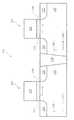
図1Aから図1Hまでを参照すると、本発明の好ましい実施例による製造手順が説明されている。図1Aから図1Hは、ここに引用される従来技術に基づいて、ウェハがシリコン基板に既に固着されている標準的なシリコン・オン・インシュレータ(SOI)構造の断面図を示している。SOI構造は、約2nmから200nmの間の厚さのシリコン層を有しているが、約40nmの厚さが好ましい。この発明の好ましい実施例では、図1は、選択された第1表面方位とドーピングレベルとを有するシリコン基板202を備えている。埋め込まれた誘電体(酸化)層であるBOX204が基板の上部を覆っている。BOX204は、約10nmから200nmの間の厚さを有しているが、約50nmが好ましい。選択された第2の表面方位とドーピングレベルとを有するSOIシリコン基板206が、BOX204の上部を覆っている。そして最後に、窒化物である硬質マスク層208が、SOIシリコン基板206の上部を覆っている。これに代わる実施例は、図示してはいないが、Ge,SiC,GaAs,GaAlAs,InP,GaN SiGe,SiGeの段階的なバッファーのような、バルク基板を含有する。ハイブリッド基板は、{100}および{110}のような、或る方位を有する部分を含んでもよい。さらに、BOX204は、例えば窒化シリコンのような酸化物以外の誘電体で構成してもよい。Referring to FIGS. 1A through 1H, a manufacturing procedure according to a preferred embodiment of the present invention will be described. 1A through 1H show cross-sectional views of a standard silicon-on-insulator (SOI) structure in which a wafer is already secured to a silicon substrate, according to the prior art cited herein. The SOI structure has a silicon layer with a thickness between about 2 nm and 200 nm, with a thickness of about 40 nm being preferred. In a preferred embodiment of the invention, FIG. 1 comprises a
次の図1Bにおいて、フォトレジスト層210が塗布され、パターン化され、そして現像される。図1Cにおいて、硬質マスク層208と第2のシリコン基板206とを貫通して、開口部212が形成される。図1Dにおいて、開口部212は、アクティブ領域を電気的に絶縁するために、SiO2などの絶縁物214で充填され、短絡接触を回避する。In the next FIG. 1B, a
次の図1eにおいて、第2のフォトレジスト層216が塗布される。第2のフォトレジスト層216は、図1fにおいて、パターン化およびエッチングされ、絶縁物214の選択された部分を貫通して、開口部218が形成される。図1fにおいて、ステップ後に残っている絶縁物214の部分は、浅溝分離すなわちSTIとして機能し、完成したデバイスの領域220となる。In the next FIG. 1e, a
次の図1Gにおいて、シリコンのエピタキシャル層222が、シリコン基板202上で成長する。このエピタキシャル層222の結晶方位は、基板202と同じである。次に、図1Gに示す多層構造が平坦化され、それによりデバイス製造に適した多結晶方位を有する基板を形成する。In the next FIG. 1G, an
種々の実施例を説明する場合に、結晶技術において通常使用される専門用語と学術用語を利用するのが、ここでは有益である。例えば、周知のミラー指数は、ここでは結晶の面と方向の説明に使用される。ここに開示した好ましい実施例はシリコンを含むので、当業者であれば、ミラー指数が面心立体結晶構造を引用していることを認識するであろう。結晶学の学術用語を尊守すれば、[xyz]と(xyz)は、それぞれ特定の方向と面を表現し、<xyz>と{xyz}は、それぞれ方向と面の一般的なタイプすなわち群(family)を表現する。例えば、[-1,0,1],[0,1,1],[1,-1,0],および[1,0,1]は、<1,1,0>の方向群における特定の各方向である。当業者ならば、特定のミラー指数を参照して実施例を説明することが、時には有益であることも認識するであろう。しかしながら、文脈からして明らかでない限り、特定の方向と面を参照することは、典型的な利便性と明確性のみに対するものである。同様に位置されたタイプの他の部材を参照することが、同様に適切であるような時には、単一の結晶方位または単一の方位に実施例を限定する意図は無い。In describing various embodiments, it is useful here to make use of technical and scientific terms commonly used in crystal technology. For example, the well-known Miller index is used here to describe the plane and orientation of the crystal. Since the preferred embodiment disclosed herein includes silicon, those skilled in the art will recognize that the Miller index refers to a face-centered cubic crystal structure. In keeping with the crystallographic terminology, [xyz] and (xyz) represent specific directions and planes, respectively, and <xyz> and {xyz} are general types or groups of directions and planes, respectively. (Family) is expressed. For example, [-1, 0, 1], [0, 1, 1], [1, -1, 0], and [1, 0, 1] are specified in the <1, 1, 0> direction group. In each direction. Those skilled in the art will also recognize that it is sometimes useful to describe an embodiment with reference to a particular Miller index. However, unless apparent from the context, references to specific directions and surfaces are for typical convenience and clarity only. There is no intention to limit embodiments to a single crystal orientation or a single orientation, as it is equally appropriate to refer to other members of a similarly located type.
さて、図2に目を向けると、好ましい実施例により形成されたCMOSデバイス250が説明されている。このCMOSデバイスは、PMOSFETハイブリット基板252上にあるPMOSFET251と、NMOSFETハイブリット基板256上にあるNMOSFET253とを備えている。異なるハイブリット領域は、STI258などによって絶縁される。ゲート誘電体259とゲート電極261が、CMOSデバイス250に含まれている。Turning now to FIG. 2, a
適切なゲート誘電体259は、ポリシリコンまたは完全なNiシリサイドのポリシリコンや、Al2O3,ZrO2,HfO2,Y2O3,La2O3,TiO2,Ta2O5などの金属酸化物や、ZrSiO4,ZrSiN,HfSiO4,HfSiON,HfSiNなどのシリケートや、SiO2などの酸化物や、オキシ窒化シリコンを含む。
適切なゲート電極261の材料は、Mo,Ru,Ti,Ta,W,またはHfから成る金属ゲートや、金属窒化物スタックゲートや、RuO2またはIrO2などの金属酸化物ゲートや、MoN,WN,TiN,TaN,TaAlN,TaSiNなどの金属窒化物ゲートや、ポリシリコンや、ポリSiGeゲートを含む。代わりの実施例において、CoSi2またはNiSiのようなゲートシリサイドを含んでもよい。Suitable materials for the
引き続き図2において、好ましい実施例のPMOSFET251は、ソース263とドレイン266を有し、このソース263とドレイン266は、ショットキー接触部を構成している。同様に、NMOSFET253は、ソース269とドレイン272を有し、このソース269とドレイン272は、ショットキー接触部を構成している。代わりの実施例では、図示してはいないが、PMOSFETのみ、或いは、NMOSFETのみが、ショットキー接触部を有していてもよい。さらに他の実施例では、図示してはいないが、ソースのみまたはドレインのみが、ショットキー接触部を有していてもよい。便宜上、ショットキーS/Dという用語は、ショットキー接触部から成るドレイン,ショットキー接触部から成るソース,またはこれらの組み合わせを引用するのに使用される。Continuing with FIG. 2, the
好ましくは、PMOSFETのハイブリット基板252は、{110}の方位を有し、NMOSFETのハイブリット基板256は{100}の方位を有している。{110}のシリコン基板上にショットキーS/DのPMOSFETを形成することは、この{110}がホールに対するショットキー障壁を最小にするという理由で、特に好ましい。同様に、{100}のシリコン基板上にショットキーS/DのNMOSFETを形成することは、この方位{100}が電子に対するショットキー障壁を最小にするという理由で、特に好ましい。このS/Dは、金属の堆積または金属シリサイドの堆積により形成され、好ましくは、N型とP型の各デバイスに対して、障壁の高さを低くするために、単一金属を使用して形成される。Preferably, the
基板で形成されたショットキー接触部は、ErSi,CoSi,NiSi,TiSi,WSi,PtSiのような耐熱性金属(refractory metal)シリサイドや、Mo,Ru,Ti,Ta,W,Hfのような耐熱性金属や、n型ドーパント(例えば、Li,Sb,P,As)や、p型ドーパント(例えば、B,Al,Ga,In)や、これらの組み合わせたものから成っている。好ましくは、これらの材料は、約4eV以上の大きさの仕事関数を有し、且つショットキー接触部(さもなければ、類似ショットキー接触部)として形成された場合には、約0.4eV未満のショットキー障壁高さを有する。ショットキー接触部は、500オングストローム未満の厚さであることが好ましい。The Schottky contact formed on the substrate is made of a refractory metal silicide such as ErSi, CoSi, NiSi, TiSi, WSi, and PtSi, or heat resistant such as Mo, Ru, Ti, Ta, W, and Hf. , An n-type dopant (for example, Li, Sb, P, As), a p-type dopant (for example, B, Al, Ga, In), or a combination thereof. Preferably, these materials have a work function greater than or equal to about 4 eV and less than about 0.4 eV when formed as a Schottky contact (otherwise a similar Schottky contact). Has a Schottky barrier height. The Schottky contact is preferably less than 500 angstroms thick.
表面準位に影響を与える上記の界面パラメータを考慮すると、本発明の代わりの実施例では、{i,j,k}から成るミラー指数群により表される結晶方位を有する基板上に形成されたNMOSFETと、{l,m,n}から成るミラー指数群により表される結晶方位を有する基板上に形成されたPMOSFETとを備え、l2+m2+n2>i2+j2+k2の関係にある。上記のように、特に好ましい実施例は、{110}の基板上に形成されたNMOSFETと、{100}の基板上に形成されたPMOSFETとから構成される。また代わりの実施例は、{110}または{100}の基板上に形成されたNMOSFETと、{111},{211},または{311}の基板上に形成されたPMOSFETと、から構成される。Considering the above interface parameters that affect the surface states, in an alternative embodiment of the present invention, it was formed on a substrate having a crystal orientation represented by a Miller index group consisting of {i, j, k}. An NMOSFET and a PMOSFET formed on a substrate having a crystal orientation represented by a Miller index group consisting of {l, m, n}, and a relationship of l2 + m2 + n2 > i2 + j2 + k2 is there. As noted above, a particularly preferred embodiment is comprised of an NMOSFET formed on a {110} substrate and a PMOSFET formed on a {100} substrate. An alternative embodiment comprises an NMOSFET formed on a {110} or {100} substrate and a PMOSFET formed on a {111}, {211}, or {311} substrate. .
図2についてさらに説明を続けると、さらに好ましい実施例において、PMOSFETチャネル275とNMOSFETチャネル278が、選択された結晶の方向に沿って向いている。従来のCMOS技術においては、単一の結晶方位を持った一つの特定の半導体基板上に、デバイスが形成されるのが一般的である。しかしながら、シリコン中において、電子は{100}の面群において最大の移動度を有し、ホールは{110}の面群において最大の移動度を有する。一般的に、PFETまたはNFETのどちらか一方が、その最適な結晶方位で使用され、他方は同じ結晶方位で使用されることが原因で、最適のキャリア移動度よりも低い移動度で動作する。ここで、キヌガワ氏の米国特許第4,857,986号公報を参考のために組み入れるが、結晶方位がキャリア移動度に与える影響に関して、いくつか記述している。研究者達はこれらの問題を認識し、複数の結晶方位を持つハイブリッド基盤上にCMOSを製造する技術を開発した。参考のためにここに組み入れたヨシカワ氏らの米国特許第4,857,986号公報には、ウェハボンディングと選択的エピタキシによって、(110)表面にPFETを製造し、(100)表面にNFETを製造する方法が記述されている。Continuing with FIG. 2, in a more preferred embodiment, the
これらのことを考慮して、PMOSFET251とNMOSFET253は、各キャリア濃度が最大となるハイブリッド基板の方位上に存在することが好ましい。(実施例に関連して上述したように、)それはキャリア移動度を最大化すると共に、ショットキー障壁の高さを最小化するので、このような構成は特に好ましい。さらに、好ましい実施例においては、電子移動度が{100}の方位に対して最大になる方向、すなわち<100>に沿って、NMOSFETのチャネル278を向ける。Considering these things, it is preferable that the
あまり好ましくない実施例(図示せず)において、PMOSFETチャネル275は、{110}の方位に対してホールの移動度が最大となる方向である<110>の方向に沿って向けられている。{110}<110>の構造が、あまり好ましくない理由は、{110}基板を包含する対称性を考慮してのことである。この方位においては、基板表面に平行な2つの<110>の方向だけが存在する。従って、{110}<110>の構造が、ハイブリッド基板の製造に際し、PMOSFETに対するデバイスレイアウトの選択度を減少させる。より好ましいPMOSFET251の構造は、図2で説明される。In a less preferred embodiment (not shown), the
図2に示すように、PMOSFETのチャネル275は、<111>の方向に沿って一致している。{110}<111>の基板/チャネル構造におけるホールの移動度は、最大値の約70%に過ぎないが、{110}の面では2つの<110>方向だけが存在するのに対して、この{110}の面では4つの<111>方向が存在する。これはすなわち、移動度が30%だけ減少する代わりに、PMOSFETにおけるデバイスレイアウトの選択度が2倍になることを意味する。従って、ショットキー障壁高さに関し、上述したものと同じ考慮を踏まえて、より好ましいPMOSFET251の方位が、図2で説明される。As shown in FIG. 2, the
上記に説明した実施例に加えて、本発明の代わりの実施例により、より高度なプレーナデバイスと、より高度な複合ゲートデバイスの製造方法を提供する。こうした代わりの実施例の一つを、図3に説明する。In addition to the embodiments described above, alternative embodiments of the present invention provide a more advanced planar device and a more advanced method of manufacturing a composite gate device. One such alternative embodiment is illustrated in FIG.
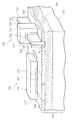
図3は、本発明の第1実施例を取り入れた半導体構造の部分に対する斜視図である。図3において、UTBSOIFETのようなプレーナトランジスタ330と、FinFETのような複合ゲートトランジスタ320を、セミコンダクタ・オン・インシュレータ(SOI)基板構造340上に形成したものが示されている。このSOI基板構造340は、基板342,絶縁層344,および半導体層364から構成される。プレーナトランジスタ330は、通常は薄く平板状の第1のアクティブ領域331を有する。複合ゲートトランジスタ320は、通常は背の高いフィン状の第2のアクティブ領域322を有する。第1のアクティブ領域331と第2のアクティブ領域322は、前記SOI構造340における同一の半導体層から形成される。第1のアクティブ領域331は第1の厚さt1を有し、第2のアクティブ領域322は第2の厚さt2を有する。第2の厚さcは、第1の厚さt1よりも厚い。FIG. 3 is a perspective view of a portion of the semiconductor structure incorporating the first embodiment of the present invention. In FIG. 3, a
第1の厚さt1は、約400オングストロームより薄いことが好ましく、約200オングストロームより薄いことがさらに好ましい。この第1の厚さt1は、プレーナトランジスタ330のゲート長さlgの半分より薄くてもよく、さらに好ましくは、第1の厚さt1は、ゲート長さlgの1/3よりも薄い。例えば、プレーナトランジスタ330のゲート長さlgが300オングストローム(30nm)の場合、第1の厚さt1は、150オングストロームより薄くてもよく、さらに好ましくは、100オングストロームよりも薄い。第1の厚さt1が、プレーナトランジスタ330のゲート長さlgの半分または1/3よりも薄い場合、当該プレーナトランジスタ330を、極薄状ボディ(UTB)トランジスタと称する。第1のゲート誘電体334は、第1のアクティブ領域331における第1のチャネル領域上に存在する。第1のゲート電極336は、第1のゲート誘電体334の上部に存在する。第1のゲート電極336の近傍に、プレーナトランジスタ330のソース337とドレイン338が、互いに対向して第1のアクティブ領域331に形成される。The first thickness t1 is preferably less than about 400 angstroms, and more preferably less than about 200 angstroms. This first thickness t1 may be less than half of the gate length lg of the
さらに、図3を参照すると、第2のアクティブ領域322のフィン構造の第2の厚さt2(すなわち、hf)は、例えば約100オングストロームよりも大きいことが好ましく、例えば約400オングストロームよりも大きいことがさらに好ましい。フィン幅wfは、約500オングストロームよりも大きいことが好ましい。第2のゲート誘電体324は、第2のアクティブ領域322における第2のチャネルの上に存在する。この第2のゲート誘電体324は、フィンの第2のチャネル領域の周囲を、少なくとも部分的に包んでいる。第2のゲート電極326は、第2のゲート誘電体324の上に存在する。第2のゲート誘電体324は、第2のアクティブ領域322のフィンから、第2のゲート電極326を電気的に絶縁する。図3に示す複合ゲートトランジスタ320は、トリプルゲートトランジスタである。何故ならば、第2のゲート電極326が、フィンの第2のチャネル領域における3つの側面(2つの側壁の少なくとも一部分と平行であると共に、フィンの上端面と平行である)に沿って、伸長しているからである。第2のゲート電極326の近傍で、複合ゲートトランジスタ320のソース領域327とドレイン領域327が、互いに対向して第2のアクティブ領域322に形成される。ソース327からドレイン328に流れる一瞬の駆動電流の大部分が、側壁表面を流れるので、複合ゲートトランジスタ320の場合、背の高いフィン(例えば、上述した例の寸法を参照)を持つことは有利である場合が多い。Further, referring to FIG. 3, the second thickness t2 (ie, hf) of the fin structure of the second
図示しないが、図3のプレーナトランジスタ330および/または複合ゲートトランジスタ320は、各ゲート電極326,336の側壁に形成されるスペーサーを備えていてもよい。このようなスペーサーは、例えば、ソースおよびドレイン領域327,328,337,338のドーピングに利用することができる。また、実施例のプレーナトランジスタ330および/または複合ゲートトランジスタ320は、高くなっているソースおよびドレイン領域、または隆起したソースおよびドレイン領域(図示せず)を有していてもよい。また、このソースおよびドレイン領域を、シリサイドのような導電材料で固定してもよい。このような場合のスペーサーは、ソースおよびドレイン領域上の導電性シリサイド材料が、ゲート電極と電気的に接触して、ソース領域またはドレイン領域が、ゲート電極に対して望ましくない短絡に至るのを防止する。Although not shown, the
図4は、図3で説明したデバイスの平面図であるが、ここでは好ましい実施例に基づき、n−FinFET320とp−UTBSOIFET330が配置される。図4において、双方のデバイスは、{110}のSOI非ハイブリッド基板上に存在する。フィンが、<110>の方向に沿って配列されている、すなわち、ソース327からドレイン328の方向は<110>であり、フィン自体の側壁表面の方位は{100}である。このようなレイアウト配置が与えられると、フィン自体の2つの側壁は、{100}のショットキーS/Dシリサイドを形成し、これは好ましい実施例に一致する(図2のNMOSFET253を参照)。同様に、p−UTBSOIFETは、<111>のチャネル方向を有する{110}の基板上に存在する。上記の検討を踏まえて、レイアウト配置の柔軟性が主要な要因ではない実施例では、p−UTBSOIFETのチャネル方向が<110>となり、これはホールの移動度が最大に成る方向である。FIG. 4 is a plan view of the device described in FIG. 3, where an n-
図5は、好ましい実施例によって配置されたn−FinFET320とp−FinFET420の平面図である。図4に示すように、双方のデバイスは、{110}のSOI非ハイブリッド基板上に存在し、n−FinFETのフィンは<110>の方位に沿って配列され、これはすなわち、ソース327からドレイン328の方向が、<110>ということであり、またフィン自体の側壁表面の方位は{110}である。本実施例におけるp−FinFET420は、n−FinFET320に対して約55°回転している。従って、p−FinFET420のフィンは、<211>の方向に沿って配列され、これはすなわち、ソース427からドレイン428の方向が、<211>ということであり、またフィン自体の側壁表面の方位は、{111}である。さらに、p−FinFET420のフィンの端部430は、必然的に{211}のショットキーS/D界面を形成する。上記検討を思い出せば、{211}の界面は、{111}の界面よりも低いショットキー障壁を有している。したがって、この実施例は、より優れたショットキーS/D構造により、デバイス性能を向上できる。FIG. 5 is a plan view of n-
図4と図5で説明した実施例があまり好ましくない理由は、有用なチップの実面積を最大限有効に利用していないからである。従って、図6で説明するより好ましい実施例では、p−FinFET420とn−FinFET320に対して、それぞれ{211}と{110}の方位を有するハイブリッドSOI基板上で、図5の各デバイスが形成される。この構造において、n−FinFET320に対して{100}に向き合い、p−FinFET420に対して{110}に向き合う金属シリサイドの側壁により、ショットキーS/D障壁が低くなる。The reason why the embodiment described with reference to FIGS. 4 and 5 is less preferred is that it does not make the most effective use of the real area of the useful chip. Accordingly, in the more preferred embodiment illustrated in FIG. 6, the devices of FIG. 5 are formed on a hybrid SOI substrate having {211} and {110} orientations for p-
本発明とその利点について詳細に説明してきたが、結晶の方位と方向は、本発明の範囲内でありながらも変化できることは、当業者ならば容易に理解するであろう。例えば、上記検討したCMOS製造に関する特徴と機能の多くは、別な移動度を高める方法と組み合わせることができる。Having described the invention and its advantages in detail, those skilled in the art will readily appreciate that the orientation and orientation of the crystal can be varied while still falling within the scope of the invention. For example, many of the CMOS manufacturing features and functions discussed above can be combined with other methods of increasing mobility.
本発明の実施例を検討した際に、ショットキー接合,ショットキー接触,またはショットキー・ダイオードに対して、幾つも引用が成されている。理想的なショットキー接合は、急激に変化するが、本発明は、シリコン基板とショットキー障壁金属との間に、界面層を介在させることを特に期待している。当業者であれば、このようなショットキー接合は、類似ショットキー(Schottky-like)であることを理解するであろう。従って、本発明は、類似ショットキー接合とそれらの均等物が、本発明を実施する場合に有用であることを、特に予期するものである。さらに、導電性,半導電性,および/または絶縁物のような特性を有する材料で、界面層を構成してもよい。好ましい実施例では、界面層がシリサイドで構成される。In discussing embodiments of the present invention, numerous references have been made to Schottky junctions, Schottky contacts, or Schottky diodes. Although the ideal Schottky junction changes rapidly, the present invention specifically expects an interfacial layer to be interposed between the silicon substrate and the Schottky barrier metal. Those skilled in the art will appreciate that such a Schottky junction is a Schottky-like. Thus, the present invention specifically anticipates that similar Schottky junctions and their equivalents are useful when practicing the present invention. Further, the interface layer may be formed of a material having properties such as conductivity, semiconductivity, and / or an insulator. In the preferred embodiment, the interface layer is comprised of silicide.
本発明とその利点について詳細に説明してきたが、ここにおいて、添付の請求項によって規定される本発明の精神と範囲から逸脱することなく、種々の変更,置換、交換が行われるであろう。例えば、上記に検討した特徴と機能の多くは、他の半導体技術により、実施されるであろう。実施例と結合可能な他の技術の例は、単一方位の基板上のガードリング,スクラップライン,シールリング,メタルパッド,バイポーラトランジスタ,若しくはダイオードのような、付加デバイスを包含する。Having described the invention and its advantages in detail, various changes, substitutions and substitutions may be made herein without departing from the spirit and scope of the invention as defined by the appended claims. For example, many of the features and functions discussed above may be implemented by other semiconductor technologies. Examples of other technologies that can be combined with embodiments include additional devices such as guard rings, scrap lines, seal rings, metal pads, bipolar transistors, or diodes on a unidirectional substrate.
さらに、本発明の適用範囲は、明細書中に記述したプロセス,機械,製造,物質の組成,手段,方法,ステップにおいて、特定の実施例に限定する意図はない。当業者であるならば、ここで説明した対応する実施例が、本発明に従って利用されるのとほぼ同様な機能を実行し、ほぼ同様な結果を達成し、現存しまたは将来開発されるような、プロセス,機械,製造,物質の組成,手段,方法,ステップを、本発明の開示から容易に理解することができるであろう。従って、添付の請求項は、このようなプロセス,機械,製造,物質の組成,手段,方法,ステップの範囲を包含するように意図されている。Furthermore, the scope of the present invention is not intended to be limited to any particular embodiment in the processes, machines, manufacture, material compositions, means, methods, and steps described in the specification. Those of ordinary skill in the art will appreciate that the corresponding embodiments described herein perform substantially similar functions as utilized in accordance with the present invention, achieve substantially similar results, and exist or are developed in the future. Processes, machines, manufacturing, material compositions, means, methods, and steps will be readily understood from the present disclosure. Accordingly, the appended claims are intended to cover such processes, machines, manufacture, compositions of matter, means, methods, or steps.
251 PMOSFET
253 NMOSFET
263 PMOSソース
266 PMOSドレイン
269 NMOSソース
272 NMOSドレイン251 PMOSFET
253 NMOSFET
263 PMOS source
266 PMOS drain
269 NMOS source
272 NMOS drain
Claims (7)
Translated fromJapanese前記第1の領域上に形成され、NMOSソースおよびNMOSドレインを有し、前記NMOSソースと前記NMOSドレインの少なくとも一つが類似ショットキー接触部を有するNMOSFETと、
前記第2の領域上に形成され、PMOSソースおよびPMOSドレインを有し、前記PMOSソースと前記PMOSドレインの少なくとも一つが類似ショットキー接触部を有するPMOSFETと、
を備えることを特徴とする半導体デバイス。The first region has a first crystal orientationof {110} , and the second region has a second crystal orientationof {211} . and the substrate have a,
An NMOSFET formed on the first region, having an NMOS source and an NMOS drain, wherein at least one of the NMOS source and the NMOS drain has a similar Schottky contact ;
A PMOSFET formed on the second region, having a PMOS source and a PMOS drain, wherein at least one of the PMOS source and the PMOS drain has a similar Schottky contact ;
The semiconductor device according to claim Rukotoequipped with.
Applications Claiming Priority (1)
| Application Number | Priority Date | Filing Date | Title |
|---|---|---|---|
| US11/220,176US7737532B2 (en) | 2005-09-06 | 2005-09-06 | Hybrid Schottky source-drain CMOS for high mobility and low barrier |
Publications (2)
| Publication Number | Publication Date |
|---|---|
| JP2007073960A JP2007073960A (en) | 2007-03-22 |
| JP4639172B2true JP4639172B2 (en) | 2011-02-23 |
Family
ID=37829268
Family Applications (1)
| Application Number | Title | Priority Date | Filing Date |
|---|---|---|---|
| JP2006237361AActiveJP4639172B2 (en) | 2005-09-06 | 2006-09-01 | Semiconductor device |
Country Status (4)
| Country | Link |
|---|---|
| US (1) | US7737532B2 (en) |
| JP (1) | JP4639172B2 (en) |
| CN (1) | CN1929139A (en) |
| TW (1) | TWI312544B (en) |
Families Citing this family (27)
| Publication number | Priority date | Publication date | Assignee | Title |
|---|---|---|---|---|
| US7575975B2 (en)* | 2005-10-31 | 2009-08-18 | Freescale Semiconductor, Inc. | Method for forming a planar and vertical semiconductor structure having a strained semiconductor layer |
| JP4960007B2 (en)* | 2006-04-26 | 2012-06-27 | 株式会社東芝 | Semiconductor device and manufacturing method of semiconductor device |
| US7897994B2 (en)* | 2007-06-18 | 2011-03-01 | Texas Instruments Incorporated | Method of making (100) NMOS and (110) PMOS sidewall surface on the same fin orientation for multiple gate MOSFET with DSB substrate |
| US7863712B2 (en)* | 2007-10-30 | 2011-01-04 | International Business Machines Corporation | Hybrid orientation semiconductor structure with reduced boundary defects and method of forming same |
| EP2073267A1 (en)* | 2007-12-19 | 2009-06-24 | INTERUNIVERSITAIR MICROELEKTRONICA CENTRUM vzw (IMEC) | Method of fabricating multi-gate semiconductor devices and devices obtained |
| US20090206416A1 (en)* | 2008-02-19 | 2009-08-20 | International Business Machines Corporation | Dual metal gate structures and methods |
| US7943479B2 (en)* | 2008-08-19 | 2011-05-17 | Texas Instruments Incorporated | Integration of high-k metal gate stack into direct silicon bonding (DSB) hybrid orientation technology (HOT) pMOS process flow |
| US8241970B2 (en)* | 2008-08-25 | 2012-08-14 | International Business Machines Corporation | CMOS with channel P-FinFET and channel N-FinFET having different crystalline orientations and parallel fins |
| JP2010258124A (en) | 2009-04-23 | 2010-11-11 | Renesas Electronics Corp | Semiconductor device and manufacturing method of semiconductor device |
| JP5700621B2 (en)* | 2009-04-24 | 2015-04-15 | 株式会社半導体エネルギー研究所 | Method for manufacturing semiconductor device |
| US8232627B2 (en)* | 2009-09-21 | 2012-07-31 | International Business Machines Corporation | Integrated circuit device with series-connected field effect transistors and integrated voltage equalization and method of forming the device |
| CN101771088A (en)* | 2010-01-21 | 2010-07-07 | 复旦大学 | PN (positive-negative) junction and Schottky junction mixed type diode and preparation method thereof |
| US9209180B2 (en)* | 2010-02-10 | 2015-12-08 | Taiwan Semiconductor Manufacturing Company, Ltd. | Field effect transistor with conduction band electron channel and uni-terminal response |
| US9184050B2 (en)* | 2010-07-30 | 2015-11-10 | Taiwan Semiconductor Manufacturing Company, Ltd. | Inverted trapezoidal recess for epitaxial growth |
| US8378394B2 (en) | 2010-09-07 | 2013-02-19 | International Business Machines Corporation | Method for forming and structure of a recessed source/drain strap for a MUGFET |
| US8236634B1 (en)* | 2011-03-17 | 2012-08-07 | International Business Machines Corporation | Integration of fin-based devices and ETSOI devices |
| US9082751B2 (en) | 2011-09-14 | 2015-07-14 | Broadcom Corporation | Half-FinFET semiconductor device and related method |
| US8871600B2 (en) | 2011-11-11 | 2014-10-28 | International Business Machines Corporation | Schottky barrier diodes with a guard ring formed by selective epitaxy |
| US9406518B2 (en)* | 2011-11-18 | 2016-08-02 | Taiwan Semiconductor Manufacturing Company, Ltd. | (110) surface orientation for reducing fermi-level-pinning between high-K dielectric and group III-V compound semiconductor substrate |
| CN106847805B (en)* | 2011-12-23 | 2020-08-21 | 英特尔公司 | Common substrate semiconductor devices with nanowires or semiconductor bodies comprising different material orientations or compositions |
| US8941187B2 (en)* | 2012-01-13 | 2015-01-27 | Globalfoundries Inc. | Strain engineering in three-dimensional transistors based on strained isolation material |
| US9059044B2 (en) | 2012-11-15 | 2015-06-16 | International Business Machines Corporation | On-chip diode with fully depleted semiconductor devices |
| KR102069609B1 (en) | 2013-08-12 | 2020-01-23 | 삼성전자주식회사 | Semiconductor device and method for forming the same |
| US9490161B2 (en)* | 2014-04-29 | 2016-11-08 | International Business Machines Corporation | Channel SiGe devices with multiple threshold voltages on hybrid oriented substrates, and methods of manufacturing same |
| JP6533237B2 (en)* | 2014-06-20 | 2019-06-19 | インテル・コーポレーション | Monolithic integration of high voltage and low voltage non-planar transistors |
| US11610887B2 (en)* | 2019-01-09 | 2023-03-21 | Intel Corporation | Side-by-side integration of III-n transistors and thin-film transistors |
| DE102020112203B4 (en) | 2020-03-13 | 2024-08-08 | Taiwan Semiconductor Manufacturing Co. Ltd. | INTEGRATED CIRCUIT AND METHOD FOR EMBEDDED PLANAR FETS WITH FINFETS |
Family Cites Families (17)
| Publication number | Priority date | Publication date | Assignee | Title |
|---|---|---|---|---|
| JPS6292361A (en) | 1985-10-17 | 1987-04-27 | Toshiba Corp | Complementary semiconductor device |
| JPH04372166A (en)* | 1991-06-21 | 1992-12-25 | Matsushita Electric Ind Co Ltd | Manufacturing method of semiconductor device |
| JP3017860B2 (en) | 1991-10-01 | 2000-03-13 | 株式会社東芝 | Semiconductor substrate, method of manufacturing the same, and semiconductor device using the semiconductor substrate |
| JP3217015B2 (en)* | 1996-07-18 | 2001-10-09 | インターナショナル・ビジネス・マシーンズ・コーポレーション | Method for forming field effect transistor |
| US6261932B1 (en) | 1999-07-29 | 2001-07-17 | Fairchild Semiconductor Corp. | Method of fabricating Schottky diode and related structure |
| US6303479B1 (en) | 1999-12-16 | 2001-10-16 | Spinnaker Semiconductor, Inc. | Method of manufacturing a short-channel FET with Schottky-barrier source and drain contacts |
| JP2005516389A (en) | 2002-01-23 | 2005-06-02 | スピネカ セミコンダクター, インコーポレイテッド | Field effect transistor having a source and / or drain forming a Schottky or Schottky contact using a strained semiconductor substrate |
| US6974737B2 (en) | 2002-05-16 | 2005-12-13 | Spinnaker Semiconductor, Inc. | Schottky barrier CMOS fabrication method |
| US6869868B2 (en) | 2002-12-13 | 2005-03-22 | Taiwan Semiconductor Manufacturing Company, Ltd. | Method of fabricating a MOSFET device with metal containing gate structures |
| US7329923B2 (en)* | 2003-06-17 | 2008-02-12 | International Business Machines Corporation | High-performance CMOS devices on hybrid crystal oriented substrates |
| US6911383B2 (en) | 2003-06-26 | 2005-06-28 | International Business Machines Corporation | Hybrid planar and finFET CMOS devices |
| JPWO2005022637A1 (en)* | 2003-08-28 | 2007-11-01 | 日本電気株式会社 | Semiconductor device having fin-type field effect transistor |
| JP2005079277A (en)* | 2003-08-29 | 2005-03-24 | Toshiba Corp | Field effect transistor |
| JP4439358B2 (en)* | 2003-09-05 | 2010-03-24 | 株式会社東芝 | Field effect transistor and manufacturing method thereof |
| US7235433B2 (en)* | 2004-11-01 | 2007-06-26 | Advanced Micro Devices, Inc. | Silicon-on-insulator semiconductor device with silicon layers having different crystal orientations and method of forming the silicon-on-insulator semiconductor device |
| US7298009B2 (en)* | 2005-02-01 | 2007-11-20 | Infineon Technologies Ag | Semiconductor method and device with mixed orientation substrate |
| JP2006278818A (en)* | 2005-03-30 | 2006-10-12 | Renesas Technology Corp | Semiconductor device |
- 2005
- 2005-09-06USUS11/220,176patent/US7737532B2/enactiveActive
- 2006
- 2006-08-14TWTW095129773Apatent/TWI312544B/enactive
- 2006-08-29CNCN200610125733.3Apatent/CN1929139A/enactivePending
- 2006-09-01JPJP2006237361Apatent/JP4639172B2/enactiveActive
Also Published As
| Publication number | Publication date |
|---|---|
| US7737532B2 (en) | 2010-06-15 |
| CN1929139A (en) | 2007-03-14 |
| JP2007073960A (en) | 2007-03-22 |
| US20070052027A1 (en) | 2007-03-08 |
| TW200713467A (en) | 2007-04-01 |
| TWI312544B (en) | 2009-07-21 |
Similar Documents
| Publication | Publication Date | Title |
|---|---|---|
| JP4639172B2 (en) | Semiconductor device | |
| US12389645B2 (en) | Semiconductor structure with extended contact structure | |
| US12272603B2 (en) | Method of manufacturing a semiconductor device and a semiconductor device | |
| US10629501B2 (en) | Gate all-around semiconductor device including a first nanowire structure and a second nanowire structure | |
| US11695038B2 (en) | Forming single and double diffusion breaks for fin field-effect transistor structures | |
| US9472638B2 (en) | FinFETs with multiple threshold voltages | |
| CN108231562B (en) | Logical cell structure and method | |
| CN110718588A (en) | High-performance MOSFETs | |
| TWI761234B (en) | Electrostatic discharging device and manufacturing method of semiconductor device | |
| JP2009503902A (en) | Metal gate MOSFET obtained by complete conversion to semiconductor metal alloy and method of manufacturing the same | |
| JP2013045901A (en) | Semiconductor device and method of manufacturing semiconductor device | |
| US7405449B2 (en) | Semiconductor device and method of manufacturing the same | |
| TW202224185A (en) | Semiconductor device | |
| CN101752377A (en) | N/P metal crystal orientation for high-K metal gate Vt modulation | |
| TW202333381A (en) | Method of manufacturing a semiconductor device and a semiconductor device | |
| US20220367612A1 (en) | Semiconductor device having nanosheet transistor and methods of fabrication thereof | |
| US20190198671A1 (en) | Tensile strain in nfet channel | |
| US20250324688A1 (en) | Semiconductor structure with extended contact structure | |
| US20250194212A1 (en) | Semiconductor device with wrap-around contact having non-uniform thickness | |
| CN116978956A (en) | Structure and method for forming spacers on non-faceted raised source/drain regions | |
| JP2020021847A (en) | Semiconductor device |
Legal Events
| Date | Code | Title | Description |
|---|---|---|---|
| A977 | Report on retrieval | Free format text:JAPANESE INTERMEDIATE CODE: A971007 Effective date:20090525 | |
| A131 | Notification of reasons for refusal | Free format text:JAPANESE INTERMEDIATE CODE: A131 Effective date:20100628 | |
| A521 | Request for written amendment filed | Free format text:JAPANESE INTERMEDIATE CODE: A523 Effective date:20100921 | |
| TRDD | Decision of grant or rejection written | ||
| A01 | Written decision to grant a patent or to grant a registration (utility model) | Free format text:JAPANESE INTERMEDIATE CODE: A01 Effective date:20101108 | |
| A01 | Written decision to grant a patent or to grant a registration (utility model) | Free format text:JAPANESE INTERMEDIATE CODE: A01 | |
| A61 | First payment of annual fees (during grant procedure) | Free format text:JAPANESE INTERMEDIATE CODE: A61 Effective date:20101129 | |
| FPAY | Renewal fee payment (event date is renewal date of database) | Free format text:PAYMENT UNTIL: 20131203 Year of fee payment:3 | |
| R150 | Certificate of patent or registration of utility model | Ref document number:4639172 Country of ref document:JP Free format text:JAPANESE INTERMEDIATE CODE: R150 Free format text:JAPANESE INTERMEDIATE CODE: R150 | |
| R250 | Receipt of annual fees | Free format text:JAPANESE INTERMEDIATE CODE: R250 | |
| R250 | Receipt of annual fees | Free format text:JAPANESE INTERMEDIATE CODE: R250 | |
| R250 | Receipt of annual fees | Free format text:JAPANESE INTERMEDIATE CODE: R250 | |
| R250 | Receipt of annual fees | Free format text:JAPANESE INTERMEDIATE CODE: R250 | |
| R250 | Receipt of annual fees | Free format text:JAPANESE INTERMEDIATE CODE: R250 | |
| R250 | Receipt of annual fees | Free format text:JAPANESE INTERMEDIATE CODE: R250 | |
| R250 | Receipt of annual fees | Free format text:JAPANESE INTERMEDIATE CODE: R250 | |
| R250 | Receipt of annual fees | Free format text:JAPANESE INTERMEDIATE CODE: R250 | |
| R250 | Receipt of annual fees | Free format text:JAPANESE INTERMEDIATE CODE: R250 | |
| R250 | Receipt of annual fees | Free format text:JAPANESE INTERMEDIATE CODE: R250 | |
| R250 | Receipt of annual fees | Free format text:JAPANESE INTERMEDIATE CODE: R250 | |
| R250 | Receipt of annual fees | Free format text:JAPANESE INTERMEDIATE CODE: R250 |