JP4633605B2 - ANTENNA DEVICE AND ELECTRONIC DEVICE, ELECTRONIC CAMERA, ELECTRONIC CAMERA LIGHT EMITTING DEVICE, AND PERIPHERAL DEVICE - Google Patents
ANTENNA DEVICE AND ELECTRONIC DEVICE, ELECTRONIC CAMERA, ELECTRONIC CAMERA LIGHT EMITTING DEVICE, AND PERIPHERAL DEVICEDownload PDFInfo
- Publication number
- JP4633605B2 JP4633605B2JP2005328514AJP2005328514AJP4633605B2JP 4633605 B2JP4633605 B2JP 4633605B2JP 2005328514 AJP2005328514 AJP 2005328514AJP 2005328514 AJP2005328514 AJP 2005328514AJP 4633605 B2JP4633605 B2JP 4633605B2
- Authority
- JP
- Japan
- Prior art keywords
- connection
- pattern
- antenna
- antenna device
- printed wiring
- Prior art date
- Legal status (The legal status is an assumption and is not a legal conclusion. Google has not performed a legal analysis and makes no representation as to the accuracy of the status listed.)
- Expired - Fee Related
Links
Images


Classifications
- H—ELECTRICITY
- H01—ELECTRIC ELEMENTS
- H01Q—ANTENNAS, i.e. RADIO AERIALS
- H01Q1/00—Details of, or arrangements associated with, antennas
- H01Q1/44—Details of, or arrangements associated with, antennas using equipment having another main function to serve additionally as an antenna, e.g. means for giving an antenna an aesthetic aspect
- H—ELECTRICITY
- H01—ELECTRIC ELEMENTS
- H01Q—ANTENNAS, i.e. RADIO AERIALS
- H01Q1/00—Details of, or arrangements associated with, antennas
- H01Q1/12—Supports; Mounting means
- H01Q1/22—Supports; Mounting means by structural association with other equipment or articles
- H—ELECTRICITY
- H01—ELECTRIC ELEMENTS
- H01Q—ANTENNAS, i.e. RADIO AERIALS
- H01Q1/00—Details of, or arrangements associated with, antennas
- H01Q1/12—Supports; Mounting means
- H01Q1/22—Supports; Mounting means by structural association with other equipment or articles
- H01Q1/24—Supports; Mounting means by structural association with other equipment or articles with receiving set
- H01Q1/241—Supports; Mounting means by structural association with other equipment or articles with receiving set used in mobile communications, e.g. GSM
- H01Q1/242—Supports; Mounting means by structural association with other equipment or articles with receiving set used in mobile communications, e.g. GSM specially adapted for hand-held use
- H—ELECTRICITY
- H01—ELECTRIC ELEMENTS
- H01Q—ANTENNAS, i.e. RADIO AERIALS
- H01Q1/00—Details of, or arrangements associated with, antennas
- H01Q1/36—Structural form of radiating elements, e.g. cone, spiral, umbrella; Particular materials used therewith
- H01Q1/38—Structural form of radiating elements, e.g. cone, spiral, umbrella; Particular materials used therewith formed by a conductive layer on an insulating support
- H—ELECTRICITY
- H01—ELECTRIC ELEMENTS
- H01Q—ANTENNAS, i.e. RADIO AERIALS
- H01Q9/00—Electrically-short antennas having dimensions not more than twice the operating wavelength and consisting of conductive active radiating elements
- H01Q9/04—Resonant antennas
- H01Q9/06—Details
- H01Q9/065—Microstrip dipole antennas
- H—ELECTRICITY
- H01—ELECTRIC ELEMENTS
- H01Q—ANTENNAS, i.e. RADIO AERIALS
- H01Q9/00—Electrically-short antennas having dimensions not more than twice the operating wavelength and consisting of conductive active radiating elements
- H01Q9/04—Resonant antennas
- H01Q9/30—Resonant antennas with feed to end of elongated active element, e.g. unipole
- H01Q9/40—Element having extended radiating surface
- H—ELECTRICITY
- H05—ELECTRIC TECHNIQUES NOT OTHERWISE PROVIDED FOR
- H05K—PRINTED CIRCUITS; CASINGS OR CONSTRUCTIONAL DETAILS OF ELECTRIC APPARATUS; MANUFACTURE OF ASSEMBLAGES OF ELECTRICAL COMPONENTS
- H05K1/00—Printed circuits
- H05K1/02—Details
- H05K1/14—Structural association of two or more printed circuits
- H05K1/147—Structural association of two or more printed circuits at least one of the printed circuits being bent or folded, e.g. by using a flexible printed circuit
- H—ELECTRICITY
- H05—ELECTRIC TECHNIQUES NOT OTHERWISE PROVIDED FOR
- H05K—PRINTED CIRCUITS; CASINGS OR CONSTRUCTIONAL DETAILS OF ELECTRIC APPARATUS; MANUFACTURE OF ASSEMBLAGES OF ELECTRICAL COMPONENTS
- H05K1/00—Printed circuits
- H05K1/16—Printed circuits incorporating printed electric components, e.g. printed resistor, capacitor, inductor
- H05K1/165—Printed circuits incorporating printed electric components, e.g. printed resistor, capacitor, inductor incorporating printed inductors
- H—ELECTRICITY
- H05—ELECTRIC TECHNIQUES NOT OTHERWISE PROVIDED FOR
- H05K—PRINTED CIRCUITS; CASINGS OR CONSTRUCTIONAL DETAILS OF ELECTRIC APPARATUS; MANUFACTURE OF ASSEMBLAGES OF ELECTRICAL COMPONENTS
- H05K2201/00—Indexing scheme relating to printed circuits covered by H05K1/00
- H05K2201/10—Details of components or other objects attached to or integrated in a printed circuit board
- H05K2201/10007—Types of components
- H05K2201/10098—Components for radio transmission, e.g. radio frequency identification [RFID] tag, printed or non-printed antennas
Landscapes
- Engineering & Computer Science (AREA)
- Computer Networks & Wireless Communication (AREA)
- Microelectronics & Electronic Packaging (AREA)
- Details Of Aerials (AREA)
- Camera Bodies And Camera Details Or Accessories (AREA)
- Studio Devices (AREA)
Description
Translated fromJapanese本発明はアンテナ装置及び電子装置、並びに、電子カメラ、電子カメラの発光装置、並びに、周辺装置に係り、特に、基板上に形成され、開放されたパターンによりエレメントが形成されたアンテナ装置及び電子装置、並びに、電子カメラ、電子カメラの発光装置、並びに、周辺装置に関する。 The present invention relates to an antenna device and an electronic device, and an electronic camera, a light emitting device for an electronic camera, and a peripheral device, and more particularly to an antenna device and an electronic device formed on a substrate and having an element formed by an open pattern. In addition, the present invention relates to an electronic camera, a light emitting device of the electronic camera, and a peripheral device.
近年、レーダー測位や大伝送容量の通信が可能であることからUWB(ultra-wide band)を利用した無線通信技術が注目されている。UWBは、2002年に米国FCC(federal communication commission)により周波数帯域が3.1〜10.6GHzでの使用が認可された。 In recent years, wireless communication technology using UWB (ultra-wide band) has attracted attention because radar positioning and communication with a large transmission capacity are possible. UWB was approved for use in the frequency band of 3.1 to 10.6 GHz by the US FCC (federal communication commission) in 2002.
UWBは、パルス信号を超広帯域で通信を行う通信方式である。このため、UWBに用いられるアンテナには超広帯域で送受信が可能な構造が求められている。 UWB is a communication method for communicating pulse signals in an ultra-wide band. For this reason, an antenna used for UWB is required to have a structure capable of transmitting and receiving in an ultra-wide band.
少なくともFCCで認可された3.1〜10.6GHzの周波数帯域での使用を目的としたアンテナとして、地板と給電体から構成されたアンテナが提案されている(非特許文献1)。 As an antenna intended for use in a frequency band of 3.1 to 10.6 GHz approved by at least FCC, an antenna composed of a ground plane and a feeder has been proposed (Non-Patent Document 1).
図1は従来のアンテナ装置の一例の構成図、図2は従来のアンテナ装置の一例のブロック構成図を示す。 FIG. 1 is a block diagram of an example of a conventional antenna device, and FIG. 2 is a block diagram of an example of a conventional antenna device.
図1(A)に示すアンテナ装置10は地板11上に、円錐を反転させた形状の給電体12を配置した構成とされている。 The
なお、給電体12を構成する円錐は、その側面が地板11の表面に対して角度θとなるように設定されている。この角度θによって所望能特性が得られる。 In addition, the cone which comprises the electric
図1(B)に示すアンテナ装置20は地板11上に、円錐体22aとそれに内接する球体22bとから構成される涙滴状の給電体22を配置した構成とされている。 The
このとき、アンテナ装置10、20の給電体12は、図2に示すようにフィルタ31に接続されている。フィルタ31は、給電体12で受信した電波のうち、所望の周波数帯域の成分を抽出する。フィルタ31で抽出された成分は、送受信ユニット32に供給される。送受信ユニット32は、受信電波の前処理或いは後処理となる信号処理を行う。 At this time, the
従来の広帯域アンテナ装置は、平板状の地板上に円錐形状又は涙滴形状の給電体を配置した構成であるので、大型であり、小型化、薄型化が望まれていた。 The conventional broadband antenna device has a configuration in which a conical or teardrop-shaped power feeder is disposed on a flat base plate, so that it is large, and a reduction in size and thickness has been desired.
一方、低周波数帯域の通信におけるループアンテナでは、フレキシブル基板上に導電パターンによりエレメントを形成したアンテナ装置が提案されている(特許文献1参照)。 On the other hand, as a loop antenna in low frequency band communication, an antenna device in which an element is formed by a conductive pattern on a flexible substrate has been proposed (see Patent Document 1).
しかるに、従来の超広帯域アンテナ装置は、平板状の地板上に円錐形状又は涙滴形状の給電体を配置した構成であり、大型であり、電子装置などに容易に実装できず、よって、ループアンテナなどのように小型化、薄型化が望まれていた。 However, the conventional ultra-wideband antenna device has a configuration in which a cone-shaped or teardrop-shaped power feeder is arranged on a flat plate, and is large and cannot be easily mounted on an electronic device or the like. Thus, it has been desired to reduce the size and thickness.
本発明は上記の点に鑑みてなされたもので、小型、薄型化でき、実装を容易に行えるアンテナ装置及び電子装置、並びに、電子カメラ、電子カメラの発光装置、並びに、周辺装置を提供することを目的とする。 The present invention has been made in view of the above points, and provides an antenna device and an electronic device that can be reduced in size and thickness, and that can be easily mounted, an electronic camera, a light emitting device for an electronic camera, and a peripheral device. With the goal.
本発明のアンテナ装置は、誘電体上に搭載された導電材によりエレメントが構成されるアンテナ装置であって、前記誘電体は、可撓性を有し、高誘電率、低誘電損の材料から構成されるフィルム状の基板であり、前記エレメントは、エレメントパターンとグランドパターンとを有するモノポールアンテナから構成され、前記基板は、前記エレメントパターンに接続する第1の接続パターンと、前記グランドパターンに接続され、平面視で前記第1の接続パターンと同一の方向に延伸する第2の接続パターンとが形成されるとともに、平面視で前記第1の接続パターン及び前記第2の接続パターンの延伸方向に突出し、前記第1の接続パターン及び前記第2の接続パターンの先端部が形成される接続部を有し、前記接続部は、前記第1の接続パターンの前記先端部が形成される第1接続部と、前記第1接続部と平行に延伸し、前記第2の接続パターンの前記先端部が形成される第2接続部とを含み、前記第1の接続パターン及び前記第2の接続パターンは、前記第1接続部及び第2接続部に形成された各々の先端部を介してプリント配線板に接続されており、前記第1の接続パターンの前記先端部と前記第2の接続パターンの前記先端部は、前記プリント配線板の互いに異なる面側で接続される、又は、前記第1の接続パターンの前記先端部あるいは前記第2の接続パターンの前記先端部のうちのいずれか一方は、前記延伸方向においてねじられて表裏が反転されており、前記第1の接続パターンの前記先端部と前記第2の接続パターンの前記先端部は、前記プリント配線板の同一の面側で接続される。The antenna device of the present invention is an antenna device in which an element is constituted by a conductive material mounted on a dielectric, and the dielectric is flexible and is made of a material having a high dielectric constant and a low dielectric loss. A film-like substrate configured, wherein the element includes a monopole antenna having an element pattern and a ground pattern, and the substrate includes a first connection pattern connected to the element pattern, and the ground pattern. A second connection pattern that is connected and extends in the same direction as the first connection pattern in plan view is formed, and the extension direction of the first connection pattern and the second connection pattern in plan view to protrude, the tip portion of the first connection pattern and the second connection patternshave a connection portion to be formed,the connecting portion, the first connection path A first connection part in which the tip part of the wire is formed, and a second connection part that extends in parallel with the first connection part and in which the tip part of the second connection pattern is formed, The first connection pattern and the second connection pattern are connected to a printed wiring board via respective tip portions formed in the first connection portion and the second connection portion, and the first connection pattern The tip portion of the first connection pattern and the tip portion of the second connection pattern are connected to each other on different surface sides of the printed wiring board, or the tip portion of the first connection pattern or the second connection pattern. Any one of the front end portions of the first connection pattern and the front end portion of the first connection pattern and the front end portion of the second connection pattern are Identical printed circuit board It is connected on the side.
本発明のアンテナ装置によれば、基板上に形成され、開放されたパターンによりエレメントが形成されたアンテナ装置を基板に可撓性を有する基材から構成することにより、エレメントを必要に応じて折曲できるため、小型、薄型化でき、実装を容易に行える等の特長を有する。 According to the antenna device of the present invention, an antenna device formed on a substrate and having an element formed by an open pattern is formed of a flexible base material on the substrate, so that the element can be folded as necessary. Since it can be bent, it has features such as being small and thin, and being easy to mount.
〔アンテナ装置100〕
図3は本発明の一実施例のシステム構成図を示す。[Antenna device 100]
FIG. 3 shows a system configuration diagram of an embodiment of the present invention.
本実施例のアンテナ装置100は、アンテナ部111及び回路部112から構成されている。 The
アンテナ部111は、フレキシブルプリント配線板121上に導電パターン122を形成した構成とされている。回路部112は、プリント配線板131上に電子部品132を搭載した構成とされており、電子部品132及び配線パターンによって、超広帯域(UWB;ultra wide band)の信号を処理するための処理回路が構成されている。また、回路部112は、プリント配線板131上にFPCコネクタ133が形成されている。FPCコネクタ133には、アンテナ部111がコネクトされる。回路部112には、アンテナ部111によって、送信或いは受信した信号を処理する。 The
〔アンテナ部111〕
図4はアンテナ部111の斜視図を示す。[Antenna part 111]
FIG. 4 is a perspective view of the
本実施例のアンテナ部111は、フレキシブルプリント配線板121上にアルミニウムや銅などの導電材によりエレメントパターン141及びグランドパターン142並びにストリップライン143をパターニングして形成した構成とされている。 The
フレキシブルプリント配線板111は、PET、ポリイミド、FR−4などの樹脂材料を板厚略0.1mm以下として、可撓性を有する構成とされている。 The flexible printed
エレメントパターン141は、アルミニウム、銅などの導電材料を、フレキシブルプリント配線板111の矢印Y1方向側、矢印Z1方向側の面に、略ホームベース形状に形成した構成とされている。なお、エレメントパターン141は、例えば、涙滴状のエレメントの縦断面の先端と両側をカットした形状である。 The
グランドパターン142は、アルミニウム、銅などの導電材料を、フレキシブルプリント配線板111の矢印Z2方向側の面の矢印Y2方向側の半面全体に形成した構成とされている。 The
ストリップライン143は、アルミニウム、銅などの導電材料から構成され、フレキシブルプリント配線板111の矢印Z1方向側の面の矢印Y2方向側半面の略中央を矢印Y2方向にパターンニングされている。ストリップライン143の一端はエレメントパターン122に接続され、他端はフレキシブルプリント配線板121の矢印Y2方向の端部に形成された接続部151に接続されている。なお、ストリップライン114の幅及びフレキシブルプリント配線板の厚さは、特性インピーダンスが略50Ωとなるように設定されている。例えば、フレキシブルプリント配線板の厚さが厚くなるとストリップライン143の幅を太くし、フレキシブルプリント配線板の厚さが薄くなるとストリップライン143の幅を細くするように設定されている。さらに、具体的に言うと基材であるフレキシブルプリント配線板121の厚さを0.08mm〜0.14mm程度とすると、ストリップライン143の線幅は略200μm程度となる。 The
接続部151は、フレキシブルプリント配線板121の矢印Y2方向端面から矢印Y2方向に突出して設けられている。 The
接続部151のフレキシブルプリント配線板121の矢印Z1方向側の面には接続パッド152が形成されており、矢印Z2方向側の面には接続パッド153が形成されている。接続パッド152は、FPCコネクタ133の上部、矢印Z1方向の端子に接触し、接続パッド153は、FPCコネクタ133の下部、矢印Z2方向の端子に接触する。FPCコネクタ133の上下端子は、プリント配線板131の配線パターンに半田付けされており、アンテナ部111のエレメントパターン141とプリント配線板131上に搭載された処理回路とで信号のやり取りを行うとともに、グランドパターン142をグランドレベルにする。 A
アンテナ部111は、基材としてフレキシブルプリント配線板121から構成されているため、例えば、図4に破線で示すように折曲させることが可能となる。このとき、図4に破線で示すようにエレメントパターン141をグランドパターン142に対して角度を持つように折曲することにより、エレメントパターン141とグランドパターン142とを平面上に配置する場合に比べてVSWR、損失、指向性などの各種特性を向上させることが可能となる。 Since the
〔アンテナ部111の取付構造〕
なお、本実施例では、FPCコネクタ133を用いてアンテナ部111のプリント配線板131への接続を行ったが、これに限定されるものではない。[Mounting structure of antenna unit 111]
In this embodiment, the
〔第1変形例〕
例えば、アンテナ部111の接続部をプリント配線板131の接続パターンに直接半田付けするようにしてもよい。[First Modification]
For example, the connection portion of the
図5はアンテナ部111の第1変形例の斜視図、図6は第1変形例の接続状態を説明するための図を示す。同図中、図3、図4と同一構成部分には同一符号を付し、その説明は省略する。 FIG. 5 is a perspective view of a first modification of the
本実施例のアンテナ部211は、接続部212の構成がアンテナ部111とは相違する。本実施例の接続部212は、第1の接続部221及び第2の接続部222から構成されている。 The
第1の接続部221は、フレキシブルプリント配線板121の矢印Y2方向の端部のストリップライン143の延長上に、フレキシブルプリント配線板121の矢印Y2方向端部から矢印Y2方向に突出して形成されている。第1の接続部221には、矢印Z1方向側の面に接続パッド231が形成されている。接続パッド231は、ストリップライン143の矢印Y2方向の端部に接続されている。 The first connecting
第2の接続部222は、フレキシブルプリント配線板121の矢印Y2方向の端部に第1の接続部221の矢印X2方向側に隣接して、フレキシブルプリント配線板121の矢印Y2方向の端部から矢印Y2方向に突出して形成されている。第2の接続部222には、矢印Z2方向側の面に接続パッド232が形成されている。接続パッド232は、グランドパターン142に接続されている。 The second connecting
アンテナ部211が半田付けされるプリント配線板131には、第1の接続パッド241及び第2の接続パッド242が形成されている。第1の接続パッド241は、プリント配線板131の矢印Z1方向側の面の第1の接続部221に対応する位置に形成されている。また、第2の接続パッド242は、プリント配線板131の矢印Z2方向側の面の第2の接続部222に対応する位置に形成されている。図6(A)に示すようにアンテナ部211の第1の接続部221を矢印Z1方向に折曲し、第2の接続部222を矢印Z2方向に折曲して、プリント配線板131を挟持する。このとき、第1の接続部221がプリント配線板131の第1の接続パッド241に対向し、第2の接続部222がプリント配線板131の第2の接続パッド242に対向するように位置決めされる。 A
次に、第1の接続部221の接続パッド231とプリント配線板131の第1の接続パッド241とを矢印Z1方向側の面で半田付けし、第2の接続部222の接続パッド232とプリント配線板131の第2の接続パッド242とを矢印Z2方向側の面で半田付けする。 Next, the
以上により、プリント配線板131にアンテナ部211が接続される。 As described above, the
〔第2変形例〕
なお、第1変形例では、プリント配線板131の両面で半田付けを行い、アンテナ部211をプリント配線板131に半田付けしたが、これに限定されるものではなく、プリント配線板131の片面に半田付けするようにしてもよい。[Second Modification]
In the first modification, soldering is performed on both surfaces of the printed
図7はアンテナ部111の第2変形例の斜視図、図8は第2変形例の接続状態を説明するための図を示す。同図中、図3、図4と同一構成部分には同一符号を付し、その説明は省略する。 FIG. 7 is a perspective view of a second modification of the
本実施例のアンテナ部311は、接続部312の構成がアンテナ部111とは相違する。本実施例の接続部312は、第1の接続部321及び第2の接続部322から構成されている。 The
第1の接続部321は、フレキシブルプリント配線板121の矢印Y2方向の端部のストリップライン143の延長上に、フレキシブルプリント配線板121の矢印Y2方向端部から矢印Y2方向に突出して形成されている。第1の接続部321には、矢印Z1方向側の面に接続パッド331が形成されている。接続パッド331は、ストリップライン143の矢印Y2方向の端部に接続されている。なお、このとき、第1の接続部321は、矢印θ方向にねじることによって、その表裏が反転させることができる程度の長さに設定されている。 The
第2の接続部322は、フレキシブルプリント配線板121の矢印Y2方向の端部に第1の接続部321の矢印X2方向側に隣接して、フレキシブルプリント配線板121の矢印Y2方向の端部から矢印Y2方向に突出して形成されている。第2の接続部322には、矢印Z2方向側の面に接続パッド332が形成されている。接続パッド332は、グランドパターン142に接続されている。 The
アンテナ部311が半田付けされるプリント配線板131には、第1の接続パッド341及び第2の接続パッド342が形成されている。第1の接続パッド341は、プリント配線板131の矢印Z1方向側の面の第1の接続部321に対応する位置に形成されている。また、第2の接続パッド342は、プリント配線板131の矢印Z1方向側の面の第2の接続部322に対応する位置に形成されている。図8(A)に示すようにアンテナ部311の第1の接続部321をプリント配線板131の第1の接続パッド341に対向するように配置し、第2の接続部322を矢印θ1方向にねじりプリント配線板131の第2の接続パッド342に対向するように配置する。 A
次に、第1の接続部321の接続パッド331とプリント配線板131の第1の接続パッド341とを矢印Z1方向側の面で半田付けし、第2の接続部322の接続パッド332とプリント配線板131の第2の接続パッド342とを矢印Z2方向側の面で半田付けする。 Next, the
以上により、プリント配線板131の片面でアンテナ部311を半田付けできる。 As described above, the
〔第3変形例〕
なお、上記実施例では、アンテナ部111をプリント配線板131に直接半田付けしたが、同軸ケーブルを介して接続するようにしてもよい。[Third Modification]
In the above embodiment, the
図9はアンテナ部111の第3変形例の斜視図、図10は第3変形例の接続状態を説明するための図を示す。同図中、図3、図4と同一構成部分には同一符号を付し、その説明は省略する。 FIG. 9 is a perspective view of a third modification of the
本実施例のアンテナ部411は、接続部412の構成がアンテナ部111とは相違する。本実施例の接続部412は、フレキシブルプリント配線板121の矢印Y2方向の端部のストリップライン143の延長上に、フレキシブルプリント配線板121の矢印Y2方向端部から矢印Y2方向に突出して形成されている。接続部412には、矢印Z1方向側の面に接続パッド431が形成されている。接続パッド431は、スルーホール441を通して矢印Z2方向側でグランドパターン142に接続されている。 The
なお、ストリップライン143は、接続部412の手前に設けられた接続パッド451に接続されている。 Note that the
図10(A)に示すように同軸ケーブル461は、シールド462が接続パッド431上に搭載され、芯線463が接続パッド451上に位置決めされ、図10(B)に示すように半田付けされる。これによって、同軸ケーブル461の芯線463が接続パッド451に接続され、シールド462が接続パッド431に半田付けされて、接続される。 As shown in FIG. 10A, in the
〔第4変形例〕
なお、上記実施例では、接続パッド431にシールド462を半田付けすることにより、同軸ケーブル461をアンテナ部411に接続したが、接続部412の裏面側からグランドパターン142に直接半田付けするようにしてもよい。[Fourth Modification]
In the above embodiment, the
図11はアンテナ部111の第4変形例の斜視図、図12は第4変形例の接続状態を説明するための図を示す。同図中、図9、図10と同一構成部分には同一符号を付し、その説明は省略する。 FIG. 11 is a perspective view of a fourth modification of the
本実施例のアンテナ部511は、接続部512の構成がアンテナ部111とは相違する。本実施例の接続部512は、フレキシブルプリント配線板121の矢印Y2方向の端部のストリップライン143の延長上に、フレキシブルプリント配線板121の矢印Y2方向端部から矢印Y2方向に突出して形成されている。接続部512には、貫通穴521が形成されている。貫通穴521は、フレキシブルプリント配線板121の矢印Z1方向側の面と矢印Z2方向側の面とを貫通する穴である。接続部512の矢印Z2方向側の面の貫通穴521の周囲には、グランドパターン142に接続された接続パッド531が形成されている。 The
図12(A)に示すように同軸ケーブル461は、シールド462が貫通穴531上に搭載され、芯線463が接続パッド451上に位置決めされる。シールド462は、接続部512の矢印Z2方向側の面から接続パッド531が貫通穴521を通して半田付けされる。芯線463は、矢印Z1方向側の面で、接続パッド451に半田付けされる。これによって、同軸ケーブル461が芯線463が接続パッド451に接続され、シールド462が接続パッド531に半田付けされて、接続される。 As shown in FIG. 12A, in the
〔第5変形例〕
図13はプリント配線板121の構成図を示す。[Fifth Modification]
FIG. 13 shows a configuration diagram of the printed
また、本実施例では、図13(A)に示すようにプリント配線板121の一層の基材611を一層としたが、図13(B)に示すように2層基材621,622を接着剤623により接着するようにしてもよい。このような構成とすることにより、エレメントパターン141とグランドパターン142との間隙を大きくできるため、ストリップライン143の線幅を広げることができ、よって、断線などを防止できる。 Further, in this embodiment, as shown in FIG. 13 (A), the single-
また、図13(C)に示すようにエレメントパターン141とグランドパターン142とを基材631と基材632との間にエレメントパターン141を設け、基材632と基材633との間にグランドパターン142を設けるようにしてもよい。このとき、図13(C)に示すように表面実装電子部品634を表面搭載するようにしてもよい。 Further, as shown in FIG. 13C, the
さらに、図13(D)に示すようにエレメントパターン141を基材631の表面側に設け、グランドパターン142を基材632と基材633との間に設け、基材631と基材632との間に電源パターン634などを挟持する構成としてもよい。さらに、基材633の表面側に表面実装部品を搭載する構成も考えられる。 Further, as shown in FIG. 13D, an
〔適用例〕
図14は本発明の一実施例のアンテナ装置の適用例のシステム構成図を示す。[Application example]
FIG. 14 shows a system configuration diagram of an application example of the antenna device of one embodiment of the present invention.
本実施例のアンテナ装置111は、パーソナルコンピュータ711のキーボード712、マウス713などのヒューマンインターフェースデバイスなどへの適用が考えられる。 The
キーボード712、マウス713は、通信ユニット714と無線通信を行う。また、通信ユニット714は、ケーブル715によりコンピュータ本体716に接続されている。さらに、コンピュータ本体716は、ディスプレイ717に接続されている。 The
図15はキーボード712の構成図、図16はアンテナ装置111の実装状態を示す図である。 FIG. 15 is a configuration diagram of the
キーボード712の筐体721の内部にフレキシブルプリント配線板121上に電子部品722を実装したタイプのアンテナ部723を筐体721の内側面に沿って折曲させて、内蔵することができる。このとき、アンテナ部723をねじ731などによりスペーサ732などを介して筐体721に固定するだけで、筐体721に沿って折曲させることが可能となり、組み付け性よく、実装することが可能となる。 An
図17はマウス713の構成図を示す。 FIG. 17 shows a configuration diagram of the
本実施例のアンテナ装置100によれば、アンテナ部111がフレキシブルプリント配線板121により形成されているので、図17に示すように筐体731の内面に沿って搭載することができ、容易に搭載が可能となる。 According to the
〔その他〕
なお、本実施例では、モノポールタイプのアンテナを例に説明を行ったが、ダイポールタイプの超広帯域アンテナに対しても適用可能である。[Others]
In this embodiment, the monopole antenna is described as an example. However, the present invention can also be applied to a dipole ultra wideband antenna.
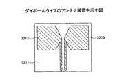
図18はダイポールタイプのアンテナ装置の構成図を示す。 FIG. 18 shows a configuration diagram of a dipole antenna device.
ダイポールタイプのアンテナ装置800は、第1のエレメントパターン811とそれを接続パッド812に接続するためのストリップライン813及び第2のエレメントパターン821とそれを接続パッド822に接続するためのストリップライン823とをフレキシブルプリント配線板831上に形成した構成とされている。 The
ダイポールタイプのアンテナ装置800でもモノポールタイプのアンテナ装置100などと同様な作用効果を奏することが可能となる。 The dipole
〔実装方法〕
次に、アンテナ装置をマウス、キーボード、携帯電話機などの電子装置に実装するときの実装方法について説明する。[Mounting method]
Next, a mounting method for mounting the antenna device on an electronic device such as a mouse, a keyboard, or a mobile phone will be described.
〔第1実装例〕
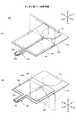
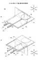
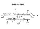
図19は第1実装例の分解斜視図、図20は第1実装例の断面図を示す。[First implementation example]
FIG. 19 is an exploded perspective view of the first mounting example, and FIG. 20 is a cross-sectional view of the first mounting example.
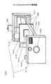
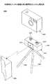
本実装例の電子機器1100は、筐体1111、1112、回路基板1113、アンテナ装置1114、同軸ケーブル1115から構成されている。 An
筐体1111、1112は、樹脂などをモールド成形した構成とされており、組み合わせることにより収納部1121が形成される。収納部1121には、回路基板1113が収納される。回路基板1113は、プリント配線板1131上に電子部品1132を搭載した構成とされている。 The
アンテナ装置1114は、前述のアンテナ装置100など同様にフレキシブルプリント配線板に導電パターンによりエレメントパターン及びグランドパターンを形成した構成とされており、薄型に構成できるため、筐体1111にインサート成形することができる。筐体1111に一体化されている。アンテナ装置1114は、筐体1111に形成された開口部1151からマイクロラインの先端が露出しており、同軸ケーブル1115により、回路基板1113に接続されている。 The
同軸ケーブル1115は、一端がアンテナ装置1114に接続され、他端が回路基板1113に接続されている。アンテナ装置1114と同軸ケーブル1115との接続は、例えば、図9、図10に示す実施例の第3変形例、図11、図12に示す第4変形例に示すように行なわれる。これによって、同軸ケーブル1115の信号線はアンテナ装置1114のエレメントパターンに接続され、同軸ケーブル1115のGND線がアンテナ装置114のGNDパターンに接続される。 The
本実装例によれば、アンテナ装置1114は筐体1111に一体に装着されるため、アンテナ装置1114を実装するためのスペースを確保する必要がなくなり、電子機器1100を小型化することが可能となる。 According to this mounting example, since the
〔第2実装例〕
図21は第1実装例の分解斜視図、図22は第2実装例の要部の断面図を示す。同図中、図19、図20と同一構成部分には同一符号を付し、その説明は省略する。[Second implementation example]
FIG. 21 is an exploded perspective view of the first mounting example, and FIG. 22 is a cross-sectional view of the main part of the second mounting example. In the figure, the same components as those in FIGS. 19 and 20 are denoted by the same reference numerals, and the description thereof is omitted.
本実装例の電子機器1200は、回路基板1113及びアンテナ装置1114と、同軸ケーブル1115とをコネクタ1211、1212により接続した構成とされている。 The
回路基板1113及びアンテナ装置1114には、ソケットコネクタ1211が搭載されている。同軸ケーブル1115の両端には、プラグコネクタ1212が取り付けられている。同軸ケーブル1115のプラグコネクタ1212を回路基板1113及びアンテナ装置1114のソケットコネクタ1211に結合することにより、回路基板1113とアンテナ装置1114とが同軸ケーブル1115を介して接続される。 A
本実装例によれば、同軸ケーブル1115と、回路基板1113及びアンテナ装置1114との接続が容易に行なえる。 According to this mounting example, the
なお、本実装例では、回路基板1113と同軸ケーブル1115との接続、及び、アンテナ装置1114と同軸ケーブル1115との接続の両方をコネクタで行なったが、いずれか一方のみをコネクタで接続するようにしてもよい。 In this mounting example, both the connection between the
なお、本実装例では、表面実装型のコネクタを使用したが、これに限定されるものではなく、例えば、エッジ実装型のコネクタなど他のコネクタであってもよく、要はケーブルが容易に接続可能なものであればよい。 In this mounting example, a surface mount type connector is used, but the present invention is not limited to this. For example, another connector such as an edge mount type connector may be used. Anything is possible.
〔第3実装例〕
図23は第3実装例の分解斜視図、図24は第3実装例の要部の断面図を示す。同図中、図21、図22と同一構成部分には同一符号を付し、その説明は省略する。[Third implementation example]
FIG. 23 is an exploded perspective view of the third mounting example, and FIG. 24 is a cross-sectional view of the main part of the third mounting example. In the figure, the same components as those in FIGS. 21 and 22 are denoted by the same reference numerals, and the description thereof is omitted.
本実装例の電子機器1300は、回路基板1113とアンテナ装置1114とをコネクタ1311、1312により直接接続する構成とされている。 The
ソケットコネクタ1311は、回路基板1113に搭載され、プラグコネクタ1312は、アンテナ装置1114に搭載されている。ソケットコネクタ1411とプラグコネクタ1412とは筐体1111と筐体1112とを組み付けたときに互いに対向する位置に取り付けられている。 The
筐体1111と筐体1112とを組み付けることにより、アンテナ装置1114のプラグコネクタ1412が回路基板1113のソケットコネクタ1311に挿入され、回路基板1113とアンテナ装置1114とが接続される。 By assembling the
本実装例によれば、回路基板1113とアンテナ装置1114とを直接的に接続できるため、ケーブルが不要となる。また、筐体1111と筐体1112とを組み付けることにより回路基板1113とアンテナ装置1114とが接続されるため、接続が容易に行なえる。 According to this mounting example, since the
〔第4実装例〕
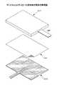
図25は第4実装例の分解斜視図、図26は第4実装例の要部の構成図を示す。同図中、図19、図20と同一構成部分には同一符号を付し、その説明は省略する。[Fourth implementation example]
FIG. 25 is an exploded perspective view of the fourth mounting example, and FIG. 26 is a configuration diagram of a main part of the fourth mounting example. In the figure, the same components as those in FIGS. 19 and 20 are denoted by the same reference numerals, and the description thereof is omitted.
本実装例の電子機器1400は、第1実装例の同軸ケーブル1115に代えてフレキシブルプリント配線板をリボン状に成形したFPCケーブル1411を介してアンテナ装置1114と回路基板1113とを接続している。FPCケーブル1411は、図26(B)に示すようにフレキシブル基板1411aの一方の面上に配線1411b、1411cを形成した構成とされている。配線1411bはアンテナ装置1114のエレメントパターンに接続され、配線1411cはアンテナ装置1114の接地パターンに接続されている。 In the
なお、このとき、FPCケーブル1411は、回路基板1113及びアンテナ装置1114に、例えば、図4乃至図8に示すようにして半田付けされる。 At this time, the
なお、本実装例では、回路基板1113とFPCケーブル1411との接続、及び、アンテナ装置1114とFPCケーブル1311とを半田付けにより行なっているが、回路基板1113及びアンテナ装置1114にコネクタを設け、コネクタにFPCケーブル1311の端部を挿入することにより、接続を図るようにしてもよい。 In this mounting example, the
〔第5実装例〕
図27は第5実装例の分解斜視図、図28は第5実装例の要部の構成図を示す。同図中、図25、図26と同一構成部分には同一符号を付し、その説明は省略する。[Fifth implementation example]
FIG. 27 is an exploded perspective view of the fifth mounting example, and FIG. 28 is a configuration diagram of a main part of the fifth mounting example. In the figure, the same components as those in FIGS. 25 and 26 are denoted by the same reference numerals, and the description thereof is omitted.
本実装例の電子機器1500は、アンテナ装置1114に一体にケーブル部1511が形成されている。ケーブル部1511は、アンテナ装置1114を構成するフレキシブルプリント配線板をケーブル状に延長した構成されている。ケーブル部1511は、信号ケーブル1511a及び接地ケーブル1511bから構成されている。信号ケーブル1511aの先端は図26(B)に示されるように回路基板1113のアンテナ接続パターン1521に半田付けされる。また、接地ケーブル1511bは図26(B)に示されるように表裏が反転するように変形した後に、回路基板1113の接地パターン1522に半田付けされる。 In the
〔第6実装例〕
図29は第6実装例の断面図、図30は第6実装例の要部の斜視図を示す。同図中、図25、図26と同一構成部分には同一符号を付し、その説明は省略する。[Sixth implementation example]
FIG. 29 is a cross-sectional view of the sixth mounting example, and FIG. 30 is a perspective view of the main part of the sixth mounting example. In the figure, the same components as those in FIGS. 25 and 26 are denoted by the same reference numerals, and the description thereof is omitted.
本実装例の電子機器1600は、FPCケーブル1411の先端と回路基板1113のアンテナ接続パターン1621及び接地パターン1622との間に異方性導電ゴム1631を介在させ、筐体1111、1112の組み付け時に、バネ1632によりFPCケーブル1411の先端を回路基板1113方向、矢印Z2方向に押圧することにより、アンテナ装置1114と回路基板1113との接続を行なっている。このとき、FPCケーブル1411は、一方の面に、矢印Z2方向側の面に配線パターン1411を有するように配置されている。
なお、異方性導電ゴム1621は、図30に示すように矢印X1、X2方向に導電体1631aと絶縁体1631bとを積層したものであり、矢印Z1、Z2方向に導電性を有し、矢印X1、X2方向には導電性を持たないように構成したものである。In the
Note that the anisotropic
筐体1111のアンテナ接続パターン1621及び接地パターン1622に対応する位置には、バネ1632が配置されている。 A
本実装例によれば、FPCケーブル1411のパターンと、回路基板1113のアンテナ接続パターン1621及び接地パターン1622とを一致させ、筐体1111と筐体1112とを組み付けることにより、FPCケーブル1411の先端部分がバネ1632により回路基板1113方向に押圧され、異方性導電ゴム1631によりFPCケーブル1611とアンテナ接続パターン1621及び接地パターン1622との接続が行なわれる。よって、接続を容易に行なえる。 According to this mounting example, the end portion of the
〔第7実装例〕
図31は第7実装例の分解斜視図、図32は第7実装例の要部の断面図を示す。同図中、図29、図30と同一構成部分には同一符号を付し、その説明は省略する。[Seventh implementation example]
FIG. 31 is an exploded perspective view of the seventh mounting example, and FIG. 32 is a cross-sectional view of the main part of the seventh mounting example. In the figure, the same components as those in FIGS. 29 and 30 are denoted by the same reference numerals, and the description thereof is omitted.
本実装例の電子機器1700は、FPCケーブル1411の先端と回路基板1113のアンテナ接続パターン1621及び接地パターン1622との間に異方性導電膜1711を介在させ、矢印Z2方向に熱圧着を行なうことにより、アンテナ装置1114と回路基板1113との接続を行なっている。なお、異方性導電膜1711は、熱硬化樹脂に導電性粒子を配合したものであり、熱圧着することにより、図32(B)に示すようにアンテナ接続パターン1621とFPCケーブル1411の配線1411bとの間に導電性粒子が介在し、かつ、接地パターン1622とFPCケーブル1411の配線1411cとの間に導電性粒子が介在することにより、圧着された方向、矢印Z1、Z2方向に導電性を持つようになる。 In the
本実装例によれば、ケーブル部1343のパターンと、回路基板1113のアンテナ接続パターン1511とを一致させ、熱圧着することによりケーブル部1343と回路基板1113との接続が可能となり、よって、接続を容易に行なえる。 According to this mounting example, the cable portion 1343 and the
〔第8実装例〕
図33は第8実装例の分解斜視図、図34は第8実装例の要部の断面図を示す。同図中、図31、図32と同一構成部分には同一符号を付し、その説明は省略する。[Eighth implementation example]
FIG. 33 is an exploded perspective view of the eighth mounting example, and FIG. 34 is a cross-sectional view of the main part of the eighth mounting example. In the figure, the same components as those in FIGS. 31 and 32 are denoted by the same reference numerals, and the description thereof is omitted.
本実装例の電子機器1800は、回路基板1113のアンテナ接続パターン1621にバネ接点部材1811を半田付けし、筐体1111、1112の組み付け時に、FPCケーブル1411の先端を筐体1111に設けられた凸部1812によりバネ接点部材1811に押し付けることにより、アンテナ装置1114と回路基板1113との接続を図っている。なお、バネ接点部材1811は、アンテナ接続パターン1621にかしめ、圧着などにより接続してもよい。 In the
本実装例によれば、筐体1111を筐体1112に組み付けることによりケーブル部1343を回路基板1113に接続が可能となり、接続を容易に行なえる。 According to this mounting example, by attaching the
〔第9実装例〕
図35は第9実装例の断面図、図36は第9実装例の要部の斜視図を示す。同図中、図29、図30と同一構成部分には同一符号を付し、その説明は省略する。[Ninth implementation example]
FIG. 35 is a cross-sectional view of the ninth mounting example, and FIG. 36 is a perspective view of the main part of the ninth mounting example. In the figure, the same components as those in FIGS. 29 and 30 are denoted by the same reference numerals, and the description thereof is omitted.
本実装例の電子機器1900は、アンテナ装置1114に一体にケーブル部1911が形成されている。ケーブル部1911は、アンテナ装置1114を構成するフレキシブルプリント配線板1114aをケーブル状に延長した構成されており、一面、矢印Z2方向側の面に、エレメントパターンに接続された配線1911aが形成されており、他面、矢印Z1方向側の面に、エレメントパターンに接続された配線1911bが形成されている。なお、アンテナ装置1114は、矢印Z1方向側の面に接地パターンが形成されており、矢印Z2方向側の面にエレメントパターン114cが形成されている。 In the
また、回路基板1113には、アンテナ接続パターン1921が形成されている。筐体1111には、アンテナ接続パターン1921に対向する位置にバネ1931が固定されている。バネ1931は、ケーブル1941などにより回路基板1113の接地パターンに接続されている。 An
バネ1931と回路基板1113のアンテナ接続パターン1921との間にケーブル部1911を挟むことにより、エレメントパターン1114cに接続された配線1911aがアンテナ接続パターン1921に接続され、接地パターン1114bに接続された配線1911bがバネ1931に接続され接地される。 By sandwiching the
〔第10実装例〕
図37は第10実装例の分解斜視図、図38は第10実装例の要部の断面図を示す。同図中、図19、図20と同一構成部分には同一符号を付し、その説明は省略する。[Tenth implementation example]
FIG. 37 is an exploded perspective view of the tenth mounting example, and FIG. 38 is a cross-sectional view of the main part of the tenth mounting example. In the figure, the same components as those in FIGS. 19 and 20 are denoted by the same reference numerals, and the description thereof is omitted.
本実施例の電子機器2000は、アンテナパターン2011を筐体1111の表面に直接に描画した構成とされている。筐体1111は、所定の誘電率の誘電体から構成されている。アンテナパターン2011は、エレメントパターン2011a及び接地パターン2011bから構成され、金属板を筐体1111の成形時にインサートモールド成形したり、筐体1111の成形後にメッキ、導電性ペーストによる印刷、スパッタリング、蒸着などによる成膜、或いは、ラミネートなどにより形成されている。 The
エレメントパターン2011aと接地パターン2011bとはアンテナ装置1114と同様な配置となるように筐体1111に形成されている。エレメントパターン2011aは筐体1111の表面側、矢印Z1方向側の面に形成されており、筐体1111の表面側と裏面側とを貫通する貫通孔2012を介して裏面側に導入されている。接地パターン1811bは、筐体1111の裏面側に形成されている。 The
また、回路基板1113には、貫通孔2012に対向する位置に接続ピン2013が植設されるとともに、接地パターン2011bに対向する位置に接続バネ2013が固着されている。接続ピン2013は、回路基板1113のアンテナ接続パターンに接続されており、筐体1111を組み付け時に貫通孔2012に挿入される。接続ピン2013は、貫通孔2012内で貫通孔2012内壁を押圧する。これによって、接続ピン2013は、エレメントパターン2011aに接続される。また、接続バネ1813は、筐体1111を筐体1112に組み付けたときに、回路基板1113の接地パターンに接続されており、筐体1111を組み付けた時に接地パターン2011bに接続される。 The
本実装例によれば、筐体1111を回路基板1113を内蔵して筐体1111に組み付けることにより、アンテナパターン2011を回路基板1113に接続することが可能となるため、接続を容易に行なえる。 According to the present mounting example, the
なお、エレメントパターン2011a及び接地パターン2011bの形状は、得ようとする特性及び筐体1111の誘電率などに基づいて決定されている。 Note that the shapes of the
また、アンテナパターン2011の成形は、インサートモールド成形、メッキに限定されるものではなく、他に、例えば、インモールド成形、ホットスタンプ成形などであってもよい。 The formation of the
インモールド成形は、アンテナパターン2011が金属蒸着などによって形成されたインモールド用フィルムを金型底面に装着した後に筐体1111をモールド成形することにより、筐体1111の表面にアンテナパターン2011を筐体1111と一体に成形する成形技術である。 In-mold molding is performed by mounting the in-mold film on which the
〔第11実装例〕
図39は第11実装例の分解斜視図、図40は第11実装例の要部の断面図を示す。同図中、図37、図38と同一構成部分には同一符号を付し、その説明は省略する。[Eleventh implementation example]
FIG. 39 is an exploded perspective view of the eleventh mounting example, and FIG. 40 is a cross-sectional view of the main part of the eleventh mounting example. In the figure, the same components as those in FIGS. 37 and 38 are denoted by the same reference numerals, and the description thereof is omitted.
本実装例の電子機器2100は、筐体1111の表面に形成されたエレメントパターン2011a上に保護膜2111が形成された構成とされている。なお、保護膜2111は、筐体1111の表面側全面に渡って形成するようにしてもよい。 The electronic device 2100 of this mounting example has a configuration in which a
エレメントパターン2011aは、貫通孔2012を通って筐体1111の裏面側に回り込んで形成されている。保護膜2111は貫通孔2012の内部にも形成されるため、本実装例では接続ピン2013に代えて接続バネ2112によりアンテナパターン2011aと接続する。接続バネ2112は回路基板1113のアンテナ接続パターンに半田付けされており、筐体1111を筐体1112に組み付けたときに、筐体1111の裏面により押圧されて弾性変形して、エレメントパターン2011aに接触する。 The
〔第12実装例〕
図41は第12実装例の分解斜視図、図42は第13実装例の要部の断面図を示す。同図中、図37、図38と同一構成部分には同一符号を付し、その説明は省略する。[Twelfth implementation example]
41 is an exploded perspective view of the twelfth mounting example, and FIG. 42 is a cross-sectional view of the main part of the thirteenth mounting example. In the figure, the same components as those in FIGS. 37 and 38 are denoted by the same reference numerals, and the description thereof is omitted.
本実施例の電子機器2200は、筐体2211が筐体本体2212及びカバー2213から構成されている。筐体本体2212とカバー2213との間には収納部2221が形成される。収納部2221には、例えば、電池パックなどが収納される。 In the electronic device 2200 of this embodiment, the
アンテナパターン2011はカバー2113に直接に描画した構成とされている。 The
エレメントパターン2011aと接地パターン2011bとはアンテナ装置1114と同様な配置となるようにカバー2113に形成されている。エレメントパターン2011aはカバー2213の表面側、矢印Z1方向側の面に形成されており、カバー2213の端面に導入されている。接地パターン1811bは、カバー2213の裏面側、矢印Z2方向側の面に形成されている。 The
また、回路基板1113には、カバー2213の端面に対向する位置に接続バネ2221が植設されるとともに、接地パターン2011bに対向する位置に接続バネ2222が植設されている。接続バネ2221は、回路基板1113のアンテナ接続パターンに接続されており、カバー2213を組み付け時に筐体本体2212とカバー2213との間に挿入される。接続バネ2221は、カバー2213の端面でエレメントパターン2011aに接触する。これによって、エレメントパターン2011aが回路基板1113に接続される。 On the
また、接続バネ2222は、カバー2213を筐体本体2212に組み付けたときに、回路基板1113の接地パターン2011bに接続される。これによって、接地パターン2011bが回路基板1113に接続される。 The
なお、第11実装例のようにエレメントパターン2011aについてもカバー2213の裏面側で接続バネによって回路基板1113に接続するようにしてもよい。さらに、第11実装例のようにエレメントパターン2011a上に保護膜を設けるようにしてもよい。 Note that the
〔その他〕
なお、上記実装例では、アンテナ装置をフレキシブルプリント配線板上に導電パターンによりエレメントパターン及びグランドパターンを形成した場合について説明したが、これに限定されるものではなく、セラミック基板やエポキシ樹脂基板などに導電パターンによりエレメントパターン及びグランドパターンを形成したアンテナ装置に対しても同様な実装方法が適用できることは言うまでもない。[Others]
In the above mounting example, the antenna device has been described with respect to the case where the element pattern and the ground pattern are formed by the conductive pattern on the flexible printed wiring board. However, the present invention is not limited to this, and the antenna device may be a ceramic substrate or an epoxy resin substrate. It goes without saying that the same mounting method can be applied to an antenna device in which an element pattern and a ground pattern are formed by a conductive pattern.
また、本実装例では、筐体1111又はカバー2213の平面部分にアンテナ装置を搭載した構成について説明しているが、アンテナ装置をフレキシブル配線基板上、あるいは、筐体1111又はカバー2213に直接印刷する場合には、図43(A)に示すように筐体1111の曲面部分にアンテナ装置1114を貼付したり、図43(B)に示すように筐体1111の曲面部分にアンテナ装置1114をインサートモールド成形したり、するようにしてもよい。また、曲面部分と平面部分とにまたがって形成するようにしてもよい。 In this mounting example, the configuration in which the antenna device is mounted on the planar portion of the
さらに、上記実装例では、誘電体の両面にパターンを形成したマイクロストリップタイプのUWBアンテナに適用した例について説明したが、図44に示すように誘電体基板3111の片面に導電パターンによりエレメントパターン3112、伝送ライン3113、接地パターン3114を形成したコプレナウェーブガイドタイプのUWBアンテナ装置、図45に示すように誘電体基板3211の片面にエレメントパターン3212、3213を形成したダイポールタイプのアンテナ装置、図46に示すような誘電体基板3311上にチップアンテナ3312とマイクロストリップライン3313、接地パターン3314を形成したアンテナ装置などにも同様に適用可能であることは言うまでもない。さらには、チップアンテナであってもよい。 Furthermore, in the above-described mounting example, an example in which the pattern is applied to a microstrip type UWB antenna in which patterns are formed on both sides of a dielectric has been described. However, as shown in FIG. 44, an
このとき、特に、図44、図45に示すようなアンテナ装置はプリント配線基板の片面に導電パターンが形成されているため、第4、第6乃至第9実装例で説明したような実装方法を容易に取ることが可能となる。図46に示すようなチップアンテナとマイクロストリップラインとから構成されたアンテナにおいても片面にのみ導電パターンを設ける構成とすれば、第4、第6乃至第9実装例で説明したような実装方法を容易に取ることが可能となる。 At this time, in particular, since the antenna device as shown in FIGS. 44 and 45 has the conductive pattern formed on one side of the printed wiring board, the mounting method described in the fourth, sixth to ninth mounting examples is used. It can be easily taken. Even in an antenna composed of a chip antenna and a microstrip line as shown in FIG. 46, if the conductive pattern is provided only on one side, the mounting method described in the fourth, sixth to ninth mounting examples is used. It can be easily taken.
さらに、上記実装例では、アンテナ装置1114を筐体1111の内部にインサートモールドしたが、図47(A)に示すように表面側あるいは図47(B)に示すように裏面側に表出するように筐体1111の成形時にインサートモールド成形してもよい。アンテナ装置1114を表面側あるいは裏面側に表出するように筐体1111の成形時にインサートモールド成形することにより、金型の表面にアンテナ装置1114を配置すればよいので、アンテナ装置1114の金型への設置が容易に行なえる。また、アンテナ装置1114を金型中央に保持するためのピンなどを金型に設ける必要がないので、筐体1111表面に不要な孔が発生することを防止できる。 Further, in the above mounting example, the
なお、第10、第11実装例では、筐体1111の表面側にエレメントパターン2011aを形成し、筐体1111の裏面側に接地パターン2011bを形成したが、筐体1111の裏面側にエレメントパターン2011aを形成し、筐体1111の表面側に接地パターン2011bを形成するようにしてもよい。 In the tenth and eleventh mounting examples, the
〔適用例〕
次に本発明のアンテナ装置の適用例を説明する。[Application example]
Next, an application example of the antenna device of the present invention will be described.
〔第1適用例〕
図48は本発明のアンテナ装置の第1適用例のシステム構成図を示す。[First application example]
FIG. 48 shows a system configuration diagram of a first application example of the antenna device of the present invention.
本適用例のシステム1200は、ディジタルカメラ1201、プリンタ1202から構成されている。 A
ディジタルカメラ1201とプリンタ1202とは、UWBなどの超広帯域帯無線通信によりデータの通信が可能な構成とされており、上記構成のUWBアンテナ装置が搭載されている。 The
〔ディジタルカメラ1201〕
図49はディジタルカメラ1201の構成図を示す。[Digital camera 1201]
FIG. 49 shows a configuration diagram of the
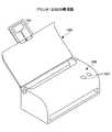
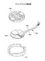
ディジタルカメラ1201は、筐体1211、フラッシュ1212、アンテナ装置1213、回路基板1214、CCD1215、光学系1216、液晶パネル1217、シャッタボタン1218、電池1219、ケーブル1220、電池カバー1221から構成とされている。 The
筐体1211は、金属などから構成されており、フロントケース1211a及びバックケース1211bから構成されている。フロントケース1211aには、フラッシュ1212及び光学系1216が取り付けられている。 The
フラッシュ1212は、ケーブル1220を介して回路基板1214に接続されており、回路基板1214からの駆動信号により発光する。また、光学系1216は、ケーブル1220を介して回路基板1214に接続されており、回路基板1214からの制御信号によりシャッタ、フォーカス、絞りなどが制御される。 The
図50はディジタルカメラ1201の要部の分解斜視図を示す。 FIG. 50 is an exploded perspective view of the main part of the
フラッシュ1212は、反射部1231、ストロボ放電管1232、レンズ部1233から構成され、筐体1211の開口部に配置されている。反射部1231は、前面が凹面状に形成されている。アンテナ装置1213は高反射率の導電材からなるアンテナ素子パターン及び接地パターンをPET、FR4などからなるフレキシブル基板に形成した構成とされており、反射部1231の前面の凹面に沿って装着される。 The
アンテナ装置1213は回路基板1214に接続されて、プリンタ1202とのデータの通信に用いられるとともに、反射鏡として作用する。 The
ストロボ放電管1232は、アンテナ装置1213の前方に取り付けられ、回路基板1214から供給される駆動信号によって、発光する。ストロボ放電管1232から出射された光は、アンテナ装置1213によって反射されて、反射部1231の開口面から出射される。反射部1231の開口面には、レンズ部1233が設けられている。 The
レンズ部1233はガラスや透明樹脂などから構成されており、ストロボ放電管1232及びアンテナ装置1213から供給された光を集光又は拡散させて、外部に出射させる。 The
本適用例によれば、アンテナ装置1213を筐体1211の金属以外の開口部であるフラッシュ1212に一体に装着することにより、アンテナ装置1213をデータの通信及びストロボ放電管1232の反射鏡として作用させることが可能となる。 According to this application example, the
なお、上記適用例では、フラッシュ1212の反射面にアンテナ装置1213を装着した構成としたが、液晶パネル1217の裏面に装着するようにしてもよい。 In the above application example, the
図51、図52はディジタルカメラ1201の変形例の要部の構成図を示す。 51 and 52 are configuration diagrams of the main part of a modification of the
本変形例では、液晶パネル1217の裏面にアンテナ装置1213が設けられる。このとき、アンテナ装置1213のアンテナ素子パターン及び接地パターンが液晶パネル1217に映り込まないようにするために、図51に示すように液晶パネル1217とアンテナ装置1213との間にフィルム1241を介在させる。フィルム1241は、遮光性を有する材料で構成されている。また、フィルム1241は、アンテナ装置1213側の面が黒色とされており、液晶パネル1217側の面が白色とされている。これによって、アンテナ装置1213のアンテナ素子パターン及び接地パターンがフィルム1231を透過することを防止でき、また、液晶パネル1217のバックライトから裏面側に漏れた光を液晶パネル1217の裏面側に戻して、バックライトの効率を向上させることができる。 In this modification, an
さらに、図52に示すようにアンテナ装置1213を黒色に着色することにより、さらに、アンテナ装置1213のアンテナ素子パターン及び接地パターンがフィルム1241の液晶パネル1217側への透過の防止をさらに強化することができる。 Furthermore, by coloring the
また、本実施例では、液晶パネル1217の裏面にアンテナ装置1213を配置するようにしたが、液晶パネル1217の表面に透明導電膜によってアンテナ素子パターン及び接地パターンを形成するようにしてもよい。 In this embodiment, the
〔プリンタ1202〕
図53はプリンタ1202の構成図、図54はプリンタ1202のブロック構成図、図55はプリンタ1202の変形例の構成図を示す。[Printer 1202]
53 is a block diagram of the
プリンタ1202は、スキャナ機能付きプリンタであり、アンテナ装置1251、通信部1252、制御部1253、プリント部1254、スキャナ部1255、インタフェース1256、操作部1257から構成されている。 The
アンテナ装置1251及び通信部1252によりディジタルカメラ1201とUWB通信が可能とされており、例えば、ディジタルカメラ1201から画像データを受信して、制御部1253によりプリント部1254を制御して、画像データのプリントを実行する。アンテナ装置1251は、例えば、プリンタ1202の原稿あるは用紙トレイ1261の上部に、図19〜図47に示すような実装方法によって実装されている。図55に示すように筐体1262の前面に図19〜図47に示すような実装方法によって実装される。 The
スキャナ部1255は原稿を読み取り、読み取った原稿の画像データを制御部1243からインタフェース1256を介してコンピュータなどに供給する。また、読み取った原稿の画像データを制御部1253から通信部1252、アンテナ装置1251を介してコンピュータなどに送信する。 The
〔第2適用例〕
図56は本発明のアンテナ装置の第2適用例のシステム構成図を示す。同図中、図48と同一構成部分には同一符号を付し、その説明は省略する。[Second application example]
FIG. 56 shows a system configuration diagram of a second application example of the antenna apparatus of the present invention. In the figure, the same components as those in FIG. 48 are denoted by the same reference numerals, and the description thereof is omitted.
本適用例のシステム1300は、ディジタルカメラ1301をクレードル1302に搭載して充電を行なうとともに、クレードル1302を介して外部機器1303とのデータ通信を行うシステムである。クレードル1302には、交流電源からACアダプタ1304を介して電源が供給されている。 A
図57はクレードル1302のブロック構成図を示す。 FIG. 57 shows a block diagram of the
クレードル1302は、図57に示すようにインタフェース部1311、通信部1312、アンテナ装置1313、電源回路1314から構成されている。 As shown in FIG. 57, the
インタフェース部1311は、コネクタ1315を介してディジタルカメラ1301と接続され、ディジタルカメラ1301と通信装置1312とのインタフェースをとる。通信装置1312は、アンテナ装置1313を介してプリンタ1202などとの通信を行う。 The
アンテナ装置1313は、クレードル1302の筐体1321に、例えば、図19〜図47に示すような実装方法によって実装されている。 The
また、電源回路1314は、ACアダプタ1303からの直流電源によりインタフェース1312、コネクタ1315を介してディジタルカメラ1301に充電を行なう。 In addition, the
〔第3適用例〕
図58は本発明のアンテナ装置の第3適用例のシステム構成図を示す。同図中、図56と同一構成部分には同一符号を付し、その説明は省略する。[Third application example]
FIG. 58 shows a system configuration diagram of a third application example of the antenna apparatus of the present invention. In the figure, the same components as those in FIG. 56 are denoted by the same reference numerals, and the description thereof is omitted.
本適用例のシステム1400は、ディジタルカメラ1301を三脚1401に搭載して三脚1401の表面に貼付されたアンテナ装置1313によりディジタルカメラ1301とプリンタ、リモコンなどの外部装置1303との通信を可能とされている。 In the
三脚1401は、台座部1421及び脚部1422から構成されている。脚部1422は、台座部1421の下部から下方の3方向に延出している。脚部1422は、例えば、伸縮可能にされている。また、台座部1421の上面からはディジタルカメラ1301を台座部1421に固定するためのねじ部1423が延出している。ねじ部1423をディジタルカメラ1301の下面に設けられたねじ孔に螺入することによりディジタルカメラ1301が台座部1421に固定される。このとき、台座部1421の上面には、コネクタ1315が設けられており、コネクタ1315は、ディジタルカメラ1301のコネクタに結合する。 The
このコネクタ1315を介してディジタルカメラ1301との通信及び電源供給を行う。 Communication with the
図59は三脚1401のブロック構成図を示す。 FIG. 59 is a block diagram of the
三脚1401の台座部1421には、インタフェース部1311、通信部1312、アンテナ装置1313、電池1411が内蔵されている。電池1411によりインタフェース部1311、通信部1312が駆動される。アンテナ装置1313は、三脚1401の台座部1421の表面に、例えば、図19〜図47に示すような実装方法によって実装されている。 An
〔第4適用例〕
図60は本発明のアンテナ装置の第4適用例のシステム構成図を示す。同図中、図53と同一構成部分には同一符号を付し、その説明は省略する。[Fourth application example]
FIG. 60 shows a system configuration diagram of a fourth application example of the antenna apparatus of the present invention. In the figure, the same components as those in FIG. 53 are denoted by the same reference numerals, and the description thereof is omitted.
本適用例のシステム1500は、ビデオカメラ1501、映像機器1502から構成されており、ビデオカメラ1501と映像機器1502とは、UWBなどの超広帯域帯無線通信によりデータの通信が可能な構成とされており、上記構成のUWBアンテナ装置が搭載されている。 The
図61はビデオカメラ1502のブロック構成図を示す。 FIG. 61 shows a block diagram of the
ビデオカメラ1501は、ビデオカメラ本体1505及びキャップ1506から構成されており、光学系1511、CCD1512、画像処理部1513、液晶パネル1514、制御部1515、記録部1516、通信部1517、アンテナ装置1518、ソケット1519、1520、インタフェース部1521、チューナ1522、操作部1523を含む構成とされている。 The
被写体の映像は光学系1511を通ってCCD1512に供給され、CCD1512で映像信号に変換される。CCD1512で変換された映像信号は画像処理部1513で画像処理されて制御部1515を通って記録部1516に供給され、記録媒体に記録される。また、通信部1517及びアンテナ装置1518、又は、インタフェース部1521を介して映像機器1502に送信される。アンテナ装置1518は、光学系1511を保護するキャップ1531に装着されている。 The image of the subject is supplied to the
図62はキャップ1531の構成図を示す。 FIG. 62 shows a configuration diagram of the
キャップ1531は、キャップ部1541及び係止部1542、ストラップ部1543から構成されている。アンテナ装置1518は、キャップ部1541の底面に貼付あるいは、例えば、図19〜図47に示すような実装方法によって実装されている。 The
係止部1542は、キャップ部1541の内側に設けられ、キャップ部1541を光学系1511に係止する。ストラップ部1543は、同軸ケーブル1551及びテレビアンテナライン1552から構成されている。 The locking
アンテナ装置1518は、同軸ケーブル1551の一端に接続されている。同軸ケーブル1551の他端には、プラグ1561が接続されている。テレビアンテナライン1552は、VHF、UHF帯の略λ/4に応じた長さの導電線から構成されており、一端には、プラグ1553が接続されている。プラグ1561、1562は、ビデオカメラ本体1510に設けられたソケット1519、ソケット1520に接続される。 The
これによって、キャップ1506がビデオカメラ本体1505に係止される。また、アンテナ装置1518が同軸ケーブル1551、ソケット1519を介して通信部1517に接続される。また、テレビアンテナライン1552がソケット1520を介してチューナ1522に接続される。テレビアンテナライン1552及びチューナ1522により受信されたテレビ放送は、制御部1515、画像処理部1513を介しては液晶パネル1514に表示される。 As a result, the
このとき、プラグ1561、1562を、ロック機構を用いてビデオカメラ本体1505にロックさせることにより、キャップ1506のビデオカメラ本体1505からの離脱を防止できる。 At this time, the
〔第5適用例〕
図63は本発明のアンテナ装置の第5適用例の構成図、図64は携帯電話1601のブロック構成図を示す。[Fifth application example]
FIG. 63 is a configuration diagram of a fifth application example of the antenna device of the present invention, and FIG. 64 is a block configuration diagram of the
本適用例は、携帯電話1601に本発明のアンテナ装置を搭載する場合の適用例を示す。 This application example shows an application example when the antenna device of the present invention is mounted on the
携帯電話1601には、UWBなどの超広帯域帯無線通信によりデータの通信が可能な構成とされており、上記構成のUWBアンテナ装置が搭載されている。 The
携帯電話1601は、携帯電話本体1611及びストラップ1612から構成されている。携帯電話本体1611は、電話部1621、カメラ部1622、電話通信部1623、制御部1624、操作部1625、UWB通信部1626、ソケット1627から構成されている。電話部1621は、マイクロフォン、スピーカ、音声処理手段などを内蔵しており、電話の機能を実現する。カメラ部1622は、CCD、画像処理手段などを内蔵しており、カメラの機能を実現している。 A
電話通信部1623は、携帯電話網との通信を行う。制御部1624は操作部1625
の操作に応じて各部の動作を制御する。UWB通信部1626は、ソケット1627に接続されるストラップ1612とともに、UWB通信を行う。The
The operation of each part is controlled in accordance with the operation. The
図63に示すようにストラップ1612は、アンテナ部1631及びストラップ部1632から構成されている。 As shown in FIG. 63, the
アンテナ部1631は、アンテナ装置1641を樹脂封止した構成とされている。アンテナ装置1641は、例えば、図4に示すような構成とされている。アンテナ装置1641はストラップ部1632に接続されている。ストラップ部1632は、同軸ケーブルから構成されており、先端には、プラグ1651が設けられている。プラグ1651は、携帯電話本体1611に設けられたソケット1627に接続される。これによって、ストラップ1612が携帯電話本体1611に係止される。また、アンテナ装置1641がUWB通信部1626に接続される。なお、プラグ1651とソケット1627との係合力は十分に大きく設定されており、ストラップ1612が携帯電話本体1611から容易に脱落することはない。 The
なお、プラグ1651のソケット1627からの脱落を防止するために、ロック機構を設けるようにしてもよい。
〔その他〕
図65、図66は特性インピーダンスを50Ωとするための基板の厚さに対するストリップライン143の線幅の関係を示す図である。
ここでは、図65(A)に示すようにεrは基板の誘電率、hは厚さ、wはストリップラインの幅を示している。このときに、図65(B)、図66に示すように基板をFR−4で構成した場合、厚さを0.01〜1mmの間で変化させたとき特性インピーダンス50Ωを得るためにはパターン幅を0.12〜1.86mmにする必要があることがわかる。また、基板をPI樹脂により構成したときには、パターン幅を0.17〜2.07mmにする必要がある。さらに、基板をPET樹脂により構成したときには、パターン幅を0.18〜2.45mmにする必要がある。
以上のように、特性インピーダンスを50Ωにするためには、基板の材質及び厚さに応じてストリップライン143の線幅を図65(B)、図66に示す関係に基づいて決定すればよい。In order to prevent the plug 1651 from dropping from the
[Others]
65 and 66 are diagrams showing the relationship of the line width of the
Here, as shown in FIG. 65A, εr represents the dielectric constant of the substrate, h represents the thickness, and w represents the width of the stripline. At this time, when the substrate is made of FR-4 as shown in FIGS. 65B and 66, in order to obtain a characteristic impedance of 50Ω when the thickness is changed between 0.01 and 1 mm, a pattern is used. It can be seen that the width needs to be 0.12 to 1.86 mm. When the substrate is made of PI resin, the pattern width needs to be 0.17 to 2.07 mm. Furthermore, when the substrate is made of PET resin, the pattern width needs to be 0.18 to 2.45 mm.
As described above, in order to set the characteristic impedance to 50Ω, the line width of the
100 アンテナ装置
111、211、311、411、511 アンテナ装置
121 フレキシブルプリント配線板、122 配線パターン
141 エレメントパターン、142 グランドパターン、143 ストリップライン
151 接続部、152、153 接続パッド
1100、1200、1300、1400、1500、1600、1700、1800、1900、2000、2100、2200 電子機器
1111、1112 筐体、1113 回路基板、1114 アンテナ装置100
Claims (5)
Translated fromJapanese前記誘電体は、可撓性を有し、高誘電率、低誘電損の材料から構成されるフィルム状の基板であり、
前記エレメントは、エレメントパターンとグランドパターンとを有するモノポールアンテナから構成され、
前記基板は、前記エレメントパターンに接続する第1の接続パターンと、前記グランドパターンに接続され、平面視で前記第1の接続パターンと同一の方向に延伸する第2の接続パターンとが形成されるとともに、平面視で前記第1の接続パターン及び前記第2の接続パターンの延伸方向に突出し、前記第1の接続パターン及び前記第2の接続パターンの先端部が形成される接続部を有し、
前記接続部は、前記第1の接続パターンの前記先端部が形成される第1接続部と、前記第1接続部と平行に延伸し、前記第2の接続パターンの前記先端部が形成される第2接続部とを含み、
前記第1の接続パターン及び前記第2の接続パターンは、前記第1接続部及び第2接続部に形成された各々の先端部を介してプリント配線板に接続されており、
前記第1の接続パターンの前記先端部と前記第2の接続パターンの前記先端部は、前記プリント配線板の互いに異なる面側で接続される、
又は、前記第1の接続パターンの前記先端部あるいは前記第2の接続パターンの前記先端部のうちのいずれか一方は、前記延伸方向においてねじられて表裏が反転されており、前記第1の接続パターンの前記先端部と前記第2の接続パターンの前記先端部は、前記プリント配線板の同一の面側で接続される、アンテナ装置。An antenna device in which an element is composed of a conductive material mounted on a dielectric,
The dielectric is a film-like substrate made of a material having flexibility, high dielectric constant, and low dielectric loss,
The element is composed of a monopole antenna having an element pattern and a ground pattern,
The substrate is formed with a first connection pattern connected to the element pattern and a second connection pattern connected to the ground pattern and extending in the same direction as the first connection pattern in plan view. together,they possess the extending direction of the first connection pattern and the second connection pattern in plan view protrudes a connection tip portion of the first connection pattern and the second connection patterns are formed,
The connection portion extends in parallel with the first connection portion where the tip portion of the first connection pattern is formed, and the tip portion of the second connection pattern is formed. A second connection part,
The first connection pattern and the second connection pattern are connected to a printed wiring board via respective tip portions formed in the first connection portion and the second connection portion,
The tip end portion of the first connection pattern and the tip end portion of the second connection pattern are connected to each other on different surface sides of the printed wiring board;
Alternatively, either the tip portion of the first connection pattern or the tip portion of the second connection pattern is twisted in the extending direction so that the front and back are reversed, and the first connection The antenna device, wherein the tip of the pattern and the tip of the second connection pattern are connected on the same surface side of the printed wiring board .
Priority Applications (9)
| Application Number | Priority Date | Filing Date | Title |
|---|---|---|---|
| JP2005328514AJP4633605B2 (en) | 2005-01-31 | 2005-11-14 | ANTENNA DEVICE AND ELECTRONIC DEVICE, ELECTRONIC CAMERA, ELECTRONIC CAMERA LIGHT EMITTING DEVICE, AND PERIPHERAL DEVICE |
| EP06250430AEP1686651A3 (en) | 2005-01-31 | 2006-01-26 | Antenna apparatus and electronic device |
| EP08153490.1AEP1944830B1 (en) | 2005-01-31 | 2006-01-26 | Antenna apparatus and electronic device |
| TW095103580ATWI332728B (en) | 2005-01-31 | 2006-01-27 | Antenna apparatus and electronic device |
| CN2006100774101ACN1862877B (en) | 2005-01-31 | 2006-01-27 | Antenna and electric device |
| US11/341,368US7339533B2 (en) | 2005-01-31 | 2006-01-30 | Antenna apparatus and electronic device |
| KR1020060009348AKR100748575B1 (en) | 2005-01-31 | 2006-01-31 | Antenna apparatus and electronic device |
| US11/972,508US7495618B2 (en) | 2005-01-31 | 2008-01-10 | Antenna apparatus and electronic device |
| US12/289,025US7986272B2 (en) | 2005-01-31 | 2008-10-17 | Antenna apparatus and electronic device |
Applications Claiming Priority (4)
| Application Number | Priority Date | Filing Date | Title |
|---|---|---|---|
| JP2005023846 | 2005-01-31 | ||
| JP2005202154 | 2005-07-11 | ||
| JP2005243040 | 2005-08-24 | ||
| JP2005328514AJP4633605B2 (en) | 2005-01-31 | 2005-11-14 | ANTENNA DEVICE AND ELECTRONIC DEVICE, ELECTRONIC CAMERA, ELECTRONIC CAMERA LIGHT EMITTING DEVICE, AND PERIPHERAL DEVICE |
Related Child Applications (1)
| Application Number | Title | Priority Date | Filing Date |
|---|---|---|---|
| JP2008114366ADivisionJP4754601B2 (en) | 2005-01-31 | 2008-04-24 | Antenna device |
Publications (3)
| Publication Number | Publication Date |
|---|---|
| JP2007089109A JP2007089109A (en) | 2007-04-05 |
| JP2007089109A5 JP2007089109A5 (en) | 2008-06-19 |
| JP4633605B2true JP4633605B2 (en) | 2011-02-16 |
Family
ID=36216901
Family Applications (1)
| Application Number | Title | Priority Date | Filing Date |
|---|---|---|---|
| JP2005328514AExpired - Fee RelatedJP4633605B2 (en) | 2005-01-31 | 2005-11-14 | ANTENNA DEVICE AND ELECTRONIC DEVICE, ELECTRONIC CAMERA, ELECTRONIC CAMERA LIGHT EMITTING DEVICE, AND PERIPHERAL DEVICE |
Country Status (6)
| Country | Link |
|---|---|
| US (3) | US7339533B2 (en) |
| EP (2) | EP1686651A3 (en) |
| JP (1) | JP4633605B2 (en) |
| KR (1) | KR100748575B1 (en) |
| CN (1) | CN1862877B (en) |
| TW (1) | TWI332728B (en) |
Families Citing this family (164)
| Publication number | Priority date | Publication date | Assignee | Title |
|---|---|---|---|---|
| KR100640365B1 (en)* | 2005-06-15 | 2006-10-30 | 삼성전자주식회사 | Antenna device of portable terminal |
| US8358816B2 (en) | 2005-10-18 | 2013-01-22 | Authentec, Inc. | Thinned finger sensor and associated methods |
| JP4762002B2 (en)* | 2006-02-27 | 2011-08-31 | 株式会社東芝 | Electronics |
| JP4811055B2 (en)* | 2006-02-28 | 2011-11-09 | ソニー株式会社 | Asymmetric planar antenna, method for manufacturing the same, and signal processing unit |
| JP2007241887A (en)* | 2006-03-10 | 2007-09-20 | Fujitsu Component Ltd | Keyboard |
| SE529319C2 (en)* | 2006-03-13 | 2007-07-03 | Amc Centurion Ab | Antenna arrangement for mobile or cellular phones, or other portable radio communication devices, includes flip provided flush with flexible film |
| TW200735458A (en)* | 2006-03-14 | 2007-09-16 | Mitac Technology Corp | Built-in antenna structure |
| JP4102411B2 (en)* | 2006-04-13 | 2008-06-18 | 株式会社東芝 | Mobile communication terminal |
| US7768461B2 (en)* | 2006-04-17 | 2010-08-03 | Getac Technology Corporation | Antenna device with insert-molded antenna pattern |
| TWI342639B (en)* | 2006-07-28 | 2011-05-21 | Lite On Technology Corp | A compact dtv receiving antenna |
| CN101114727B (en)* | 2006-07-28 | 2011-05-18 | 光宝科技股份有限公司 | A Miniaturized Digital TV Receiving Antenna |
| US7847736B2 (en)* | 2006-08-24 | 2010-12-07 | Cobham Defense Electronic Systems | Multi section meander antenna |
| DE102006057546A1 (en)* | 2006-12-06 | 2008-01-31 | Siemens Ag | Operating device for operation of machine tool, production machine or robot, has membrane keyboard with integrated antenna, which is arranged at switching foil of membrane keyboard |
| JP4764321B2 (en) | 2006-12-20 | 2011-08-31 | 株式会社東芝 | Electronics |
| JP4762126B2 (en)* | 2006-12-20 | 2011-08-31 | 株式会社東芝 | Electronics |
| KR100843442B1 (en)* | 2007-01-02 | 2008-07-03 | 삼성전기주식회사 | Film type antenna and mobile communication terminal case using the same |
| US7671817B2 (en)* | 2007-02-27 | 2010-03-02 | Sony Ericsson Mobile Communications Ab | Wideband antenna |
| CN201039143Y (en)* | 2007-04-24 | 2008-03-19 | 宁波萨基姆波导研发有限公司 | A mobile terminal RF circuit and antenna connection structure |
| JP4894610B2 (en)* | 2007-05-11 | 2012-03-14 | アイシン精機株式会社 | Terahertz wave generator and terahertz wave detector |
| JP4931689B2 (en)* | 2007-05-14 | 2012-05-16 | 株式会社秀峰 | Manufacturing method of antenna and mobile phone or personal computer provided with the antenna |
| JP4816564B2 (en)* | 2007-05-17 | 2011-11-16 | カシオ計算機株式会社 | Film antenna and electronic equipment |
| EP1995820A1 (en)* | 2007-05-25 | 2008-11-26 | Laird Technologies AB | A connector for an antenna device, an antenna device comprising such a connector and a portable radio communication device comprising such an antenna device |
| US7825862B2 (en) | 2007-06-01 | 2010-11-02 | Getac Technology Corporation | Antenna device with surface antenna pattern integrally coated casing of electronic device |
| KR20090006336A (en) | 2007-07-11 | 2009-01-15 | 삼성전기주식회사 | Case integrated antenna and manufacturing method |
| KR100826392B1 (en)* | 2007-08-08 | 2008-05-02 | 삼성전기주식회사 | Mobile device and manufacturing method thereof |
| WO2009029520A1 (en)* | 2007-08-27 | 2009-03-05 | Rambus Inc. | Antenna array with flexible interconnect for a mobile wireless device |
| JP5274801B2 (en)* | 2007-08-30 | 2013-08-28 | 京セラ株式会社 | Mobile device |
| KR101420797B1 (en)* | 2007-08-31 | 2014-08-13 | 삼성전자주식회사 | Electrical signal connecting unit and antenna apparatus and mobile communication device having the same |
| DE102008041582B4 (en)* | 2007-09-13 | 2016-02-25 | Getac Technology Corp. | Antenna device having a surface antenna pattern integrally coated on the housing of the electronic device |
| JP4756020B2 (en)* | 2007-09-25 | 2011-08-24 | 株式会社東芝 | Housing, method for manufacturing the same, and electronic device |
| JP4977902B2 (en)* | 2007-10-10 | 2012-07-18 | 国立大学法人電気通信大学 | Antenna control circuit board structure and antenna device |
| US7903033B2 (en)* | 2007-10-15 | 2011-03-08 | Symbol Technolgies, Inc. | Antennas incorporated in a fitted accessory of a mobile unit |
| JP4364271B2 (en)* | 2007-11-29 | 2009-11-11 | 株式会社東芝 | Electronics |
| JP5115253B2 (en)* | 2008-03-10 | 2013-01-09 | 富士通株式会社 | Coaxial connector mounted circuit board and method for manufacturing coaxial connector mounted circuit board |
| US20090231210A1 (en)* | 2008-03-13 | 2009-09-17 | Sony Ericsson Mobile Communications Ab | Portable device and battery |
| US8106836B2 (en)* | 2008-04-11 | 2012-01-31 | Apple Inc. | Hybrid antennas for electronic devices |
| TWI331084B (en)* | 2008-05-12 | 2010-10-01 | Asustek Comp Inc | In-mold decoration device and manufacturing method thereof |
| KR100997983B1 (en)* | 2008-05-27 | 2010-12-03 | 삼성전기주식회사 | Mobile communication terminal |
| US20100053456A1 (en)* | 2008-08-28 | 2010-03-04 | Hong Kong Applied Science And Technology Research Institute Co., Ltd. | Mobile Multimedia Terminal Antenna Systems and Methods for Use Thereof |
| CN101548429B (en)* | 2008-09-11 | 2012-12-26 | 香港应用科技研究院有限公司 | Antenna system for mobile multimedia terminal and method of use thereof |
| ITTO20080768A1 (en)* | 2008-10-21 | 2010-04-22 | Telsey S P A | MONOPOLAR PLANAR DOUBLE BAND ANTENNA |
| CN102246364B (en)* | 2008-12-16 | 2014-01-29 | 株式会社藤仓 | Cable connector and antenna component |
| CN101834343B (en)* | 2009-03-13 | 2014-03-05 | 深圳富泰宏精密工业有限公司 | Ultra-wide band antenna and wireless communication device using same |
| JP5366302B2 (en)* | 2009-04-30 | 2013-12-11 | パナソニック株式会社 | Mobile phone |
| TWI405365B (en)* | 2009-05-14 | 2013-08-11 | Wistron Corp | Electronic apparatus and antenna module thereof |
| JP5488593B2 (en)* | 2009-05-14 | 2014-05-14 | 株式会社村田製作所 | Circuit board and circuit module |
| WO2011022101A2 (en)* | 2009-05-22 | 2011-02-24 | Arizona Board Of Regents, For And On Behalf Of Arizona State University | Flexible antennas and related apparatuses and methods |
| JP5423165B2 (en)* | 2009-06-10 | 2014-02-19 | 株式会社ニコン | Imaging device |
| KR101079496B1 (en) | 2009-08-10 | 2011-11-03 | 삼성전기주식회사 | Antenna pattern frame, method and mould for manufacturing the same, electronic device having antenna pattern frame embeded therein and method for manufacturing the same |
| KR20110027572A (en)* | 2009-09-08 | 2011-03-16 | 한국전자통신연구원 | Communication device using near field |
| US20110059692A1 (en)* | 2009-09-08 | 2011-03-10 | Electronics And Telecommunications Research Institute | Communications device using near field |
| KR101090026B1 (en) | 2009-09-22 | 2011-12-05 | 삼성전기주식회사 | Antenna pattern frame, manufacturing method and manufacturing mold, manufacturing method and electronic device of electronic device case |
| TW201115823A (en)* | 2009-10-23 | 2011-05-01 | Wistron Corp | Antenna manufacturing method |
| WO2011056774A2 (en)* | 2009-11-03 | 2011-05-12 | Digi International Inc. | Compact satellite antenna |
| JP5471322B2 (en)* | 2009-11-09 | 2014-04-16 | 富士通株式会社 | Antenna device |
| JP2011160294A (en)* | 2010-02-02 | 2011-08-18 | Sony Chemical & Information Device Corp | Antenna device, and, communication device |
| US20110215975A1 (en)* | 2010-03-03 | 2011-09-08 | Digi International Inc. | Satellite antenna connection |
| KR101101468B1 (en)* | 2010-03-15 | 2012-01-03 | 삼성전기주식회사 | Electronic device case and manufacturing mold thereof, mobile communication terminal |
| KR20110117874A (en) | 2010-04-22 | 2011-10-28 | 삼성전기주식회사 | An electronic device including an antenna pattern frame, an electronics case having an antenna pattern frame, and an electronics case |
| JP5896594B2 (en)* | 2010-05-14 | 2016-03-30 | 株式会社村田製作所 | Wireless IC device |
| US8242962B2 (en)* | 2010-05-18 | 2012-08-14 | Auden Techno Corp. | Supper-broadband antenna structure |
| WO2011152538A1 (en) | 2010-06-04 | 2011-12-08 | 古河電気工業株式会社 | Printed circuit board, antenna, wireless communication device and manufacturing methods thereof |
| KR101162024B1 (en)* | 2010-06-28 | 2012-07-03 | 삼성전기주식회사 | Case having an antenna with an active module and an electronic device having the same |
| US9070969B2 (en)* | 2010-07-06 | 2015-06-30 | Apple Inc. | Tunable antenna systems |
| JP5918234B2 (en)* | 2010-08-02 | 2016-05-18 | ライフウェーブ,インコーポレーテッド | Impedance transformer pad and patient monitoring system using the same |
| KR20120013838A (en)* | 2010-08-06 | 2012-02-15 | 삼성전기주식회사 | Electronic device with antenna pattern embedded in case and manufacturing method |
| US8654031B2 (en)* | 2010-09-28 | 2014-02-18 | Raytheon Company | Plug-in antenna |
| US20120119956A1 (en)* | 2010-11-15 | 2012-05-17 | Avermedia Technologies, Inc | Antenna Device |
| JP5625829B2 (en)* | 2010-11-30 | 2014-11-19 | 三菱マテリアル株式会社 | Antenna device |
| DE102010061351A1 (en)* | 2010-12-20 | 2012-06-21 | Huf Hülsbeck & Fürst Gmbh & Co. Kg | Compact, NFC communication option having ID transmitter of a motor vehicle access system |
| US8766859B2 (en)* | 2011-01-11 | 2014-07-01 | Apple Inc. | Antenna structures with electrical connections to device housing members |
| US8791864B2 (en)* | 2011-01-11 | 2014-07-29 | Apple Inc. | Antenna structures with electrical connections to device housing members |
| US9246221B2 (en) | 2011-03-07 | 2016-01-26 | Apple Inc. | Tunable loop antennas |
| US9166279B2 (en) | 2011-03-07 | 2015-10-20 | Apple Inc. | Tunable antenna system with receiver diversity |
| US8810475B2 (en)* | 2011-03-11 | 2014-08-19 | Ibiden Co., Ltd. | Antenna device |
| US8884822B2 (en)* | 2011-05-05 | 2014-11-11 | Maxtena | Antenna system for handheld satellite communication devices |
| KR101874641B1 (en) | 2011-08-08 | 2018-07-05 | 삼성전자주식회사 | Portable terminal with wireless charging coil and antenna element in same plane |
| US9153856B2 (en)* | 2011-09-23 | 2015-10-06 | Apple Inc. | Embedded antenna structures |
| US9001002B2 (en) | 2011-09-30 | 2015-04-07 | Apple Inc. | Portable electronic device housing having insert molding around antenna |
| US9948126B2 (en) | 2011-09-30 | 2018-04-17 | Samsung Electronics Co., Ltd. | Portable terminal having wireless charging module |
| US9350069B2 (en) | 2012-01-04 | 2016-05-24 | Apple Inc. | Antenna with switchable inductor low-band tuning |
| TWI492456B (en)* | 2012-01-20 | 2015-07-11 | Univ Nat Chiao Tung | Band-notched ultrawideband antenna |
| JP6077471B2 (en)* | 2012-02-03 | 2017-02-08 | 株式会社東芝 | Antenna core, antenna and detection system using the same |
| US9190712B2 (en) | 2012-02-03 | 2015-11-17 | Apple Inc. | Tunable antenna system |
| CN102610910A (en)* | 2012-03-16 | 2012-07-25 | 浙江兆奕科技有限公司 | Built-in antenna component |
| US8836587B2 (en) | 2012-03-30 | 2014-09-16 | Apple Inc. | Antenna having flexible feed structure with components |
| JP5653384B2 (en)* | 2012-05-01 | 2015-01-14 | パナソニックモバイルコミュニケーションズ株式会社 | Retransmission device |
| US9899726B2 (en) | 2012-05-18 | 2018-02-20 | Compal Electronics, Inc. | Electronic device |
| TWI563724B (en)* | 2012-05-18 | 2016-12-21 | Compal Electronics Inc | Electronic device |
| TWM440543U (en)* | 2012-06-19 | 2012-11-01 | Askey Computer Corp | The electronic communication device with antenna structure |
| TWI487478B (en)* | 2012-07-13 | 2015-06-01 | Apone Technology Ltd | Method for forming metal member on casing |
| US9806407B2 (en)* | 2012-08-22 | 2017-10-31 | Honeywell International Inc. | Safety radio devices |
| JP6047795B2 (en)* | 2012-11-12 | 2016-12-21 | 日東電工株式会社 | Antenna module |
| KR101970861B1 (en)* | 2013-01-18 | 2019-04-19 | 미쓰비시 마테리알 가부시키가이샤 | Antenna device |
| CN103094684B (en)* | 2013-02-04 | 2016-04-20 | 上海安费诺永亿通讯电子有限公司 | A kind of water proof and dust proof antenna of FPC form |
| JP6234032B2 (en)* | 2013-02-08 | 2017-11-22 | シャープ株式会社 | Housing and wireless communication device |
| JP2014155098A (en)* | 2013-02-12 | 2014-08-25 | Nitto Denko Corp | Antenna module and method for manufacturing the same |
| JP5743034B2 (en)* | 2013-02-19 | 2015-07-01 | 株式会社村田製作所 | Inductor bridge and electronics |
| US9225058B2 (en) | 2013-03-15 | 2015-12-29 | Blackberry Limited | Flex PCB folded antenna |
| KR101301064B1 (en) | 2013-05-29 | 2013-08-28 | (주)드림텍 | Flexible antenna loaded type printed circuit board module |
| US9293815B1 (en) | 2013-09-24 | 2016-03-22 | The United States Of America As Represented By The Secretary Of The Navy | Ultra-wideband hemispherical teardrop antenna with a conical ground |
| KR101547131B1 (en)* | 2014-03-20 | 2015-08-25 | 스카이크로스 인코포레이티드 | Antenna with radiator fixed by fusion, and manufacturing method thereof |
| CN206820112U (en)* | 2014-08-12 | 2017-12-29 | 株式会社村田制作所 | antenna module |
| WO2016026999A1 (en) | 2014-08-18 | 2016-02-25 | Nokia Technologies Oy | An apparatus comprising an antenna having conductive elements |
| JP2016110075A (en) | 2014-10-03 | 2016-06-20 | 株式会社半導体エネルギー研究所 | Light-emitting device, module, and electronic device |
| US9972902B2 (en) | 2014-11-04 | 2018-05-15 | Panasonic Intellectual Property Management Co., Ltd. | Antenna device and electronic device |
| US9793599B2 (en) | 2015-03-06 | 2017-10-17 | Apple Inc. | Portable electronic device with antenna |
| CN204441445U (en)* | 2015-04-03 | 2015-07-01 | 京东方科技集团股份有限公司 | Mobile display terminal |
| DE102015208446B3 (en)* | 2015-05-06 | 2016-07-14 | Technische Universität Dresden | Transmission device with a transmitting antenna and a receiving antenna |
| US10224592B2 (en)* | 2015-07-29 | 2019-03-05 | Voxx International Corporation | Stand for planar antenna |
| KR102382041B1 (en) | 2015-11-04 | 2022-04-04 | 삼성전자주식회사 | Hot stamping wiring, electric device having the same, and method for manufacturing the same |
| CN105406179B (en)* | 2015-11-06 | 2018-08-21 | 中国电子科技集团公司第三十八研究所 | A kind of high-gain end-fire conformal antenna |
| EP3177120A1 (en)* | 2015-12-03 | 2017-06-07 | Thomson Licensing | Network device including an integrated antenna |
| US11073958B2 (en)* | 2016-01-29 | 2021-07-27 | Sharp Kabushiki Kaisha | Antenna device |
| KR101892027B1 (en)* | 2016-05-18 | 2018-08-27 | 현대자동차주식회사 | Dtg apparatus having embedded rf antenna |
| CN108521028B (en)* | 2016-07-19 | 2019-10-25 | Oppo广东移动通信有限公司 | Housing device and terminal equipment |
| CN106410394A (en)* | 2016-09-14 | 2017-02-15 | 天津大学 | Conformal dual-band monopole antenna structure |
| TWI620300B (en)* | 2017-03-16 | 2018-04-01 | 欣興電子股份有限公司 | Chip package structure and manufacturing method thereof |
| WO2018168648A1 (en)* | 2017-03-17 | 2018-09-20 | 三菱電機株式会社 | Array antenna device |
| CN113346221B (en) | 2017-03-30 | 2024-03-19 | 住友电气工业株式会社 | Wireless module |
| CN111478041A (en)* | 2017-05-24 | 2020-07-31 | 侯苏华 | Mobile communication terminal |
| CN110651395B (en) | 2017-05-30 | 2021-08-31 | 华为技术有限公司 | Multiple Antenna Systems |
| US11605883B2 (en)* | 2017-07-28 | 2023-03-14 | Samsung Electro-Mechanics Co., Ltd. | Antenna module including a flexible substrate |
| US10312590B2 (en) | 2017-07-31 | 2019-06-04 | The United States Of America As Represented By Secretary Of The Navy | Small UWB antennas and method of designing the same |
| CN107546474B (en)* | 2017-08-22 | 2020-06-05 | 南京信息职业技术学院 | Paper-based concave broadband antenna |
| US10455065B2 (en)* | 2017-09-29 | 2019-10-22 | Lg Electronics Inc. | Mobile terminal |
| KR102439813B1 (en)* | 2017-09-29 | 2022-09-02 | 엘지전자 주식회사 | mobile terminal |
| CN107834213B (en)* | 2017-11-13 | 2024-03-29 | 珠海市魅族科技有限公司 | Antenna assembly and terminal |
| TWI666821B (en)* | 2017-11-17 | 2019-07-21 | 緯創資通股份有限公司 | Antenna base for fixing an antenna body on a casing, antenna structure having the antenna base, and electronic device having the antenna structure |
| KR102387953B1 (en)* | 2017-11-28 | 2022-04-19 | 삼성전자주식회사 | An antenna and an electronic device comprising the antenna |
| US11705624B2 (en)* | 2017-11-29 | 2023-07-18 | Dai Nippon Printing Co., Ltd. | Wiring board and method for manufacturing wiring board |
| WO2019116941A1 (en)* | 2017-12-14 | 2019-06-20 | 株式会社村田製作所 | Antenna device, antenna module and wireless device |
| KR102319376B1 (en)* | 2018-01-23 | 2021-10-28 | 동우 화인켐 주식회사 | Film antenna-circuit connection structure and display device including the same |
| KR102147336B1 (en)* | 2018-01-23 | 2020-08-24 | 동우 화인켐 주식회사 | Film antenna-circuit connection structure and display device including the same |
| JP2019132684A (en)* | 2018-01-31 | 2019-08-08 | シチズン時計株式会社 | Atomic clock |
| JP7092152B2 (en) | 2018-02-05 | 2022-06-28 | 住友電気工業株式会社 | Antenna module and vehicle |
| US11411296B2 (en)* | 2018-03-07 | 2022-08-09 | The Research Foundation For The State University Of New York State | Flexible radio frequency assemblies, components thereof and related methods |
| KR102518054B1 (en)* | 2018-03-14 | 2023-04-05 | 동우 화인켐 주식회사 | Film antenna and display device including the same |
| JP7073182B2 (en)* | 2018-04-25 | 2022-05-23 | キヤノン株式会社 | Imaging device |
| KR102162228B1 (en)* | 2018-07-05 | 2020-10-06 | 동우 화인켐 주식회사 | Antenna structure and display device including the same |
| KR102494259B1 (en)* | 2018-07-23 | 2023-01-31 | 동우 화인켐 주식회사 | Antenna structure and display device including the same |
| KR102194290B1 (en)* | 2018-07-23 | 2020-12-22 | 동우 화인켐 주식회사 | Antenna structure and display device including the same |
| KR102422664B1 (en)* | 2018-10-05 | 2022-07-18 | 동우 화인켐 주식회사 | Antenna structure and display device including the same |
| KR102561724B1 (en)* | 2018-12-07 | 2023-07-31 | 삼성전자주식회사 | Antenna Module and the Electronic Device including the Antenna Module |
| KR102577769B1 (en)* | 2018-12-13 | 2023-09-13 | 엘지이노텍 주식회사 | Printed circuit board and antenna module |
| CN109728440B (en)* | 2018-12-29 | 2020-10-23 | 电子科技大学 | Planar broadband lens antenna based on transceiving structure form |
| KR102176860B1 (en)* | 2019-01-22 | 2020-11-10 | 동우 화인켐 주식회사 | Antenna structure and display device including the same |
| JP2022518481A (en) | 2019-01-22 | 2022-03-15 | 東友ファインケム株式会社 | Antenna structure and display device including it |
| US12003034B2 (en) | 2019-04-26 | 2024-06-04 | Amosense Co., Ltd | Antenna module and portable terminal cover having same |
| FI130874B1 (en)* | 2019-05-07 | 2024-05-02 | Teknologian Tutkimuskeskus Vtt Oy | Antenna element and antenna system for wireless data transmission |
| KR102785364B1 (en) | 2019-12-11 | 2025-03-20 | 동우 화인켐 주식회사 | Printed circuit board, antenna structure including the same and image display device including the same |
| WO2021201322A1 (en)* | 2020-04-02 | 2021-10-07 | 엘지전자 주식회사 | Electronic device having antenna |
| KR102781246B1 (en)* | 2020-04-28 | 2025-03-12 | 동우 화인켐 주식회사 | Antenna package and image display device including the same |
| KR102755828B1 (en)* | 2020-05-07 | 2025-01-17 | 동우 화인켐 주식회사 | Antenna package and image display device including the same |
| CN111585072B (en)* | 2020-05-29 | 2022-06-17 | 维沃移动通信有限公司 | Electronic device |
| KR102808900B1 (en)* | 2020-06-04 | 2025-05-15 | 동우 화인켐 주식회사 | Antenna package and image display device including the same |
| WO2022033683A1 (en)* | 2020-08-13 | 2022-02-17 | Huawei Technologies Co., Ltd. | Screw tower integrated coaxial connection method |
| KR102444299B1 (en)* | 2020-10-23 | 2022-09-15 | 삼성전기주식회사 | Electronic device module and manufacturing method thereof |
| CN112864610B (en)* | 2020-12-31 | 2022-09-13 | 浙江清华柔性电子技术研究院 | Flexible antenna device and method for manufacturing the same |
| EP4044363A1 (en)* | 2021-02-15 | 2022-08-17 | Koninklijke Philips N.V. | A wireless communication device |
| EP4277031A4 (en) | 2021-04-23 | 2024-06-26 | Samsung Electronics Co., Ltd. | ELECTRONIC DEVICE WITH ANTENNA MODULE |
| US12224486B2 (en)* | 2022-05-13 | 2025-02-11 | Meta Platforms Technologies, Llc | Apparatus, system, and method for swappable antenna design |
| CN115360497B (en)* | 2022-07-22 | 2024-04-05 | 青岛大学 | A flexible wearable ultra-wideband CPW antenna and preparation method thereof |
| JP2024124227A (en)* | 2023-03-02 | 2024-09-12 | メクテック株式会社 | Bonded printed wiring board, printed wiring board, and method for manufacturing bonded printed wiring board |
Family Cites Families (38)
| Publication number | Priority date | Publication date | Assignee | Title |
|---|---|---|---|---|
| JPS568902A (en)* | 1979-07-04 | 1981-01-29 | Seiko Epson Corp | Antenna unit |
| JPH02127803A (en)* | 1988-11-08 | 1990-05-16 | Kobayashi Kenji | Film antenna for sticking use |
| JPH05335826A (en)* | 1991-11-18 | 1993-12-17 | Motorola Inc | Built-in antenna for communication equipment |
| GB2292482A (en)* | 1994-08-18 | 1996-02-21 | Plessey Semiconductors Ltd | Antenna arrangement |
| BR9608629A (en) | 1995-06-02 | 1999-05-04 | Ericsson Ge Mobile Inc | Antenna |
| US7019695B2 (en)* | 1997-11-07 | 2006-03-28 | Nathan Cohen | Fractal antenna ground counterpoise, ground planes, and loading elements and microstrip patch antennas with fractal structure |
| US6476766B1 (en)* | 1997-11-07 | 2002-11-05 | Nathan Cohen | Fractal antenna ground counterpoise, ground planes, and loading elements and microstrip patch antennas with fractal structure |
| WO1999027608A1 (en)* | 1997-11-22 | 1999-06-03 | Nathan Cohen | Cylindrical conformable antenna on a planar substrate |
| JP4216951B2 (en) | 1999-05-31 | 2009-01-28 | トッパン・フォームズ株式会社 | How to make a thin antenna |
| JP2000196327A (en) | 1998-12-25 | 2000-07-14 | Harada Ind Co Ltd | Film antenna device |
| SE523293C2 (en)* | 1999-11-03 | 2004-04-06 | Ericsson Telefon Ab L M | Multiband Antenna |
| JP4350237B2 (en)* | 1999-11-08 | 2009-10-21 | 富士フイルム株式会社 | camera |
| DE10024666A1 (en)* | 2000-05-18 | 2001-11-29 | Bosch Gmbh Robert | Vehicle antenna arrangement |
| JP4423771B2 (en) | 2000-06-27 | 2010-03-03 | ソニー株式会社 | Memory module |
| AU2001296131A1 (en)* | 2000-10-13 | 2002-04-22 | Avantego Ab | Internal antenna arrangement |
| JP2002151928A (en) | 2000-11-08 | 2002-05-24 | Toshiba Corp | Antennas and electronic devices incorporating antennas |
| US6694151B2 (en)* | 2000-12-12 | 2004-02-17 | Eastman Kodak Company | Antenna apparatus for digital cameras incorporating wideband RF transceivers |
| US6973709B2 (en)* | 2001-04-19 | 2005-12-13 | Chunghwa Picture Tubes | Method of manufacturing printed-on-display antenna for wireless device |
| NZ519721A (en)* | 2001-06-25 | 2003-11-28 | Peter Joseph Vernon | Rectangular shaped planar antenna comprising square and partial square elements defined with a bifurcated central connection |
| JP3670987B2 (en) | 2001-08-13 | 2005-07-13 | インターナショナル・ビジネス・マシーンズ・コーポレーション | ANTENNA UNIT AND COMPUTER TERMINAL HAVING THE SAME |
| US6985110B2 (en) | 2001-08-31 | 2006-01-10 | Mitsubishi Denki Kabushiki Kaisha | Antenna device, wireless communication terminal, external antenna and hand-strap |
| JP2003110342A (en) | 2001-09-26 | 2003-04-11 | Hitachi Kokusai Electric Inc | Printed antenna |
| JP2003273638A (en)* | 2002-03-13 | 2003-09-26 | Sony Corp | Wide band antenna device |
| US6621458B1 (en)* | 2002-04-02 | 2003-09-16 | Xm Satellite Radio, Inc. | Combination linearly polarized and quadrifilar antenna sharing a common ground plane |
| JP2003298347A (en)* | 2002-04-05 | 2003-10-17 | Hitachi Cable Ltd | Omnidirectional array antenna |
| US6624790B1 (en)* | 2002-05-08 | 2003-09-23 | Accton Technology Corporation | Integrated dual-band printed monopole antenna |
| JP2003332827A (en)* | 2002-05-14 | 2003-11-21 | Komatsu Ltd | Antenna and movable antenna |
| WO2003103087A2 (en)* | 2002-06-04 | 2003-12-11 | Skycross, Inc. | Wideband printed monopole antenna |
| JP3645239B2 (en) | 2002-09-06 | 2005-05-11 | シャープ株式会社 | Dipole antenna, tag and moving object identification system using the same |
| US6774853B2 (en)* | 2002-11-07 | 2004-08-10 | Accton Technology Corporation | Dual-band planar monopole antenna with a U-shaped slot |
| US20040108955A1 (en) | 2002-12-10 | 2004-06-10 | Peter Sjoblom | Multiband antenna |
| KR100553268B1 (en) | 2003-03-31 | 2006-02-20 | 주식회사 에이스테크놀로지 | Antenna manufacturing method and antenna structure using macro melt molding |
| ITRE20030042A1 (en)* | 2003-04-24 | 2004-10-25 | Ask Ind Spa | "MULTIBAND PLANAR ANTENNA" |
| US7080787B2 (en)* | 2003-07-03 | 2006-07-25 | Symbol Technologies, Inc. | Insert molded antenna |
| JP2005051747A (en)* | 2003-07-14 | 2005-02-24 | Ngk Spark Plug Co Ltd | Antenna system and method for manufacturing the same |
| US7432859B2 (en)* | 2004-03-09 | 2008-10-07 | Centurion Wireless Technologies, Inc. | Multi-band omni directional antenna |
| JP2006121189A (en) | 2004-10-19 | 2006-05-11 | Hitachi Cable Ltd | Plate broadband antenna |
| TWI245454B (en)* | 2005-02-02 | 2005-12-11 | Arcadyan Technology Corp | Low sidelobes dual band and broadband flat endfire antenna |
- 2005
- 2005-11-14JPJP2005328514Apatent/JP4633605B2/ennot_activeExpired - Fee Related
- 2006
- 2006-01-26EPEP06250430Apatent/EP1686651A3/ennot_activeCeased
- 2006-01-26EPEP08153490.1Apatent/EP1944830B1/ennot_activeCeased
- 2006-01-27CNCN2006100774101Apatent/CN1862877B/ennot_activeExpired - Fee Related
- 2006-01-27TWTW095103580Apatent/TWI332728B/ennot_activeIP Right Cessation
- 2006-01-30USUS11/341,368patent/US7339533B2/ennot_activeExpired - Fee Related
- 2006-01-31KRKR1020060009348Apatent/KR100748575B1/ennot_activeExpired - Fee Related
- 2008
- 2008-01-10USUS11/972,508patent/US7495618B2/ennot_activeExpired - Fee Related
- 2008-10-17USUS12/289,025patent/US7986272B2/ennot_activeExpired - Fee Related
Also Published As
| Publication number | Publication date |
|---|---|
| CN1862877A (en) | 2006-11-15 |
| EP1686651A2 (en) | 2006-08-02 |
| US20060170597A1 (en) | 2006-08-03 |
| US20080122705A1 (en) | 2008-05-29 |
| KR20060088073A (en) | 2006-08-03 |
| CN1862877B (en) | 2012-11-28 |
| JP2007089109A (en) | 2007-04-05 |
| EP1686651A3 (en) | 2006-08-30 |
| TW200633303A (en) | 2006-09-16 |
| KR100748575B1 (en) | 2007-08-13 |
| TWI332728B (en) | 2010-11-01 |
| US7495618B2 (en) | 2009-02-24 |
| EP1944830B1 (en) | 2015-04-08 |
| US20090058733A1 (en) | 2009-03-05 |
| EP1944830A1 (en) | 2008-07-16 |
| US7986272B2 (en) | 2011-07-26 |
| US7339533B2 (en) | 2008-03-04 |
Similar Documents
| Publication | Publication Date | Title |
|---|---|---|
| JP4633605B2 (en) | ANTENNA DEVICE AND ELECTRONIC DEVICE, ELECTRONIC CAMERA, ELECTRONIC CAMERA LIGHT EMITTING DEVICE, AND PERIPHERAL DEVICE | |
| JP4754601B2 (en) | Antenna device | |
| JP4461597B2 (en) | Wireless card module | |
| US7864116B2 (en) | Mounting structure of antenna device | |
| US7068227B2 (en) | Integrated antenna assembly | |
| CN1881680B (en) | Antenna apparatus for portable terminal | |
| US8310406B2 (en) | Antenna device | |
| US8542159B2 (en) | Cable connector and antenna component | |
| TWI321862B (en) | ||
| TWI247498B (en) | Connector unit | |
| US20080246665A1 (en) | Antenna device | |
| JP2006067254A (en) | Radio communications equipment | |
| US7663568B2 (en) | Antenna apparatus | |
| EP1359675A1 (en) | Integrated antenna assembly | |
| US7692589B2 (en) | Antenna device, electronic device, and method of manufacturing antenna device | |
| CN100399625C (en) | Concealed antenna | |
| CN216563506U (en) | Electronic equipment | |
| WO2023240987A1 (en) | Antenna assembly and electronic device | |
| JP2008227941A (en) | Antenna apparatus | |
| JP2005020766A (en) | Portable radio |
Legal Events
| Date | Code | Title | Description |
|---|---|---|---|
| A521 | Request for written amendment filed | Free format text:JAPANESE INTERMEDIATE CODE: A523 Effective date:20080424 | |
| A621 | Written request for application examination | Free format text:JAPANESE INTERMEDIATE CODE: A621 Effective date:20080424 | |
| A977 | Report on retrieval | Free format text:JAPANESE INTERMEDIATE CODE: A971007 Effective date:20091029 | |
| A131 | Notification of reasons for refusal | Free format text:JAPANESE INTERMEDIATE CODE: A131 Effective date:20091201 | |
| A521 | Request for written amendment filed | Free format text:JAPANESE INTERMEDIATE CODE: A523 Effective date:20100129 | |
| A131 | Notification of reasons for refusal | Free format text:JAPANESE INTERMEDIATE CODE: A131 Effective date:20100608 | |
| A521 | Request for written amendment filed | Free format text:JAPANESE INTERMEDIATE CODE: A523 Effective date:20100804 | |
| TRDD | Decision of grant or rejection written | ||
| A01 | Written decision to grant a patent or to grant a registration (utility model) | Free format text:JAPANESE INTERMEDIATE CODE: A01 Effective date:20101116 | |
| A01 | Written decision to grant a patent or to grant a registration (utility model) | Free format text:JAPANESE INTERMEDIATE CODE: A01 | |
| A61 | First payment of annual fees (during grant procedure) | Free format text:JAPANESE INTERMEDIATE CODE: A61 Effective date:20101117 | |
| R150 | Certificate of patent or registration of utility model | Free format text:JAPANESE INTERMEDIATE CODE: R150 | |
| FPAY | Renewal fee payment (event date is renewal date of database) | Free format text:PAYMENT UNTIL: 20131126 Year of fee payment:3 | |
| R250 | Receipt of annual fees | Free format text:JAPANESE INTERMEDIATE CODE: R250 | |
| S531 | Written request for registration of change of domicile | Free format text:JAPANESE INTERMEDIATE CODE: R313531 | |
| R350 | Written notification of registration of transfer | Free format text:JAPANESE INTERMEDIATE CODE: R350 | |
| R250 | Receipt of annual fees | Free format text:JAPANESE INTERMEDIATE CODE: R250 | |
| R250 | Receipt of annual fees | Free format text:JAPANESE INTERMEDIATE CODE: R250 | |
| R250 | Receipt of annual fees | Free format text:JAPANESE INTERMEDIATE CODE: R250 | |
| LAPS | Cancellation because of no payment of annual fees |