JP4633413B2 - Imaging apparatus and signal processing method - Google Patents
Imaging apparatus and signal processing methodDownload PDFInfo
- Publication number
- JP4633413B2 JP4633413B2JP2004254350AJP2004254350AJP4633413B2JP 4633413 B2JP4633413 B2JP 4633413B2JP 2004254350 AJP2004254350 AJP 2004254350AJP 2004254350 AJP2004254350 AJP 2004254350AJP 4633413 B2JP4633413 B2JP 4633413B2
- Authority
- JP
- Japan
- Prior art keywords
- pixels
- green
- red
- blue
- pixel signal
- Prior art date
- Legal status (The legal status is an assumption and is not a legal conclusion. Google has not performed a legal analysis and makes no representation as to the accuracy of the status listed.)
- Expired - Fee Related
Links
Images


Classifications
- H—ELECTRICITY
- H04—ELECTRIC COMMUNICATION TECHNIQUE
- H04N—PICTORIAL COMMUNICATION, e.g. TELEVISION
- H04N23/00—Cameras or camera modules comprising electronic image sensors; Control thereof
- H04N23/80—Camera processing pipelines; Components thereof
- H04N23/84—Camera processing pipelines; Components thereof for processing colour signals
- H04N23/843—Demosaicing, e.g. interpolating colour pixel values
- H—ELECTRICITY
- H04—ELECTRIC COMMUNICATION TECHNIQUE
- H04N—PICTORIAL COMMUNICATION, e.g. TELEVISION
- H04N23/00—Cameras or camera modules comprising electronic image sensors; Control thereof
- H04N23/10—Cameras or camera modules comprising electronic image sensors; Control thereof for generating image signals from different wavelengths
- H04N23/12—Cameras or camera modules comprising electronic image sensors; Control thereof for generating image signals from different wavelengths with one sensor only
- H—ELECTRICITY
- H04—ELECTRIC COMMUNICATION TECHNIQUE
- H04N—PICTORIAL COMMUNICATION, e.g. TELEVISION
- H04N25/00—Circuitry of solid-state image sensors [SSIS]; Control thereof
- H04N25/10—Circuitry of solid-state image sensors [SSIS]; Control thereof for transforming different wavelengths into image signals
- H04N25/11—Arrangement of colour filter arrays [CFA]; Filter mosaics
- H04N25/13—Arrangement of colour filter arrays [CFA]; Filter mosaics characterised by the spectral characteristics of the filter elements
- H04N25/134—Arrangement of colour filter arrays [CFA]; Filter mosaics characterised by the spectral characteristics of the filter elements based on three different wavelength filter elements
- H—ELECTRICITY
- H04—ELECTRIC COMMUNICATION TECHNIQUE
- H04N—PICTORIAL COMMUNICATION, e.g. TELEVISION
- H04N2209/00—Details of colour television systems
- H04N2209/04—Picture signal generators
- H04N2209/041—Picture signal generators using solid-state devices
- H04N2209/042—Picture signal generators using solid-state devices having a single pick-up sensor
- H04N2209/045—Picture signal generators using solid-state devices having a single pick-up sensor using mosaic colour filter
- H04N2209/046—Colour interpolation to calculate the missing colour values
Landscapes
- Engineering & Computer Science (AREA)
- Multimedia (AREA)
- Signal Processing (AREA)
- Physics & Mathematics (AREA)
- Spectroscopy & Molecular Physics (AREA)
- Color Television Image Signal Generators (AREA)
- Solid State Image Pick-Up Elements (AREA)
- Transforming Light Signals Into Electric Signals (AREA)
Description
Translated fromJapanese本発明は、撮像装置及び信号処理方法に係り、特に、固体撮像素子から出力された各画素の信号を混合して所定の信号処理を行う撮像装置及び信号処理方法に関する。 The present invention relates to an imaging apparatus and a signal processing method, and more particularly, to an imaging apparatus and a signal processing method for performing predetermined signal processing by mixing signals of pixels output from a solid-state imaging device.
CCDイメージセンサから読み出された画素を混合してから転送することによって、1フレームの転送速度を上げることが行われている。しかし、画素混合方式によっては、画素の位相がずれてしまい、静止画と同様の色補間方法では偽色が発生してしまう。 The transfer speed of one frame is increased by mixing the pixels read from the CCD image sensor and then transferring them. However, depending on the pixel mixing method, the phase of the pixels is shifted, and a false color is generated in the same color interpolation method as that for a still image.
偽色防止としては、撮像素子で撮像した画像を当該撮像素子の画素数より少ない画素数で表示する場合に、間引き処理を行わない撮像装置が開示されている(例えば、特許文献1を参照。)。 As false color prevention, an image pickup apparatus that does not perform thinning processing when an image picked up by an image pickup device is displayed with a smaller number of pixels than the number of pixels of the image pickup device is disclosed (for example, see Patent Document 1). ).
特許文献1に記載された撮像装置は、撮像面に4つの異なる分光特性を持つカラーフィルタを有し、これらのカラーフィルタが水平方向に対しては2画素周期で相異なるカラーフィルタが繰り返されて配置され、垂直方向に対しては2画素周期で相異なるカラーフィルタが繰り返され、かつ、4ライン毎に1ラインを1画素分水平方向にオフセットさせるように配置されている撮像素子を備えている。 The image pickup apparatus described in
そして、上記撮像装置は、撮像素子の4Nライン(Nは1以上の整数)毎に2ライン分の画素の信号を読み出し、上記2ライン分の信号の斜め方向に隣接する2画素の信号の加算と、垂直方向に隣接する2画素の信号の加算とを交互に行う。これにより、撮像装置は、撮像素子から所定の行の画素の信号を間引いて読み出すことができると共に、この間引いて読み出された信号からカラーの映像信号を形成することができる。 Then, the imaging device reads out signals of pixels for two lines for each 4N lines (N is an integer of 1 or more) of the imaging element, and adds signals of two pixels adjacent in the diagonal direction of the signals for the two lines. And addition of signals of two pixels adjacent in the vertical direction are alternately performed. Accordingly, the imaging apparatus can thin out and read out signals of pixels in a predetermined row from the imaging device, and can form a color video signal from the signals read out by thinning out.
また、DC成分の色を欠落させること無く、且つ、高周波・高彩度の被写体画像においても新たな偽色を発生させること無く、色補間を行う信号処理装置が開示されている(例えば、特許文献2を参照。)。 Further, a signal processing device that performs color interpolation without losing the DC component color and without generating a new false color even in a high-frequency / high-saturation subject image is disclosed (for example, Patent Document 2). See).
特許文献2に記載された信号処理装置は、相関度の高い方向に色分離し第1の色差信号を算出する第1の色差信号算出手段と、第1の色差信号算出手段とは異なる所定の演算により第2の色差信号を算出する第2の色差信号算出手段と、第1及び第2の色差信号から第1及び第2の彩度値を算出する彩度検出回路と、第1及び第2の彩度値に基づいて第1及び第2の色差信号のいずれかを選択して出力するセレクタとを有する。この結果、ナイキスト周波数を有する、縦横判定を誤判定する可能性のある部分においては、縦横両方から色分離を行って得られた色差信号が出力される。 The signal processing apparatus described in
さらに、同色の画素を混合して低解像度の画像を生成する場合に偽信号や偽色の発生を抑制するデジタルカメラが開示されている(例えば、特許文献3を参照。)。特許文献3に記載されたデジタルカメラは、ハニカム配列のCCDを有し、(4k+1)、(4k+2)列目では、B色とG色の混合画素の中心位置を固定し、(4k+1)列目のR色の混合画素の中心位置を重み付け処理により所定の位置にずらす。これにより、1列単位で混合画素の位置を均等にしているので、混合画素から画像を生成した場合の偽信号や偽色の発生を抑えている。
しかしながら、特許文献1に記載された撮像装置は、撮像素子から所定の行の画素の信号を間引いて読み出しているため、解像度が低下してしまい、画質が劣化してしまう問題がある。特許文献2に記載された信号処理装置は、色差信号を生成する際に生じる偽色を抑制するものであり、画素混合による位相ずれを考慮したものではない。 However, since the image pickup apparatus described in
また、特許文献3に記載されたデジタルカメラは、各色の画素を混合した後、R色の混合画素の中心位置をずらしただけである。このため、R色とG色、B色とG色の間で、空間周波数のずれが残ったままであり、偽色が発生してしまう問題がある。 Further, the digital camera described in
本発明は、上述した課題を解決するために提案されたものであり、偽色を低減すると共に解像感を上げることができる撮像装置及び信号処理方法を提供することを目的とする。 The present invention has been proposed to solve the above-described problems, and an object of the present invention is to provide an imaging apparatus and a signal processing method capable of reducing false colors and improving resolution.
上述した課題を解決するため、本発明に係る撮像装置は、隣接行の画素が略45度斜めに互いにずれるように複数の画素を配置すると共に、偶数行では赤色及び青色の画素のみを交互に配置し奇数行では緑色の画素のみを配置し、又は、奇数行では赤色及び青色の画素のみを交互に配置し偶数行では緑色の画素のみを配置した固体撮像素子と、前記固体撮像素子から読み出された同色画素の信号を所定範囲に含まれる所定個数毎に混合して、赤色、緑色、青色について各々画素信号を生成する画素混合手段と、前記画素混合手段により生成された赤色、緑色及び青色についての画素信号の各々の画素どうしの間隔である混合間隔に対応するように、前記画素混合手段により生成された緑色の画素信号にフィルタ処理を施すフィルタと、前記画素混合手段により生成された赤色又は青色の画素信号と、前記フィルタ処理済みの緑色の画素信号と、の相関値を演算する相関値演算手段と、前記画素混合手段により生成された緑色の画素信号と、前記相関値演算手段により演算された相関値と、に基づいて、赤色又は青色の補間信号を生成する補間手段と、を備え、前記補間手段は、前記画素混合手段により生成された緑色の画素信号に基づいて緑色の補間信号を生成し、前記緑色の補間信号と前記相関値とに基づいて、前記緑色の補間信号の空間周波数と同じ空間周波数の赤色又は青色の補間信号を生成し、前記フィルタは、前記赤色又は青色の画素信号の位相に対応するように、前記緑色の画素信号にフィルタ処理を施し、前記画素混合手段は、前記固体撮像素子から、赤色及び青色の各画素のうち行方向及び列方向で隣り合う同色の画素を頂点とする各々異なる長方形に対して当該各長方形の各頂点に対応する各同色の画素から信号を読み出し、緑色の各画素のうち行方向の連続する2つの画素と列方向の連続する3つの画素で形成される各々異なる長方形に対して当該各長方形上に存在する6つの画素から信号を読み出し、読み出された同色画素の信号を混合して、赤色、緑色、青色について各々画素信号を生成する。In order to solve the above-described problem, the image pickup apparatus according to the present invention arranges a plurality of pixels so that pixels in adjacent rows are obliquely shifted from each other by approximately 45 degrees, and alternates only red and blue pixels in even rows. A solid-state image sensor in which only green pixels are arranged in odd-numbered rows, or in which only red and blue pixels are alternately arranged in odd-numbered rows and only green pixels are arranged in even-numbered rows, and read from the solid-state image sensor. A pixel mixing unit that generates a pixel signal for each of red, green, and blue by mixing a predetermined number of signals of the same color pixels that are included in a predetermined range, and red, green, and blue generated by the pixel mixing unit A filter that performs a filtering process on the green pixel signal generated by the pixel mixing means so as to correspond to a mixing interval that is an interval between the pixels of the blue pixel signal; Correlation value calculating means for calculating a correlation value between the red or blue pixel signal generated by the mixing means and the filtered green pixel signal; and the green pixel signal generated by the pixel mixing means; Interpolating means for generating a red or blue interpolated signal based on the correlation value calculated by the correlation value calculating means, wherein the interpolating means is a green pixel generated by the pixel mixing means. Generating a green interpolation signal based on the signal, generating a red or blue interpolation signal having the same spatial frequency as the spatial frequency of the green interpolation signal based on the green interpolation signal and the correlation value, The filter performs a filtering process on the green pixel signal so as to correspond to the phase of the red or blue pixel signal, and the pixel mixing unit receives red and blue from the solid-state imaging device. For each different rectangle whose vertex is the same color pixel adjacent in the row direction and column direction among the pixels, a signal is read out from the same color pixel corresponding to each vertex of the rectangle, and the row of the green pixels For each different rectangle formed by two consecutive pixels in the direction and three consecutive pixels in the column direction, signals are read from the six pixels existing on each rectangle, and the read signals of the same color pixels are read By mixing, pixel signals are generated for red, green, and blue, respectively.
また、本発明に係る信号処理方法は、隣接行の画素が略45度斜めに互いにずれるように複数の画素を配置すると共に、偶数行では赤色及び青色の画素のみを交互に配置し奇数行では緑色の画素のみを配置し、又は、奇数行では赤色及び青色の画素のみを交互に配置し偶数行では緑色の画素のみを配置した固体撮像素子から、同色画素の信号を所定範囲に含まれる所定個数毎に混合して、赤色、緑色、青色について各々画素信号を生成し、生成された赤色、緑色及び青色についての画素信号の各々の画素どうしの間隔である混合間隔に対応するように、前記緑色の画素信号にフィルタ処理を施し、生成された赤色又は青色の画素信号と、前記フィルタ処理済みの緑色の画素信号と、の相関値を演算し、生成された緑色の画素信号と演算された相関値とに基づいて、赤色又は青色の補間信号を生成する信号処理方法であって、生成された緑色の画素信号に基づいて緑色の補間信号を生成し、前記緑色の補間信号と前記相関値とに基づいて、前記緑色の補間信号の空間周波数と同じ空間周波数の赤色又は青色の補間信号を生成し、前記赤色又は青色の画素信号の位相に対応するように、前記緑色の画素信号にフィルタ処理を施し、前記画素信号の生成では、前記固体撮像素子の赤色及び青色の各画素のうち、行方向及び列方向で隣り合う同色の画素を頂点とする各々異なる長方形に対して当該各長方形の各頂点に対応する各同色の画素から信号を読み出し、前記固体撮像素子の緑色の各画素のうち、行方向の連続する2つの画素と列方向の連続する3つの画素で形成される各々異なる長方形に対して当該各長方形上に存在する6つの画素から信号を読み出し、読み出された同色画素の信号を混合して、赤色、緑色、青色について各々画素信号を生成する。In the signal processing method according to the present invention, a plurality of pixels are arranged so that pixels in adjacent rows are obliquely shifted from each other by approximately 45 degrees, and only red and blue pixels are alternately arranged in even rows, and in odd rows. Only a green pixel is arranged, or a signal of the same color pixel is included in a predetermined range from a solid-state imaging device in which only red and blue pixels are alternately arranged in an odd row and only a green pixel is arranged in an even row. The pixel signals are generated for each of red, green, and blue by mixing each number, and the pixel signals for the generated red, green, and blue are corresponding to the mixing interval that is the interval between the pixels. The green pixel signal is filtered, the correlation value between the generated red or blue pixel signal and the filtered green pixel signal is calculated, and the generated green pixel signal is calculated. Based on the related values,a signal processing method for generating a red or blue interpolation signalto generate a green interpolation signal based on the generated green pixel signal, the green interpolation signal and the correlation value And generating a red or blue interpolation signal having the same spatial frequency as the spatial frequency of the green interpolation signal, and filtering the green pixel signal so as to correspond to the phase of the red or blue pixel signal. Processing, in the generation of the pixel signal, among the red and blue pixels of the solid-state imaging device, each of the rectangles with respect to different rectangles having the same color pixels adjacent in the row direction and the column direction as vertices. A signal is read from each pixel of the same color corresponding to each vertex, and each of the green pixels of the solid-state image sensor is formed of two consecutive pixels in the row direction and three different pixels formed in the column direction. Reading signals from six pixels existing on the each rectangle with respect to the form, by mixing the signal of the same color pixels read, red, green, and generates a respective pixel signal for the blue.
固体撮像素子は、隣接行の画素が略45度斜めに互いにずれるように複数の画素を配置すると共に、偶数行では赤色及び青色の画素のみを交互に配置し奇数行では緑色の画素のみを配置し、又は、奇数行では赤色及び青色の画素のみを交互に配置し偶数行では緑色の画素のみを配置したものである。なお、偶数行と奇数行に配置する画素の色は、異なっていてもよい。In the solid-state imaging device, a plurality of pixels are arrangedso that pixels inadjacent rows are obliquely shifted from each other by approximately 45 degrees,only red and blue pixels are alternately arranged in even rows, and only green pixels are arranged in odd rows.Alternatively, only red and blue pixels are alternately arranged in odd rows, and only green pixels are arranged in even rows . Note that the colors of the pixels arranged in the even and odd rows may be different.
画素混合手段は、固体撮像素子から読み出された同色画素の信号を所定範囲に含まれる所定個数毎に混合することで、赤色、緑色、青色について各々画素信号を生成する。所定個数とは、色毎に応じて変えていてもよい。The pixel mixing unit generates pixel signals for red, green, and blue by mixing signals of the same color pixels read from the solid-state image sensor for every predetermined numberincluded in a predeterminedrange . The predetermined number may be changed according to each color.
フィルタは、赤色、緑色及び青色についての画素信号の各々の画素どうしの間隔である混合間隔に対応するように、前記画素混合手段により生成された緑色の画素信号にフィルタ処理を施す。これにより、赤色又は青色の画素信号と、フィルタ処理済みの緑色の画素信号と、の対応付けが容易になり、互いの相関がとれる状態になる。Filters,red, so as to correspond to the mixing spaceare each interval of the pixels to each other of the pixel signalsforgreen and blue, filters the green pixel signal generated by the pixel mixing means subjected. As a result, the red or blue pixel signal and the filtered green pixel signal can be easily associated with each other and can be correlated with each other.
相関値演算手段は、画素混合手段により生成された赤色又は青色の画素信号と、フィルタ処理済みの緑色の画素信号と、の相関値を演算する。相関値は、赤色又は青色の画素信号とフィルタ処理済みの緑色の画素信号との相関を表す値であるので、基準となる緑色の画素信号が存在すれば、それに対応する赤色又は青色の画素信号を求めることが可能である。 The correlation value calculation means calculates a correlation value between the red or blue pixel signal generated by the pixel mixing means and the filtered green pixel signal. Since the correlation value is a value representing the correlation between the red or blue pixel signal and the filtered green pixel signal, if there is a reference green pixel signal, the corresponding red or blue pixel signal is present. Can be obtained.
そこで、補間手段は、画素混合手段により生成された緑色の画素信号と、相関値演算手段により演算された相関値と、に基づいて、赤色又は青色の補間信号を生成する。これにより、補間処理後の緑色の画素信号と同様の空間周波数であり、かつ位相ずれのない赤色又は青色の画素信号を得ることができる。このような赤色又は青色の画素信号は、緑色の画素信号との相関を考慮して求められたものであるので、偽色を抑制することもできる。 Therefore, the interpolation unit generates a red or blue interpolation signal based on the green pixel signal generated by the pixel mixing unit and the correlation value calculated by the correlation value calculation unit. Thereby, it is possible to obtain a red or blue pixel signal having a spatial frequency similar to that of the green pixel signal after the interpolation process and having no phase shift. Since such a red or blue pixel signal is obtained in consideration of the correlation with the green pixel signal, false color can be suppressed.
したがって、本発明に係る撮像装置及び信号処理方法によれば、赤色、緑色及び青色についての画素信号の各々の画素どうしの間隔である混合間隔に対応するように、緑色の画素信号にフィルタ処理を施し、赤色又は青色の画素信号とフィルタ処理済みの緑色の画素信号との相関値を演算し、緑色の画素信号と相関値とに基づいて赤色又は青色の補間信号を生成することにより、偽色の発生を抑制し、解像感を上げることができる。Therefore, according to the imaging device and signal processing method according to the present invention, thered, so as to correspond to the mixing spaceare each interval of the pixels to each other of the pixel signalsforgreen and blue, filters the green pixel signal False color by calculating a correlation value between the red or blue pixel signal and the filtered green pixel signal and generating a red or blue interpolation signal based on the green pixel signal and the correlation value Can be suppressed and the resolution can be improved.
本発明に係る撮像装置及び信号処理方法によれば、偽色の発生を抑制し、解像感を上げることができる。According tothe imaging apparatus and the signal processing method according tothe present invention, it is possible to suppress the generation offalse colors and improve the resolution.
以下、本発明を実施するための最良の形態について、図面を参照しながら詳細に説明する。 Hereinafter, the best mode for carrying out the present invention will be described in detail with reference to the drawings.
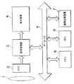
図1は、本発明の実施の形態に係る撮像装置の構成を示すブロック図である。 FIG. 1 is a block diagram showing a configuration of an imaging apparatus according to an embodiment of the present invention.
撮像装置は、撮像レンズ1を介して入射された光に応じて画像信号を生成するCCDイメージセンサ2と、CCDイメージセンサ2で生成された画像信号がディジタル信号に変換された後に所定の信号処理を実行する信号処理部3と、信号処理済みの画像信号に基づく画像を表示する表示装置4と、を備えている。 The imaging apparatus includes a
撮像装置は、さらに、信号処理部3からデータバス5を介して供給された画像信号を記憶するメモリ6と、画像信号を記録媒体に記録する画像記録装置7と、装置全体を制御する中央処理演算ユニット(CPU)8と、を備えている。 The imaging apparatus further includes a
表示装置4は、例えばLCDからなり、信号処理部3から直接供給された画像信号や、画像記録装置7に記録された画像信号に基づく画像を表示する。画像記録装置7は、例えば、フラッシュメモリ等の不揮発性半導体メモリに画像信号を記録するものでもよいし、磁気ディスクや光ディスクに画像信号を記録するものであってもよい。 The
図2は、CCDイメージセンサ2のフォトダイオードの配列を示す図である。CCDイメージセンサ2は、画素をいわゆるハニカム配列に配置したものである。 FIG. 2 is a diagram illustrating an arrangement of photodiodes of the
CCDイメージセンサ2は、八角形の形状を持つ画素(フォトダイオード)を互い違いに(正方格子を略45度回転したように)配置している。例えば、奇数行目では、R(赤)、B(青)、R、B、R、B、…の画素が交互に配置されている。偶数行目では、奇数行目の画素間の位置に、G(緑)の画素のみが配置されている。さらに再び、奇数行目ではG画素間の位置に、B、R、B、R、…の画素が交互に配置され、偶数行目では奇数行目の画素間の位置にGの画素のみが配置されている。そして、各画素から信号が読み出されて、読み出された信号は信号処理部3に供給される。 In the
以上のように構成された撮像装置において、信号処理部3は、R・G・Bに相関があることを考慮して、各画素から読み出された信号に次のような信号処理を施すことによって、RGBの各画素を補間する。 In the imaging apparatus configured as described above, the
図3は、信号処理部3による画素補間の処理手順を示すフローチャートである。すなわち、信号処理部3は、ステップS1からステップS5までの処理を実行することで、RGBの各画素を補間する。 FIG. 3 is a flowchart illustrating a pixel interpolation processing procedure performed by the
ステップS1では、信号処理部3は、CCDイメージセンサ2で生成され、ディジタル信号に変換された後の画像信号を用いて、RGBのそれぞれについて画素混合を行う。 In step S1, the
例えば、R及びBは、図2に示すように、同色の4つの画素のうち、最小の四角形を形成する画素が混合された結果、新たな1画素となる(R1、B3、R5、B7)。Gは、同色の6つの画素のうち、列方向が長手方向である長方形を形成する画素が混合された結果、新たな1画素となる(G2、G4、G6…)。なお、図2の下段には、1画素となったR1、R5、R9、B3、B7、B11、G2、G4、G6、G8、G10の混合間隔(以下、単に「間隔」という。)を示している。 For example, as shown in FIG. 2, R and B become one new pixel as a result of mixing the pixels forming the smallest square among the four pixels of the same color (R1, B3, R5, B7). . G becomes a new pixel (G2, G4, G6...) As a result of mixing pixels forming a rectangle whose column direction is the longitudinal direction among the six pixels of the same color. Note that the lower part of FIG. 2 shows a mixing interval (hereinafter simply referred to as “interval”) of R1, R5, R9, B3, B7, B11, G2, G4, G6, G8, and G10 that is one pixel. ing.
図4及び図5(A)は、ステップS1の画素混合によって得られた画素についての空間的な位相のずれを示す図である。同図に示すように、R1、B3、R5、B7は等間隔ではなく、R画素の位相がB画素の位相寄りになっている。また、R画素(B画素も同様)の間隔とG画素の間隔が異なっており、G画素はR画素よりも空間周波数成分が高くなっている。 FIG. 4 and FIG. 5 (A) are diagrams showing the spatial phase shift for the pixels obtained by the pixel mixing in step S1. As shown in the figure, R1, B3, R5, and B7 are not equally spaced, and the phase of the R pixel is closer to the phase of the B pixel. Also, the interval between the R pixels (the same applies to the B pixel) and the interval between the G pixels are different, and the G pixel has a higher spatial frequency component than the R pixel.
このように、ステップS1の処理後では、R画素に位相ずれがあり、さらにR画素(B画素も同様)とG画素との空間周波数成分の相違が存在するため、このままではRGBの相関関係(本実施形態では、RとGの相関関係、BとGの相関関係)を求めることができない。そこで、信号処理部3は、次のステップS2に移行する。 Thus, after the processing in step S1, there is a phase shift in the R pixel, and further there is a difference in the spatial frequency component between the R pixel (same for the B pixel) and the G pixel. In this embodiment, the correlation between R and G and the correlation between B and G) cannot be obtained. Therefore, the
ステップS2では、信号処理部3は、G画素にローパスフィルタ(LPF)処理を施す。これによって、R画素とG画素、B画素とG画素の相関をとれるようにして、ステップS3に移行する。例えば、R1に対応するG画素(GLPF_R1)、B3に対応するG画素(GLPF_B3)は、次のように求められる。 In step S2, the
GLPF_R1=(G0+G2*4+G4)/6
GLPF_B3=(G2+G4)/2
図6は、LPF処理後のG画素であるGLPF_R1、GLPF_B3を示す図である。図5(B)は、LPF処理後のG画素であるGLPF_R1、GLPF_B3、GLPF_R5、GLPF_B7、GLPF_R9、GLPF_B11を示す図である。これらの図に示すように、R1の間隔とGLPF_R1の間隔や、B3の間隔とGLPF_B3の間隔が一致している。また、間隔だけでなく、位相も一致している。GLPF_R1 = (G0 + G2 * 4 + G4) / 6
GLPF_B3 = (G2 + G4) / 2
FIG. 6 is a diagram illustrating GLPF_R1 and GLPF_B3 which are G pixels after the LPF processing. FIG. 5B is a diagram illustrating GLPF_R1, GLPF_B3, GLPF_R5, GLPF_B7, GLPF_R9, and GLPF_B11 that are G pixels after the LPF processing. As shown in these drawings, the interval R1 and the interval GLPF_R1, and the interval B3 and the interval GLPF_B3 are the same. Further, not only the interval but also the phase coincides.
なお、信号処理部3は、画素混合後のR画素やB画素の間隔及び位相に対応するように、G画素にLPF処理を施せばよく、上記の数式に限定されるものではない。 Note that the
ステップS3では、信号処理部3は、LPF済みのG画素とR画素及びB画素との差(相関値)を演算して、ステップS4に移行する。図5(C)は、R画素及びB画素とLPF済みのG画素との相関値を示す図である。信号処理部3は、例えば相関値R1SUB、B3SUBについては、次の演算を行う。 In step S3, the
R1SUB=R1−GLPF_R1
B3SUB=B3−GLPF_B3
R1SUBは、R1(赤)とGLPF_R1(緑)の相関値を表している。B3SUBは、B3(青)とGLPF_B3(緑)の相関値を表している。なお、図5(C)に示すように、信号処理部3は、その他、相関値R5SUB、B7SUB、R9SUB、B11SUB、…についても同様に演算する。ここでは、相関値として減算を行ったが、その他の演算を行ってもよい。R1SUB = R1-GLPF_R1
B3SUB = B3-GLPF_B3
R1SUB represents a correlation value between R1 (red) and GLPF_R1 (green). B3SUB represents a correlation value between B3 (blue) and GLPF_B3 (green). As shown in FIG. 5C, the
ステップS4では、信号処理部3は、次式のようにG画素間を補間して、ステップS5に移行する。図5(D)は、補間処理後のG画素を示す図である。 In step S4, the
G1’=(G0+G2)/2
G2’=G2
G3’=(G2+G4)/2
G4’=G4
上記式を一般化すると、次の通りになる。G1 ′ = (G0 + G2) / 2
G2 '= G2
G3 ′ = (G2 + G4) / 2
G4 '= G4
The above formula is generalized as follows.
Gn’=(G(n−1)+G(n+1))/2 (nが奇数のとき)
Gn’=Gn (nが偶数のとき)
ステップS5では、信号処理部3は、ステップS3で求めた相関値を用いてR画素及びB画素を補間する。図5(E)は補間後のR画素、(F)は補間後のB画素を示す図である。具体的には、下式に示すように、G画素に相関値を加算することで、R画素やB画素を補間する。Gn ′ = (G (n−1) + G (n + 1)) / 2 (when n is an odd number)
Gn ′ = Gn (when n is an even number)
In step S5, the
R2’=G2’+R1SUB
R3’=G3’+R1SUB
R4’=G4’+(R1SUB+R5SUB)/2
B2’=G2’+B3SUB
B3’=G3’+B3SUB
B4’=G4’+B3SUB
この結果、Rn’(nは自然数)は、ステップS4における補間処理によって求められたGn’と、ステップS3における位相ずれのないGとRの相関値と、によって生成(補間)されたものである。このため、Rn’は、図5(D)及び(E)に示すように、Gn’と同様の空間周波数及び位相を再現することができる。また、Rn’は、Gn’との相関を用いて生成されるので、偽色を抑制することできる。Bn’も同様に、図5(D)及び(F)に示すように、Gn’と同様の空間周波数及び位相を再現することができる。また、Bn’も、Gn’との相関を用いて生成されるので、偽色を抑制することできる。R2 '= G2' + R1SUB
R3 '= G3' + R1SUB
R4 '= G4' + (R1SUB + R5SUB) / 2
B2 '= G2' + B3SUB
B3 '= G3' + B3SUB
B4 '= G4' + B3SUB
As a result, Rn ′ (n is a natural number) is generated (interpolated) by Gn ′ obtained by the interpolation processing in step S4 and the correlation value of G and R without phase shift in step S3. . For this reason, as shown in FIGS. 5D and 5E, Rn ′ can reproduce the same spatial frequency and phase as Gn ′. Moreover, since Rn ′ is generated using the correlation with Gn ′, false color can be suppressed. Similarly, as shown in FIGS. 5D and 5F, Bn ′ can reproduce the same spatial frequency and phase as Gn ′. Further, since Bn ′ is also generated using the correlation with Gn ′, false color can be suppressed.
なお、R4’を演算するにあたり[(R1SUB+R5SUB)/2]を用いたのは次の通りである。R4’を演算するときに使用するG4’は、R1SUB及びR5SUBの両方と相関があるからである。 Note that [(R1SUB + R5SUB) / 2] is used in calculating R4 'as follows. This is because G4 'used when calculating R4' is correlated with both R1SUB and R5SUB.
以上のように、本発明の実施の形態に係る撮像装置は、R画素やB画素の間隔及び位相に対応するようにG画素にLPF処理を施すことによって、LPF処理後のG画素とR画素又はB画素との相関値を求めることができる。 As described above, the imaging device according to the embodiment of the present invention performs the LPF process on the G pixel so as to correspond to the interval and the phase of the R pixel and the B pixel, thereby performing the G pixel and the R pixel after the LPF process. Alternatively, the correlation value with the B pixel can be obtained.
さらに、上記撮像装置は、G画素と相関値とに基づいてR画素及びB画素を補間することにより、補間処理後のG画素と同様の空間周波数であり、かつ位相ずれのないR画素及びB画素を得ることができる。このようなR画素及びB画素は、G画素との相関を考慮して求められたものであるので、偽色を抑制することもできる。 Further, the imaging apparatus interpolates the R pixel and the B pixel based on the G pixel and the correlation value, so that the R pixel and the B have the same spatial frequency as the G pixel after the interpolation process and have no phase shift. Pixels can be obtained. Since such R pixel and B pixel are obtained in consideration of the correlation with the G pixel, false colors can be suppressed.
なお、本発明は、上述した実施の形態に限定されるものではなく、特許請求の範囲に記載された事項の範囲内で設計変更されたものについても適用可能である。例えば、LPF処理を表した数式、相関値を表した数式等は、特に限定されるものではない。また、上記撮像装置は、動画像を撮像するものでもよいし、静止画像を撮像するものでもよいのは勿論である。 In addition, this invention is not limited to embodiment mentioned above, It can apply also to what was changed in the design within the range of the matter described in the claim. For example, formulas representing LPF processing, formulas representing correlation values, and the like are not particularly limited. Of course, the imaging device may capture a moving image or may capture a still image.
1 撮像レンズ
2 CCDイメージセンサ
3 信号処理部
4 表示装置
5 データバス
6 メモリ
7 画像記録装置
8 CPUDESCRIPTION OF
Claims (6)
Translated fromJapanese前記固体撮像素子から読み出された同色画素の信号を所定範囲に含まれる所定個数毎に混合して、赤色、緑色、青色について各々画素信号を生成する画素混合手段と、
前記画素混合手段により生成された赤色、緑色及び青色についての画素信号の各々の画素どうしの間隔である混合間隔に対応するように、前記画素混合手段により生成された緑色の画素信号にフィルタ処理を施すフィルタと、
前記画素混合手段により生成された赤色又は青色の画素信号と、前記フィルタ処理済みの緑色の画素信号と、の相関値を演算する相関値演算手段と、
前記画素混合手段により生成された緑色の画素信号と、前記相関値演算手段により演算された相関値と、に基づいて、赤色又は青色の補間信号を生成する補間手段と、を備え、
前記補間手段は、前記画素混合手段により生成された緑色の画素信号に基づいて緑色の補間信号を生成し、前記緑色の補間信号と前記相関値とに基づいて、前記緑色の補間信号の空間周波数と同じ空間周波数の赤色又は青色の補間信号を生成し、
前記フィルタは、前記赤色又は青色の画素信号の位相に対応するように、前記緑色の画素信号にフィルタ処理を施し、
前記画素混合手段は、前記固体撮像素子から、赤色及び青色の各画素のうち行方向及び列方向で隣り合う同色の画素を頂点とする各々異なる長方形に対して当該各長方形の各頂点に対応する各同色の画素から信号を読み出し、緑色の各画素のうち行方向の連続する2つの画素と列方向の連続する3つの画素で形成される各々異なる長方形に対して当該各長方形上に存在する6つの画素から信号を読み出し、読み出された同色画素の信号を混合して、赤色、緑色、青色について各々画素信号を生成する撮像装置。A plurality of pixels are arranged so that pixels in adjacent rows are obliquely shifted from each other by approximately 45 degrees, and only red and blue pixels are alternately arranged in even rows, and only green pixels are arranged in odd rows, or odd numbers A solid-state imaging device in which only red and blue pixels are alternately arranged in rows and only green pixels are arranged in even rows;
Pixel mixing means for mixing signals of the same color pixels read out from the solid-state image sensor for each predetermined number included in a predetermined range, and generating pixel signals for red, green, and blue, respectively;
Filtering is performed on the green pixel signal generated by the pixel mixing unit so as to correspond to a mixing interval that is an interval between the pixels of the red, green, and blue pixel signals generated by the pixel mixing unit. Filter to apply,
Correlation value calculation means for calculating a correlation value between the red or blue pixel signal generated by the pixel mixing means and the filtered green pixel signal;
Interpolating means for generating a red or blue interpolation signal based on the green pixel signal generated by the pixel mixing means and the correlation value calculated by the correlation value calculating means,
The interpolation means generates a green interpolation signal based on the green pixel signal generated by the pixel mixing means, and based on the green interpolation signal and the correlation value, a spatial frequency of the green interpolation signal Generate a red or blue interpolation signal with the same spatial frequency as
The filter performs a filtering process on the green pixel signal so as to correspond to the phase of the red or blue pixel signal,
The pixel mixing unit corresponds to each vertex of each rectangle with respect to each different rectangle having the same color pixel adjacent in the row direction and the column direction among the red and blue pixels from the solid-state imaging device. A signal is read out from each pixel of the same color, and exists on each rectangle for each different rectangle formed by two consecutive pixels in the row direction and three consecutive pixels in the column direction among the green pixels. An imaging devicethat reads out signals from two pixels and mixes the readout signals of the same color pixels to generate pixel signals for red, green, and blue, respectively .
生成された赤色、緑色及び青色についての画素信号の各々の画素どうしの間隔である混合間隔に対応するように、前記緑色の画素信号にフィルタ処理を施し、
生成された赤色又は青色の画素信号と、前記フィルタ処理済みの緑色の画素信号と、の相関値を演算し、
生成された緑色の画素信号と演算された相関値とに基づいて、赤色又は青色の補間信号を生成する信号処理方法であって、
生成された緑色の画素信号に基づいて緑色の補間信号を生成し、前記緑色の補間信号と前記相関値とに基づいて、前記緑色の補間信号の空間周波数と同じ空間周波数の赤色又は青色の補間信号を生成し、
前記赤色又は青色の画素信号の位相に対応するように、前記緑色の画素信号にフィルタ処理を施し、
前記画素信号の生成では、前記固体撮像素子の赤色及び青色の各画素のうち、行方向及び列方向で隣り合う同色の画素を頂点とする各々異なる長方形に対して当該各長方形の各頂点に対応する各同色の画素から信号を読み出し、前記固体撮像素子の緑色の各画素のうち、行方向の連続する2つの画素と列方向の連続する3つの画素で形成される各々異なる長方形に対して当該各長方形上に存在する6つの画素から信号を読み出し、読み出された同色画素の信号を混合して、赤色、緑色、青色について各々画素信号を生成する信号処理方法。A plurality of pixels are arranged so that pixels in adjacent rows are obliquely shifted from each other by approximately 45 degrees, and only red and blue pixels are alternately arranged in even rows, and only green pixels are arranged in odd rows, or odd numbers From a solid-state imaging device in which only red and blue pixels are alternately arranged in a row and only green pixels are arranged in an even row, signals of the same color pixels are mixed every predetermined number included in a predetermined range to obtain red, green, Generate pixel signals for each blue color,
Filtering the green pixel signal so as to correspond to a mixing interval that is an interval between each pixel of the generated red, green, and blue pixel signals,
Calculating a correlation value between the generated red or blue pixel signal and the filtered green pixel signal;
A signal processing method for generating a red or blue interpolation signal based on a generated green pixel signal and a calculated correlation value,
A green interpolation signal is generated based on the generated green pixel signal, and a red or blue interpolation having the same spatial frequency as the spatial frequency of the green interpolation signal is generated based on the green interpolation signal and the correlation value. Generate a signal,
Filtering the green pixel signal to correspond to the phase of the red or blue pixel signal,
In the generation of the pixel signal, among the red and blue pixels of the solid-state imaging device, corresponding to the vertices of the respective rectangles with respect to the different rectangles having the same color pixels adjacent in the row direction and the column direction as vertices The signal is read from each pixel of the same color, and among the green pixels of the solid-state image sensor, the pixel is formed for each different rectangle formed by two consecutive pixels in the row direction and three consecutive pixels in the column direction. A signal processing method for reading out signals from six pixels present on each rectangle and mixing the read out signals of the same color pixels to generate pixel signals for red, green, and blue, respectively.
前記固体撮像素子の赤色の各画素のうち行方向及び列方向で隣り合う画素を頂点とする各々異なる長方形に対して、当該各長方形の各頂点に対応する各画素から信号を読み出し、読み出した信号を混合することで赤色画素信号を生成する赤色画素信号生成手段と、
前記固体撮像素子の青色の各画素のうち行方向及び列方向で隣り合う画素を頂点とする各々異なる長方形に対して、当該各長方形の各頂点に対応する各画素から信号を読み出し、読み出した信号を混合することで青色画素信号を生成する青色画素信号生成手段と、
前記固体撮像素子の緑色の各画素のうち行方向の連続する2つの画素と列方向の連続する3つの画素で形成される各々異なる長方形に対して、当該各長方形上に存在する6つの画素から信号を読み出し、読み出した信号を混合することで緑色画素信号を生成する緑色画素生成手段と、
前記赤色画素信号生成手段により生成された各赤色画素信号に対して、当該赤色画素信号の行方向の混合間隔と重複する行方向の混合間隔を有する複数の緑色画素信号を用いて重複の程度に応じてフィルタ処理を行うことで、赤色用緑色画素信号を生成する第1のフィルタ処理手段と、
前記青色画素信号生成手段により生成された各青色画素信号に対して、当該青色画素信号の行方向の混合間隔と重複する行方向の混合間隔を有する複数の緑色画素信号を用いて重複の程度に応じてフィルタ処理を行うことで、青色用緑色画素信号を生成する第2のフィルタ処理手段と、
前記赤色画素信号生成手段により生成された赤色画素信号と、当該赤色画素信号に対して前記第1のフィルタ手段により生成された赤色用緑画素信号と、の相関値である赤色相関値を演算し、前記青色画素信号生成手段により生成された青色画素信号と、当該青色画素信号に対して前記第2のフィルタ手段により生成された青色用緑画素信号と、の相関値である青色相関値を演算する相関値演算手段と、
前記緑色画素信号生成手段により生成された各緑色画素信号の行方向の間を補間する緑色画素信号を生成する補間緑色画素信号手段と、
前記緑色画素信号生成手段及び前記補間手段で生成された緑色画素信号のいずれか1つと、当該緑色画素信号の混合範囲に含まれる赤色相関値と、を加算することで、補間赤色画素信号を生成する補間赤色画素信号生成手段と、
前記緑色画素信号生成手段及び前記補間手段で生成された緑色画素信号のいずれか1つと、当該緑色画素信号の混合範囲に含まれる青色相関値と、を加算することで、補間青色画素信号を生成する補間青色画素信号生成手段と、
を備えた撮像装置。A plurality of pixels are arranged so that pixels in adjacent rows are obliquely shifted from each other by approximately 45 degrees, and only red and blue pixels are alternately arranged in even rows, and only green pixels are arranged in odd rows, or odd numbers A solid-state imaging device in which only red and blue pixels are alternately arranged in rows and only green pixels are arranged in even rows;
For each different rectangle whose vertex is a pixel adjacent in the row direction and the column direction among the red pixels of the solid-state imaging device, a signal is read out from each pixel corresponding to each vertex of the rectangle, and the read signal Red pixel signal generation means for generating a red pixel signal by mixing
For each different rectangle whose vertex is a pixel adjacent in the row direction and the column direction among the blue pixels of the solid-state imaging device, a signal is read from each pixel corresponding to each vertex of the rectangle, and the read signal Blue pixel signal generation means for generating a blue pixel signal by mixing
For each different rectangle formed by two consecutive pixels in the row direction and three consecutive pixels in the column direction among the green pixels of the solid-state imaging device, from the six pixels existing on the rectangles A green pixel generation means for reading a signal and generating a green pixel signal by mixing the read signals;
For each red pixel signal generated by the red pixel signal generating means, a plurality of green pixel signals having a mixing interval in the row direction that overlaps with the mixing interval in the row direction of the red pixel signal are overlapped. A first filter processing means for generating a green pixel signal for red by performing a filter process accordingly;
For each blue pixel signal generated by the blue pixel signal generating means, a plurality of green pixel signals having a mixing interval in the row direction that overlaps with the mixing interval in the row direction of the blue pixel signal are overlapped. A second filter processing means for generating a green pixel signal for blue by performing a filter process accordingly;
A red correlation value that is a correlation value between the red pixel signal generated by the red pixel signal generation unit and the red green pixel signal generated by the first filter unit with respect to the red pixel signal is calculated. A blue correlation value that is a correlation value between the blue pixel signal generated by the blue pixel signal generation unit and the blue green pixel signal generated by the second filter unit with respect to the blue pixel signal is calculated. Correlation value calculating means
Interpolating green pixel signal means for generating a green pixel signal for interpolating between the row directions of each green pixel signal generated by the green pixel signal generating means;
An interpolated red pixel signal is generated by adding any one of the green pixel signals generated by the green pixel signal generating unit and the interpolating unit and the red correlation value included in the mixed range of the green pixel signal. Interpolating red pixel signal generating means for
An interpolated blue pixel signal is generated by adding any one of the green pixel signals generated by the green pixel signal generating unit and the interpolating unit and the blue correlation value included in the mixed range of the green pixel signal. Interpolating blue pixel signal generating means for
An imaging apparatus comprising:
前記第2のフィルタ処理手段は、前記青色画素信号の行方向の混合間隔と重複する行方向の混合間隔を有する複数の緑色画素信号を用いて、重複の程度に応じた重み付け平均を計算する
請求項3に記載の撮像装置。The first filter processing means calculates a weighted average according to the degree of overlap using a plurality of green pixel signals having a mixing interval in the row direction that overlaps a mixing interval in the row direction of the red pixel signal,
The second filter processing unit calculates a weighted average according to the degree of overlap using a plurality of green pixel signals having a mixing interval in the row direction that overlaps with a mixing interval in the row direction of the blue pixel signal. Item 4. The imaging device according to Item3 .
生成された各赤色画素信号に対して、当該赤色画素信号の行方向の混合間隔と重複する行方向の混合間隔を有する複数の緑色画素信号を用いて重複の程度に応じて第1のフィルタ処理を行うことで、赤色用緑色画素信号を生成し、生成された各青色画素信号に対して、当該青色画素信号の行方向の混合間隔と重複する行方向の混合間隔を有する複数の緑色画素信号を用いて重複の程度に応じて第2のフィルタ処理を行うことで、青色用緑色画素信号を生成し、
生成された赤色画素信号と、当該赤色画素信号に対して前記フィルタ処理により生成された赤色用緑画素信号と、の相関値である赤色相関値を演算し、生成された青色画素信号と、当該青色画素信号に対して前記フィルタ処理により生成された青色用緑画素信号と、の相関値である青色相関値を演算し、
生成された各緑色画素信号の行方向の間を補間する緑色画素信号を生成し、
前記生成された又は補間された緑色画素信号のいずれか1つと、当該緑色画素信号の混合範囲に含まれる赤色相関値と、を加算することで、補間赤色画素信号を生成し、前記生成された又は補間された緑色画素信号のいずれか1つと、当該緑色画素信号の混合範囲に含まれる青色相関値と、を加算することで、補間青色画素信号を生成する信号処理方法。A plurality of pixels are arranged so that pixels in adjacent rows are obliquely shifted from each other by approximately 45 degrees, and only red and blue pixels are alternately arranged in even rows, and only green pixels are arranged in odd rows, or odd numbers From the solid-state imaging device in which only the red and blue pixels are alternately arranged in the row and only the green pixel is arranged in the even rows, each of the red pixels is a rectangle that has the adjacent pixels in the row and column directions as vertices. In contrast, a signal is read from each pixel corresponding to each vertex of each rectangle, a red pixel signal is generated by mixing the read signals, and pixels adjacent in the row direction and the column direction among the blue pixels For each of the different rectangles with vertices as the vertices, a signal is read from each pixel corresponding to each vertex of each rectangle, and a blue pixel signal is generated by mixing the read signals. For each different rectangle formed by two consecutive pixels in the direction and three consecutive pixels in the column direction, signals are read from the six pixels present on each rectangle, and the read signals are mixed together Generate a green pixel signal,
For each generated red pixel signal, a first filter process is performed according to the degree of overlap using a plurality of green pixel signals having a mixing interval in the row direction that overlaps with the mixing interval in the row direction of the red pixel signal. To generate a green pixel signal for red, and for each generated blue pixel signal, a plurality of green pixel signals having a mixing interval in the row direction that overlaps with the mixing interval in the row direction of the blue pixel signal To generate a green pixel signal for blue by performing the second filter processing according to the degree of overlap using
A red correlation value that is a correlation value between the generated red pixel signal and the green pixel signal for red generated by the filtering process on the red pixel signal is calculated, and the generated blue pixel signal Calculating a blue correlation value that is a correlation value between the blue pixel signal and the blue green pixel signal generated by the filter processing;
Generate a green pixel signal that interpolates between the row directions of each generated green pixel signal,
An interpolated red pixel signal is generated by adding any one of the generated or interpolated green pixel signals and a red correlation value included in a mixed range of the green pixel signal, and the generated Alternatively, a signal processing method for generating an interpolated blue pixel signal by adding any one of the interpolated green pixel signals and a blue correlation value included in the mixed range of the green pixel signals.
請求項5に記載の信号処理方法。In the first filter processing, a plurality of green pixel signals having a mixing interval in the row direction that overlaps with a mixing interval in the row direction of the red pixel signal is used to calculate a weighted average according to the degree of overlap, in the second filter processing, using a plurality of green pixel signals with mixed spacing in the row direction to overlap the mixing distance in the row direction of the blue pixel signal, claim to calculate the weighted average according to the degree of overlap5 A signal processing method according to claim 1.
Priority Applications (2)
| Application Number | Priority Date | Filing Date | Title |
|---|---|---|---|
| JP2004254350AJP4633413B2 (en) | 2004-09-01 | 2004-09-01 | Imaging apparatus and signal processing method |
| US11/210,678US20060044428A1 (en) | 2004-09-01 | 2005-08-25 | Image pickup device and signal processing method |
Applications Claiming Priority (1)
| Application Number | Priority Date | Filing Date | Title |
|---|---|---|---|
| JP2004254350AJP4633413B2 (en) | 2004-09-01 | 2004-09-01 | Imaging apparatus and signal processing method |
Publications (2)
| Publication Number | Publication Date |
|---|---|
| JP2006074360A JP2006074360A (en) | 2006-03-16 |
| JP4633413B2true JP4633413B2 (en) | 2011-02-16 |
Family
ID=35942496
Family Applications (1)
| Application Number | Title | Priority Date | Filing Date |
|---|---|---|---|
| JP2004254350AExpired - Fee RelatedJP4633413B2 (en) | 2004-09-01 | 2004-09-01 | Imaging apparatus and signal processing method |
Country Status (2)
| Country | Link |
|---|---|
| US (1) | US20060044428A1 (en) |
| JP (1) | JP4633413B2 (en) |
Families Citing this family (4)
| Publication number | Priority date | Publication date | Assignee | Title |
|---|---|---|---|---|
| US7511323B2 (en)* | 2005-08-11 | 2009-03-31 | Aptina Imaging Corporation | Pixel cells in a honeycomb arrangement |
| US8144984B2 (en)* | 2006-12-08 | 2012-03-27 | Canon Kabushiki Kaisha | Image processing apparatus, image processing method, and program for color fringing estimation and compensation |
| JP5068158B2 (en)* | 2007-12-28 | 2012-11-07 | イーストマン コダック カンパニー | Imaging device |
| GB2488769A (en)* | 2011-03-07 | 2012-09-12 | Sony Corp | Image Sensor Including an Array of Primary Colour Sensitive Photosensors Being Read in Line Subsets |
Family Cites Families (8)
| Publication number | Priority date | Publication date | Assignee | Title |
|---|---|---|---|---|
| US4642678A (en)* | 1984-09-10 | 1987-02-10 | Eastman Kodak Company | Signal processing method and apparatus for producing interpolated chrominance values in a sampled color image signal |
| JP2751254B2 (en)* | 1988-11-10 | 1998-05-18 | ソニー株式会社 | Signal processing circuit of solid-state imaging device |
| JP2001036809A (en)* | 1999-07-16 | 2001-02-09 | Fuji Photo Film Co Ltd | Solid-state image pickup device and image processing method |
| JP4162111B2 (en)* | 1999-07-27 | 2008-10-08 | 富士フイルム株式会社 | Image processing method and apparatus, and recording medium |
| JP4372955B2 (en)* | 2000-03-31 | 2009-11-25 | 富士フイルム株式会社 | Solid-state imaging device and signal processing method |
| JP3950655B2 (en)* | 2001-09-06 | 2007-08-01 | 富士フイルム株式会社 | Imaging device |
| JP4307780B2 (en)* | 2002-03-07 | 2009-08-05 | 富士フイルム株式会社 | Solid-state imaging device and signal reading method thereof |
| JP2003299112A (en)* | 2002-03-29 | 2003-10-17 | Fuji Photo Film Co Ltd | Digital camera |
- 2004
- 2004-09-01JPJP2004254350Apatent/JP4633413B2/ennot_activeExpired - Fee Related
- 2005
- 2005-08-25USUS11/210,678patent/US20060044428A1/ennot_activeAbandoned
Also Published As
| Publication number | Publication date |
|---|---|
| JP2006074360A (en) | 2006-03-16 |
| US20060044428A1 (en) | 2006-03-02 |
Similar Documents
| Publication | Publication Date | Title |
|---|---|---|
| JP5053654B2 (en) | Image processing apparatus and method and electronic camera | |
| CN102870417B (en) | color imaging device | |
| JP5872408B2 (en) | Color imaging apparatus and image processing method | |
| JP5702894B2 (en) | Color imaging device and imaging apparatus | |
| JP5702896B2 (en) | Color imaging device and imaging apparatus | |
| CN103444183B (en) | Color imaging element and imaging device | |
| JP4796871B2 (en) | Imaging device | |
| JP5698874B2 (en) | Color imaging device and imaging apparatus | |
| WO2012124184A1 (en) | Imaging device, method for controlling operation thereof, and imaging system | |
| WO2013099637A1 (en) | Color imaging element and imaging device | |
| JP5621057B2 (en) | Color image sensor | |
| US8786738B2 (en) | Image sensing apparatus and method of controlling operation of same | |
| JP2004336469A (en) | Solid-state imaging device, imaging apparatus, and image processing method | |
| CN101473659A (en) | Image pickup device and signal processing method | |
| JP5411390B2 (en) | Color image sensor | |
| JP4633413B2 (en) | Imaging apparatus and signal processing method | |
| JP5607267B2 (en) | IMAGING DEVICE, IMAGING DEVICE CONTROL METHOD, AND CONTROL PROGRAM | |
| JP2009033737A (en) | Signal processing device, imaging device, and synchronization processing program | |
| JP5090388B2 (en) | Imaging device | |
| JP4059837B2 (en) | Still image color camera device | |
| JP2018195961A (en) | Image signal processing method, image signal processing device, and imaging device | |
| JP2010212969A (en) | Color image sensor |
Legal Events
| Date | Code | Title | Description |
|---|---|---|---|
| A621 | Written request for application examination | Free format text:JAPANESE INTERMEDIATE CODE: A621 Effective date:20070201 | |
| A711 | Notification of change in applicant | Free format text:JAPANESE INTERMEDIATE CODE: A712 Effective date:20070201 | |
| A977 | Report on retrieval | Free format text:JAPANESE INTERMEDIATE CODE: A971007 Effective date:20090708 | |
| A131 | Notification of reasons for refusal | Free format text:JAPANESE INTERMEDIATE CODE: A131 Effective date:20090811 | |
| A521 | Request for written amendment filed | Free format text:JAPANESE INTERMEDIATE CODE: A523 Effective date:20091001 | |
| A02 | Decision of refusal | Free format text:JAPANESE INTERMEDIATE CODE: A02 Effective date:20100406 | |
| A521 | Request for written amendment filed | Free format text:JAPANESE INTERMEDIATE CODE: A523 Effective date:20100427 | |
| A911 | Transfer to examiner for re-examination before appeal (zenchi) | Free format text:JAPANESE INTERMEDIATE CODE: A911 Effective date:20100714 | |
| TRDD | Decision of grant or rejection written | ||
| A01 | Written decision to grant a patent or to grant a registration (utility model) | Free format text:JAPANESE INTERMEDIATE CODE: A01 Effective date:20101026 | |
| A01 | Written decision to grant a patent or to grant a registration (utility model) | Free format text:JAPANESE INTERMEDIATE CODE: A01 | |
| A61 | First payment of annual fees (during grant procedure) | Free format text:JAPANESE INTERMEDIATE CODE: A61 Effective date:20101117 | |
| R150 | Certificate of patent or registration of utility model | Free format text:JAPANESE INTERMEDIATE CODE: R150 | |
| FPAY | Renewal fee payment (event date is renewal date of database) | Free format text:PAYMENT UNTIL: 20131126 Year of fee payment:3 | |
| R250 | Receipt of annual fees | Free format text:JAPANESE INTERMEDIATE CODE: R250 | |
| LAPS | Cancellation because of no payment of annual fees |