JP4623955B2 - Micro-molded silicon carbide nanoimprint stamp - Google Patents
Micro-molded silicon carbide nanoimprint stampDownload PDFInfo
- Publication number
- JP4623955B2 JP4623955B2JP2003364007AJP2003364007AJP4623955B2JP 4623955 B2JP4623955 B2JP 4623955B2JP 2003364007 AJP2003364007 AJP 2003364007AJP 2003364007 AJP2003364007 AJP 2003364007AJP 4623955 B2JP4623955 B2JP 4623955B2
- Authority
- JP
- Japan
- Prior art keywords
- layer
- mold
- substrate
- etching
- silicon carbide
- Prior art date
- Legal status (The legal status is an assumption and is not a legal conclusion. Google has not performed a legal analysis and makes no representation as to the accuracy of the status listed.)
- Expired - Fee Related
Links
Images


Classifications
- B—PERFORMING OPERATIONS; TRANSPORTING
- B81—MICROSTRUCTURAL TECHNOLOGY
- B81C—PROCESSES OR APPARATUS SPECIALLY ADAPTED FOR THE MANUFACTURE OR TREATMENT OF MICROSTRUCTURAL DEVICES OR SYSTEMS
- B81C99/00—Subject matter not provided for in other groups of this subclass
- B81C99/0075—Manufacture of substrate-free structures
- B81C99/009—Manufacturing the stamps or the moulds
- B—PERFORMING OPERATIONS; TRANSPORTING
- B82—NANOTECHNOLOGY
- B82Y—SPECIFIC USES OR APPLICATIONS OF NANOSTRUCTURES; MEASUREMENT OR ANALYSIS OF NANOSTRUCTURES; MANUFACTURE OR TREATMENT OF NANOSTRUCTURES
- B82Y10/00—Nanotechnology for information processing, storage or transmission, e.g. quantum computing or single electron logic
- B—PERFORMING OPERATIONS; TRANSPORTING
- B82—NANOTECHNOLOGY
- B82Y—SPECIFIC USES OR APPLICATIONS OF NANOSTRUCTURES; MEASUREMENT OR ANALYSIS OF NANOSTRUCTURES; MANUFACTURE OR TREATMENT OF NANOSTRUCTURES
- B82Y40/00—Manufacture or treatment of nanostructures
- G—PHYSICS
- G03—PHOTOGRAPHY; CINEMATOGRAPHY; ANALOGOUS TECHNIQUES USING WAVES OTHER THAN OPTICAL WAVES; ELECTROGRAPHY; HOLOGRAPHY
- G03F—PHOTOMECHANICAL PRODUCTION OF TEXTURED OR PATTERNED SURFACES, e.g. FOR PRINTING, FOR PROCESSING OF SEMICONDUCTOR DEVICES; MATERIALS THEREFOR; ORIGINALS THEREFOR; APPARATUS SPECIALLY ADAPTED THEREFOR
- G03F7/00—Photomechanical, e.g. photolithographic, production of textured or patterned surfaces, e.g. printing surfaces; Materials therefor, e.g. comprising photoresists; Apparatus specially adapted therefor
- G03F7/0002—Lithographic processes using patterning methods other than those involving the exposure to radiation, e.g. by stamping
- B—PERFORMING OPERATIONS; TRANSPORTING
- B29—WORKING OF PLASTICS; WORKING OF SUBSTANCES IN A PLASTIC STATE IN GENERAL
- B29C—SHAPING OR JOINING OF PLASTICS; SHAPING OF MATERIAL IN A PLASTIC STATE, NOT OTHERWISE PROVIDED FOR; AFTER-TREATMENT OF THE SHAPED PRODUCTS, e.g. REPAIRING
- B29C59/00—Surface shaping of articles, e.g. embossing; Apparatus therefor
- B29C59/02—Surface shaping of articles, e.g. embossing; Apparatus therefor by mechanical means, e.g. pressing
- B29C59/022—Surface shaping of articles, e.g. embossing; Apparatus therefor by mechanical means, e.g. pressing characterised by the disposition or the configuration, e.g. dimensions, of the embossments or the shaping tools therefor
- B29C2059/023—Microembossing
- H—ELECTRICITY
- H05—ELECTRIC TECHNIQUES NOT OTHERWISE PROVIDED FOR
- H05K—PRINTED CIRCUITS; CASINGS OR CONSTRUCTIONAL DETAILS OF ELECTRIC APPARATUS; MANUFACTURE OF ASSEMBLAGES OF ELECTRICAL COMPONENTS
- H05K3/00—Apparatus or processes for manufacturing printed circuits
- H05K3/10—Apparatus or processes for manufacturing printed circuits in which conductive material is applied to the insulating support in such a manner as to form the desired conductive pattern
- H05K3/12—Apparatus or processes for manufacturing printed circuits in which conductive material is applied to the insulating support in such a manner as to form the desired conductive pattern using thick film techniques, e.g. printing techniques to apply the conductive material or similar techniques for applying conductive paste or ink patterns
- Y—GENERAL TAGGING OF NEW TECHNOLOGICAL DEVELOPMENTS; GENERAL TAGGING OF CROSS-SECTIONAL TECHNOLOGIES SPANNING OVER SEVERAL SECTIONS OF THE IPC; TECHNICAL SUBJECTS COVERED BY FORMER USPC CROSS-REFERENCE ART COLLECTIONS [XRACs] AND DIGESTS
- Y10—TECHNICAL SUBJECTS COVERED BY FORMER USPC
- Y10S—TECHNICAL SUBJECTS COVERED BY FORMER USPC CROSS-REFERENCE ART COLLECTIONS [XRACs] AND DIGESTS
- Y10S977/00—Nanotechnology
- Y10S977/84—Manufacture, treatment, or detection of nanostructure
- Y10S977/887—Nanoimprint lithography, i.e. nanostamp
- Y—GENERAL TAGGING OF NEW TECHNOLOGICAL DEVELOPMENTS; GENERAL TAGGING OF CROSS-SECTIONAL TECHNOLOGIES SPANNING OVER SEVERAL SECTIONS OF THE IPC; TECHNICAL SUBJECTS COVERED BY FORMER USPC CROSS-REFERENCE ART COLLECTIONS [XRACs] AND DIGESTS
- Y10—TECHNICAL SUBJECTS COVERED BY FORMER USPC
- Y10T—TECHNICAL SUBJECTS COVERED BY FORMER US CLASSIFICATION
- Y10T428/00—Stock material or miscellaneous articles
- Y10T428/24—Structurally defined web or sheet [e.g., overall dimension, etc.]
- Y10T428/24479—Structurally defined web or sheet [e.g., overall dimension, etc.] including variation in thickness
Landscapes
- Engineering & Computer Science (AREA)
- Chemical & Material Sciences (AREA)
- Nanotechnology (AREA)
- Physics & Mathematics (AREA)
- General Physics & Mathematics (AREA)
- Manufacturing & Machinery (AREA)
- Crystallography & Structural Chemistry (AREA)
- Microelectronics & Electronic Packaging (AREA)
- Theoretical Computer Science (AREA)
- Mathematical Physics (AREA)
- Condensed Matter Physics & Semiconductors (AREA)
- Exposure Of Semiconductors, Excluding Electron Or Ion Beam Exposure (AREA)
- Micromachines (AREA)
- Shaping Of Tube Ends By Bending Or Straightening (AREA)
- Moulds For Moulding Plastics Or The Like (AREA)
- Ceramic Products (AREA)
- Crystals, And After-Treatments Of Crystals (AREA)
- Carbon And Carbon Compounds (AREA)
Description
Translated fromJapanese本発明は、概して、炭化ケイ素から硬化ナノインプリントスタンプを形成する方法およびその構造に関する。詳しくは、本発明は、マイクロキャスティング法を用いて硬化ナノインプリントスタンプを形成する方法およびその構造に関する。 The present invention relates generally to a method and structure for forming a cured nanoimprint stamp from silicon carbide. Specifically, the present invention relates to a method for forming a cured nanoimprint stamp using a microcasting method and a structure thereof.
ナノインプリンティングリソグラフィは、極小パターン(数十ナノメートル程度)を得るための将来性のある技術である。極小パターンを形成する際の重要なステップは、スタンプで転写したい極小パターンに対して相補形状を成すパターンを有するインプリントスタンプをまず形成することである。 Nanoimprinting lithography is a promising technique for obtaining extremely small patterns (about several tens of nanometers). An important step in forming a minimal pattern is to first form an imprint stamp having a pattern that is complementary to the minimal pattern to be transferred with the stamp.
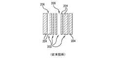
図1aに示すように、従来のナノインプリンティングリソグラフィプロセスは、複数の転写パターン202が形成されたインプリントスタンプ200を使用する。図1bに示すように、転写パターン202は簡単なラインと空間のパターンからなり、複数のライン204はライン間が空間206で分離されている。転写パターン202は基板211によって支持されている。インプリントスタンプ200を特別に設計されたマスク層203に押圧することにより(破線の矢印201を参照)、マスク層203の厚さが転写パターン202(図1aを参照されたい)に応じて変化し、転写パターン202がマスク層203に複製される。 As shown in FIG. 1a, a conventional nanoimprinting lithography process uses an
マスク層203は通常、ポリマーなどの材料から形成される。たとえば、マスク層203には、フォトレジスト材料を用いることができる。マスク層203は支持基板205上に堆積される。ステップ・アンド・リピートプロセスを用いて転写パターン202をマスク層203に繰り返し押圧し、マスク層203の全面が覆われるまで転写パターン202をマスク層203に複製する。 The
図2に示すように、このステップ・アンド・リピートプロセスにより、マスク層203には、転写パターン202に対して相補形状を成す複数の極小の圧痕207ができる。次に、図3に示すように、マスク層203を異方性エッチング(すなわち、極めて方向性の強いエッチング)を施し、マスク層203に極小パターン209を形成する。通常、支持基板205、またはマスク層203と支持基板205との間に設けられたもう1つの層(図示せず)が、異方性エッチングのエッチストップとして機能する。 As shown in FIG. 2, by this step-and-repeat process, a plurality of
図4では、各ライン204は、対向する側面204sと、上面204tと、対向する前面204fと、エッジ204eとを有する。各ライン204はライン間が空間206で分離されている。一般に、インプリントスタンプ200はシリコン(Si)などの材料から形成される。たとえば、基板211にはシリコンウェーハを用いることができ、ライン−空間機構(204、206)は、シリコン(Si)やポリシリコン(α−Si)から作成することができる。ナノインプリントスタンプの材料の選択としてシリコンを選択した理由は、シリコンを用いた構造および回路を製造するためのマイクロエレクトロニクスプロセスがしっかりと確立されており、シリコンは手頃な価格で容易に購入することができるからである。 In FIG. 4, each
しかしながら、従来のインプリントスタンプ200の欠点の1つは、シリコンが軟らかい物質であるため、マスク層203に押圧するステップの繰り返しにより、破損、損傷および摩耗を受けやすいことである。図4において、ライン204のE−Eの部分は、押圧するステップの繰り返しによる摩耗、破損、および損傷を特に受けやすい。図5は、図4のE−Eの部分の拡大図であり、エッジ204e、上面204t、側面204s、および前面204fが、マスク層203に対してわずか数回押圧しただけで、摩耗Wの影響を特に受けやすいことを示している。 However, one of the drawbacks of the
図6において、インプリントスタンプ200をマスク層203に押圧し(201)、ライン形状部204がマスク層203中に位置するようにする。押圧ステップの繰り返しによって、ライン形状部204のエッジ204eと上面204tに、符号Wで示すような摩耗、損傷、および破損が生じる。押圧ステップがわずか10回以下であっても、インプリントスタンプ200は、安定した、反復可能な、正確な転写パターン209を形成することができないところまで磨耗してしまう場合がある。 In FIG. 6, the
図7aおよび図7bはライン形状部204の摩耗を示す詳細図であり、ライン形状部204のエッジ204eおよび上面204tの部分はマスク層203と最初に接触する部分であり、押圧方向(201)に対して実質的に垂直な面を有しているので、それらの部分で摩耗が最も深刻であるということを示している。したがって、図8aおよび図8bに示すように、ライン形状部204は、マスク層203に対してわずか数回押圧しただけで、図8aに示す理想的なライン形状204から図8bに示す摩耗したライン形状204へと急激に劣化する。 7a and 7b are detailed views showing the wear of the line-
インプリントスタンプ200の製造は、インプリンティングリソグラフィプロセス全体の中で、最も重要で、最もコストのかかるステップの1つである。従来のインプリントスタンプ200のもう1つの欠点は、インプリントスタンプ200の製造コストを正当化するために必要な回数の押圧ステップを実施する前にインプリントスタンプ200が破損してしまったり、磨耗しきってしまったり、あるいはその両方が生じたりすることが原因で、インプリントスタンプ200の製造コストを回収することができない、ということである。したがって、従来のインプリントスタンプ200は製造が経済的でない。 The manufacture of
したがって、本発明の目的の一つは、摩耗、損傷、および破損に耐え得る極小のインプリントスタンプを提供することである。本発明の他の目的は、複数回の押圧ステップにわたって安定した、反復可能な、正確な転写パターン209が維持されるインプリントスタンプを提供し、製造コストを回収できるようにすることである。 Accordingly, one object of the present invention is to provide a minimal imprint stamp that can withstand abrasion, damage, and breakage. Another object of the present invention is to provide an imprint stamp in which a stable, repeatable and
本発明の微細成形炭化ケイ素ナノインプリントスタンプは、従来のナノインプリントスタンプに関する上記の欠点および制限を解決する。本発明の微細成形炭化ケイ素ナノインプリントスタンプは、従来のナノインプリントスタンプのシリコン材料と異なり、インプリントスタンプの材料として炭化ケイ素を用いるので、より強く、より丈夫である。 The micro-molded silicon carbide nanoimprint stamp of the present invention overcomes the above disadvantages and limitations associated with conventional nanoimprint stamps. Unlike the silicon material of the conventional nanoimprint stamp, the micro-molded silicon carbide nanoimprint stamp of the present invention uses silicon carbide as the material of the imprint stamp, so that it is stronger and stronger.
本発明の微細成形炭化ケイ素ナノインプリントスタンプは、耐用時間が長くなる。したがって、本発明の微細成形炭化ケイ素ナノインプリントスタンプは、シリコンから形成される従来のナノインプリントスタンプと異なり、摩耗、破損、あるいは損傷を生じることなく多数の押圧サイクルに耐えることができるので、その製造コストを回収することができる。 The micro-molded silicon carbide nanoimprint stamp of the present invention has a long service life. Therefore, unlike the conventional nanoimprint stamp formed from silicon, the micro-molded silicon carbide nanoimprint stamp of the present invention can withstand a large number of pressing cycles without causing wear, breakage, or damage, thereby reducing its manufacturing cost. It can be recovered.
本発明の他の態様および利点は、本発明の原理を例として示す添付の図面とともに、以下の詳細な説明から明らかになるであろう。 Other aspects and advantages of the present invention will become apparent from the following detailed description, taken in conjunction with the accompanying drawings, illustrating by way of example the principles of the invention.
以下に記載する詳細な説明および図面の幾つかにおいて、同一の構成要素は同一の符号で参照する。 In the detailed description and the drawings below, the same components are referred to with the same reference numerals.
例示目的の図面に示すように、本発明は、微細成形炭化ケイ素ナノインプリントスタンプ、または該炭化ケイ素ナノインプリントスタンプを微細成形する方法として実施される。この微細成形炭化ケイ素ナノインプリントスタンプは、ハンドリング基板と、ハンドリング基板に接続された接着層と、接着層に接続された基礎層とを含み、基礎層は、基準面と、基礎層に接続され基準面から外側に延びる複数の極小形状部とを有する。各極小形状部は、転写形状を画定する外面を有する。基礎層および極小形状部は全体が炭化ケイ素を含む材料から形成され、基礎層と極小形状部は完全に一体に微細成形される。すなわち、それらは単一要素すなわち一体として形成される。 As shown in the drawings for purposes of illustration, the present invention is practiced as a micromolded silicon carbide nanoimprint stamp or a method of micromolding the silicon carbide nanoimprint stamp. The micro-molded silicon carbide nanoimprint stamp includes a handling substrate, an adhesive layer connected to the handling substrate, and a base layer connected to the adhesive layer. The base layer is connected to the reference surface and the reference layer. And a plurality of minimally-shaped portions extending outward. Each minimally shaped portion has an outer surface that defines a transfer shape. The base layer and the minimum shape portion are entirely formed of a material containing silicon carbide, and the base layer and the minimum shape portion are completely formed into a single body. That is, they are formed as a single element or unity.
微細成形された炭化ケイ素製の極小形状部は、従来のナノインプリントスタンプのシリコン製の極小形状部よりも耐久性があり、弾性があり、硬いので、費用効率が高い。従って、本発明の微細成形炭化ケイ素ナノインプリントスタンプは、耐用時間が長く、その有効耐用時間が終わる前に製造コストを回収することができる。 The micro-molded silicon carbide micro-shaped part is more durable, elastic, and harder than the conventional nano-imprint stamp silicon mini-shaped part, which is cost effective. Therefore, the micro-molded silicon carbide nanoimprint stamp of the present invention has a long service life, and the manufacturing cost can be recovered before the effective service time ends.
本発明の炭化ケイ素(SiC)製の極小形状部はシリコン(Si)単体よりも硬い物質であり、押圧ステップを繰り返す間その転写形状を維持することができ、微細成形炭化ケイ素ナノインプリントスタンプによって転写される媒体に、反復可能な、安定した、寸法の正確な転写を行なうことができるので、本発明の炭化ケイ素ナノインプリントスタンプは従来のシリコン製ナノインプリントスタンプよりも正確である。 The silicon carbide (SiC) miniature portion of the present invention is a harder material than silicon (Si) alone, and can maintain its transferred shape during repeated pressing steps, and is transferred by a micro-molded silicon carbide nanoimprint stamp. The silicon carbide nanoimprint stamps of the present invention are more accurate than conventional silicon nanoimprint stamps because repeatable, stable, and accurate dimensional transfer can be performed on the media.
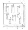
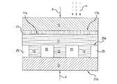
図9において、微細成形炭化ケイ素ナノインプリントスタンプ10は、ハンドリング基板15と、ハンドリング基板15に接続された接着層17と、接着層17に接続された基礎層11とを含む。基礎層11は、基準面13と、基礎層に接続され、基準面13から外側に延びる複数の極小形状部12とを有する。極小形状部12は、転写形状を画定する外面を有する。この転写形状は、極小形状部12間で同じものにしてもよいし、異なるものにしてもよい。たとえば、転写形状は極小形状部12の寸法によって決めることができ、極小形状部12の各々の幅W、長さL、および高さHなどにより決めることができる。極小形状部12が長方形の転写形状をもつものとして図示されているが、本発明を本明細書に例示した転写形状に限定されるものとして解釈すべきではなく、転写形状が長方形である必要はない。 In FIG. 9, the micro-molded silicon
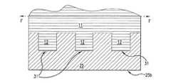
図9および図10は、微細成形炭化ケイ素ナノインプリントスタンプ10を用いて媒体(図示せず)に転写すべき転写パターンを画定する極小形状部12を、ベース表面13とともに示す図である。たとえば、極小形状部12間の空間Sは転写パターンの一部とすることができ、極小形状部12と空間Sによって媒体に転写すべきライン−空間パターンを画定するようになっている。 FIG. 9 and FIG. 10 are diagrams showing the
図10は、長方形または正方形の転写形状の場合、極小形状部12の外面が、対向する側面12sと、上面12tと、前面12fと、背面12bと、エッジ12eとを有することを示している。転写形状が長方形や正方形以外の形状である場合、極小形状部12は上記の表面を有しない場合もある。極小形状部12と基礎層11は、完全に一体になっている。すなわち、それらは、以下で説明するマイクロキャスティングプロセスにより一体として形成される単一要素である。極小形状部12と基礎層11はいずれも、炭化ケイ素(SiC)を含む材料から形成される。極小形状部12および基礎層11の材料は主に炭化ケイ素であるが、この炭化ケイ素は他の物質、すなわち微量の他の物質を含んでもよい。たとえば、この炭化ケイ素は、ドーパント物質として窒素(N)原子を含むことができる。 FIG. 10 shows that in the case of a rectangular or square transfer shape, the outer surface of the minimally shaped
ハンドリング基板15は、限定はしないが、ベアシリコンウェーハ、ポリシリコン(α−Si)コーティングシリコンウェーハ、シリコン酸化物(SiO2)コーティングシリコンウェーハ、窒化ケイ素(Si3N4)コーティングシリコンウェーハなど、種々の材料から形成することができる。マイクロエレクトロニクスの処理で使用される装置がシリコンウェーハを処理するのに非常に適しており、シリコンウェーハが容易に入手することができる低コストの材料であり、シリコンウェーハがウェーハ接合処理について優れた基板材料であるという理由から、ハンドリング基板15にシリコンウェーハを使用するのはよい選択である。The handling
ハンドリング基板15には種々の材料を用いることができるが、ハンドリング基板15は基礎層11を支持する必要があり、割れや歪みを生じることなく多数回の転写処理に耐えられるものでなければならないので、選択される材料は耐久性のある材料にする必要がある。また、ハンドリング基板15は、基礎層11、極小形状部12、および基準面13を破壊したり損傷させたりすることなく処理装置で取り扱うことができるものでなければならない。 Various materials can be used for the handling
接着層17には、限定はしないが、タングステン(W)、チタン(Ti)、窒化チタン(TiN)、コバルト(Co)、プラチナ(Pt)、金(Au)、金とスズの合金(AuSn)、銀(Ag)、およびそれらの金属をハンドリング基板15のシリコンでケイ化したケイ化物などの材料を用いることができる。たとえば、接着層17には、ケイ化タングステン(WSi2)を用いることができる。以下で説明するように、接着層17は、基礎層11とハンドリングウェーハ15とを機械的に接続するものである。ハンドリング基板15にシリコンを選択した場合、上記物質の中から1つを選択することにより、接着層17とハンドリング基板15との間の境界面に、ケイ化物接合を形成することができる。ウェーハ接合プロセスを用いてハンドリング基板15と基礎層11との間にそのケイ化物接合を形成し、接着層17が接合物質として働くようにすることが好ましい。The
極小形状部12、および極小形状部12間の空間Sの実際の寸法は、応用形態によって異なり、極小形状部12および空間Sを画定するために用いられるリソグラフィシステムのリソグラフィ限界によっても異なる。しかしながら、その寸法は約1.0μm未満であり、通常はナノメートルスケールであり、従って約100.0nm未満である。 The actual dimensions of the miniature features 12 and the space S between the miniature features 12 will vary depending on the application and will also depend on the lithography limits of the lithography system used to define the miniature features 12 and the space S. However, its dimensions are less than about 1.0 μm, usually on a nanometer scale, and therefore less than about 100.0 nm.
図11aにおいて、微細成形炭化ケイ素ナノインプリントスタンプ10によって転写される媒体50は、基板51によって支持されたインプリント媒体53を含む。微細成形炭化ケイ素ナノインプリントスタンプ10は、転写先の媒体53と接触された状態で押圧される(破線矢印Uを参照)。たとえば、微細成形炭化ケイ素ナノインプリントスタンプ10および/または媒体50は、互いに接触した状態で押圧することができる。使用する圧力の大きさは応用形態によって異なり、転写先の媒体53の材料によっても異なるであろう。たとえば、転写先の媒体53としては、フォトレジストなどのポリマー材料を用いることができる。 In FIG. 11 a, the medium 50 transferred by the micro-shaped silicon
図11bは、転写先の媒体53へ押圧されて接触状態になった微細成形炭化ケイ素ナノインプリントスタンプ10を示している。極小形状部12は、圧力の影響を受け、各々の外面全体にわたって磨耗される。特に、エッジ12e、対向する側面12s、上面12t、前面12f、背面12b、およびベース表面13などの様々な接触点CPの辺りが磨耗する。転写処理中は、約300psi〜約500psi(≒2068kPa〜2758kPa)以上の圧力にするのが一般的である。したがって、極小形状部12が摩耗、破損、または損傷する可能性は、本発明の微細成形炭化ケイ素ナノインプリントスタンプ10の硬い炭化ケイ素材料によって低減されるため、極小形状部12は、全般に摩耗に強く、特に上記の接触点CPの辺りで摩耗に強いものになっている。FIG. 11 b shows the micro-molded silicon
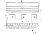
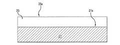
図12a〜図18は、炭化ケイ素ナノインプリントスタンプ10を微細成形する方法を示す図であり、基板21の表面21s上に離型層23を形成するステップを含んでいる。離型層23は、限定はしないが、化学蒸着堆積法(CVD)、物理蒸着堆積法(PVD)、およびスパッタリングなどの処理を用いて堆積させることができる。離型層23は、約数μm以下の厚さにすることができる。基板21には、限定はしないが、シリコン(Si)、単結晶シリコン、およびシリコンウェーハなどの材料を用いることができる。離型層23は、限定はしないが、表1に示す材料から形成することができる。 FIGS. 12 a to 18 are views showing a method of micro-molding the silicon

図12bにおいて、離型層23の表面23sに型枠層25を形成する。型枠層25の材料は、容易に堆積させることができ、容易にエッチングすることができ、さらにナノメートルスケールの形状でパターニングできるものでなければならない。型枠層25は実質的に平坦な基板21または離型層23の上に均一な堆積速度で堆積させ、型枠層25の表面25sが平滑で、実質的に平坦になるようにすることが好ましい。型枠層25は、限定はしないが、CVD、PVD、およびスパッタリングなどの処理を用いて堆積させることができる。型枠層25に適した材料としては、限定はしないが、表2に示す材料が挙げられる。 In FIG. 12 b, a
図12cでは、マスク24を用いて型枠層25にリソグラフのパターニングを施した後、エッチングを行い、離型層23まで延びる複数の極小の型穴31を形成している。離型層23の材料は、型枠層25をエッチングするのに使用される物質に対して離型層23がエッチストップとして働くような材料から選択することができる。 In FIG. 12 c, lithographic patterning is performed on the
たとえば、反応性イオンエッチング(RIE)などの等方性エッチングプロセスを用いて、極小の型穴31を形成することができる。反応性イオンエッチングは、極小の型穴31の垂直な側壁面を形成するのに非常に適していて、極小の型穴31内に形成される極小形状部12の所望の転写形状が長方形または正方形の転写形状である場合に特に適している。 For example, an extremely
型枠層25のパターニングは、周知のマイクロエレクトロニクス・フォトリソグラフィプロセスを用いて行なうことができる。たとえば、マスク24には、フォトレジスト材料からなるパターニングされた層を用いることができる。図13において、極小の型穴31は、型枠層の上面25sから離型層23の上面23sまで延びている。極小の型穴31の寸法は、同じものにしてもよいし、図13に示すように型穴間で異なるものにしてもよい。極小の型穴31の実際の寸法は、応用形態によって異なり、極小形状部12について上で述べたように、約1.0μm、好ましくは約100nm以下の寸法が、極小の型穴31の通常の値であろう。なぜなら、極小形状部12の転写形状は、極小形状部12を内部に微細成形する極小の型穴31によって決まるからである。 The patterning of the
図14aでは、極小の型穴31を炭化ケイ素(SiC)を含む材料で完全に充填している。極小の型穴31を満たしている炭化ケイ素の部分は複数の極小形状部12を形成している一方、炭化ケイ素の残りの部分は極小形状部12に接続された基礎層11を形成している。図14bでは、基礎層11を平坦化し(線F−Fを参照)、実質的に平坦な表面11sを形成している。化学機械平坦化(CMP)などのプロセスを用いて、基礎層11を平坦化し、線F−Fに沿って実質的に平坦な表面を形成することができる。 In FIG. 14a, the
図15では、基礎層11の平坦な表面11s上に接着層17が形成されている。接着層17は、限定はしないが、CVD、PVD、およびスパッタリングなどの処理を用いて堆積させることができる。接着層17に適した材料としては、限定はしないが、表3に示すような材料が挙げられる。 In FIG. 15, the
図16aにおいて、ハンドリング基板15と基板層21に圧力Pおよび熱hを加えることにより、ハンドリング基板15を接着層17に接合する。熱hおよび圧力Pは、接着層17が基礎層11とハンドリング基板15との間に機械的接合を形成するまで加え続ける。この接合を形成するのに必要となる圧力Pおよび熱hの大きさは、応用形態によって異なり、基礎層11、接着層17、およびハンドリング基板15に選択された材料によっても異なるであろう。たとえば、金−スズ(AuSn)合金ウェーハ接合の場合、圧力Pは4インチウェーハの全面にわたって約5,000lbs(即ち、≒64psi(≒441kPa))であり、加える熱hは約320℃である。別の例として、酸化物−酸化物ウェーハ接合の場合、加える熱hは約1100℃であり、圧力Pは約1気圧である(すなわち、圧力は加えない)。ハンドリング基板15に適した材料は、図9および図10を参照して上で説明した材料と同じである。 In FIG. 16 a, the handling
図16bでは、基板層21の背面21bにリソグラフのパターニングを施した後(たとえば、マスク28を通して)、エッチングを行い、離型層23まで延びる複数のスルーホール22を形成している。たとえば、反応性イオンエッチングを用いて、このスルーホール22を形成することができる。スルーホール22を形成した後、スルーホール22内にエッチング材を注入して離型層をエッチングによって除去し、基板層21を切り離す。離型層23のエッチングには、フッ化水素(HF)溶液または蒸気を用いることができる。たとえば、フッ化水素のエッチング液は、BSG、BPSG、PSG、TEOSなどの物質から形成されたシリコン酸化物(SiO2)製の離型層をエッチングすることができる。In FIG. 16 b, after lithographic patterning is performed on the
図17では、型枠層25の残りの部分をエッチングして、極小形状部12および基礎層11から型枠層25を除去している。型枠層25のエッチングには、フッ化水素(HF)溶液または蒸気を用いることができる。 In FIG. 17, the remaining part of the
図18は、型枠層25を除去した後に残るものが、本発明の微細成形炭化ケイ素ナノインプリントスタンプ10であることを示している。この微細成形炭化ケイ素ナノインプリントスタンプ10は、図11aおよび図11bを参照して先に説明したように、極小形状部12をインプリント媒体53に転写するために繰り返し用いることができる。転写処理の結果、極小形状部12によって、ナノメートルスケールの形状が転写先の媒体53に転写される。 FIG. 18 shows that what remains after removing the
図19a〜図22に示すように、本発明の一実施形態では、上記の離型層23を省略し、代わりに、図19aに示すように基板層21上に型枠層25を直に形成する場合がある。型枠層25の材料は、容易に堆積させることができ、容易にエッチングすることができ、さらにナノメートルスケールの形状をパターニングできるものでなければならない。型枠層25は基板21上に均一な堆積速度で堆積させ、型枠層の表面25sが平滑で、実質的に平坦になるようにすることが好ましい。 As shown in FIGS. 19a to 22, in one embodiment of the present invention, the
図19bでは、その後、型枠層25を上記のようにパターニングおよびエッチングして、基板層21まで延びる複数の極小の型穴31を形成している。基板層21は、型枠層25をエッチングするのに使用される物質に対して、エッチストップとして機能する。基板層21の材料は先に説明したものと同じ材料でよく、型枠層25は表2を参照して上で述べた材料から形成することができる。 In FIG. 19 b, the
図20では、極小の型穴31が基板層21まで延びていて、上で説明したように、極小の型穴31の寸法は、同じものにしてもよいし、型穴間で異なるものにしてもよい。 In FIG. 20, a
そして、図14a〜図16を参照して上で説明したのと同じようにして、型枠層25上に、炭化ケイ素を含む材料からなる基礎層11および複数の極小形状部12を形成する。基礎層11を平坦化した後、基礎層11の平坦な表面11s上に接着層17を形成する。次に、図21に示すように、ハンドリング基板15が接着層17に機械的に接合されるまで熱hおよび圧力Pを加えることにより、ハンドリング基板15を接着層17に接合する。接着層17の材料としては、表3を参照して上で述べたものと同じ材料を用いることができる。 Then, in the same manner as described above with reference to FIGS. 14 a to 16, the
図22において、基板層21が型枠層25から除去されるまで基板層21の背面21bを研削することにより、基板層21を型枠層25から除去することができる。たとえば、CMPのようなプロセスを用いて、基板層21を研削して除去することができる。次に、型枠層25を選択的エッチングによって除去し、基礎層11を切り離す。型枠層25のエッチングには、フッ化水素(HF)溶液または蒸気を用いることができる。 In FIG. 22, the
代替方法としては、基板層21の背面21bをパターニングし、その後エッチングして、その中に型枠層25まで延びる複数のスルーホール22を形成することにより、基板層21を型枠層25から除去することもできる(図16を参照)。次に、HFなどの選択性エッチング液をスルーホール22に注入し、型枠層25をエッチングすることにより、基板層21と、極小形状部12および基礎層11とを同様に切り離すことができる。図18に示すように、型枠層25を除去した後に残るのは、本発明の微細成形炭化ケイ素ナノインプリントスタンプ10である。 As an alternative, the
図23a〜図25に示すように、本発明のさらに別の実施形態では、実質的に平坦な表面25sを有する型枠層25にパターニング24を施し(図23aを参照)、その後エッチングし、その中に複数の極小の型穴31を形成する(図23bを参照)。型枠層25は、表2を参照して上で述べた材料から形成することができる。 As shown in FIGS. 23a to 25, in yet another embodiment of the present invention, patterning 24 is applied to a
図23cでは、上記のように極小の型穴31に炭化ケイ素を含む材料を充填することにより、複数の極小形状部12および基礎層11を形成している。その後、基礎層11を平坦化し(破線F−Fを参照)、その上に実質的に平坦な表面11sを形成する(図24を参照)。図24では、上記のように、実質的に平坦な表面11s上に接着層17を形成している。次に、図25aでは、同じく上記のように、熱hおよび圧力Pをかけることにより、ハンドリング基板15を接着層17に接合している。型枠層25が基礎層11から切り離されるまで、すなわち溶解されるまで、型枠層25を選択的にエッチングすることにより、型枠層25を基礎層11から除去することができる。型枠層25の材料の選択的エッチングには、ドライエッチングまたはウエットエッチングなどの選択性エッチングプロセスを用いることができる。代替方法として、図25bでは、型枠層25の背面25bを研削して(たとえば、CMPを用いて)型枠層25の厚さを減らし、型枠層25の薄い層だけが極小形状部12の上面12tを覆うようにしている。基礎層11から型枠層25の残りの部分を選択的に除去するのには、反応性イオンエッチング(RIE)などの選択性エッチングプロセスを用いることができる(図18を参照)。接着層17の材料としては、表3を参照して上で述べたものと同じ材料を用いることができる。また、ハンドリング基板15の材料も、上で述べたものと同じ材料を用いることができる。 In FIG. 23 c, a plurality of minimally shaped
本発明のいくつかの実施形態を開示および説明してきたが、本発明が説明および図示された特定の形態や部品配置に限定されることはない。本発明は特許請求の範囲によってのみ限定される。 While several embodiments of the present invention have been disclosed and described, the present invention is not limited to the specific forms or component arrangements described and illustrated. The invention is limited only by the claims.
10 本発明による微細成形炭化ケイ素ナノインプリントスタンプ
11 基礎層
12 極小形状部
13 基準面
15 ハンドリング基板
17 接着層
21 基板
22 スルーホール
23 離型層
25 型枠層
50 媒体
10 Micromolded Silicon
Claims (5)
Translated fromJapanese基板層(21)の上に離型層(23)を形成するステップと、
前記離型層(23)の上に型枠層(25)を形成するステップと、
前記型枠層(25)をパターニングした後エッチングして、前記離型層(23)まで延びる極小の型穴(31)を形成するステップと、
前記極小の型穴(31)に炭化ケイ素を充填することにより、複数の極小形状部(12)と、該極小形状部(12)に接続された基礎層(11)を形成するステップと、
前記基礎層(11)を平坦化して実質的に平坦な表面(11s)を形成するステップと、
前記基礎層(11)の平坦な表面(11s)上に接着層(17)を形成するステップと、
前記接着層(17)が、前記基礎層(11)及びハンドリング基板(15)との間に機械的接合を形成するまで、前記ハンドリング基板(15)及び前記基板層(21)に圧力P及び熱hを加えることにより、前記ハンドリング基板(15)を前記接着層(17)に接合するステップと、
前記基板層(21)の背面(21b)をパターニングした後エッチングして、前記離型層(23)まで延びる複数のスルーホール(22)を形成するステップと、
前記スルーホール(22)にエッチング剤を注入し、前記離型層(23)をエッチングして除去することで、前記基板層(21)を切り離すことにより、前記基板層(21)を取り除くステップと、
前記型枠層(25)をエッチングすることにより、前記極小形状部(12)及び前記基礎層(11)から前記型枠層(25)を除去するステップと、
からなる方法。A method of finely molding a silicon carbide nanoimprint stamp (10),
Forming a release layer (23) on the substrate layer (21);
Forming a mold layer (25) on the release layer (23);
Etching after patterning the mold layer (25) to form a minimal mold cavity (31) extending to the release layer (23);
Filling the minimal mold cavity (31) with silicon carbide to form a plurality of minimally-shaped portions (12) and a base layer (11) connected to the minimally-shaped portions (12);
Planarizing the base layer (11) to form a substantially flat surface (11s);
Forming an adhesive layer (17) on the flat surface (11s) of the base layer (11);
Until the adhesive layer (17) forms a mechanical bond between the base layer (11) and the handling substrate (15), pressure P and heat are applied to the handling substrate (15) and the substrate layer (21). bonding the handling substrate (15) to the adhesive layer (17) by adding h;
Etching after patterning the back surface (21b) of the substrate layer (21) to form a plurality of through holes (22) extending to the release layer (23);
Removing the substrate layer (21) by injecting an etchant into the through-hole (22) and removing the substrate layer (21) by etching and removing the release layer (23); ,
Etching the mold layer (25) to remove the mold layer (25) from the minimal shape portion (12) and the base layer (11);
A method consisting of:
基板層(21)上に型枠層(25)を形成するステップと、
前記型枠層(25)をパターニングした後エッチングして、前記基板層(21)まで延びる複数の極小の型穴(31)を形成するステップと、
前記極小の型穴(31)を炭化ケイ素を含む材料で充填することにより、複数の極小形状部(12)と、基礎層(11)とを形成するステップと、
前記基礎層(11)を平坦化して実質的に平坦な表面(11s)を形成するステップと、
前記基礎層(11)の平坦な表面(11s)上に接着層(17)を形成するステップと、
前記接着層(17)が、前記基礎層(11)及びハンドリング基板(15)との間に機械的接合を形成するまで、前記ハンドリング基板(15)及び前記基板層(21)に圧力P及び熱hを加えることにより、前記ハンドリング基板(15)を前記接着層(17)に接合するステップと、
前記型枠層(25)から前記基板層(21)を除去するステップと、
前記型枠層(25)をエッチングして、前記極小形状部(12)及び前記基礎層(11)から前記型枠層(25)を除去するステップと
を含み、
前記基板層(21)を除去するステップ、および前記型枠層(25)をエッチングして除去するステップは、
前記基板層(21)の背面(21b)をパターニングした後エッチングして、その中に前記型枠層(25)まで延びる複数のスルーホール(22)を形成するステップと、
前記スルーホール(22)にエッチング剤を注入して前記型枠層(25)をエッチングで取り除くことにより、前記基板層(21)を切り離すステップと
を含む方法。A method of finely molding a silicon carbide nanoprinting stamp (10),
Forming a mold layer (25) on the substrate layer (21);
Etching after patterning the mold layer (25) to form a plurality of minimal mold holes (31) extending to the substrate layer (21);
Filling the minimal mold cavity (31) with a material containing silicon carbide to form a plurality of minimally-shaped portions (12) and a base layer (11);
Planarizing the base layer (11) to form a substantially flat surface (11s);
Forming an adhesive layer (17) on the flat surface (11s) of the base layer (11);
Until the adhesive layer (17) forms a mechanical bond between the base layer (11) and the handling substrate (15), pressure P and heat are applied to the handling substrate (15) and the substrate layer (21). by adding h, a step of bonding the handling substrate (15) to said contactadhesive layer (17),
Removing the substrate layer (21) from the mold layer (25);
Etching the mold layer (25) to remove the mold layer (25) from the minimally-shaped portion (12) and the base layer (11),
Removing by etching step, and saidmold layer (25)removing saidsubstrate layer (21),
Etching after patterning the back surface (21b) of the substrate layer (21), and forming a plurality of through holes (22) extending to the mold layer (25) therein,
Separating the substrate layer (21) by injecting an etchant into the through hole (22) and removing the mold layer (25) by etching.
型枠層(25)をパターニングした後エッチングして、その中に複数の極小の型穴(31)を形成するステップと、
前記型穴(31)に炭化ケイ素を含む物質を充填することにより、複数の極小形状部(12)と、該複数の極小形状部に接続された基礎層(11)とを形成するステップと、
前記基礎層(11)を平坦化して実質的に平坦な表面(11s)を形成するステップと、
前記基礎層(11)の平坦な表面(11s)上に接着層(17)を形成するステップと、
前記接着層(17)が、前記基礎層(11)及びハンドリング基板(15)との間に機械的接合を形成するまで、前記ハンドリング基板(15)及び前記型枠層(25)に圧力P及び熱hを加えることにより、前記ハンドリング基板(15)を前記接着層(17)に接合するステップと、
前記基礎層(11)から前記型枠層(25)を除去するステップと
を含み、
前記型枠層(25)を除去するステップは、前記型枠層(25)を選択的にエッチングすることにより、前記基礎層(11)から前記型枠層(25)を切り離すステップを含み、
前記型枠層(25)は、前記極小形状部の上面が薄い層で覆われるところまで背面から研削され、前記選択的エッチングは、その後に実施されることからなる方法。A method of finely molding a silicon carbide nanoimprint stamp (10),
Etching after patterning the mold layer (25) to form a plurality of tiny mold cavities (31) therein;
Filling the mold cavity (31) with a substance containing silicon carbide to form a plurality of minimum shape portions (12) and a base layer (11) connected to the plurality of minimum shape portions;
Planarizing the base layer (11) to form a substantially flat surface (11s);
Forming an adhesive layer (17) on the flat surface (11s) of the base layer (11);
Until the adhesive layer (17) forms a mechanical bond between the base layer (11) and the handling substrate (15), the handling substrate (15) and the mold layer (25) are subjected to pressure P and Bonding the handling substrate (15) to the adhesive layer (17) by applying heat h;
Removing the formwork layer (25) from the base layer (11),
The step of removing the formwork layer (25) includes the step of separating the formwork layer (25) from the base layer (11) by selectively etching the formwork layer (25),
The mold layer (25) is ground from the back to the point where the top surface of the minimal feature is covered with a thin layer, and the selective etching is performed thereafter.
Applications Claiming Priority (1)
| Application Number | Priority Date | Filing Date | Title |
|---|---|---|---|
| US10/279,643US6755984B2 (en) | 2002-10-24 | 2002-10-24 | Micro-casted silicon carbide nano-imprinting stamp |
Publications (2)
| Publication Number | Publication Date |
|---|---|
| JP2004160647A JP2004160647A (en) | 2004-06-10 |
| JP4623955B2true JP4623955B2 (en) | 2011-02-02 |
Family
ID=32069360
Family Applications (1)
| Application Number | Title | Priority Date | Filing Date |
|---|---|---|---|
| JP2003364007AExpired - Fee RelatedJP4623955B2 (en) | 2002-10-24 | 2003-10-24 | Micro-molded silicon carbide nanoimprint stamp |
Country Status (5)
| Country | Link |
|---|---|
| US (2) | US6755984B2 (en) |
| EP (1) | EP1413923A3 (en) |
| JP (1) | JP4623955B2 (en) |
| CN (1) | CN1499289A (en) |
| TW (1) | TW200406834A (en) |
Families Citing this family (78)
| Publication number | Priority date | Publication date | Assignee | Title |
|---|---|---|---|---|
| US6916511B2 (en)* | 2002-10-24 | 2005-07-12 | Hewlett-Packard Development Company, L.P. | Method of hardening a nano-imprinting stamp |
| GB0227902D0 (en)* | 2002-11-29 | 2003-01-08 | Ingenia Holdings Ltd | Template |
| JP2004241397A (en)* | 2003-01-23 | 2004-08-26 | Dainippon Printing Co Ltd | Thin film transistor and manufacturing method thereof |
| US20060276043A1 (en)* | 2003-03-21 | 2006-12-07 | Johnson Mark A L | Method and systems for single- or multi-period edge definition lithography |
| WO2004086461A2 (en)* | 2003-03-21 | 2004-10-07 | North Carolina State University | Methods for nanoscale structures from optical lithography and subsequent lateral growth |
| ITTO20030473A1 (en)* | 2003-06-23 | 2004-12-24 | Infm Istituto Naz Per La Fisi Ca Della Mater | LITOGRAPHIC NANOIMPRESSION PROCEDURE WHICH PROVIDES THE USE OF A MOLD PRESENTING A REGION SUITABLE FOR |
| ES2383689T3 (en) | 2003-09-23 | 2012-06-25 | University Of North Carolina At Chapel Hill | Photocurable perfluoropolyethers for use as novel materials in microfluidic devices |
| US9040090B2 (en) | 2003-12-19 | 2015-05-26 | The University Of North Carolina At Chapel Hill | Isolated and fixed micro and nano structures and methods thereof |
| EP3242318A1 (en) | 2003-12-19 | 2017-11-08 | The University of North Carolina at Chapel Hill | Monodisperse micro-structure or nano-structure product |
| US7060625B2 (en)* | 2004-01-27 | 2006-06-13 | Hewlett-Packard Development Company, L.P. | Imprint stamp |
| WO2007021762A2 (en) | 2005-08-09 | 2007-02-22 | The University Of North Carolina At Chapel Hill | Methods and materials for fabricating microfluidic devices |
| WO2005084191A2 (en)* | 2004-02-13 | 2005-09-15 | The University Of North Carolina At Chapel Hill | Functional materials and novel methods for the fabrication of microfluidic devices |
| US7730834B2 (en)* | 2004-03-04 | 2010-06-08 | Asml Netherlands B.V. | Printing apparatus and device manufacturing method |
| CN100555076C (en)* | 2004-07-26 | 2009-10-28 | 鸿富锦精密工业(深圳)有限公司 | Be used for pressing mold of nano impression and preparation method thereof |
| US20060105550A1 (en)* | 2004-11-17 | 2006-05-18 | Manish Sharma | Method of depositing material on a substrate for a device |
| CN1300635C (en)* | 2004-12-09 | 2007-02-14 | 上海交通大学 | Vacuum negative pressure nanometer press printing method |
| US7676088B2 (en) | 2004-12-23 | 2010-03-09 | Asml Netherlands B.V. | Imprint lithography |
| US20060144274A1 (en)* | 2004-12-30 | 2006-07-06 | Asml Netherlands B.V. | Imprint lithography |
| US7490547B2 (en)* | 2004-12-30 | 2009-02-17 | Asml Netherlands B.V. | Imprint lithography |
| US20060144814A1 (en)* | 2004-12-30 | 2006-07-06 | Asml Netherlands B.V. | Imprint lithography |
| US7686970B2 (en)* | 2004-12-30 | 2010-03-30 | Asml Netherlands B.V. | Imprint lithography |
| US7354698B2 (en)* | 2005-01-07 | 2008-04-08 | Asml Netherlands B.V. | Imprint lithography |
| US8695501B2 (en)* | 2005-01-28 | 2014-04-15 | Hewlett-Packard Development Company, L.P. | Method of forming a contact printing stamp |
| US7374968B2 (en)* | 2005-01-28 | 2008-05-20 | Hewlett-Packard Development Company, L.P. | Method of utilizing a contact printing stamp |
| US20060169592A1 (en)* | 2005-01-31 | 2006-08-03 | Hewlett-Packard Development Company, L.P. | Periodic layered structures and methods therefor |
| EP1853967A4 (en)* | 2005-02-03 | 2009-11-11 | Univ North Carolina | LOW-VOLTAGE SURFACE-VOLTAGE POLYMER MATERIAL FOR USE IN LIQUID CRYSTAL DISPLAY DEVICES |
| US7922474B2 (en)* | 2005-02-17 | 2011-04-12 | Asml Netherlands B.V. | Imprint lithography |
| US7291282B2 (en)* | 2005-03-01 | 2007-11-06 | Hewlett-Packard Development Company, L.P. | Method of fabricating a mold for imprinting a structure |
| US7523701B2 (en)* | 2005-03-07 | 2009-04-28 | Asml Netherlands B.V. | Imprint lithography method and apparatus |
| TWI280159B (en)* | 2005-03-29 | 2007-05-01 | Li Bing Huan | Method for fabricating nano-adhesive |
| US7762186B2 (en)* | 2005-04-19 | 2010-07-27 | Asml Netherlands B.V. | Imprint lithography |
| US7611348B2 (en)* | 2005-04-19 | 2009-11-03 | Asml Netherlands B.V. | Imprint lithography |
| US7442029B2 (en)* | 2005-05-16 | 2008-10-28 | Asml Netherlands B.V. | Imprint lithography |
| US7692771B2 (en)* | 2005-05-27 | 2010-04-06 | Asml Netherlands B.V. | Imprint lithography |
| US7708924B2 (en)* | 2005-07-21 | 2010-05-04 | Asml Netherlands B.V. | Imprint lithography |
| US20060267231A1 (en)* | 2005-05-27 | 2006-11-30 | Asml Netherlands B.V. | Imprint lithography |
| US7700498B2 (en)* | 2005-05-27 | 2010-04-20 | Princeton University | Self-repair and enhancement of nanostructures by liquification under guiding conditions |
| US7418902B2 (en)* | 2005-05-31 | 2008-09-02 | Asml Netherlands B.V. | Imprint lithography including alignment |
| US7377764B2 (en)* | 2005-06-13 | 2008-05-27 | Asml Netherlands B.V. | Imprint lithography |
| US20070023976A1 (en)* | 2005-07-26 | 2007-02-01 | Asml Netherlands B.V. | Imprint lithography |
| WO2007133235A2 (en)* | 2005-08-08 | 2007-11-22 | Liquidia Technologies, Inc. | Micro and nano-structure metrology |
| KR101171190B1 (en) | 2005-11-02 | 2012-08-06 | 삼성전자주식회사 | Manufacturing method of dsplay device and mold therefor |
| US7878791B2 (en)* | 2005-11-04 | 2011-02-01 | Asml Netherlands B.V. | Imprint lithography |
| US8011915B2 (en)* | 2005-11-04 | 2011-09-06 | Asml Netherlands B.V. | Imprint lithography |
| FR2893018B1 (en)* | 2005-11-09 | 2008-03-14 | Commissariat Energie Atomique | METHOD OF FORMING MEDIA HAVING PATTERNS, SUCH AS LITHOGRAPHIC MASKS |
| US7517211B2 (en) | 2005-12-21 | 2009-04-14 | Asml Netherlands B.V. | Imprint lithography |
| US20070138699A1 (en)* | 2005-12-21 | 2007-06-21 | Asml Netherlands B.V. | Imprint lithography |
| TW200734197A (en)* | 2006-03-02 | 2007-09-16 | Univ Nat Cheng Kung | Pattern printing transfer process for macromolecule resist of non-solvent liquid |
| JP4997811B2 (en)* | 2006-03-31 | 2012-08-08 | 大日本印刷株式会社 | Mold and mold manufacturing method |
| US8015939B2 (en)* | 2006-06-30 | 2011-09-13 | Asml Netherlands B.V. | Imprintable medium dispenser |
| US8318253B2 (en)* | 2006-06-30 | 2012-11-27 | Asml Netherlands B.V. | Imprint lithography |
| WO2008011051A1 (en)* | 2006-07-17 | 2008-01-24 | Liquidia Technologies, Inc. | Nanoparticle fabrication methods, systems, and materials |
| KR100889814B1 (en) | 2006-07-25 | 2009-03-20 | 삼성전자주식회사 | Stamper, manufacturing method and imprinting process of substrate using stamper |
| KR100831046B1 (en)* | 2006-09-13 | 2008-05-21 | 삼성전자주식회사 | Nano imprint mold and its manufacturing method |
| US7388661B2 (en)* | 2006-10-20 | 2008-06-17 | Hewlett-Packard Development Company, L.P. | Nanoscale structures, systems, and methods for use in nano-enhanced raman spectroscopy (NERS) |
| US7391511B1 (en) | 2007-01-31 | 2008-06-24 | Hewlett-Packard Development Company, L.P. | Raman signal-enhancing structures and Raman spectroscopy systems including such structures |
| US20100151031A1 (en)* | 2007-03-23 | 2010-06-17 | Desimone Joseph M | Discrete size and shape specific organic nanoparticles designed to elicit an immune response |
| JP2010537395A (en)* | 2007-05-30 | 2010-12-02 | モレキュラー・インプリンツ・インコーポレーテッド | Template with silicon nitride, silicon carbide, or silicon oxynitride film |
| US7758981B2 (en)* | 2007-07-25 | 2010-07-20 | Hitachi Global Storage Technologies Netherlands B.V. | Method for making a master disk for nanoimprinting patterned magnetic recording disks, master disk made by the method, and disk imprinted by the master disk |
| US20090038636A1 (en)* | 2007-08-09 | 2009-02-12 | Asml Netherlands B.V. | Cleaning method |
| TWI357886B (en) | 2007-08-13 | 2012-02-11 | Epistar Corp | Stamp having nanometer scale structure and applica |
| US7854877B2 (en) | 2007-08-14 | 2010-12-21 | Asml Netherlands B.V. | Lithography meandering order |
| US8144309B2 (en) | 2007-09-05 | 2012-03-27 | Asml Netherlands B.V. | Imprint lithography |
| CN101135842B (en)* | 2007-10-25 | 2011-11-02 | 复旦大学 | Method for copying nano autogram formwork |
| CN101487974B (en)* | 2008-01-17 | 2013-06-12 | 晶元光电股份有限公司 | A nanoscale imprint structure and its application in light-emitting elements |
| WO2009113063A2 (en) | 2008-03-10 | 2009-09-17 | Yeda Research & Development Company Ltd. N | Method for fabricating nano-scale patterned surfaces |
| US8003236B2 (en)* | 2008-06-17 | 2011-08-23 | Hitachi Global Storage Technologies Netherlands B.V. | Method for making a master mold with high bit-aspect-ratio for nanoimprinting patterned magnetic recording disks, master mold made by the method, and disk imprinted by the master mold |
| US8119017B2 (en)* | 2008-06-17 | 2012-02-21 | Hitachi Global Storage Technologies Netherlands B.V. | Method using block copolymers for making a master mold with high bit-aspect-ratio for nanoimprinting patterned magnetic recording disks |
| US7976715B2 (en)* | 2008-06-17 | 2011-07-12 | Hitachi Global Storage Technologies Netherlands B.V. | Method using block copolymers for making a master mold with high bit-aspect-ratio for nanoimprinting patterned magnetic recording disks |
| KR20110055586A (en)* | 2008-08-05 | 2011-05-25 | 스몰텍 에이비 | Manufacturing method of high aspect ratio template for template and lithography and use of template to drill substrate in nanoscale |
| US8633501B2 (en) | 2008-08-12 | 2014-01-21 | Epistar Corporation | Light-emitting device having a patterned surface |
| JP2010157536A (en)* | 2008-12-26 | 2010-07-15 | Nuflare Technology Inc | Method for manufacturing susceptor |
| US8059350B2 (en)* | 2009-10-22 | 2011-11-15 | Hitachi Global Storage Technologies Netherlands B.V. | Patterned magnetic recording disk with patterned servo sectors having chevron servo patterns |
| JP5599213B2 (en)* | 2010-03-30 | 2014-10-01 | Hoya株式会社 | Mold manufacturing method |
| US8293645B2 (en) | 2010-06-30 | 2012-10-23 | Taiwan Semiconductor Manufacturing Co., Ltd. | Method for forming photovoltaic cell |
| CN104597719B (en)* | 2015-01-12 | 2016-09-14 | 北京同方生物芯片技术有限公司 | Nickel positive mold manufacture method based on positive photoresist |
| DE102016110429A1 (en) | 2016-06-06 | 2017-12-07 | Infineon Technologies Ag | Energy filter for processing a power semiconductor device |
| DE102016110523B4 (en) | 2016-06-08 | 2023-04-06 | Infineon Technologies Ag | Processing a power semiconductor device |
Family Cites Families (12)
| Publication number | Priority date | Publication date | Assignee | Title |
|---|---|---|---|---|
| US3973495A (en)* | 1970-07-31 | 1976-08-10 | Vuestamp International Proprietary Limited | Hand stamp |
| JPH08175099A (en)* | 1994-12-27 | 1996-07-09 | Ogura Print:Kk | Transfer sheet, method of forming the same, and base film for the transfer sheet |
| US6309580B1 (en)* | 1995-11-15 | 2001-10-30 | Regents Of The University Of Minnesota | Release surfaces, particularly for use in nanoimprint lithography |
| JPH10133223A (en)* | 1996-10-31 | 1998-05-22 | Denso Corp | Laminated type liquid crystal cell and its manufacture |
| US6199269B1 (en)* | 1997-10-23 | 2001-03-13 | International Business Machines Corporation | Manipulation of micromechanical objects |
| JP3860348B2 (en)* | 1998-11-19 | 2006-12-20 | ローム株式会社 | Thermal print head and manufacturing method thereof |
| US6312612B1 (en)* | 1999-06-09 | 2001-11-06 | The Procter & Gamble Company | Apparatus and method for manufacturing an intracutaneous microneedle array |
| US6521324B1 (en)* | 1999-11-30 | 2003-02-18 | 3M Innovative Properties Company | Thermal transfer of microstructured layers |
| JP3999436B2 (en)* | 2000-03-10 | 2007-10-31 | 富士フイルム株式会社 | Master carrier for magnetic transfer |
| JP4431287B2 (en)* | 2001-02-05 | 2010-03-10 | パイオニア株式会社 | Manufacturing method of optical disk |
| US20020153625A1 (en)* | 2001-02-05 | 2002-10-24 | Pioneer Corporation | Stamper-forming electrode material, stamper-forming thin film, and method of manufacturing optical disk |
| US20030071016A1 (en)* | 2001-10-11 | 2003-04-17 | Wu-Sheng Shih | Patterned structure reproduction using nonsticking mold |
- 2002
- 2002-10-24USUS10/279,643patent/US6755984B2/ennot_activeExpired - Fee Related
- 2003
- 2003-05-23TWTW092114036Apatent/TW200406834A/enunknown
- 2003-07-24CNCNA031330770Apatent/CN1499289A/enactivePending
- 2003-10-03EPEP03256271Apatent/EP1413923A3/ennot_activeWithdrawn
- 2003-10-24JPJP2003364007Apatent/JP4623955B2/ennot_activeExpired - Fee Related
- 2004
- 2004-03-05USUS10/794,928patent/US7080596B2/ennot_activeExpired - Fee Related
Also Published As
| Publication number | Publication date |
|---|---|
| US7080596B2 (en) | 2006-07-25 |
| US20040169003A1 (en) | 2004-09-02 |
| CN1499289A (en) | 2004-05-26 |
| EP1413923A2 (en) | 2004-04-28 |
| US6755984B2 (en) | 2004-06-29 |
| US20040081800A1 (en) | 2004-04-29 |
| EP1413923A3 (en) | 2006-05-17 |
| TW200406834A (en) | 2004-05-01 |
| JP2004160647A (en) | 2004-06-10 |
Similar Documents
| Publication | Publication Date | Title |
|---|---|---|
| JP4623955B2 (en) | Micro-molded silicon carbide nanoimprint stamp | |
| TWI300237B (en) | Hardened nano-imprinting stamp | |
| JP4005927B2 (en) | Nano-size imprint stamps using spacer technology | |
| US6759180B2 (en) | Method of fabricating sub-lithographic sized line and space patterns for nano-imprinting lithography | |
| US20120189780A1 (en) | Controlling Thickness of Residual Layer | |
| JP2008290316A (en) | Pattern forming method, pattern formed by the pattern forming method, mold, processing apparatus, and processing method | |
| JP2006205352A (en) | Method for manufacturing MEMS structure | |
| JP2011165855A (en) | Pattern forming method | |
| US7462292B2 (en) | Silicon carbide imprint stamp | |
| US7060625B2 (en) | Imprint stamp | |
| US20150027063A1 (en) | Method for fabricating pad conditioning tool | |
| JP2005522689A5 (en) | ||
| CN118545678A (en) | Preparation method of MEMS cavity structure | |
| US8979613B2 (en) | Nano-fabricated structured diamond abrasive article | |
| JP2007320246A (en) | Mold and mold manufacturing method | |
| CN114843177B (en) | Manufacturing method of groove Schottky structure | |
| JP4845564B2 (en) | Pattern transfer method | |
| KR20140122860A (en) | Method of manufacturing an adhesion pad | |
| HK1064749A (en) | Micro-casted silicon carbide nano-imprinting stamp | |
| CN112198759A (en) | Imprint mold, manufacturing method of imprint mold, and nanoimprint method | |
| JP4942131B2 (en) | Stamper and nanostructure transfer method using the same | |
| JP2005313647A (en) | Molds for nanoprinting, methods for producing such molds, and methods of using such molds | |
| KR100520488B1 (en) | Nano imprinting stamp and manufacturing method of the same | |
| JP5653574B2 (en) | Nanoprinted device with metal pattern and method for nanoprinting metal pattern | |
| CN100373259C (en) | Imprinting method for patterns with the smallest size in the nanoscale |
Legal Events
| Date | Code | Title | Description |
|---|---|---|---|
| A621 | Written request for application examination | Free format text:JAPANESE INTERMEDIATE CODE: A621 Effective date:20060720 | |
| A131 | Notification of reasons for refusal | Free format text:JAPANESE INTERMEDIATE CODE: A131 Effective date:20090120 | |
| A601 | Written request for extension of time | Free format text:JAPANESE INTERMEDIATE CODE: A601 Effective date:20090420 | |
| A602 | Written permission of extension of time | Free format text:JAPANESE INTERMEDIATE CODE: A602 Effective date:20090423 | |
| A521 | Request for written amendment filed | Free format text:JAPANESE INTERMEDIATE CODE: A523 Effective date:20090717 | |
| A131 | Notification of reasons for refusal | Free format text:JAPANESE INTERMEDIATE CODE: A131 Effective date:20090818 | |
| A601 | Written request for extension of time | Free format text:JAPANESE INTERMEDIATE CODE: A601 Effective date:20091118 | |
| A602 | Written permission of extension of time | Free format text:JAPANESE INTERMEDIATE CODE: A602 Effective date:20091124 | |
| A521 | Request for written amendment filed | Free format text:JAPANESE INTERMEDIATE CODE: A523 Effective date:20100218 | |
| TRDD | Decision of grant or rejection written | ||
| A01 | Written decision to grant a patent or to grant a registration (utility model) | Free format text:JAPANESE INTERMEDIATE CODE: A01 Effective date:20101012 | |
| A01 | Written decision to grant a patent or to grant a registration (utility model) | Free format text:JAPANESE INTERMEDIATE CODE: A01 | |
| A61 | First payment of annual fees (during grant procedure) | Free format text:JAPANESE INTERMEDIATE CODE: A61 Effective date:20101102 | |
| R150 | Certificate of patent or registration of utility model | Ref document number:4623955 Country of ref document:JP Free format text:JAPANESE INTERMEDIATE CODE: R150 Free format text:JAPANESE INTERMEDIATE CODE: R150 | |
| FPAY | Renewal fee payment (event date is renewal date of database) | Free format text:PAYMENT UNTIL: 20131112 Year of fee payment:3 | |
| R250 | Receipt of annual fees | Free format text:JAPANESE INTERMEDIATE CODE: R250 | |
| R250 | Receipt of annual fees | Free format text:JAPANESE INTERMEDIATE CODE: R250 | |
| S111 | Request for change of ownership or part of ownership | Free format text:JAPANESE INTERMEDIATE CODE: R313113 | |
| R350 | Written notification of registration of transfer | Free format text:JAPANESE INTERMEDIATE CODE: R350 | |
| R250 | Receipt of annual fees | Free format text:JAPANESE INTERMEDIATE CODE: R250 | |
| R250 | Receipt of annual fees | Free format text:JAPANESE INTERMEDIATE CODE: R250 | |
| R250 | Receipt of annual fees | Free format text:JAPANESE INTERMEDIATE CODE: R250 | |
| R250 | Receipt of annual fees | Free format text:JAPANESE INTERMEDIATE CODE: R250 | |
| LAPS | Cancellation because of no payment of annual fees |