JP4605554B2 - Mask material for dry etching - Google Patents
Mask material for dry etchingDownload PDFInfo
- Publication number
- JP4605554B2 JP4605554B2JP2000224248AJP2000224248AJP4605554B2JP 4605554 B2JP4605554 B2JP 4605554B2JP 2000224248 AJP2000224248 AJP 2000224248AJP 2000224248 AJP2000224248 AJP 2000224248AJP 4605554 B2JP4605554 B2JP 4605554B2
- Authority
- JP
- Japan
- Prior art keywords
- etching
- gas
- mask
- film
- layer
- Prior art date
- Legal status (The legal status is an assumption and is not a legal conclusion. Google has not performed a legal analysis and makes no representation as to the accuracy of the status listed.)
- Expired - Lifetime
Links
Images


Classifications
- C—CHEMISTRY; METALLURGY
- C23—COATING METALLIC MATERIAL; COATING MATERIAL WITH METALLIC MATERIAL; CHEMICAL SURFACE TREATMENT; DIFFUSION TREATMENT OF METALLIC MATERIAL; COATING BY VACUUM EVAPORATION, BY SPUTTERING, BY ION IMPLANTATION OR BY CHEMICAL VAPOUR DEPOSITION, IN GENERAL; INHIBITING CORROSION OF METALLIC MATERIAL OR INCRUSTATION IN GENERAL
- C23F—NON-MECHANICAL REMOVAL OF METALLIC MATERIAL FROM SURFACE; INHIBITING CORROSION OF METALLIC MATERIAL OR INCRUSTATION IN GENERAL; MULTI-STEP PROCESSES FOR SURFACE TREATMENT OF METALLIC MATERIAL INVOLVING AT LEAST ONE PROCESS PROVIDED FOR IN CLASS C23 AND AT LEAST ONE PROCESS COVERED BY SUBCLASS C21D OR C22F OR CLASS C25
- C23F4/00—Processes for removing metallic material from surfaces, not provided for in group C23F1/00 or C23F3/00
- B—PERFORMING OPERATIONS; TRANSPORTING
- B82—NANOTECHNOLOGY
- B82Y—SPECIFIC USES OR APPLICATIONS OF NANOSTRUCTURES; MEASUREMENT OR ANALYSIS OF NANOSTRUCTURES; MANUFACTURE OR TREATMENT OF NANOSTRUCTURES
- B82Y10/00—Nanotechnology for information processing, storage or transmission, e.g. quantum computing or single electron logic
- B—PERFORMING OPERATIONS; TRANSPORTING
- B82—NANOTECHNOLOGY
- B82Y—SPECIFIC USES OR APPLICATIONS OF NANOSTRUCTURES; MEASUREMENT OR ANALYSIS OF NANOSTRUCTURES; MANUFACTURE OR TREATMENT OF NANOSTRUCTURES
- B82Y25/00—Nanomagnetism, e.g. magnetoimpedance, anisotropic magnetoresistance, giant magnetoresistance or tunneling magnetoresistance
- B—PERFORMING OPERATIONS; TRANSPORTING
- B82—NANOTECHNOLOGY
- B82Y—SPECIFIC USES OR APPLICATIONS OF NANOSTRUCTURES; MEASUREMENT OR ANALYSIS OF NANOSTRUCTURES; MANUFACTURE OR TREATMENT OF NANOSTRUCTURES
- B82Y40/00—Manufacture or treatment of nanostructures
- G—PHYSICS
- G11—INFORMATION STORAGE
- G11B—INFORMATION STORAGE BASED ON RELATIVE MOVEMENT BETWEEN RECORD CARRIER AND TRANSDUCER
- G11B5/00—Recording by magnetisation or demagnetisation of a record carrier; Reproducing by magnetic means; Record carriers therefor
- G11B5/127—Structure or manufacture of heads, e.g. inductive
- G11B5/33—Structure or manufacture of flux-sensitive heads, i.e. for reproduction only; Combination of such heads with means for recording or erasing only
- G11B5/39—Structure or manufacture of flux-sensitive heads, i.e. for reproduction only; Combination of such heads with means for recording or erasing only using magneto-resistive devices or effects
- G11B5/3903—Structure or manufacture of flux-sensitive heads, i.e. for reproduction only; Combination of such heads with means for recording or erasing only using magneto-resistive devices or effects using magnetic thin film layers or their effects, the films being part of integrated structures
- G11B5/3906—Details related to the use of magnetic thin film layers or to their effects
- G11B5/3909—Arrangements using a magnetic tunnel junction
- H—ELECTRICITY
- H01—ELECTRIC ELEMENTS
- H01F—MAGNETS; INDUCTANCES; TRANSFORMERS; SELECTION OF MATERIALS FOR THEIR MAGNETIC PROPERTIES
- H01F41/00—Apparatus or processes specially adapted for manufacturing or assembling magnets, inductances or transformers; Apparatus or processes specially adapted for manufacturing materials characterised by their magnetic properties
- H01F41/14—Apparatus or processes specially adapted for manufacturing or assembling magnets, inductances or transformers; Apparatus or processes specially adapted for manufacturing materials characterised by their magnetic properties for applying magnetic films to substrates
- H01F41/30—Apparatus or processes specially adapted for manufacturing or assembling magnets, inductances or transformers; Apparatus or processes specially adapted for manufacturing materials characterised by their magnetic properties for applying magnetic films to substrates for applying nanostructures, e.g. by molecular beam epitaxy [MBE]
- H01F41/302—Apparatus or processes specially adapted for manufacturing or assembling magnets, inductances or transformers; Apparatus or processes specially adapted for manufacturing materials characterised by their magnetic properties for applying magnetic films to substrates for applying nanostructures, e.g. by molecular beam epitaxy [MBE] for applying spin-exchange-coupled multilayers, e.g. nanostructured superlattices
- H01F41/308—Apparatus or processes specially adapted for manufacturing or assembling magnets, inductances or transformers; Apparatus or processes specially adapted for manufacturing materials characterised by their magnetic properties for applying magnetic films to substrates for applying nanostructures, e.g. by molecular beam epitaxy [MBE] for applying spin-exchange-coupled multilayers, e.g. nanostructured superlattices lift-off processes, e.g. ion milling, for trimming or patterning
- H—ELECTRICITY
- H01—ELECTRIC ELEMENTS
- H01L—SEMICONDUCTOR DEVICES NOT COVERED BY CLASS H10
- H01L21/00—Processes or apparatus adapted for the manufacture or treatment of semiconductor or solid state devices or of parts thereof
- H01L21/02—Manufacture or treatment of semiconductor devices or of parts thereof
- H01L21/027—Making masks on semiconductor bodies for further photolithographic processing not provided for in group H01L21/18 or H01L21/34
- H01L21/033—Making masks on semiconductor bodies for further photolithographic processing not provided for in group H01L21/18 or H01L21/34 comprising inorganic layers
- H01L21/0332—Making masks on semiconductor bodies for further photolithographic processing not provided for in group H01L21/18 or H01L21/34 comprising inorganic layers characterised by their composition, e.g. multilayer masks, materials
- H—ELECTRICITY
- H01—ELECTRIC ELEMENTS
- H01L—SEMICONDUCTOR DEVICES NOT COVERED BY CLASS H10
- H01L21/00—Processes or apparatus adapted for the manufacture or treatment of semiconductor or solid state devices or of parts thereof
- H01L21/02—Manufacture or treatment of semiconductor devices or of parts thereof
- H01L21/04—Manufacture or treatment of semiconductor devices or of parts thereof the devices having potential barriers, e.g. a PN junction, depletion layer or carrier concentration layer
- H01L21/18—Manufacture or treatment of semiconductor devices or of parts thereof the devices having potential barriers, e.g. a PN junction, depletion layer or carrier concentration layer the devices having semiconductor bodies comprising elements of Group IV of the Periodic Table or AIIIBV compounds with or without impurities, e.g. doping materials
- H01L21/30—Treatment of semiconductor bodies using processes or apparatus not provided for in groups H01L21/20 - H01L21/26
- H01L21/31—Treatment of semiconductor bodies using processes or apparatus not provided for in groups H01L21/20 - H01L21/26 to form insulating layers thereon, e.g. for masking or by using photolithographic techniques; After treatment of these layers; Selection of materials for these layers
- H01L21/3205—Deposition of non-insulating-, e.g. conductive- or resistive-, layers on insulating layers; After-treatment of these layers
- H01L21/321—After treatment
- H01L21/3213—Physical or chemical etching of the layers, e.g. to produce a patterned layer from a pre-deposited extensive layer
- H01L21/32133—Physical or chemical etching of the layers, e.g. to produce a patterned layer from a pre-deposited extensive layer by chemical means only
- H01L21/32135—Physical or chemical etching of the layers, e.g. to produce a patterned layer from a pre-deposited extensive layer by chemical means only by vapour etching only
- H01L21/32136—Physical or chemical etching of the layers, e.g. to produce a patterned layer from a pre-deposited extensive layer by chemical means only by vapour etching only using plasmas
- H—ELECTRICITY
- H01—ELECTRIC ELEMENTS
- H01L—SEMICONDUCTOR DEVICES NOT COVERED BY CLASS H10
- H01L21/00—Processes or apparatus adapted for the manufacture or treatment of semiconductor or solid state devices or of parts thereof
- H01L21/02—Manufacture or treatment of semiconductor devices or of parts thereof
- H01L21/04—Manufacture or treatment of semiconductor devices or of parts thereof the devices having potential barriers, e.g. a PN junction, depletion layer or carrier concentration layer
- H01L21/18—Manufacture or treatment of semiconductor devices or of parts thereof the devices having potential barriers, e.g. a PN junction, depletion layer or carrier concentration layer the devices having semiconductor bodies comprising elements of Group IV of the Periodic Table or AIIIBV compounds with or without impurities, e.g. doping materials
- H01L21/30—Treatment of semiconductor bodies using processes or apparatus not provided for in groups H01L21/20 - H01L21/26
- H01L21/31—Treatment of semiconductor bodies using processes or apparatus not provided for in groups H01L21/20 - H01L21/26 to form insulating layers thereon, e.g. for masking or by using photolithographic techniques; After treatment of these layers; Selection of materials for these layers
- H01L21/3205—Deposition of non-insulating-, e.g. conductive- or resistive-, layers on insulating layers; After-treatment of these layers
- H01L21/321—After treatment
- H01L21/3213—Physical or chemical etching of the layers, e.g. to produce a patterned layer from a pre-deposited extensive layer
- H01L21/32139—Physical or chemical etching of the layers, e.g. to produce a patterned layer from a pre-deposited extensive layer using masks
- H—ELECTRICITY
- H10—SEMICONDUCTOR DEVICES; ELECTRIC SOLID-STATE DEVICES NOT OTHERWISE PROVIDED FOR
- H10N—ELECTRIC SOLID-STATE DEVICES NOT OTHERWISE PROVIDED FOR
- H10N50/00—Galvanomagnetic devices
- H10N50/01—Manufacture or treatment
- G—PHYSICS
- G11—INFORMATION STORAGE
- G11B—INFORMATION STORAGE BASED ON RELATIVE MOVEMENT BETWEEN RECORD CARRIER AND TRANSDUCER
- G11B5/00—Recording by magnetisation or demagnetisation of a record carrier; Reproducing by magnetic means; Record carriers therefor
- G11B5/127—Structure or manufacture of heads, e.g. inductive
- G11B5/31—Structure or manufacture of heads, e.g. inductive using thin films
- G11B5/3109—Details
- G11B5/3116—Shaping of layers, poles or gaps for improving the form of the electrical signal transduced, e.g. for shielding, contour effect, equalizing, side flux fringing, cross talk reduction between heads or between heads and information tracks
- G—PHYSICS
- G11—INFORMATION STORAGE
- G11B—INFORMATION STORAGE BASED ON RELATIVE MOVEMENT BETWEEN RECORD CARRIER AND TRANSDUCER
- G11B5/00—Recording by magnetisation or demagnetisation of a record carrier; Reproducing by magnetic means; Record carriers therefor
- G11B5/127—Structure or manufacture of heads, e.g. inductive
- G11B5/31—Structure or manufacture of heads, e.g. inductive using thin films
- G11B5/3163—Fabrication methods or processes specially adapted for a particular head structure, e.g. using base layers for electroplating, using functional layers for masking, using energy or particle beams for shaping the structure or modifying the properties of the basic layers
- Y—GENERAL TAGGING OF NEW TECHNOLOGICAL DEVELOPMENTS; GENERAL TAGGING OF CROSS-SECTIONAL TECHNOLOGIES SPANNING OVER SEVERAL SECTIONS OF THE IPC; TECHNICAL SUBJECTS COVERED BY FORMER USPC CROSS-REFERENCE ART COLLECTIONS [XRACs] AND DIGESTS
- Y10—TECHNICAL SUBJECTS COVERED BY FORMER USPC
- Y10T—TECHNICAL SUBJECTS COVERED BY FORMER US CLASSIFICATION
- Y10T29/00—Metal working
- Y10T29/49—Method of mechanical manufacture
- Y10T29/49002—Electrical device making
- Y10T29/4902—Electromagnet, transformer or inductor
- Y10T29/49021—Magnetic recording reproducing transducer [e.g., tape head, core, etc.]
- Y10T29/49032—Fabricating head structure or component thereof
- Y10T29/49048—Machining magnetic material [e.g., grinding, etching, polishing]
- Y10T29/49052—Machining magnetic material [e.g., grinding, etching, polishing] by etching
Landscapes
- Engineering & Computer Science (AREA)
- Chemical & Material Sciences (AREA)
- Nanotechnology (AREA)
- Physics & Mathematics (AREA)
- Manufacturing & Machinery (AREA)
- Power Engineering (AREA)
- Crystallography & Structural Chemistry (AREA)
- Condensed Matter Physics & Semiconductors (AREA)
- General Physics & Mathematics (AREA)
- Microelectronics & Electronic Packaging (AREA)
- Computer Hardware Design (AREA)
- Materials Engineering (AREA)
- Metallurgy (AREA)
- Mechanical Engineering (AREA)
- Organic Chemistry (AREA)
- Inorganic Chemistry (AREA)
- Theoretical Computer Science (AREA)
- Spectroscopy & Molecular Physics (AREA)
- Mathematical Physics (AREA)
- Plasma & Fusion (AREA)
- Chemical Kinetics & Catalysis (AREA)
- General Chemical & Material Sciences (AREA)
- Drying Of Semiconductors (AREA)
- Hall/Mr Elements (AREA)
- ing And Chemical Polishing (AREA)
- Magnetic Heads (AREA)
- Thin Magnetic Films (AREA)
Description
Translated fromJapanese【0001】
【発明の属する技術分野】
本発明はNi、Fe、Co等の磁性材料をエッチングする工程において使用するエッチング用マスク材に関するものであり、更に詳しくは、磁気ディスクへの書き込みに使用される磁気ヘッド、集積化磁気メモリー等の製造に有用な、ドライエッチング用の新しいマスク材に関し、特にGMR(巨大磁気抵抗)や、TMR(トンネリング磁気抵抗)といった磁気抵抗素子を構成する磁性多層薄膜のドライエッチングによる微細加工に用いられるマスク材に関する。
【0002】
【従来の技術】
DRAM並みの集積密度でSRAM並みの高速性を持ち、かつ無制限に書き換え可能なメモリとして注目されている集積化磁気メモリであるMRAM(magnetic random access memory)及び磁気ヘッドには、主に数nm程度の非磁性又は磁性薄膜の積層で構成されているTMR(tunneling magnetoresistive)膜が使用されている。
【0003】
このTMR膜を構成するNiFeやCoFeのように数nm程度の薄い磁性膜の微細加工に適したドライエッチング用のマスク材についての提案はこれまで少なかった。
【0004】
ドライエッチング用のマスクとして、特開平11−92971号には、一酸化炭素と含窒素化合物との混合ガスを用いたプラズマによる反応性イオンエッチング用マスクとして、チタン、マグネシウム、アルミニウム、ゲルマニウム、白金、パラジウム及びこれらのそれぞれを、もしくは2種以上を主成分とする合金あるいは化合物のうちの少なくとも1種以上で構成されるマスクが提案されている。しかし、特開平11−92971号では、エッチング特性として重要な選択比について言及されておらず、又、TMR素子等の全体の生産工程を視野に入れた最適なマスク材の検討はなされていなかった。
【0005】
【発明が解決しようとする課題】
本発明は、TMR膜を構成するNiFeやCoFeのように数nm程度の薄い磁性膜の微細加工に適したドライエッチング用のマスク材、更に、このようなマスク材であって、なおかつ、TMR素子の生産工程の簡略化、設備、材料に関わる製造コストの低減を図ることのできるドライエッチング用のマスク材を提案することを目的としている。
【0006】
【課題を解決するための手段】
今日広く半導体製造工程の微細加工の手段として用いられているRIE(リアクティブイオンエッチング)と呼ばれるドライエッチングの一手法は、エッチングガスのプラズマ中に、被加工物を置き、電界を加えることにより、化学的作用と物理的作用とを同時に生起させて特定の物質のみエッチングするものである。
【0007】
原理的には、マスクに覆われていない被加工物の表面に垂直に入射するイオンによるスパッタリング作用、蒸発作用という物理的作用によって、また、プラズマ中で発生したエッチングガスのイオン、ラジカルなどの化学的活性種が被加工物の表面に衝突あるいは吸着し、被加工物と化学反応を起こし、低い結合エネルギーを持つ表面反応層が形成されるという化学的作用によって生じた揮発性の高い生成物が脱離することにより進行しているものと考えられている。
【0008】
本願の発明者は、前記特開平11−92971号の中で、最も望ましい物質として提案されているTiを用いて研究を進め、本発明のドライエッチングが主にスパッタリングにより進行していると考えられることを見出だした。
【0009】
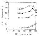
NiFeやFe等の磁性材料のエッチングにおいて、エッチング速度を保ちながらマスクとの選択比(磁性材料のエッチング速度/マスクのエッチング速度)を大きくすることは一般的に難しいとされているにもかかわらず、エッチングガスに一酸化炭素と含窒素化合物との混合ガスを用い、Tiをマスク材にすると特異的にTiのエッチング速度が遅く、大きな選択比をとることができる(図1)。
【0010】
本願発明者はこれについて研究を進めた結果、以下の二つの効果が相乗されてこのような結果がもたらされるものであることが分かった。
【0011】
第一の効果は、被エッチング材である磁性材料とTiのスパッタ率の差である。
【0012】
一般にCo、Fe、Niといった磁性を示す金属と比較してTiのスパッタ率は低いことが知られている。例えば、Arイオン500eVでのスパッタ率は、Coが1.2、Feが1.1又は0.84、Niが1.45又は1.33であるのに対し、Tiは、0.51と低い。
【0013】
すなわち、前述したようにスパッタリング作用が支配的になっていると考えられるドライエッチングにおいて、Tiが特異的に大きな選択比をとることができるのは、第一に、磁性を示す金属と比較してTiのスパッタ率が低いということによるものと考えられる。
【0014】
したがって、被エッチング材料が磁性材料である場合、前述したようにスパッタリング作用が支配的となるドライエッチングにおいて、高い選択比を確保するには、前記のTiのように被エッチング材料に比べてスパッタ率の小さい材料をマスク材としてまず採用することが重要である。
【0015】
磁性材料のエッチングにおいて、エッチングガスに一酸化炭素と含窒素化合物との混合ガスを用い、Tiをマスク材にすると、特異的にTiのエッチング速度が遅く、大きな選択比をとることができるという結果をもたらす第2の効果は、以下に説明するように、プラズマ化した一酸化炭素ガスと含窒素化合物ガスの混合ガスにより、マスク材のTiがより安定な状態に改質されることである。
【0016】
本願発明者が、Tiのエッチング速度が遅いことを更に調べたところ、図2図示のように、エッチングガスが、含窒素化合物のガス(NH3ガス、N2ガス)だけの場合よりも、一酸化炭素と含窒素化合物との混合ガスの場合の方が特にエッチング速度が遅く、大きな選択比がとれることが分かった。
【0017】
また、図1、図2に示された実験結果より、NH3ガスの流量比が大きくなるほど、つまり、一酸化炭素と含窒素化合物との混合ガスにおけるCOガスの流量比が小さくなるほど対Ti選択比が低下し(図1)、NH3ガスやN2ガスのみのように一酸化炭素(COガス)が全く入らない条件では対Ti選択比は低いことが分かった(図2)。
【0018】
すなわち、エッチングガスが、一酸化炭素と含窒素化合物との混合ガスの場合に、対Ti選択比が高い(大きい)のは、一酸化炭素(COガス)が多いほど、磁性材料であるNiFeと比較してTiのエッチング速度が低下しているためと考えられる。
【0019】
更に、本願発明者の実験によれば、あまりイオン入射エネルギーが違わない条件、例えば、図1の実験結果が得られた条件の下では、SiO2のエッチング速度は、NiFeやFeといった磁性膜と同じような挙動を示す。このことからも、一酸化炭素と含窒素化合物の混合ガスにおいて対Ti選択比が高くなるのは、磁性材料のエッチング速度が極めて高いからではなく、むしろTiのエッチング速度が一酸化炭素と含窒素化合物の混合ガスにおいて小さいためであるということが考えられる。
【0020】
そこで、発明者は、一酸化炭素と含窒素化合物との混合ガスの場合に、対Ti選択比が高く(大きく)なるのは、Ti表面の変質と考え、エッチングガスとして一酸化炭素と含窒素化合物との混合ガスを使用したドライエッチング処理後のTi膜の深さ方向のXPS(X−ray photoelectron spectroscopy)分析を行った。その結果、エッチング処理後のTi膜は、表面近傍数nm程度が高濃度に窒化し、また全体的に炭化していることが確認できた。
【0021】
すなわち、一酸化炭素と含窒素化合物との混合ガスをエッチングガスとして使用する場合にTi膜のエッチング速度が低下するのは、マスク材として用いられているTiの炭化と、窒化の2つが関与し、プラズマ状態にある一酸化炭素と含窒素化合物の混合ガスであるエッチングガスにより、マスク材であるTi膜が窒化物、あるいは炭化物となり、化学的にあるいは構造的により安定になることで、スパッタ率が更に減少したためであると考えられた。
【0022】
そこで、前記のTiのように被エッチング材料に比べてスパッタ率の小さい材料であることの他に、窒化物、又は炭化物を形成したときにより化学的、あるいは構造的な安定性を示す物性として、原子間のエネルギーに関係すると考えられる融点、あるいは沸点に注目し、周期律表のIV〜VI族の金属の中で、単体金属のときよりも窒化物あるいは炭化物に変化したときに、融点あるいは沸点が上昇する金属材料であることが高い選択比を持つためのもう一つの条件であると推測し、この発明を完成させた。
【0023】
【発明の実施の形態】
この発明が提案するドライエッチング用マスク材は、一酸化炭素と含窒素化合物の混合ガスをエッチングガスとして使用し磁性材料をドライエッチングする際のマスク用材料において、当該材料が窒化物あるいは炭化物に変化したときに融点又は沸点が上昇する金属からなることを特徴とするものである。
【0024】
前記における金属は、具体的には、タンタル(Ta)、タングステン(W)、ジルコニウム(Zr)、ハフニウム(Hf)のいずれかとすることができる。
【0025】
これらいずれの金属も、下記の表1の通り、磁性を示す金属と比較してスパッタ率が低く、かつ、単体金属より窒化物あるいは炭化物になったときに融点又は沸点が上昇するものであり、一酸化炭素と含窒素化合物の混合ガスをエッチングガスとして用いるドライエッチングにおいて、NiFeやCoFe等の磁性材料に対して高い選択比を示す傾向があり、磁性材料に対するドライエッチング用マスク材として良好である。
【0026】
【表1】
【0027】
前記の金属中、特に、Taは、以下の理由からTMR素子を構成する磁性材料に対するドライエッチング用マスク材として有効である。
【0028】
図3は、TMR用の磁性膜を構成するNiFe膜、CoFe膜のTaに対する選択比を測定したものであるが、CoFe膜のTaに対する選択比は10倍以上となっており、TaをNiFe膜、CoFe膜などの磁性材料をエッチングする際のマスク材として採用し得ることが確認できる。
【0029】
一方、TMR素子を構成する磁性薄膜は、素子として酸化による特性劣化を防ぎ化学的安定性等を確保するために、その表面に保護膜と呼ばれる導電性を有する非磁性の薄膜が形成されており、この保護膜には、通常Taが使用されている。Taが保護膜として使用される理由は、Taが保護膜としての安定性を有する他に、Ta膜を下地膜とした場合、その上に積層して形成されるNiFe等の、素子として重要な働きをする磁性膜が好ましいとされる配向面で成長するからである。
【0030】
そこで、この発明が提案するドライエッチング用マスク材としてTaを用いることにより、TMR素子の微細加工を行う過程において、TMR素子の保護膜として形成されるTaがマスクとして使用されているので、TMR素子の微細加工終了後にマスクを除去する必要がなくなり、これをそのまま残して保護膜として使用できる。
【0031】
すなわち、この発明が提案するドライエッチング用マスク材として良好な磁性膜形成に必要な下地膜でもあるTaを用いると、マスクに用いられたTaがTMR素子の構成要素(保護膜)となるので、エッチング終了後にマスクを除去する工程が不要になり、生産工程の短縮化、簡略化につながり、マスク用としてだけ別の材料を用意する必要がなくなり、設備、材料に関わるコストの削減を図ることができる。
【0032】
なお、前記において、反応性ガスとして用いる一酸化炭素と含窒素化合物の混合ガスにアルゴン(Ar)、ヘリウム(He)、キセノン(Xe)、クリプトン(Kr)、ネオン(Ne)等の第三のガスを添加ガスとして添加してもよい。これらの第三のガスを添加することにより、前述の一酸化炭素と含窒素化合物の混合ガスを希釈し、過度のガスの解離やエッチング生成物の再解離、再付着をコントロールすることができる。
【0033】
ただし、図4に示すように、一酸化炭素と含窒素化合物の混合ガスに対するArガスの添加量が大きいほど対Ti選択比は小さくなり、この傾向は、本発明において採用している単体金属より窒化物あるいは炭化物に変化したときに融点又は沸点が上昇する金属(Ta、W、Zr、Hf)においても示されるので、Arガスのような前述した第三のガスを一酸化炭素と含窒素化合物の混合ガスに添加する場合、その添加量は80%以下とすることが望ましい。
【0034】
【実験例】
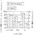
一酸化炭素と含窒素化合物の混合ガスをエッチングガスとして使用し磁性材料をドライエッチングする際のマスク用材料として本発明が提案するタンタル(Ta)を採用した場合について、TMR素子に対して、図5に示すようなヘリコン波プラズマ源搭載のエッチング装置を用いてエッチングを行った。
【0035】
図6にTMR素子の基本的な構造を示す。
【0036】
TMR素子を特徴付けるTMR構造は、膜厚が1nmの絶縁層であるAl2O3膜を挟んで、ピン層(Al2O3の上層)とフリー層(Al2O3の下層)と呼ばれる2つのCoFeからなる強磁性層(膜厚は、ピン層が5nm、フリー層が10nm)と、ピン層の上層で反強磁性層のFeMn(膜厚20nm)からなる。なお、ここでは、TMR素子の基本原理、動作の説明は省略する。
【0037】
更に、生産工程中、大気と接する最上層には、TMR素子の保護層であり、かつ、絶縁層であるAl2O3を含めた磁性層のドライエッチング用のマスクでもあるTaが積層している。Taは、ドライエッチング後、保護層としての膜厚を確保させるため、エッチング前は9nmの膜厚に積層される。保護層(Ta)、反強磁性層(FeMn)、強磁性層(CoFe)、絶縁層(Al2O3)は、一般的にはスパッタリングで順次形成される。
【0038】
まず、図6(a)図示の構成のTMR素子に対して、SF6ガスを用いて、PRをマスクとして、Ta膜をエッチングし、図6(b)図示のように形成されたTa膜を絶縁層であるAl2O3を含めた磁性層(FeMn、CoFe)のマスクとした。このプロセスは以下のように行った。
【0039】
図5図示の真空容器2内を排気系21によって排気し、不図示のゲートバルブを開けて図6(a)図示の構成のTMR素子となるTMR膜を積層したウェーハ9を真空容器2内に搬入し、対象物ホルダー4に保持し、温度制御機構41により所定温度に維持した。次に、ガス導入系3を動作させ、図5には不図示のSF6ガスを溜めているボンベから不図示の配管、バルブ、流量調整器を介して、所定の流量のエッチングガス(SF6)を真空容器2内へ導入する。導入されたエッチングガスは、真空容器2内を経由して誘電体壁容器11内に拡散する。ここで、プラズマ源1を動作させる。プラズマ源1は、真空容器2に対して内部空間が連通するようにして気密に接続された誘電体壁容器11と、誘電体壁容器11内にヘリコン波を誘起する2ターンのアンテナ12と、アンテナ12に不図示の整合器を介して伝送路15によって接続され、アンテナ12に供給する高周波電力(ソース電力)を発生させるプラズマ用高周波電源13と、誘電体壁容器11内に所定の磁界を生じさせる電磁石14等とから構成されている。プラズマ用高周波電源13が発生させた高周波が伝送路15によってアンテナ12に供給された際に、2ターンのアンテナ12に互いに逆向きの電流が流れ、この結果、誘電体壁容器11の内部にヘリコン波が誘起される。このヘリコン波のエネルギーがエッチングガスに与えられてヘリコン波プラズマが形成される。なお、真空容器2の側壁の外側には、多数の側壁用磁石22が、真空容器2の側壁を臨む面の磁極が隣り合う磁石同士で互いに異なるように周方向に多数並べて配置され、これによってカスプ磁場が真空容器2の側壁の内面に沿って周方向に連なって形成され、真空容器2の側壁の内面へのプラズマの拡散が防止されている。この時、同時に、バイアス用高周波電源5を作動させて、エッチング処理対象物であるウェーハ9に負の直流分の電圧であるセルフバイアス電圧が与えられ、プラズマからウェーハ9の表面へのイオン入射エネルギーを制御している。前記のようにして形成されたプラズマが誘電体壁容器11から真空容器2内に拡散し、ウェーハ9の表面付近にまで達する。この際、ウェーハ9の表面がエッチングされる。
【0040】
なお、以上のSF6を用いたPRマスクによるTa膜のエッチングプロセスは、エッチングガス(SF6)の流量:326mg/min.(50sccm)、ソース電力:1000W、バイアス電力:100W、真空容器2内の圧力:0.5Pa、ウェーハ9の温度:50℃で行った。
【0041】
次に、COガスとNH3ガスとの混合ガスをエッチングガスとして用いて、前記のプロセスによって形成されたTaマスクで磁性膜をエッチングした。
【0042】
このプロセスも、図5図示のヘリコン波プラズマ源搭載のエッチング装置を用いて行うものであるが、前記のプロセスにおいて、図示しないガス導入系を動作させてSF6ガスをエッチングガスとして真空容器2内へ導入したプロセスを、ガス導入系3を動作させて、図5図示のCOガスを溜めているボンベ31a及びNH3ガスを溜めているボンベ31bから、配管32、バルブ33、流量調整器34を介して、所定の混合比及び流量のエッチングガス(COガス及びNH3ガスの混合ガス)を真空容器2内へ導入するプロセスに変更し、他は、前述のプロセスと同様にエッチングを行い、図6(c)図示のTMR素子を得た。
【0043】
このTa膜マスクによる磁性膜のエッチングプロセスは、エッチングガスの流量:COガス:12.5mg/min.(10sccm)、NH3ガス:22.8mg/min.(30sccm)、ソース電力:3000W、バイアス電力:1200W、真空容器2内の圧力:0.8Pa、ウェーハ9の温度:100℃で行ったものである。
【0044】
以上のプロセスにてTMR素子をエッチングしたところ、パターン側壁への付着膜は発生しなかった。
【0045】
一方、TMR素子をArガスを用いてPRマスクでエッチングしたところ、パターン側壁に付着膜が生じていた。
【0046】
この結果、図3に示すように、一酸化炭素と含窒素化合物の混合ガスをエッチングガスとして使用し、TMR素子を構成する磁性材料をドライエッチングする際のマスク用材料としてTiと同等以上のエッチング性能(CoFeエッチング速度:63.1nm/min.、Taエッチング速度:5.7nm/min.、選択比(対CoFe):11)が得られ、エッチング後、膜厚5nmの保護膜としてTa膜をそのまま残した。
【0047】
更に、Taをマスク材として用いると、ドライエッチングにより発生する反応生成物に起因するパターン側壁への付着物が低減されるため、テーパー角も大きく、パターン側壁への付着物の少ないエッチングを行えることが示された。
【0048】
以上、この発明の好ましい実施の形態、実験例を説明したが、本発明は、前述した実施の形態に限定されるものではなく、特許請求の範囲の記載から把握される技術的範囲において、種々の形態に変更可能である。
【0049】
例えば、一酸化炭素と含窒素化合物の混合ガスをエッチングガスとし、本発明が提案するTa等の金属を、TMR素子を構成する磁性薄膜のドライエッチング用のマスク材として用いる場合、TMR素子の構成は、図6図示の構成に限定されるものではない。
【0050】
また、前記実験例では、エッチング装置としてヘリコン波プラズマ源搭載のエッチング装置を用いたが、エッチング装置はこれに限られるものではなく、平行平板型RIE、マグネトロンRIE、ECR、ICPなどを用いることができる。
【0051】
【発明の効果】
この発明によれば、TMR膜を構成するNiFeやCoFeのように数nm程度の薄い磁性膜の微細加工に適したドライエッチング用のマスク材、更に、このようなマスク材であって、なおかつ、TMR素子の生産工程の簡略化、設備、材料に関わる製造コストの低減を図ることのできるドライエッチング用のマスク材を提供することができる。
【図面の簡単な説明】
【図1】一酸化炭素と含窒素化合物の混合ガスにおけるエッチング速度の実験結果を表すグラフ。
【図2】NiFeエッチング速度と対Ti選択比の反応性ガスによる相違を表すグラフ。
【図3】TMR素子用磁性膜のCO/NH3エッチング特性を表すグラフ。
【図4】エッチング速度と対Ti選択比のArガス添加量依存度を表すグラフ。
【図5】本発明のTaマスクでCO+NH3ガスを用いて磁性膜のエッチングを行う際に使用できるエッチング装置の概略構成図。
【図6】本発明のTaマスクを用いてTMR素子のエッチングを行う際のプロセスを表す図であって、
(a)は、プロセス開始前の断面概略図、
(b)は、PRをマスクとしてTa膜をエッチングした状態の断面概略図、
(c)は、Taマスクで、磁性膜をエッチングした状態の断面概略図。
【符号の説明】
1 プラズマ源
2 真空容器
3 ガス導入系
4 対象物ホルダー
5 バイアス用高周波電源
9 ウェーハ
11 誘電体壁容器
12 アンテナ
13 プラズマ用高周波電源
14 電磁石
15 伝送路
21 排気系
22 側壁用磁石
31a、31b ボンベ
32 配管
33 バルブ
34 流量調整器
41 温度制御機構[0001]
BACKGROUND OF THE INVENTION
The present invention relates to an etching mask material used in a process of etching a magnetic material such as Ni, Fe, Co, and more particularly, a magnetic head used for writing to a magnetic disk, an integrated magnetic memory, etc. New mask material for dry etching useful for manufacturing, especially mask material used for fine processing by dry etching of magnetic multilayer thin film constituting magnetoresistive elements such as GMR (giant magnetoresistance) and TMR (tunneling magnetoresistance) About.
[0002]
[Prior art]
MRAM (magnetic random access memory), which is an integrated magnetic memory that is attracting attention as an unlimitedly rewritable memory, has an integration density similar to that of a DRAM and has a high speed equivalent to that of an SRAM. A TMR (tunneling magnetoresistive) film composed of a nonmagnetic or magnetic thin film is used.
[0003]
There have been few proposals for a mask material for dry etching suitable for fine processing of a magnetic film as thin as several nanometers such as NiFe and CoFe constituting the TMR film.
[0004]
As a mask for dry etching, Japanese Patent Application Laid-Open No. 11-92971 discloses a reactive ion etching mask by plasma using a mixed gas of carbon monoxide and a nitrogen-containing compound, such as titanium, magnesium, aluminum, germanium, platinum, There has been proposed a mask composed of at least one of palladium and each of these or an alloy or compound containing two or more of them as a main component. However, Japanese Patent Application Laid-Open No. 11-92971 does not mention an important selection ratio as etching characteristics, and has not studied an optimal mask material in view of the entire production process of TMR elements and the like. .
[0005]
[Problems to be solved by the invention]
The present invention relates to a mask material for dry etching suitable for microfabrication of a thin magnetic film of about several nanometers such as NiFe and CoFe constituting a TMR film, and further to such a mask material, further comprising a TMR element An object of the present invention is to propose a mask material for dry etching that can simplify the production process and reduce the manufacturing cost related to equipment and materials.
[0006]
[Means for Solving the Problems]
One method of dry etching called RIE (reactive ion etching), which is widely used today as a means of microfabrication in semiconductor manufacturing processes, is to place a workpiece in an etching gas plasma and apply an electric field, A chemical action and a physical action are caused simultaneously to etch only a specific substance.
[0007]
In principle, the chemical action of ions, radicals, etc. of the etching gas generated in the plasma by the physical action of sputtering and evaporation caused by ions perpendicularly incident on the surface of the workpiece not covered by the mask Highly volatile products generated by the chemical action that the active species collide or adsorb on the surface of the workpiece, cause a chemical reaction with the workpiece, and form a surface reaction layer with low binding energy. It is thought that it is progressing by desorption.
[0008]
The inventor of the present application has advanced research using Ti, which is proposed as the most desirable substance in the above-mentioned JP-A-11-92971, and it is considered that the dry etching of the present invention is proceeding mainly by sputtering. I found out.
[0009]
In the etching of magnetic materials such as NiFe and Fe, it is generally difficult to increase the selection ratio with the mask (magnetic material etching rate / mask etching rate) while maintaining the etching rate. When a mixed gas of carbon monoxide and a nitrogen-containing compound is used as an etching gas and Ti is used as a mask material, the etching rate of Ti is specifically slow, and a large selection ratio can be obtained (FIG. 1).
[0010]
The inventor of the present application conducted research on this, and as a result, found that the following two effects were synergistic and brought about such a result.
[0011]
The first effect is a difference in sputtering rate between the magnetic material to be etched and Ti.
[0012]
In general, it is known that the sputtering rate of Ti is low as compared with metals exhibiting magnetism such as Co, Fe, and Ni. For example, the sputtering rate at Ar ions of 500 eV is 1.2 for Co, 1.1 or 0.84 for Fe, and 1.45 or 1.33 for Ni, whereas Ti is as low as 0.51. .
[0013]
That is, as described above, in dry etching, in which the sputtering action is considered to be dominant, Ti can take a specifically large selection ratio compared to a metal exhibiting magnetism. This is thought to be due to the low sputtering rate of Ti.
[0014]
Therefore, when the material to be etched is a magnetic material, the sputtering rate is higher than that of the material to be etched, such as Ti, in order to ensure a high selectivity in the dry etching in which the sputtering action is dominant as described above. It is important to first adopt a material having a small thickness as a mask material.
[0015]
When etching a magnetic material, using a mixed gas of carbon monoxide and a nitrogen-containing compound as an etching gas and using Ti as a mask material results in that the etching rate of Ti is specifically slow and a large selectivity can be obtained. As described below, the second effect is that the Ti of the mask material is modified to a more stable state by the mixed gas of plasma carbon monoxide gas and nitrogen-containing compound gas.
[0016]
The inventor of the present application further investigated that the etching rate of Ti is slow, and as shown in FIG. 2, the etching gas is one more than the case where the etching gas is only a nitrogen-containing compound gas (NH3 gas, N2 gas). It was found that the etching rate was particularly slow in the case of a mixed gas of carbon oxide and nitrogen-containing compound, and a large selectivity could be obtained.
[0017]
Further, from the experimental results shown in FIGS. 1 and 2, the larger the NH3 gas flow ratio, that is, the smaller the CO gas flow ratio in the mixed gas of carbon monoxide and nitrogen-containing compound, the smaller the Ti selection. The ratio decreased (FIG. 1), and it was found that the ratio of Ti to Ti was low (FIG. 2) under the condition that no carbon monoxide (CO gas) entered, such as NH3 gas or N2 gas alone.
[0018]
That is, when the etching gas is a mixed gas of carbon monoxide and a nitrogen-containing compound, the selectivity to Ti is high (large) because the more carbon monoxide (CO gas) is, the more NiFe that is a magnetic material is. This is probably because the etching rate of Ti is decreased.
[0019]
Furthermore, according to the experiment by the present inventor, the etching rate of SiO2 is different from that of a magnetic film such as NiFe or Fe under conditions where the ion incident energy is not so different, for example, under the condition where the experimental result of FIG. 1 is obtained. Shows similar behavior. Also from this, the selective ratio to Ti in the mixed gas of carbon monoxide and nitrogen-containing compound is not because the etching rate of the magnetic material is very high, but rather the etching rate of Ti is carbon monoxide and nitrogen-containing. It is conceivable that this is because the mixed gas of the compound is small.
[0020]
In view of this, the inventor considered that a high (large) ratio of Ti to Ti in the case of a mixed gas of carbon monoxide and a nitrogen-containing compound is an alteration of the Ti surface, and carbon monoxide and nitrogen-containing etching gas. XPS (X-ray photoelectron spectroscopy) analysis in the depth direction of the Ti film after dry etching using a mixed gas with a compound was performed. As a result, it was confirmed that the Ti film after the etching treatment was nitrided at a high concentration in the vicinity of the surface several nanometers and carbonized as a whole.
[0021]
That is, when a mixed gas of carbon monoxide and a nitrogen-containing compound is used as an etching gas, the etching rate of the Ti film is decreased due to two factors, namely, carbonization of Ti used as a mask material and nitriding. The etching rate, which is a mixed gas of carbon monoxide and nitrogen-containing compound in the plasma state, turns the Ti film, which is a mask material, into nitrides or carbides, which are chemically or structurally more stable, thereby increasing the sputtering rate. This was thought to be due to a further decrease.
[0022]
Therefore, in addition to being a material having a smaller sputtering rate than the material to be etched, such as Ti described above, as a physical property showing more chemical or structural stability when nitride or carbide is formed, Paying attention to the melting point or boiling point that is considered to be related to the energy between atoms, the melting point or boiling point when changing to a nitride or carbide in the IV-VI group metals of the periodic table rather than a single metal It is presumed that the metal material that rises is another condition for having a high selection ratio, and the present invention has been completed.
[0023]
DETAILED DESCRIPTION OF THE INVENTION
The mask material for dry etching proposed by the present invention is a mask material used when dry etching a magnetic material using a mixed gas of carbon monoxide and a nitrogen-containing compound as an etching gas, and the material is changed to nitride or carbide. It is characterized by being made of a metal whose melting point or boiling point rises.
[0024]
Specifically, the metal in the above can be any one of tantalum (Ta), tungsten (W), zirconium (Zr), and hafnium (Hf).
[0025]
Each of these metals has a low sputtering rate as compared with metals exhibiting magnetism as shown in Table 1 below, and its melting point or boiling point rises when it becomes a nitride or carbide from a single metal, In dry etching using a mixed gas of carbon monoxide and a nitrogen-containing compound as an etching gas, there is a tendency to show a high selection ratio with respect to magnetic materials such as NiFe and CoFe, which is favorable as a mask material for dry etching with respect to magnetic materials. .
[0026]
[Table 1]
[0027]
Of these metals, Ta is particularly effective as a dry etching mask material for the magnetic material constituting the TMR element for the following reasons.
[0028]
FIG. 3 shows the measurement of the selectivity ratio of the NiFe film and the CoFe film constituting the magnetic film for TMR to Ta. The selectivity ratio of the CoFe film to Ta is 10 times or more. It can be confirmed that it can be used as a mask material when etching a magnetic material such as a CoFe film.
[0029]
On the other hand, the magnetic thin film constituting the TMR element has a non-magnetic thin film having conductivity called a protective film formed on its surface in order to prevent deterioration of characteristics due to oxidation and to ensure chemical stability. In this protective film, Ta is usually used. The reason why Ta is used as a protective film is that, in addition to the stability of Ta as a protective film, when a Ta film is used as a base film, it is important as an element such as NiFe formed by being laminated thereon. This is because a magnetic film that works is grown on an orientation plane that is considered preferable.
[0030]
Therefore, by using Ta as a mask material for dry etching proposed by the present invention, Ta formed as a protective film of the TMR element is used as a mask in the process of fine processing of the TMR element. Therefore, it is not necessary to remove the mask after finishing the microfabrication, and the mask can be left as it is and used as a protective film.
[0031]
That is, when Ta, which is a base film necessary for forming a good magnetic film, is used as a mask material for dry etching proposed by the present invention, Ta used for the mask becomes a component (protective film) of the TMR element. The process of removing the mask after etching is no longer necessary, leading to shortening and simplification of the production process, eliminating the need to prepare a separate material only for the mask, and reducing costs related to equipment and materials. it can.
[0032]
In the above, a mixed gas of carbon monoxide and nitrogen-containing compound used as a reactive gas is a third gas such as argon (Ar), helium (He), xenon (Xe), krypton (Kr), neon (Ne), etc. A gas may be added as an additive gas. By adding these third gases, the above-mentioned mixed gas of carbon monoxide and nitrogen-containing compound can be diluted, and excessive gas dissociation and re-dissociation and reattachment of etching products can be controlled.
[0033]
However, as shown in FIG. 4, the larger the amount of Ar gas added to the mixed gas of carbon monoxide and nitrogen-containing compound, the smaller the selectivity with respect to Ti becomes. This tendency is higher than that of the single metal employed in the present invention. Since it is also shown in metals (Ta, W, Zr, Hf) whose melting point or boiling point rises when changing to nitride or carbide, the aforementioned third gas such as Ar gas is replaced with carbon monoxide and nitrogen-containing compounds. When added to the mixed gas, the added amount is desirably 80% or less.
[0034]
[Experimental example]
In the case where tantalum (Ta) proposed by the present invention is used as a mask material when dry etching a magnetic material using a mixed gas of carbon monoxide and a nitrogen-containing compound as an etching gas, Etching was performed using an etching apparatus equipped with a helicon wave plasma source as shown in FIG.
[0035]
FIG. 6 shows a basic structure of the TMR element.
[0036]
The TMR structure that characterizes the TMR element is called a pinned layer (upper layer of Al2 O3 ) and a free layer (lower layer of Al2 O3 ) with an Al2 O3 film that is an insulating layer having a thickness of 1 nm interposed therebetween 2 One CoFe ferromagnetic layer (the film thickness is 5 nm for the pinned layer and 10 nm for the free layer) and the upper layer of the pinned layer is FeMn (film thickness is 20 nm). Here, the description of the basic principle and operation of the TMR element is omitted.
[0037]
Further, during the production process, Ta, which is a protective layer for the TMR element and a mask for dry etching of the magnetic layer including Al2 O3 which is an insulating layer, is laminated on the uppermost layer in contact with the atmosphere. Yes. Ta is laminated to a thickness of 9 nm before etching in order to ensure a film thickness as a protective layer after dry etching. The protective layer (Ta), antiferromagnetic layer (FeMn), ferromagnetic layer (CoFe), and insulating layer (Al2 O3 ) are generally formed sequentially by sputtering.
[0038]
First, the Ta film is etched with respect to the TMR element having the configuration shown in FIG. 6A using SF6 gas using PR as a mask, and the Ta film formed as shown in FIG. A mask of a magnetic layer (FeMn, CoFe) including Al2 O3 as an insulating layer was used. This process was performed as follows.
[0039]
The
[0040]
Note that the etching process of the Ta film with the PR mask using SF6 described above is performed by using an etching gas (SF6 ) flow rate of 326 mg / min. (50 sccm), source power: 1000 W, bias power: 100 W, pressure in vacuum vessel 2: 0.5 Pa, temperature of wafer 9: 50 ° C.
[0041]
Next, the magnetic film was etched with the Ta mask formed by the above process using a mixed gas of CO gas and NH3 gas as an etching gas.
[0042]
This process is also performed using the etching apparatus equipped with the helicon wave plasma source shown in FIG. 5. In the above process, a gas introduction system (not shown) is operated to use SF6 gas as an etching gas in the
[0043]
The etching process of the magnetic film using the Ta film mask is performed by using an etching gas flow rate: CO gas: 12.5 mg / min. (10 sccm), NH3 gas: 22.8 mg / min. (30 sccm), source power: 3000 W, bias power: 1200 W, pressure in vacuum vessel 2: 0.8 Pa, temperature of wafer 9: 100 ° C.
[0044]
When the TMR element was etched by the above process, an adhesion film on the pattern side wall was not generated.
[0045]
On the other hand, when the TMR element was etched with a PR mask using Ar gas, an adhesion film was formed on the pattern side wall.
[0046]
As a result, as shown in FIG. 3, a mixed gas of carbon monoxide and a nitrogen-containing compound is used as an etching gas, and etching that is equal to or more than Ti is used as a mask material when dry-etching the magnetic material constituting the TMR element. Performance (CoFe etching rate: 63.1 nm / min., Ta etching rate: 5.7 nm / min., Selectivity (vs. CoFe): 11) is obtained, and after etching, a Ta film is used as a protective film having a thickness of 5 nm. I left it as it was.
[0047]
Furthermore, when Ta is used as a mask material, the deposit on the pattern side wall due to the reaction product generated by dry etching is reduced, so that the taper angle is large and etching with a small amount of deposit on the pattern side wall can be performed. It has been shown.
[0048]
As mentioned above, although preferable embodiment and experiment example of this invention were described, this invention is not limited to embodiment mentioned above, In the technical range grasped | ascertained from description of a claim, various It is possible to change to the form.
[0049]
For example, when a mixed gas of carbon monoxide and a nitrogen-containing compound is used as an etching gas and a metal such as Ta proposed by the present invention is used as a mask material for dry etching of a magnetic thin film constituting a TMR element, the structure of the TMR element is used. Is not limited to the configuration shown in FIG.
[0050]
In the experimental example, an etching apparatus equipped with a helicon wave plasma source is used as the etching apparatus. However, the etching apparatus is not limited to this, and parallel plate RIE, magnetron RIE, ECR, ICP, or the like may be used. it can.
[0051]
【The invention's effect】
According to this invention, a mask material for dry etching suitable for microfabrication of a thin magnetic film of about several nanometers such as NiFe and CoFe constituting the TMR film, and further, such a mask material, It is possible to provide a mask material for dry etching capable of simplifying the production process of the TMR element and reducing the manufacturing cost related to equipment and materials.
[Brief description of the drawings]
FIG. 1 is a graph showing experimental results of etching rate in a mixed gas of carbon monoxide and a nitrogen-containing compound.
FIG. 2 is a graph showing the difference between NiFe etching rate and Ti selectivity with reactive gas.
FIG. 3 is a graph showing CO / NH3 etching characteristics of a magnetic film for a TMR element.
FIG. 4 is a graph showing the dependence of the etching rate and the Ti selectivity on the Ar gas addition amount.
FIG. 5 is a schematic configuration diagram of an etching apparatus that can be used when etching a magnetic film using CO + NH3 gas with the Ta mask of the present invention.
FIG. 6 is a diagram showing a process for etching a TMR element using the Ta mask of the present invention,
(A) is a schematic cross-sectional view before starting the process,
(B) is a schematic cross-sectional view of a state in which the Ta film is etched using PR as a mask;
(C) is a schematic cross-sectional view of a state in which the magnetic film is etched with a Ta mask.
[Explanation of symbols]
DESCRIPTION OF
Claims (1)
Translated fromJapanese窒化物あるいは炭化物に変化したときに融点又は沸点が上昇する金属であるタンタルの金属からなるマスクで、前記TMR構造体を形成するための積層体をマスクする工程、そして
一酸化炭素と含窒素化合物の混合ガスをエッチングガスとして使用して前記マスクされた前記積層体をドライエッチングしてTMR構造体を形成する工程とからなり、
前記TMR構造体上層の保護膜をドライエッチング工程後の前記タンタルマスクで構成しているTMR磁性素子の製造方法。In a method for manufacturing a TMR magnetic element having a TMR structure including a pinned layer that is an upper layer of the insulating layer and a ferromagnetic layer that is a free layer that is a lower layer of the insulating layer with the insulating layer interposed therebetween,
The mask having a melting point or boiling point is made of a metal derRu tantalum metal which rises when changes to the nitride or carbide, a step of masking thelaminate for forming the TMR structureand carbon monoxide andnitrogen-containing,Forming aTMR structure by dry-etching the maskedlaminate using a compound gas as an etching gas,
A method for manufacturing a TMR magnetic element, wherein the protective film on the TMR structure upper layer is constituted by the tantalum mask after a dry etching process.
Priority Applications (5)
| Application Number | Priority Date | Filing Date | Title |
|---|---|---|---|
| JP2000224248AJP4605554B2 (en) | 2000-07-25 | 2000-07-25 | Mask material for dry etching |
| US09/910,854US20020038681A1 (en) | 2000-07-25 | 2001-07-24 | Masking material for dry etching |
| KR1020010044924AKR100955000B1 (en) | 2000-07-25 | 2001-07-25 | Manufacturing method of magnetic element |
| US11/601,737US20070119811A1 (en) | 2000-07-25 | 2006-11-20 | Masking material for dry etching |
| US12/219,117US8524094B2 (en) | 2000-07-25 | 2008-07-16 | Masking material for dry etching |
Applications Claiming Priority (1)
| Application Number | Priority Date | Filing Date | Title |
|---|---|---|---|
| JP2000224248AJP4605554B2 (en) | 2000-07-25 | 2000-07-25 | Mask material for dry etching |
Publications (2)
| Publication Number | Publication Date |
|---|---|
| JP2002038285A JP2002038285A (en) | 2002-02-06 |
| JP4605554B2true JP4605554B2 (en) | 2011-01-05 |
Family
ID=18718240
Family Applications (1)
| Application Number | Title | Priority Date | Filing Date |
|---|---|---|---|
| JP2000224248AExpired - LifetimeJP4605554B2 (en) | 2000-07-25 | 2000-07-25 | Mask material for dry etching |
Country Status (3)
| Country | Link |
|---|---|
| US (3) | US20020038681A1 (en) |
| JP (1) | JP4605554B2 (en) |
| KR (1) | KR100955000B1 (en) |
Families Citing this family (20)
| Publication number | Priority date | Publication date | Assignee | Title |
|---|---|---|---|---|
| JP4594235B2 (en)* | 2002-12-23 | 2010-12-08 | 東京エレクトロン株式会社 | Method for etching an ARC layer |
| JP2004269910A (en)* | 2003-03-05 | 2004-09-30 | Tdk Corp | Magnetic material dry etching method, magnetic material, and magnetic recording medium |
| JP4170165B2 (en)* | 2003-06-30 | 2008-10-22 | Tdk株式会社 | Mask material for reactive ion etching, mask and dry etching method |
| JP2006060044A (en) | 2004-08-20 | 2006-03-02 | Canon Anelva Corp | Method for manufacturing magnetoresistive element |
| RU2008140382A (en)* | 2006-03-16 | 2010-04-27 | Новартис АГ (CH) | HETEROCYCLIC ORGANIC COMPOUNDS, FOR example, FOR THE TREATMENT OF MELANOMA |
| KR20090020150A (en) | 2007-08-22 | 2009-02-26 | 삼성전자주식회사 | Adaptive Unified IP Message Service Terminal and Message Sending and Receiving Method |
| US20090078674A1 (en)* | 2007-09-26 | 2009-03-26 | Silverbrook Research Pty Ltd | Reactive Ion Etching Process for Etching Metals |
| WO2009084445A1 (en)* | 2007-12-27 | 2009-07-09 | Canon Anelva Corporation | Dry etching method, magnetoresistive element, and method and apparatus for manufacturing the same |
| WO2009096328A1 (en) | 2008-01-29 | 2009-08-06 | Ulvac, Inc. | Magnetic device manufacturing method |
| US8158445B2 (en) | 2009-11-11 | 2012-04-17 | Samsung Electronics Co., Ltd. | Methods of forming pattern structures and methods of manufacturing semiconductor devices using the same |
| US8334148B2 (en) | 2009-11-11 | 2012-12-18 | Samsung Electronics Co., Ltd. | Methods of forming pattern structures |
| JP2010045398A (en)* | 2009-11-17 | 2010-02-25 | Canon Anelva Corp | Method for manufacturing magnetoresistance effect element |
| US8546263B2 (en)* | 2011-04-27 | 2013-10-01 | Applied Materials, Inc. | Method of patterning of magnetic tunnel junctions |
| CN102931143B (en)* | 2011-08-10 | 2015-04-29 | 无锡华润上华科技有限公司 | Method for manufacturing NOR flash device |
| KR101578178B1 (en)* | 2011-10-31 | 2015-12-16 | 캐논 아네르바 가부시키가이샤 | Ion beam etching method for magnetic films and ion beam etching apparatus |
| JP5883772B2 (en)* | 2012-11-27 | 2016-03-15 | 株式会社日立ハイテクノロジーズ | Plasma processing method |
| JP5919183B2 (en) | 2012-12-17 | 2016-05-18 | 株式会社日立ハイテクノロジーズ | Plasma etching method |
| JP2018098287A (en) | 2016-12-09 | 2018-06-21 | 東芝メモリ株式会社 | Manufacturing method of semiconductor device |
| JP6878154B2 (en)* | 2017-06-05 | 2021-05-26 | 東京エレクトロン株式会社 | Etching method and etching equipment |
| US10859644B2 (en) | 2019-03-20 | 2020-12-08 | Nxp B.V. | Manufacturing of high performance magnetoresistive sensors |
Family Cites Families (23)
| Publication number | Priority date | Publication date | Assignee | Title |
|---|---|---|---|---|
| US3642548A (en)* | 1969-08-20 | 1972-02-15 | Siemens Ag | Method of producing integrated circuits |
| JPS5593225A (en)* | 1979-01-10 | 1980-07-15 | Hitachi Ltd | Forming method of minute pattern |
| US5607599A (en)* | 1994-11-17 | 1997-03-04 | Kabushiki Kaisha Toshiba | Method of processing a magnetic thin film |
| WO1996019800A1 (en)* | 1994-12-20 | 1996-06-27 | Citizen Watch Co., Ltd. | Method of processing magnetic head slider |
| JP2677321B2 (en)* | 1995-03-15 | 1997-11-17 | 科学技術庁金属材料技術研究所長 | Dry etching method |
| GB9520901D0 (en)* | 1995-10-12 | 1995-12-13 | Philips Electronics Nv | Electronic device manufacture |
| GB9521855D0 (en)* | 1995-10-25 | 1996-01-03 | Philips Electronics Nv | Manufacture of electronic devices comprising thin-film circuitry |
| KR100413649B1 (en)* | 1996-01-26 | 2004-04-28 | 마츠시타 덴끼 산교 가부시키가이샤 | Method of manufacturing semiconductor devices |
| US5946167A (en)* | 1996-03-15 | 1999-08-31 | Kabushiki Kaisha Toshiba | Magnetoresistive sensor having lead and/or bias layer structure contributing to a narrow gap |
| US6090697A (en)* | 1997-06-30 | 2000-07-18 | Texas Instruments Incorporated | Etchstop for integrated circuits |
| DE19728472A1 (en)* | 1997-07-03 | 1999-01-07 | Siemens Ag | Structuring process |
| US6391216B1 (en)* | 1997-09-22 | 2002-05-21 | National Research Institute For Metals | Method for reactive ion etching and apparatus therefor |
| JP3131595B2 (en)* | 1997-09-22 | 2001-02-05 | 科学技術庁金属材料技術研究所長 | Mask for reactive ion etching |
| US5985104A (en)* | 1997-10-09 | 1999-11-16 | International Business Machines Corporation | Sputtered mask defined with highly selective side wall chemical etching |
| US6046109A (en)* | 1997-12-29 | 2000-04-04 | Industrial Technology Research Institute | Creation of local semi-insulating regions on semiconductor substrates |
| US5994235A (en)* | 1998-06-24 | 1999-11-30 | Lam Research Corporation | Methods for etching an aluminum-containing layer |
| JP4104748B2 (en)* | 1998-10-12 | 2008-06-18 | 富士通株式会社 | Magnetic sensor, magnetic head and magnetic encoder |
| FR2786279B1 (en)* | 1998-11-24 | 2000-12-29 | Cit Alcatel | OPTICAL COMPONENT BASED ON SEMICONDUCTOR OPTICAL AMPLIFIERS WITH A REDUCED NUMBER OF INDEPENDENT ELECTRODES |
| US6194323B1 (en)* | 1998-12-16 | 2001-02-27 | Lucent Technologies Inc. | Deep sub-micron metal etch with in-situ hard mask etch |
| JP3537337B2 (en)* | 1998-12-28 | 2004-06-14 | 株式会社東芝 | Method of manufacturing thin film device, magnetoresistive head manufactured by this method, and magnetic recording / reproducing apparatus equipped with this head |
| US6602620B1 (en)* | 1998-12-28 | 2003-08-05 | Kabushiki Kaisha Toshiba | Magnetic recording apparatus, magnetic recording medium and manufacturing method thereof |
| JP3959881B2 (en)* | 1999-02-08 | 2007-08-15 | Tdk株式会社 | Method for manufacturing magnetoresistive sensor |
| JP3433721B2 (en)* | 2000-03-28 | 2003-08-04 | ティーディーケイ株式会社 | Dry etching method and fine processing method |
- 2000
- 2000-07-25JPJP2000224248Apatent/JP4605554B2/ennot_activeExpired - Lifetime
- 2001
- 2001-07-24USUS09/910,854patent/US20020038681A1/ennot_activeAbandoned
- 2001-07-25KRKR1020010044924Apatent/KR100955000B1/ennot_activeExpired - Fee Related
- 2006
- 2006-11-20USUS11/601,737patent/US20070119811A1/ennot_activeAbandoned
- 2008
- 2008-07-16USUS12/219,117patent/US8524094B2/ennot_activeExpired - Fee Related
Also Published As
| Publication number | Publication date |
|---|---|
| KR100955000B1 (en) | 2010-04-27 |
| US20070119811A1 (en) | 2007-05-31 |
| US20020038681A1 (en) | 2002-04-04 |
| JP2002038285A (en) | 2002-02-06 |
| US20080277377A1 (en) | 2008-11-13 |
| US8524094B2 (en) | 2013-09-03 |
| KR20020009517A (en) | 2002-02-01 |
Similar Documents
| Publication | Publication Date | Title |
|---|---|---|
| JP4605554B2 (en) | Mask material for dry etching | |
| JP4111274B2 (en) | Magnetic material dry etching method | |
| KR101066158B1 (en) | Manufacturing method and apparatus of magnetic element | |
| US9601688B2 (en) | Method of manufacturing magnetoresistive element and method of processing magnetoresistive film | |
| JP2009278130A (en) | Method for producing magnetoresistive element | |
| TWI629724B (en) | Etching method of etched layer | |
| TW201503257A (en) | Plasma etching method | |
| WO2009110469A1 (en) | Method for manufacturing magnetic tunnel junction device and apparatus for manufacturing magnetic tunnel junction device | |
| WO2010084909A1 (en) | Method for cleaning magnetic film processing chamber, method for manufacturing magnetic element, and substrate processing apparatus | |
| JP6018220B2 (en) | Method for manufacturing magnetoresistive element | |
| KR102365473B1 (en) | Method for etching object to be processed | |
| JP4364669B2 (en) | Dry etching method | |
| JP4545569B2 (en) | Method for processing metal magnetic film | |
| JP5639195B2 (en) | Electrode film processing method, magnetic film processing method, laminate having magnetic film, and method for producing the laminate | |
| JP4653470B2 (en) | Etching method | |
| JP6552477B2 (en) | Etching method | |
| WO2019082716A1 (en) | Method for etching |
Legal Events
| Date | Code | Title | Description |
|---|---|---|---|
| RD03 | Notification of appointment of power of attorney | Free format text:JAPANESE INTERMEDIATE CODE: A7423 Effective date:20040210 | |
| A621 | Written request for application examination | Free format text:JAPANESE INTERMEDIATE CODE: A621 Effective date:20070518 | |
| RD03 | Notification of appointment of power of attorney | Free format text:JAPANESE INTERMEDIATE CODE: A7423 Effective date:20090617 | |
| A521 | Request for written amendment filed | Free format text:JAPANESE INTERMEDIATE CODE: A821 Effective date:20090625 | |
| RD04 | Notification of resignation of power of attorney | Free format text:JAPANESE INTERMEDIATE CODE: A7424 Effective date:20090625 | |
| A521 | Request for written amendment filed | Free format text:JAPANESE INTERMEDIATE CODE: A523 Effective date:20090707 | |
| A977 | Report on retrieval | Free format text:JAPANESE INTERMEDIATE CODE: A971007 Effective date:20100513 | |
| A131 | Notification of reasons for refusal | Free format text:JAPANESE INTERMEDIATE CODE: A131 Effective date:20100517 | |
| A521 | Request for written amendment filed | Free format text:JAPANESE INTERMEDIATE CODE: A523 Effective date:20100624 | |
| A131 | Notification of reasons for refusal | Free format text:JAPANESE INTERMEDIATE CODE: A131 Effective date:20100720 | |
| A521 | Request for written amendment filed | Free format text:JAPANESE INTERMEDIATE CODE: A523 Effective date:20100826 | |
| TRDD | Decision of grant or rejection written | ||
| A01 | Written decision to grant a patent or to grant a registration (utility model) | Free format text:JAPANESE INTERMEDIATE CODE: A01 Effective date:20100913 | |
| A01 | Written decision to grant a patent or to grant a registration (utility model) | Free format text:JAPANESE INTERMEDIATE CODE: A01 | |
| A61 | First payment of annual fees (during grant procedure) | Free format text:JAPANESE INTERMEDIATE CODE: A61 Effective date:20100927 | |
| R150 | Certificate of patent or registration of utility model | Ref document number:4605554 Country of ref document:JP Free format text:JAPANESE INTERMEDIATE CODE: R150 Free format text:JAPANESE INTERMEDIATE CODE: R150 | |
| FPAY | Renewal fee payment (event date is renewal date of database) | Free format text:PAYMENT UNTIL: 20131015 Year of fee payment:3 | |
| R250 | Receipt of annual fees | Free format text:JAPANESE INTERMEDIATE CODE: R250 | |
| R250 | Receipt of annual fees | Free format text:JAPANESE INTERMEDIATE CODE: R250 | |
| S533 | Written request for registration of change of name | Free format text:JAPANESE INTERMEDIATE CODE: R313533 | |
| R350 | Written notification of registration of transfer | Free format text:JAPANESE INTERMEDIATE CODE: R350 | |
| S533 | Written request for registration of change of name | Free format text:JAPANESE INTERMEDIATE CODE: R313533 | |
| R350 | Written notification of registration of transfer | Free format text:JAPANESE INTERMEDIATE CODE: R350 | |
| R250 | Receipt of annual fees | Free format text:JAPANESE INTERMEDIATE CODE: R250 | |
| R250 | Receipt of annual fees | Free format text:JAPANESE INTERMEDIATE CODE: R250 | |
| R250 | Receipt of annual fees | Free format text:JAPANESE INTERMEDIATE CODE: R250 | |
| R250 | Receipt of annual fees | Free format text:JAPANESE INTERMEDIATE CODE: R250 | |
| R250 | Receipt of annual fees | Free format text:JAPANESE INTERMEDIATE CODE: R250 | |
| EXPY | Cancellation because of completion of term |