JP4601080B2 - Substrate processing equipment - Google Patents
Substrate processing equipmentDownload PDFInfo
- Publication number
- JP4601080B2 JP4601080B2JP2007325718AJP2007325718AJP4601080B2JP 4601080 B2JP4601080 B2JP 4601080B2JP 2007325718 AJP2007325718 AJP 2007325718AJP 2007325718 AJP2007325718 AJP 2007325718AJP 4601080 B2JP4601080 B2JP 4601080B2
- Authority
- JP
- Japan
- Prior art keywords
- unit
- wafer
- substrate
- block
- smoothing
- Prior art date
- Legal status (The legal status is an assumption and is not a legal conclusion. Google has not performed a legal analysis and makes no representation as to the accuracy of the status listed.)
- Expired - Fee Related
Links
Images


Classifications
- G—PHYSICS
- G03—PHOTOGRAPHY; CINEMATOGRAPHY; ANALOGOUS TECHNIQUES USING WAVES OTHER THAN OPTICAL WAVES; ELECTROGRAPHY; HOLOGRAPHY
- G03F—PHOTOMECHANICAL PRODUCTION OF TEXTURED OR PATTERNED SURFACES, e.g. FOR PRINTING, FOR PROCESSING OF SEMICONDUCTOR DEVICES; MATERIALS THEREFOR; ORIGINALS THEREFOR; APPARATUS SPECIALLY ADAPTED THEREFOR
- G03F7/00—Photomechanical, e.g. photolithographic, production of textured or patterned surfaces, e.g. printing surfaces; Materials therefor, e.g. comprising photoresists; Apparatus specially adapted therefor
- G03F7/70—Microphotolithographic exposure; Apparatus therefor
- G03F7/708—Construction of apparatus, e.g. environment aspects, hygiene aspects or materials
- G03F7/70975—Assembly, maintenance, transport or storage of apparatus
- G—PHYSICS
- G03—PHOTOGRAPHY; CINEMATOGRAPHY; ANALOGOUS TECHNIQUES USING WAVES OTHER THAN OPTICAL WAVES; ELECTROGRAPHY; HOLOGRAPHY
- G03F—PHOTOMECHANICAL PRODUCTION OF TEXTURED OR PATTERNED SURFACES, e.g. FOR PRINTING, FOR PROCESSING OF SEMICONDUCTOR DEVICES; MATERIALS THEREFOR; ORIGINALS THEREFOR; APPARATUS SPECIALLY ADAPTED THEREFOR
- G03F7/00—Photomechanical, e.g. photolithographic, production of textured or patterned surfaces, e.g. printing surfaces; Materials therefor, e.g. comprising photoresists; Apparatus specially adapted therefor
- G03F7/70—Microphotolithographic exposure; Apparatus therefor
- G03F7/708—Construction of apparatus, e.g. environment aspects, hygiene aspects or materials
- G03F7/70991—Connection with other apparatus, e.g. multiple exposure stations, particular arrangement of exposure apparatus and pre-exposure and/or post-exposure apparatus; Shared apparatus, e.g. having shared radiation source, shared mask or workpiece stage, shared base-plate; Utilities, e.g. cable, pipe or wireless arrangements for data, power, fluids or vacuum
- H—ELECTRICITY
- H01—ELECTRIC ELEMENTS
- H01L—SEMICONDUCTOR DEVICES NOT COVERED BY CLASS H10
- H01L21/00—Processes or apparatus adapted for the manufacture or treatment of semiconductor or solid state devices or of parts thereof
- H01L21/67—Apparatus specially adapted for handling semiconductor or electric solid state devices during manufacture or treatment thereof; Apparatus specially adapted for handling wafers during manufacture or treatment of semiconductor or electric solid state devices or components ; Apparatus not specifically provided for elsewhere
- H01L21/67005—Apparatus not specifically provided for elsewhere
- H01L21/67011—Apparatus for manufacture or treatment
- H01L21/67098—Apparatus for thermal treatment
- H01L21/67115—Apparatus for thermal treatment mainly by radiation
- H—ELECTRICITY
- H01—ELECTRIC ELEMENTS
- H01L—SEMICONDUCTOR DEVICES NOT COVERED BY CLASS H10
- H01L21/00—Processes or apparatus adapted for the manufacture or treatment of semiconductor or solid state devices or of parts thereof
- H01L21/67—Apparatus specially adapted for handling semiconductor or electric solid state devices during manufacture or treatment thereof; Apparatus specially adapted for handling wafers during manufacture or treatment of semiconductor or electric solid state devices or components ; Apparatus not specifically provided for elsewhere
- H01L21/67005—Apparatus not specifically provided for elsewhere
- H01L21/67242—Apparatus for monitoring, sorting or marking
- H01L21/67253—Process monitoring, e.g. flow or thickness monitoring
Landscapes
- Engineering & Computer Science (AREA)
- Physics & Mathematics (AREA)
- General Physics & Mathematics (AREA)
- Condensed Matter Physics & Semiconductors (AREA)
- Manufacturing & Machinery (AREA)
- Computer Hardware Design (AREA)
- Microelectronics & Electronic Packaging (AREA)
- Power Engineering (AREA)
- Health & Medical Sciences (AREA)
- Toxicology (AREA)
- Public Health (AREA)
- Epidemiology (AREA)
- Environmental & Geological Engineering (AREA)
- Computer Networks & Wireless Communication (AREA)
- Exposure Of Semiconductors, Excluding Electron Or Ion Beam Exposure (AREA)
- Photosensitive Polymer And Photoresist Processing (AREA)
Description
Translated fromJapaneseこの発明は、基板処理装置に関するもので、例えば半導体ウエハ等の塗布・現像処理ユニットに、基板のレジスト膜の表面荒れを改善する処理ユニットを組み込んだ基板処理装置に関するものである。 The present invention relates to a substrate processing apparatus, for example, a substrate processing apparatus in which a processing unit for improving surface roughness of a resist film on a substrate is incorporated in a coating / development processing unit such as a semiconductor wafer.
一般に、半導体デバイスの製造のプロセスにおけるフォトリソグラフィー工程では、例えば半導体ウエハ(以下にウエハという)の下地膜上にレジスト液を塗布し、レジスト膜を形成するレジスト塗布処理、ウエハ表面に所定の回路パターンが露光される露光処理、露光後のウエハを現像液により現像する現像処理、及びウエハの下地膜などを食刻するエッチング処理等が行われている。 In general, in a photolithography process in a semiconductor device manufacturing process, for example, a resist solution is applied on a base film of a semiconductor wafer (hereinafter referred to as a wafer) to form a resist film, and a predetermined circuit pattern is formed on the wafer surface. An exposure process for exposing the wafer, a development process for developing the exposed wafer with a developer, an etching process for etching a base film of the wafer, and the like are performed.
ところで、上述の現像処理が施された後のレジストパターンの表面には、露光処理時にウエハの表面に照射される光の波動的性質{例えば、KrFの波長は248nm,ArFの波長は193nm}によってレジストパターンの側壁面の水平及び鉛直方向に複数の筋が現れて、レジストパターンの表面に凹凸{LWR(Line Width Roughness),LER(Line Edge Roughness)}が現れる。このように、レジストパターンの表面に凹凸ができて表面が荒くなると、そのレジストパターンをマスクとして下地膜をエッチング処理したときに、下地膜にはレジストパターンの筋に対応した筋などの凹凸が現れ、精密な回路パターンが形成されず、所望の品質の半導体デバイスが製造されなくなる。 By the way, the surface of the resist pattern after the above development processing is applied to the wave properties of the light irradiated on the wafer surface during the exposure processing {for example, the wavelength of KrF is 248 nm and the wavelength of ArF is 193 nm}. A plurality of streaks appear in the horizontal and vertical directions of the sidewall surface of the resist pattern, and irregularities {LWR (Line Width Roughness), LER (Line Edge Roughness)} appear on the surface of the resist pattern. Thus, when the surface of the resist pattern becomes uneven and the surface becomes rough, when the underlying film is etched using the resist pattern as a mask, unevenness such as streaks corresponding to the resist pattern streaks appears in the underlying film. A precise circuit pattern is not formed, and a semiconductor device having a desired quality cannot be manufactured.
そこで、出願人は、上述した凹凸{LWR(Line Width Roughness),LER(Line Edge Roughness)}を改善する手法として、レジストの溶剤雰囲気を使用し、レジストパターンの最表面を溶解させて平滑化する手法(スムージング処理)を既に提案している(例えば、特許文献1参照)。 Therefore, the applicant uses a resist solvent atmosphere as a technique for improving the above-described unevenness {LWR (Line Width Roughness), LER (Line Edge Roughness)}, and dissolves and smoothes the outermost surface of the resist pattern. A method (smoothing process) has already been proposed (see, for example, Patent Document 1).
このスムージング処理によれば、レジストパターンが形成され、露光処理され現像処理された基板の表面に対してノズルから溶剤蒸気を吐出することにより、レジストパターンを膨潤させ、レジストパターンの表面の凹凸を均し平滑化(スムージング)することができる。 According to this smoothing process, a resist pattern is formed, and the resist pattern is swollen by discharging solvent vapor from the nozzles onto the surface of the substrate that has been exposed and developed, thereby leveling the unevenness of the surface of the resist pattern. And smoothing.
ところで、このスムージング処理においては、溶剤蒸気雰囲気の装置内への拡散を防止するために、スムージング処理ユニットの密閉及びユニット内の排気や防爆などの安全対策を考慮する必要がある。そのため、装置内に排気カップを配置して溶剤蒸気雰囲気の装置内への拡散を防止している。
しかしながら、装置内に配置される排気カップのみでは、ノズルから吐出された溶剤蒸気を確実に回収することは難しく、装置内に溶剤蒸気が漏洩する懸念がある。したがって、スムージング処理ユニットを塗布・現像処理ユニットに組み込むと、スムージング処理ユニット内の溶剤雰囲気が外部に漏洩し、塗布・現像処理ユニット内及び露光装置が汚染されるという問題がある。また、溶剤雰囲気が外部に漏洩すると、人体へ影響を与える懸念もある。 However, with only the exhaust cup disposed in the apparatus, it is difficult to reliably recover the solvent vapor discharged from the nozzle, and there is a concern that the solvent vapor leaks into the apparatus. Accordingly, when the smoothing processing unit is incorporated in the coating / developing processing unit, there is a problem that the solvent atmosphere in the smoothing processing unit leaks to the outside and the coating / developing processing unit and the exposure apparatus are contaminated. Moreover, if the solvent atmosphere leaks to the outside, there is a concern of affecting the human body.
この発明は、上記事情に鑑みてなされたもので、スムージング処理ユニット内に発生した溶剤蒸気の雰囲気の外部への漏洩を防止し、スムージング処理ユニットの塗布・現像処理システムへの組み込を容易にした基板処理装置を提供することを課題とする。 The present invention has been made in view of the above circumstances, and prevents leakage of the solvent vapor atmosphere generated in the smoothing processing unit to the outside, making it easy to incorporate the smoothing processing unit into the coating / developing processing system. It is an object of the present invention to provide a substrate processing apparatus.
上記課題を解決するために、この発明の基板処理装置は、基板にレジスト塗布及び現像処理を施す複数の処理ユニットが配置された塗布・現像処理ブロックと、 複数枚の基板を収納するカセットから上記塗布・現像処理ブロック側へ未処理の基板を搬入すると共に、処理済みの基板をカセットに収納する搬出入ブロックと、上記塗布・現像処理部ブロック内の現像処理ユニットによりレジストパターンが形成されるように露光後の基板に現像処理がされ、その基板のレジストパターンの表面にレジストの溶剤蒸気を供給してレジストパターン表面を平滑化するスムージング処理ユニットが配置されると共に、上記搬出入ブロックと上記塗布・現像処理部ブロックとの間に隣接して配置されたスムージング処理ブロックと、 上記塗布・現像処理ブロック、搬出入ブロック、スムージング処理ブロックの上方から下方に向けて空気の流れを形成する気流形成手段と、上記スムージング処理ブロック内に設けられ、スムージング処理ユニット外の上記溶剤雰囲気のガス濃度を検出するガス濃度センサと、上記スムージング処理ユニットに接続された溶剤蒸気を供給する溶剤蒸気供給源に備えられる、溶剤蒸気の温度調整用の加熱電源と、溶剤蒸気を圧送するための気体流量を調整する気体流量調整弁と、上記溶剤蒸気の流量制御部と、上記気流形成手段とを制御する制御手段と、を具備し、 上記制御手段は、上記塗布・現像処理ブロック内の圧力を検出する第1の圧力センサ、上記スムージング処理ブロック内の圧力を検出する第2の圧力センサ及び上記搬出入ブロック内の圧力を検出する第3の圧力センサからの検出信号に基づいて、上記気流形成手段における上記塗布・現像処理ブロックへの通気路に介設される第1の流量調整弁と、上記スムージング処理ブロックへの通気路に介設される第2の流量調整弁と、上記気流形成手段における上記搬出入ブロックへの通気路に介設される第3の流量調整弁とを制御することにより、上記スムージング処理ブロック内の圧力が上記塗布・現像処理ブロック内の圧力及び上記搬出入ブロック内の圧力より低くなるようにすると共に、上記ガス濃度センサの検出した検知信号に基づいて、上記加熱電源と気体流量調整弁及び流量制御部を制御することにより、上記スムージング処理ユニットに供給する溶剤蒸気の濃度を所定濃度に調整する、ことを特徴とする(請求項1)。In order to solve the above problems, a substrate processing apparatus according to the present invention includes a coating / development processing block in which a plurality of processing units for performing resist coating and development processing on a substrate, and a cassette for storing a plurality of substrates. while transferring the unprocessed substrates into the coating and developing block side, and loading and unloading block for storing the processed substrate into the cassette,so that the resist pattern is formedby development processing unit of the coating and developing processing unit block development process isthe substrate afterexposure, the smoothing processing unit is arrangedRutotomoni to smooth the resist pattern surface by supplying a solvent vapor of the resist on the surface of the resist pattern ofthesubstrate, the loading and unloading block and the coating - a smoothing blockdisposed between and adjacent to the developing unit block, the coating and developing processing Block, loading and unloadingblock, and the air flow forming means for forming a flow of air toward the upper side of the smoothing block downward,provided in the smoothing processing block to detect the gas concentration of the solvent atmosphere outside smoothing unit A gas concentration sensor,a heating power supply for adjusting the temperature of the solvent vapor, and a gas for adjusting the gas flow rate for pumping the solvent vapor, provided in the solvent vapor supply source for supplying the solvent vapor connected to the smoothing processing unit. A flow rate adjusting valve, a control unit for controlling the flow rate control unit for the solvent vapor, and the air flow forming unit, wherein the control unit detects a pressure in the coating / development processing block.detecting the pressure of the pressuresensor, the smoothing processing second pressure sensorand the loading and unloading block for detecting the pressure in the blockThat based on the detection signal from thethird pressure sensor, and a first flow regulating valve which is interposed in the ventilation path to the coating and developing processing block in the stream forming unit, the ventilation path to the smoothing blockand a second flow regulating valve beinginterposed, by controllinga third flow regulating valve which is interposed in the ventilation path to the loading and unloading block in said airflow means, thesmoothing block The pressure is made lower thanthe pressure in the coating / development processing block and the pressure in thecarry-in / out block,and based on the detection signal detected by the gas concentration sensor, the heating power source, the gas flow rate adjusting valve, and the flow rate The concentration of the solvent vapor supplied to the smoothing processing unit is adjusted to apredetermined concentration by controlling the control unit (claim 1).
この発明における溶剤蒸気には、例えば、アセトン,プロピレングリコールモノメチルエーテルアセテート(PGMEA),Nメチル2ピロリジノン(NMP)の各蒸気を用いることができる。より好ましい使用法については、KrF(波長が248nmの光源)用レジスト膜については、PGMEAが適し、ArF(波長が193nmの光源)用レジスト膜についてはNMPが適している。 For example, acetone, propylene glycol monomethyl ether acetate (PGMEA), or N-methyl 2-pyrrolidinone (NMP) can be used as the solvent vapor in the present invention. Regarding a more preferable usage, PGMEA is suitable for a resist film for KrF (light source with a wavelength of 248 nm), and NMP is suitable for a resist film for ArF (light source with a wavelength of 193 nm).
このように構成することにより、スムージング処理部内の圧力が塗布・現像処理ブロック内の圧力より低くなるので、スムージング処理ブロック内に発生する溶剤蒸気の雰囲気(溶剤雰囲気)が塗布・現像処理ブロック内に漏洩するのを防止することができる。 By configuring in this way, the pressure in the smoothing processing section becomes lower than the pressure in the coating / development processing block, so the atmosphere of solvent vapor (solvent atmosphere) generated in the smoothing processing block is in the coating / development processing block. Leakage can be prevented.
また、請求項1記載の発明によれば、スムージング処理部内の圧力が搬出入ブロック内の圧力より低くなるので、スムージング処理ブロック内に発生する溶剤蒸気の雰囲気(溶剤雰囲気)が搬出入ブロック内に漏洩するのを防止することができる。According to the first aspect of the invention, since the pressure in the smoothing processing section is lower than the pressure in the carry-in / out block, the atmosphere of solvent vapor (solvent atmosphere) generated in the smoothing-processing block is in the carry-in / out block. Leakage can be prevented.
請求項2記載の発明は、請求項1記載の基板処理装置において、上記スムージング処理ブロックの下部排気側に、溶剤雰囲気を捕集するフィルタを配置すると共に、該フィルタの下流側にガス漏れ検知センサを配設し、該ガス漏れ検知センサの検出信号に基づいて上記制御手段により表示手段に検出情報を表示可能に形成してなる、ことを特徴とする。According to asecond aspect of the invention, the substrate processing apparatus according to
このように構成することにより、スムージング処理ブロックから外部に排出される排気中の溶剤雰囲気をガス漏れ検知センサによって検出することができ、その検出情報を表示手段によって表示することができるので、スムージング処理ブロックから排出される排気中の溶剤雰囲気の状況を監視することができる。 By configuring in this way, the solvent atmosphere in the exhaust discharged from the smoothing processing block to the outside can be detected by the gas leak detection sensor, and the detection information can be displayed by the display means. The state of the solvent atmosphere in the exhaust discharged from the block can be monitored.
請求項3記載の発明は、請求項1又は2に記載の基板処理装置において、上記スムージング処理ブロック内に、スムージング処理後の基板に付着する溶剤雰囲気を蒸発するための熱処理ユニットを配置すると共に、該熱処理ユニットと上記スムージング処理ユニットとの間で基板を受け渡しする基板搬送アームを配設してなる、ことを特徴とする。According to athird aspect of the present invention, in the substrate processing apparatus according to the firstor second aspect , in the smoothing processing block, a heat treatment unit for evaporating the solvent atmosphere attached to the substrate after the smoothing processing is disposed, A substrate transfer arm for transferring a substrate between the heat treatment unit and the smoothing processing unit is provided.
このように構成することにより、スムージング処理後の基板搬送アームによって熱処理ユニットに搬入し、熱処理ユニットによって基板に付着する溶剤雰囲気を蒸発することにより、基板による溶剤雰囲気や溶剤臭気の他のブロックへの持ち出しを防止することができる。 By comprising in this way, it carries in to a heat processing unit by the board | substrate conveyance arm after a smoothing process, and evaporates the solvent atmosphere adhering to a board | substrate by a heat processing unit, By the solvent atmosphere by a board | substrate, solvent odor to other blocks Carrying out can be prevented.
請求項4記載の発明は、請求項1ないし3のいずれかに記載の基板処理装置において、上記スムージング処理ブロック内に、レジストパターンの溶解阻害性保護基を分離するための紫外線を基板の表面に照射する紫外線照射ユニットを配置すると共に、該紫外線照射ユニットと上記スムージング処理ユニットとの間で基板を受け渡しする基板搬送アームを配設してなることを特徴とする。この発明において、レジスト膜における溶解を阻害する保護基としては、例えばラクトン基がある。According to afourth aspect of the present invention, in the substrate processing apparatus according to any one of the first to third aspects, ultraviolet light for separating the dissolution inhibiting protective group of the resist pattern is applied to the surface of the substrate in the smoothing processing block. An ultraviolet irradiation unit for irradiating is disposed, and a substrate transfer arm for transferring a substrate between the ultraviolet irradiation unit and the smoothing processing unit is disposed. In the present invention, examples of the protective group that inhibits dissolution in the resist film include a lactone group.
上記のように構成することにより、現像処理後の基板表面のレジストパターンに紫外線を照射してレジストパターンの溶解阻害性保護基を分解した後、基板搬送アームによってスムージング処理ユニットに基板を搬入して、スムージング処理を行うことができる。 By configuring as described above, the resist pattern on the surface of the substrate after development processing is irradiated with ultraviolet rays to decompose the resist pattern dissolution inhibiting protective group, and then the substrate is carried into the smoothing processing unit by the substrate transport arm. Smoothing processing can be performed.
請求項5記載の発明は、請求項1ないし4のいずれかに記載の基板処理装置において、上記スムージング処理ユニットにおける溶剤蒸気供給手段は、基板の表面に溶剤蒸気を吐出するノズルと、溶剤を収容する溶剤蒸気生成用のタンクと、該タンクと内に溶剤蒸気圧送用の気体を供給する気体供給源と、上記ノズルとタンクを接続する溶剤蒸気供給管路と、を具備し、 上記タンクには、該タンク内の温度を検出する温度センサと、タンク内の溶剤液面の高さを検出する液面高さセンサと、を具備し、 上記タンクと気体供給源とを接続する気体供給管路に気体流量調整弁を介設すると共に、上記溶剤蒸気供給管路に溶剤蒸気の流量調整弁を介設し、 上記ガス濃度センサ、温度センサ及び液面高さセンサからの検出信号に基づいて上記制御手段により、上記気体流量調整弁及び溶剤蒸気の流量調整弁を制御すると共に、上記表示手段に検出情報を表示可能にする、ことを特徴とする。According to afifth aspect of the present invention, in the substrate processing apparatus according to any one of the first tofourth aspects, the solvent vapor supply means in the smoothing processing unit contains a nozzle for discharging the solvent vapor onto the surface of the substrate, and contains the solvent. A tank for generating solvent vapor, a gas supply source for supplying a gas for sending solvent vapor into the tank, and a solvent vapor supply line for connecting the nozzle and the tank. A gas supply line for connecting the tank and the gas supply source, the temperature sensor detecting the temperature in the tank, and the liquid level sensor detecting the height of the solvent liquid level in the tank A gas flow rate adjusting valve and a solvent vapor flow rate adjusting valve in the solvent vapor supply line, and based on detection signals from the gas concentration sensor, temperature sensor and liquid level sensor. Control means More, it controls the flow regulating valve and flow control valve of the solvent vapor, makes it possible to display the detection information to said display means, characterized in that.
このように構成することにより、ガス濃度センサによってスムージング処理ブロック内の溶剤蒸気の状況を監視することができ、また、温度センサ及び液面高さセンサからの検出信号に基づいて制御手段により気体流量調整弁及び溶剤蒸気の流量調整弁を制御することにより、スムージング処理に使用される溶剤蒸気の流量を最適な状態にすることができる。 With this configuration, the state of the solvent vapor in the smoothing processing block can be monitored by the gas concentration sensor, and the gas flow rate can be controlled by the control means based on the detection signals from the temperature sensor and the liquid level sensor. By controlling the regulating valve and the flow rate regulating valve of the solvent vapor, the flow rate of the solvent vapor used for the smoothing process can be optimized.
以上に説明したように、この発明の基板処理装置は、上記のように構成されているので、以下のような効果が得られる。 As described above, since the substrate processing apparatus of the present invention is configured as described above, the following effects can be obtained.
(1)請求項1記載の発明によれば、スムージング処理ブロック内に発生する溶剤蒸気の雰囲気(溶剤雰囲気)が塗布・現像処理ブロック内に漏洩するのを防止することができるので、溶剤雰囲気によって塗布・現像処理ユニット内が汚染されるのを防止することができると共に、塗布・現像処理ユニットに連設して設けられる露光装置内が汚染されるのを防止することができる。したがって、スムージング処理ユニットの塗布・現像処理ユニットへの組み込を容易にすることができる。 (1) According to the first aspect of the present invention, it is possible to prevent the solvent vapor atmosphere (solvent atmosphere) generated in the smoothing processing block from leaking into the coating / development processing block. The inside of the coating / development processing unit can be prevented from being contaminated, and the inside of the exposure apparatus provided continuously with the coating / development processing unit can be prevented from being contaminated. Therefore, the smoothing processing unit can be easily incorporated into the coating / developing processing unit.
(2)請求項1記載の発明によれば、スムージング処理ブロック内に発生する溶剤蒸気の雰囲気(溶剤雰囲気)が搬出入ブロック内に漏洩するのを防止することができるので、上記(1)に加えて、更にスムージング処理ユニットの塗布・現像処理ユニットへの組み込を容易にすることができ、装置の信頼性の向上が図れる。(2) According to thefirst aspect of the invention, it is possible to prevent the solvent vapor atmosphere (solvent atmosphere) generated in the smoothing processing block from leaking into the carry-in / out block. In addition, the smoothing processing unit can be easily incorporated into the coating / development processing unit, and the reliability of the apparatus can be improved.
(3)請求項2記載の発明によれば、スムージング処理ブロックから排出される排気中の溶剤雰囲気の状況を監視することができるので、上記(1),(2)に加えて、更にスムージング処理ユニットの塗布・現像処理ユニットへの組み込を容易にすることができ、装置の信頼性の向上が図れる。(3) According to the invention described in
(4)請求項3記載の発明によれば、上記(1)〜(3)に加えて、更に基板による溶剤雰囲気や溶剤臭気の他のブロックへの持ち出しを防止することができる。(4) According to invention of
(5)請求項4記載の発明によれば、現像処理後の基板表面のレジストパターンに紫外線を照射してレジストパターンの溶解阻害性保護基を分解することができるので、上記(1)〜(4)に加えて、更にスムージング処理の処理時間の短縮が図れると共に、処理精度の向上が図れる。(5) According to the invention described in
(6)請求項5記載の発明によれば、上記(1)〜(5)に加えて、更にガス濃度センサによってスムージング処理ブロック内の溶剤蒸気の状況を監視することができ、また、温度センサ及び液面高さセンサからの検出信号に基づいて制御手段により気体流量調整弁及び溶剤蒸気の流量調整弁を制御することにより、スムージング処理に使用される溶剤蒸気の流量を最適な状態にすることができる。
(6) According to the invention described in
以下に、この発明の最良の実施形態を添付図面に基づいて詳細に説明する。ここでは、この発明に係る基板処理装置を半導体ウエハのレジスト塗布・現像処理システムに適用した場合について説明する。 DESCRIPTION OF THE PREFERRED EMBODIMENTS Hereinafter, the best embodiment of the present invention will be described in detail with reference to the accompanying drawings. Here, a case where the substrate processing apparatus according to the present invention is applied to a semiconductor wafer resist coating / development processing system will be described.
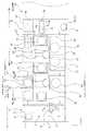
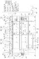
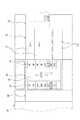
図1は、上記レジスト塗布・現像処理システムの一実施形態の概略平面図、図2は、図1の正面図、図3は、図1の背面図である。 FIG. 1 is a schematic plan view of an embodiment of the resist coating / developing system, FIG. 2 is a front view of FIG. 1, and FIG. 3 is a rear view of FIG.
上記レジスト塗布・現像処理システムは、被処理基板である半導体ウエハW(以下にウエハWという)をウエハカセット1で複数枚例えば25枚単位で外部からシステムに搬入又はシステムから搬出したり、ウエハカセット1に対してウエハWを搬出・搬入したりするためのカセットステーション10(搬出入ブロック)と、塗布現像工程の中で1枚ずつウエハWに所定の処理を施す枚葉式の各種処理ユニットを所定位置に多段配置してなる塗布・現像処理ブロック20(以下に処理ステーション20という)と、この処理ステーション20と隣接して設けられる露光装置40との間でウエハWを受け渡すためのインターフェース部30(インターフェースブロック)と、カセットステーション10と処理ステーション20との間に組み込まれ、レジストパターン表面を平滑化するスムージング処理ユニット51が配置されたスムージング処理ブロック50と、上記処理ステーション20,カセットステーション10,インターフェース部30及びスムージング処理ブロック50の上方から下方に向けて清浄化された空気の流れを形成する気流形成手段60と、気流形成手段60を制御する制御手段100と、で主要部が構成されている。 In the resist coating / development processing system, a plurality of semiconductor wafers W (hereinafter referred to as wafers W), which are substrates to be processed, are carried into or out of the system from the outside in units of a plurality of wafers, for example, 25 wafers. 1 includes a cassette station 10 (unloading / unloading block) for unloading / loading the wafer W to / from the
上記カセットステーション10は、図1に示すように、カセット載置台2上の突起3の位置に複数個例えば4個までの蓋付のウエハカセット1がそれぞれのウエハ出入口を処理ステーション20側に向けて水平のX方向に沿って一列に載置され、各ウエハカセット1に対峙して蓋開閉装置5が配設され、また、カセット配列方向(X方向)及びウエハカセット1内に垂直方向に沿って収容されたウエハWのウエハ配列方向(Z方向)に移動可能なウエハ搬送用ピンセット4が各ウエハカセット1に選択的に搬送するように構成されている。また、ウエハ搬送用ピンセット4は、θ方向に回転可能に構成されており、後述する処理ステーション20側の第3の組G3の多段ユニット部に属するアライメントユニット(ALIM)及びエクステンションユニット(EXT)にも搬送できるようになっている。 As shown in FIG. 1, the
上記処理ステーション20は、図1に示すように、中心部には、移動機構22によって垂直移動する垂直搬送型の主ウエハ搬送アーム21が設けられ、この主ウエハ搬送アーム21の周りに全ての処理ユニットが1組又は複数の組に渡って多段に配置されている。この例では、5組G1,G2,G3,G4及びG5の多段配置構成であり、第1及び第2の組G1,G2の多段ユニットはシステム正面側に並列され、第3の組G3の多段ユニットはカセットステーション10に隣接して配置され、第4の組G4の多段ユニットはインターフェース部30に隣接して配置され、第5の組G5の多段ユニットは背部側に配置されている。 As shown in FIG. 1, the
この場合、図2に示すように、第1の組G1及び第2の組G2では、それぞれカップ(容器)23内でウエハWと現像液供給手段(図示せず)とを対峙させてレジストパターンを現像する現像ユニット(DEV)と、ウエハWをスピンチャック(図示せず)に載置して所定の処理を行うレジスト塗布ユニット(COT)とが垂直方向の下から順に2段に重ねられている。 In this case, as shown in FIG. 2, in the first group G1 and the second group G2, the resist pattern is formed by facing the wafer W and the developer supply means (not shown) in the cup (container) 23, respectively. A developing unit (DEV) that develops the resist and a resist coating unit (COT) that carries out a predetermined process by placing the wafer W on a spin chuck (not shown) are stacked in two stages from the bottom in the vertical direction. Yes.
第3の組G3では、図3に示すように、ウエハWをウエハ載置台24に載置して所定の処理を行うオーブン型の処理ユニット例えばウエハWを冷却するクーリングユニット(COL)、ウエハWに疎水化処理を行うアドヒージョンユニット(AD)、ウエハWの位置合わせを行うアライメントユニット(ALIM)、ウエハWの搬入出を行うエクステンションユニット(EXT)、ウエハWをベークする熱処理装置を使用した4つのホットプレートユニット(HP)が垂直方向の下から順に例えば8段に重ねられている。 In the third group G3, as shown in FIG. 3, an oven-type processing unit for performing a predetermined process by placing the wafer W on the wafer mounting table 24, for example, a cooling unit (COL) for cooling the wafer W, the wafer W In addition, an adhesion unit (AD) for performing a hydrophobic treatment, an alignment unit (ALIM) for aligning the wafer W, an extension unit (EXT) for loading and unloading the wafer W, and a heat treatment apparatus for baking the wafer W were used. Four hot plate units (HP) are stacked in, for example, eight stages in order from the bottom in the vertical direction.
また、第4の組G4では、オーブン型処理ユニット例えばクーリングユニット(COL)、エクステンション・クーリングユニット(EXTCOL)、エクステンションユニット(EXT)、クーリングユニット(COL)、急冷機能を有する熱処理装置を使用した2つのチリングホットプレートユニット(CHP)及び熱処理装置を使用した2つのホットプレートユニット(HP)が垂直方向の下から順に例えば8段に重ねられている。 In the fourth group G4, an oven-type processing unit such as a cooling unit (COL), an extension / cooling unit (EXTCOL), an extension unit (EXT), a cooling unit (COL), or a heat treatment device having a rapid cooling function is used. Two chilling hot plate units (CHP) and two hot plate units (HP) using a heat treatment apparatus are stacked in, for example, eight stages from the bottom in the vertical direction.
上記のように処理温度の低いクーリングユニット(COL)、エクステンション・クーリングユニット(EXTCOL)を下段に配置し、処理温度の高いホットプレートユニット(HP)、チリングホットプレートユニット(CHP)及びアドヒージョンユニット(AD)を上段に配置することで、ユニット間の熱的な相互干渉を少なくすることができる。勿論、ランダムな多段配置とすることも可能である。 As described above, the cooling unit (COL) and the extension cooling unit (EXTCOL) having a low processing temperature are arranged in the lower stage, and the hot plate unit (HP), the chilling hot plate unit (CHP) and the adhesion unit having a high processing temperature. By disposing (AD) in the upper stage, it is possible to reduce thermal mutual interference between units. Of course, a random multi-stage arrangement is also possible.
なお、図1に示すように、処理ステーション20において、第1及び第2の組G1,G2の多段ユニット(スピナ型処理ユニット)に隣接する第3及び第4の組G3,G4の多段ユニット(オーブン型処理ユニット)の側壁の中には、それぞれダクト25,26が垂直方向に縦断して設けられている。これらのダクト25,26には、上記気流形成手段60からのダウンフローの清浄空気が流されるようになっている。このダクト構造によって、第3及び第4の組G3,G4のオーブン型処理ユニットで発生した熱は遮断され、第1及び第2の組G1,G2のスピナ型処理ユニットへは及ばないようになっている。 As shown in FIG. 1, in the
また、この処理システムでは、主ウエハ搬送アーム21の背部側にも図1に点線で示すように第5の組G5の多段ユニットが配置できるようになっている。この第5の組G5の多段ユニットは、案内レール27に沿って主ウエハ搬送アーム21から見て側方へ移動できるようになっている。したがって、第5の組G5の多段ユニットを設けた場合でも、ユニットをスライドすることにより空間部が確保されるので、主ウエハ搬送アーム21に対して背後からメンテナンス作業を容易に行うことができる。なお、処理ステーション20の下部側には、例えばレジスト液,現像液、レジストの溶剤等を貯留するタンク類や、その配管系統を収納するケミカルユニット29が設けられている。 Further, in this processing system, a fifth stage G5 multi-stage unit can be arranged on the back side of the main
上記インターフェース部30は、奥行き方向では処理ステーション20と同じ寸法を有するが、幅方向では小さなサイズに作られている。このインターフェース部30の正面部には可搬性のピックアップカセット31と定置型のバッファカセット32が2段に配置され、背面部には、ウエハWの周辺部の露光及び識別マーク領域の露光を行う露光手段である周辺露光装置33が配設され、中央部には、搬送手段であるウエハの搬送アーム34が配設されている。この搬送アーム34は、X,Z方向に移動して両カセット31,32及び周辺露光装置33に搬送するように構成されている。また、搬送アーム34は、θ方向に回転可能に構成され、処理ステーション20側の第4の組G4の多段ユニットに属するエクステンションユニット(EXT)及び隣接する露光装置側のウエハ受渡し台(図示せず)にも搬送できるように構成されている。 The
上記スムージング処理ブロック50には、レジストパターンが形成され、露光後の現像処理がされたウエハWのレジストパターンの表面にレジストの溶剤蒸気を供給してレジストパターン表面を平滑化するスムージング処理ユニット51と、スムージング処理前のウエハWの表面に形成されたレジストパターンの溶解阻害性保護基を分離するための紫外線をウエハWの表面に照射する紫外線照射ユニット52と、スムージング処理後のウエハWに付着する溶剤雰囲気を蒸発するための熱処理ユニット53と、スムージング処理ユニット51と紫外線照射ユニット52又は熱処理ユニット53との間でウエハWを受け渡しするウエハ搬送アーム54(基板搬送アーム)が配置(配設)されている。このウエハ搬送アーム54は、移動機構54aによって垂直のZ方向及び水平のX,Y方向に移動可能に形成されている。なお、スムージング処理ブロック50のカセットステーション10側には、アライメントユニット(ALIM)が配置されている。 In the smoothing
この場合、スムージング処理ユニット51は、図4及び図5に示すように、筐体56内の中央部には、ウエハWを保持するチャック57が設けられている。チャック57の上面の保持面57aは、水平でウエハWの径と同程度の円形状に形成されている。チャック57の保持面57aには、図示しない複数の吸引口が設けられており、この吸引口から吸引することによりウエハWを吸着できる。なお、チャック57には、シリンダなどの昇降駆動部58が設けられており、チャック57の保持面57aを上下動させて、主ウエハ搬送アーム21との間でウエハWを受け渡しできるようになっている。 In this case, as shown in FIGS. 4 and 5, the smoothing
なお、筐体56の一側部56aにはウエハWの搬入出口56bが設けられており、この搬入出口56bには図示しない開閉機構によって搬入出口56bを開閉するシャッタ56cが配設されている。また、筐体56の下部側方には排気口56dが形成されている。この排気口56dは、排気管56eを介して排気手段例えば排気ポンプ(図示せず)に接続されている。 A loading / unloading
チャック57の周囲には、例えば排気用のカップ59が設けられている。カップ59は、例えばチャック57の保持面57aの下方に位置している。カップ59は、例えば円筒状の外カップ59aと内カップ59bからなる二重構造に形成され、外カップ59aと内カップ59bとの間に排気通路59cが形成されている。外カップ59aと内カップ59bとの上端部の隙間には、環状の吸入口59dが開口し、この吸入口59dは、図4に示すように、保持面57aの周縁部に沿うように配置されている。外カップ59aと内カップ59bとの下端部の隙間には、排気装置(図示せず)に通じる排気管59eが接続されており、チャック57上の雰囲気を吸入口59dから適宜排気できるようになっている。 For example, an
また、図5に示すように、カップ59のX方向負方向(図5の上方向)側の側方には、Y方向(図5の左右方向)に沿ったレール72が設けられている。レール72は、例えばカップ59の一端部側の外方から他端部側の外方まで設けられている。レール72上には、アーム73が設けられ、アーム73は、駆動部74によってレール72上を移動自在に形成されている。アーム73には、ウエハWに溶剤蒸気を吐出するノズルとしての溶剤蒸気供給ノズル71(以下に溶剤供給ノズル71という)が保持されている。したがって、溶剤供給ノズル71は、レール72に沿ってカップ59の一端部側の外方からチャック57上を通過しカップ59の他端部側の外方まで移動できる。また、溶剤供給ノズル71の移動は、例えば駆動部74の動作を制御する駆動制御部75により制御されており、この駆動制御部75により、溶剤供給ノズル71をY方向に所定の速度で移動させることができる。また、駆動部74は、例えばアーム73を上下動させるシリンダなどを備え、溶剤供給ノズル71の高さを調整することができる。なお、本実施の形態においては、レール72,アーム73,駆動部74及び駆動制御部75によって移動機構が構成されている。 As shown in FIG. 5, rails 72 along the Y direction (left and right direction in FIG. 5) are provided on the side of the
溶剤供給ノズル71は、例えばウエハWの直径よりも長いX方向に沿った細長形状を有し、溶剤供給ノズル71の下面には、長手方向の一端部から他端部に渡って吐出部71aが形成されている。吐出部71aには、溶剤供給ノズル71の長手方向に沿って円形の吐出口(図示せず)が複数形成されている。例えば、溶剤供給ノズル71の上部には、図4に示すように、溶剤蒸気供給源70に通じる溶剤蒸気供給管路76が接続されている。溶剤供給ノズル71は、上部から溶剤蒸気を導入し、この溶剤蒸気を内部に流通させ、溶剤蒸気を下面の各吐出口から下方に向けて均等に吐出できるようになっている。 The
溶剤蒸気供給源70は、例えば溶剤蒸気供給管路76と接続し液体溶剤が貯留された溶剤蒸気生成用の貯留タンク77aと、不活性の窒素(N2)ガスの供給源78に接続し貯留タンク77a内に溶剤蒸気を圧送するためのN2ガスを供給するN2ガス供給管路76Aを備えている。このN2ガス供給管路76Aには、気体流量調整弁78aが介設されている。このように構成されるN2ガス供給管路76Aから貯留タンク77aの液体溶剤内にN2ガスを供給することによって、貯留タンク77a内で気化している溶剤蒸気が溶剤蒸気供給管路76内に圧送され、溶剤蒸気が溶剤蒸気供給管路76を通って溶剤供給ノズル71に供給される。溶剤としては、例えばアセトン,プロピレングリコールモノメチルエーテルアセテート(PGMEA),Nメチル2ピロリジノン(NMP)を用いることができる。 The solvent
また、溶剤蒸気供給管路76には,溶剤蒸気の流量を検出する流量センサ79aと、流量を調節する流量調整バルブ79bが設けられている。流量センサ79aで検出された検出結果は、流量制御部79cに出力され、流量制御部79cは、検出結果に基づいて流量調整バルブ79bの開閉度を調整して溶剤供給ノズル71から吐出される溶剤蒸気の流量を所定の流量に設定できる。この場合、流量制御部79cは制御手段であるコントローラ100に電気的に接続されており、コントローラ100からの制御信号に基づいて溶剤蒸気の流量が調節される。なお、溶剤蒸気供給管路76には、温調部76aが設けられており、この温調部76aによって、溶剤供給ノズル71に供給される溶剤蒸気の温度が一定の温度に維持されるようになっている。 The solvent
また、貯留タンク77aの外側部及び底部には温度調整用のヒータ80が配置されており、ヒータ80は加熱電源81によって所定温度に加熱される。また、貯留タンク77a内には、この貯留タンク77a内の温度を検出する温度センサ82と、貯留タンク77a内の溶剤液面の高さを検出する液面高さセンサ83が配設されている。 Further, a
なお、温度センサ82,液面高さセンサ83,加熱電源81,気体流量調整弁78a及び温調部76aは、コントローラ100に電気的に接続されており、温度センサ82と液面高さセンサ83によって検出された検出信号は、コントローラ100に伝達され、コントローラ100からの制御信号が加熱電源81,気体流量調整弁78a,流量制御部79c及び温調部76aに伝達されて、加熱電源81,気体流量調整弁78a,流量制御部79c及び温調部76aが制御されるようになっている。 The temperature sensor 82, the
上記のように構成されるスムージング処理ユニット51において、ウエハWがチャック57の保持面57aに保持されると、溶剤供給ノズル71がカップ59の外方からウエハWの一端部から上方まで移動する。そして、例えばカップ59からの排気が一旦停止され、溶剤供給ノズル71から一定流量の溶剤蒸気が吐出され始める。このときウエハ表面の一端部側の所定量域に溶剤蒸気が供給され、溶剤供給ノズル71から溶剤蒸気が吐出され始めると、溶剤供給ノズル71が一定速度でウエハWの他端部側、つまりY方向負方向側に向かって移動し、これに伴ってウエハ表面上における溶剤蒸気の供給領域もY方向負方向側に移動する。そして、溶剤供給ノズル71がウエハWのY方向負方向側の端部の上方まで移動すると、今度は、折り返しウエハWの他端部側から一端部側に移動する。このようにして、溶剤供給ノズル71がウエハW上を往復移動し、ウエハW上のレジスト膜の表面に溶剤蒸気が供給される。 In the smoothing
このようにして、レジスト膜の表面に溶剤蒸気が供給されると、レジストパターンの表面が溶剤蒸気を取り込んで、レジストパターンの表面のみが溶解し膨潤する。なお,このときの溶剤供給ノズル71の移動速度,吐出量,溶剤濃度及び温度等の設定には、レジストパターンの表面のみが溶解するように予め実験等で算出された値が用いられる。 In this way, when the solvent vapor is supplied to the surface of the resist film, the surface of the resist pattern takes in the solvent vapor, and only the surface of the resist pattern dissolves and swells. At this time, for the setting of the moving speed, the discharge amount, the solvent concentration, the temperature, and the like of the
上記紫外線照射ユニット52は、図6に示すように、処理容器52a内に回転載置台52bを具備し、処理容器52a内の上面には紫外線の照射部52cを具備している。また、処理容器52aの側部にはウエハ搬入出口52dが設けられ、このウエハ搬入出口52dは、図示しない開閉機構によって開閉自在なシャッタ52eが設けられている。 As shown in FIG. 6, the
このように構成される紫外線照射ユニット52において、回転載置台52b上に載置されたウエハWを回転させながら、照射部52cから紫外線をウエハWに照射することにより、ウエハW表面の処理膜、例えばレジスト膜を改質して、溶解阻害性保護基を分解することができる。また、ウエハWを回転させながら照射しているので、ウエハWに対して均一に紫外線や電子線を照射することが可能である。 In the
このようにして、ウエハWの処理膜中の溶解阻害性保護基を分解してから、上述したような溶剤蒸気を供給することで、たとえレジスト膜がArFレジストであっても、これを好適にスムージングすることが可能である。しかも、このようないわば前処理をすることにより、今まで効き目が無かった溶剤を使用してもスムージングすることができるので、溶剤選択の幅が広がる。そして、溶剤選択の幅が増えることにより、各ArFレジスト合った溶剤が選択でき、形状等のコントロール性能も優位になる。 In this way, by dissolving the dissolution inhibiting protective group in the processing film of the wafer W and then supplying the solvent vapor as described above, even if the resist film is an ArF resist, Smoothing is possible. In addition, by performing such pretreatment, smoothing can be performed even with a solvent that has not been effective until now, so that the range of solvent selection is widened. Further, by increasing the range of solvent selection, a solvent suitable for each ArF resist can be selected, and the control performance of the shape and the like becomes superior.
上記熱処理ユニット53は、図7に示すように、筐体53a内にウエハWを載置し加熱する熱板53bを具備している。熱板53b内には、給電により発熱するヒータ53cが内蔵されている。ヒータ53cの電源53dは、ヒータ制御部53eにより制御されており、ヒータ制御部53eは、上記コントローラ100と電気的に接続されており、コントローラ100からの制御信号に基づいてヒータ53cの発熱量を調節して熱板53bの温度を制御できる。また、筐体53aの側部にはウエハ搬入出口53fが設けられ、このウエハ搬入出口53fは、図示しない開閉機構によって開閉自在なシャッタ53gが設けられている。 As shown in FIG. 7, the
なお、熱板53bの中央部には、上下方向に貫通した貫通孔53hが形成されている。貫通孔53hには、下方から昇降ピン53iが挿入されている。昇降ピン53iは、昇降機構53jにより昇降し、熱板53bの表面に突出自在になっている。したがって、ウエハWを昇降ピン53iにより持ち上げて例えば主ウエハ搬送アーム54と熱板53bとの間でウエハWの受け渡しを行うことができる。 A through-
一方、上記気流形成手段60は、図2に示すように、カセットステーション10,スムージング処理ブロック50,処理ステーション20及びインターフェース部30の上端部に水平に配置され、図示しない空気供給機構に接続する主通気ダクト61を具備している。主通気ダクト61は、処理ステーション20の上部に設けられた第1の空気供給室62aに連通する第1の通気路63aと、スムージング処理ブロック50の上部に設けられた空気供給室62bに連通する第2の通気路63bと、カセットステーション10の上部に設けられた空気供給室62cに連通する第3の通気路63c及びインターフェース部30の上部に設けられた空気供給室62dに連通する第4の通気路63dに連通されている。第1ないし第4の通気路63a,63b,63c,63d内には、それぞれ第1ないし第4の流量調整弁64a,64b,64c,64dが介設されている。また、各空気供給室62a,62b,62c,62d内には例えばHEPAフィルタを有するフィルタユニットFUが配置されており、主通気ダクト61から第1ないし第4の流量調整弁64a,64b,64c,64dを介して供給される空気を清浄化して、処理ステーション20,スムージング処理ブロック50,カセットステーション10及びインターフェース部30へダウンフローにより供給している。この場合、第1ないし第4の流量調整弁64a,64b,64c,64dは、コントローラ100と電気的に接続されており、コントローラ100からの制御信号に基づいて第1ないし第4の流量調整弁64a,64b,64c,64dの開度が調節されるようになっている。 On the other hand, as shown in FIG. 2, the airflow forming means 60 is disposed horizontally at the upper end of the
上記処理ステーション20,スムージング処理ブロック50,カセットステーション10及びインターフェース部30内には、それぞれの内部圧力を検出する第1ないし第4の圧力センサ65a,65b,65c,65dが配置されている。これら圧力センサ65a,65b,65c,65dは、コントローラ100に電気的に接続されており、圧力センサ65a,65b,65c,65dによって検出された検知信号はコントローラ100に伝達され、コントローラ100からの制御信号に基づいて、第1ないし第4の流量調整弁64a,64b,64c,64dの開度が調整されて、処理ステーション20,スムージング処理ブロック50,カセットステーション10及びインターフェース部30への空気の供給量が調整される。 In the
この調整により、スムージング処理ブロック50内の圧力が処理ステーション20内の圧力より低く設定される。これにより、スムージング処理ブロック50に対して処理ステーション20内が陽圧となり、スムージング処理ブロック50内に発生した溶剤雰囲気が処理ステーション20内に侵入するのを防止することができ、処理ステーション20内の処理ユニット例えばレジスト塗布ユニット(COT)や現像ユニット(DEV)等が溶剤雰囲気によって汚染されるのを防止することができる。また、処理ステーション20を介して露光装置40内に溶剤雰囲気が侵入するのを防止することができ、露光装置40内が溶剤雰囲気によって汚染されるのを防止することができる。 By this adjustment, the pressure in the smoothing
また、第2,第3の流量調整弁64b,64cの調整により、スムージング処理ブロック50内の圧力がカセットステーション10内の圧力より低く設定される。これにより、スムージング処理ブロック50に対してカセットステーション10内が陽圧となり、スムージング処理ブロック50内に発生した溶剤雰囲気がカセットステーション10内に侵入するのを防止することができ、カセットステーション10内の処理ユニットやウエハWが溶剤雰囲気によって汚染されるのを防止することができる。 Further, the pressure in the smoothing
また、スムージング処理ブロック50内には、スムージング処理ブロック50内の処理ユニット外の溶剤雰囲気を検出するガス濃度センサ66が配設されている。このガス濃度センサ66は、コントローラ100に電気的に接続されており、ガス濃度センサ66によって検出された検知信号はコントローラ100に伝達され、コントローラ100からの制御信号に基づいて、上記溶剤蒸気供給源70の加熱電源81,気体流量調整弁78a,流量制御部79c及び温調部76aが制御されて、スムージング処理ブロック50内のスムージング処理ユニット51に供給される溶剤蒸気の濃度が所定濃度に調整される。 Further, a
また、スムージング処理ブロック50の下部に設けられた排気ダクト67には、スムージング処理ブロック50内の溶剤雰囲気を捕集するケミカルフィルタ68が配置されている。このケミカルフィルタ68の下流側には、ガス漏れ検知センサ69が配設されている。このガス漏れ検知センサ69はコントローラ100と電気的に接続されており、ガス漏れ検知センサ69の検出信号がコントローラ100に伝達され、コントローラ100により例えばアラームやモニタ等の表示手段90に検出情報が表示されるようになっている。例えば、ガス漏れ検知センサ69によって溶剤雰囲気の漏れを検知した場合は、コントローラ100からの制御信号に基づいて表示手段90からアラームが発せられるようになっている。 In addition, a
次に、上記のように構成されたスムージング処理ブロック50を備えたレジスト塗布・現像処理システムの動作態様について説明する。 Next, an operation mode of the resist coating / development processing system including the smoothing
まず、カセットステーション10において、蓋開閉装置5が作動して先行のロットのウエハカセット1の蓋を開放する。次に、ウエハ搬送用ピンセット4がカセット載置台2上の未処理のウエハWを収容しているカセット1にアクセスして、そのカセット1から1枚の未処理のウエハWを取り出す。ウエハ搬送用ピンセット4は、カセット1よりウエハWを取り出すと、スムージング処理ブロック50側のアライメントユニット(ALIM)まで移動し、アライメントユニット(ALIM)内のウエハ載置台55上にウエハWを載せる。ウエハWは、ウエハ載置台55上でオリフラ合せ及びセンタリングを受ける。すると、ウエハ搬送アーム54がアライメントユニット(ALIM)に反対側からアクセスし、ウエハ載置台55からウエハWを受け取って、処理ステーション20側の第3の組G3の多段ユニット内に配置されているアライメントユニット(ALIM)まで移動し、アライメントユニット(ALIM)内のウエハ載置台24上にウエハWを載せる。ウエハWは、ウエハ載置台24上でオリフラ合せ及びセンタリングを受ける。その後、主ウエハ搬送アーム21がアライメントユニット(ALIM)に反対側からアクセスし、ウエハ載置台24からウエハWを受け取る。 First, in the
処理ステーション20において、主ウエハ搬送アーム21はウエハWを最初に第3の組G3の多段ユニットに属するアドヒージョンユニット(AD)に搬入する。このアドヒージョンユニット(AD)内でウエハWは疎水化処理を受ける。疎水化処理が終了すると、主ウエハ搬送アーム21は、ウエハWをアドヒージョンユニット(AD)から搬出して、次に第3の組G3又は第4の組G4の多段ユニットに属するクーリングユニット(COL)へ搬入する。このクーリングユニット(COL)内でウエハWはレジスト塗布処理前の設定温度例えば23℃まで冷却される。冷却処理が終了すると、主ウエハ搬送アーム21は、ウエハWをクーリングユニット(COL)から搬出し、次に第1の組G1又は第2の組G2の多段ユニットに属するレジスト塗布ユニット(COT)へ搬入する。このレジスト塗布ユニット(COT)内でウエハWはスピンコート法によりウエハ表面に一様な膜厚でレジストを塗布する。 In the
レジスト塗布処理が終了すると、主ウエハ搬送アーム21は、ウエハWをレジスト塗布ユニット(COT)から搬出し、次にホットプレートユニット(HP)内へ搬入する。ホットプレートユニット(HP)内でウエハWは載置台上に載置され、所定温度例えば100℃で所定時間プリベーク処理される。これによって、ウエハW上の塗布膜から残存溶剤を蒸発除去することができる。プリベークが終了すると、主ウエハ搬送アーム21は、ウエハWをホットプレートユニット(HP)から搬出し、次に第4の組G4の多段ユニットに属するエクステンション・クーリングユニット(EXTCOL)へ搬送する。このユニット(EXTCOL)内でウエハWは次工程すなわち周辺露光装置33における周辺露光処理に適した温度例えば24℃まで冷却される。この冷却後、主ウエハ搬送アーム21は、ウエハWを直ぐ上のエクステンションユニット(EXT)へ搬送し、このユニット(EXT)内の載置台(図示せず)の上にウエハWを載置する。このエクステンションユニット(EXT)の載置台上にウエハWが載置されると、インターフェース部30の搬送アーム34が反対側からアクセスして、ウエハWを受け取る。そして、搬送アーム34はウエハWをインターフェース部30内の周辺露光装置33へ搬入する。周辺露光装置33において、ウエハW表面の周辺部の余剰レジスト膜(部)に光が照射されて周辺露光が施される。 When the resist coating process is completed, the main
周辺露光が終了した後、搬送アーム34が周辺露光装置33の筐体内からウエハWを搬出し、隣接する露光装置40側のウエハ受取り台(図示せず)へ移送する。 After the peripheral exposure is completed, the
露光装置40で全面露光が済んで、ウエハWが露光装置40側のウエハ受取り台に戻されると、インターフェース部30の搬送アーム34はそのウエハ受取り台へアクセスしてウエハWを受け取り、受け取ったウエハWを処理ステーション20側の第4の組G4の多段ユニットに属するエクステンションユニット(EXT)へ搬入し、ウエハ受取り台上に載置する。 When the entire exposure is completed in the
ウエハ受取り台上に載置されたウエハWは、主ウエハ搬送アーム21により、チリングホットプレートユニット(CHP)に搬送(搬入)され、フリンジの発生を防止するため、あるいは化学増幅型レジスト(CAR)における酸触媒反応を誘起するため、例えば120℃で所定時間ポストエクスポージャーベーク処理が施される。 The wafer W placed on the wafer receiving table is transferred (carried in) to the chilling hot plate unit (CHP) by the main
その後、ウエハWは、第1の組G1又は第2の組G2の多段ユニットに属する現像ユニット(DEV)に搬入される。この現像ユニット(DEV)内では、ウエハW表面のレジストに現像液が満遍なく供給されて現像処理が施される。この現像処理によって、ウエハW表面に形成されたレジスト膜が所定の回路パターンに現像されると共に、ウエハWの周辺部の余剰レジスト膜が除去され、更に、ウエハW表面に形成された(施された)アライメントマークの領域に付着したレジスト膜が除去される。このようにして、現像が終了すると、ウエハW表面にリンス液がかけられて現像液が洗い落とされる。 Thereafter, the wafer W is carried into a developing unit (DEV) belonging to the multistage unit of the first group G1 or the second group G2. In the developing unit (DEV), a developing solution is uniformly supplied to the resist on the surface of the wafer W to perform a developing process. By this development processing, the resist film formed on the surface of the wafer W is developed into a predetermined circuit pattern, and the surplus resist film in the peripheral portion of the wafer W is removed, and further, the resist film formed on the surface of the wafer W is applied (applied). E) The resist film adhering to the alignment mark region is removed. In this way, when the development is completed, a rinse liquid is applied to the surface of the wafer W to wash away the developer.
現像工程が終了すると、主ウエハ搬送アーム21は、ウエハWを現像ユニット(DEV)から搬出して、アライメントユニット(ALIM)内のウエハ載置台24上にウエハWを載せる。ウエハWは、ウエハ載置台24上でオリフラ合せ及びセンタリングを受ける。その後、ウエハ搬送アーム54がアライメントユニット(ALIM)に反対側からアクセスし、ウエハ載置台24からウエハWを受け取って、スムージング処理ブロック50内の紫外線照射ユニット52内に搬入する。そして、紫外線照射ユニット52の回転載置台52b上に載置されたウエハWを回転させながら、照射部52cから紫外線をウエハWに照射することにより、ウエハW表面のレジスト膜、例えばレジストパターンを改質して、溶解阻害性保護基を分解する。 When the developing process is completed, the main
紫外線照射ユニット52によって紫外線が照射されたウエハWはウエハ搬送アーム54によって紫外線照射ユニット52から搬出され、次にスムージング処理ユニット51に搬入される。そして、上述したように、スムージング処理ユニット51に搬入されたウエハWは、チャック57の保持面57aに保持される。この状態で、溶剤供給ノズル71がウエハW上を往復移動し、ウエハW上のレジストパターンの表面に溶剤蒸気を供給してレジストパターンを膨潤させ、レジストパターンの表面の凹凸を均し平滑化(スムージング)する。 The wafer W irradiated with ultraviolet rays by the
スムージング処理ユニット51によってスムージング処理されたウエハWは、ウエハ搬送アーム54によってスムージング処理ユニット51から搬出され、次に熱処理ユニット53に搬入される。熱処理ユニット53に搬入されたウエハWは、熱板53b上に載置され、熱板53bに内蔵されたヒータ53cによって例えば100℃で所定時間、加熱処理される。これによって、ウエハWに付着する溶剤が蒸発されると共に、現像で膨潤したレジストが硬化し、耐薬品性が向上する。 The wafer W smoothed by the smoothing
熱処理ユニット53によって溶剤が蒸発されたウエハWはウエハ搬送アーム54によって熱処理ユニット53から搬出され、カセットステーション10側のアライメントユニット(ALIM)内のウエハ載置台55上にウエハWを載せる。ウエハWは、ウエハ載置台55上でオリフラ合せ及びセンタリングを受ける。その後、ウエハ搬送用ピンセット4がアライメントユニット(ALIM)に反対側からアクセスし、ウエハ載置台55からウエハWを受け取る。そして、ウエハ搬送用ピンセット4は、受け取った処理済みのウエハWをカセット載置台上の処理済みウエハ収容用のウエハカセット1の所定のウエハ収容溝に入れ、ウエハカセット1内に全ての処理済みのウエハWが収納された後、蓋開閉装置5が作動して蓋を閉じて処理が完了する。 The wafer W from which the solvent has been evaporated by the
なお、上記実施形態では、スムージング処理ブロック50内に配置されるスムージング処理ユニット51が上下に段状に配置される場合について説明したが、スムージング処理ユニット51の配置形態は任意であり、例えば、スムージング処理ユニット51を左右に並設して配置してもよい。また、紫外線照射ユニット52や熱処理ユニット53の配置形態も任意であり、必要に応じて上下に段状に配置するか、左右に並設して配置してもよい。 In the above embodiment, the case has been described where the smoothing
また、上記実施形態では、スムージング処理ブロック50をカセットステーション10と処理ステーション20の間に配設した場合について説明したが、必ずしもこのような配置形態とする必要はない。例えば、スムージング処理ブロック50を、連設するカセットステーション10と処理ステーション20に対して平面視において直交するようにしてカセットステーション10に連設することも可能である。 Moreover, although the case where the smoothing
W 半導体ウエハ(被処理基板)
10 カセットステーション(搬出入ブロック)
20 処理ステーション(塗布・現像処理ブロック)
30 インターフェース部(インターフェースブロック)
40 露光装置
50 スムージング処理ブロック
51 スムージング処理ユニット
52 紫外線照射ユニット
53 熱処理ユニット
54 ウエハ搬送アーム(基板搬送アーム)
60 気流形成手段
63a〜63d 第1〜第4の通気路
64a〜64d 第1〜第4の流量調整弁
65a〜65d 第1〜第4の圧力センサ
66 ガス濃度センサ
67 排気ダクト
68 ケミカルフィルタ
69 ガス漏れ検知センサ
70 溶剤蒸気供給源
71 溶剤供給ノズル(溶剤蒸気供給ノズル)
76a 温調部
77a 貯留タンク
78a 気体流量調整弁
79a 流量センサ
79b 流量調整バルブ
79c 流量制御部
80 温度調整用ヒータ
82 温度センサ
83 液面高さセンサ
90 表示手段
100 コントローラ(制御手段)W Semiconductor wafer (substrate to be processed)
10 Cassette station (carrying in / out block)
20 processing station (coating / development processing block)
30 Interface section (interface block)
40
60 Airflow forming means 63a-63d 1st-
76a
Claims (5)
Translated fromJapanese複数枚の基板を収納するカセットから上記塗布・現像処理ブロック側へ未処理の基板を搬入すると共に、処理済みの基板をカセットに収納する搬出入ブロックと、
上記塗布・現像処理部ブロック内の現像処理ユニットによりレジストパターンが形成されるように露光後の基板に現像処理がされ、その基板のレジストパターンの表面にレジストの溶剤蒸気を供給してレジストパターン表面を平滑化するスムージング処理ユニットが配置されると共に、上記搬出入ブロックと上記塗布・現像処理部ブロックとの間に隣接して配置されたスムージング処理ブロックと、
上記塗布・現像処理ブロック、搬出入ブロック、スムージング処理ブロックの上方から下方に向けて空気の流れを形成する気流形成手段と、
上記スムージング処理ブロック内に設けられ、スムージング処理ユニット外の上記溶剤雰囲気のガス濃度を検出するガス濃度センサと、
上記スムージング処理ユニットに接続された溶剤蒸気を供給する溶剤蒸気供給源に備えられる、溶剤蒸気の温度調整用の加熱電源と、溶剤蒸気を圧送するための気体流量を調整する気体流量調整弁と、上記溶剤蒸気の流量制御部と、上記気流形成手段とを制御する制御手段と、を具備し、
上記制御手段は、上記塗布・現像処理ブロック内の圧力を検出する第1の圧力センサ、上記スムージング処理ブロック内の圧力を検出する第2の圧力センサ及び上記搬出入ブロック内の圧力を検出する第3の圧力センサからの検出信号に基づいて、上記気流形成手段における上記塗布・現像処理ブロックへの通気路に介設される第1の流量調整弁と、上記スムージング処理ブロックへの通気路に介設される第2の流量調整弁と、上記気流形成手段における上記搬出入ブロックへの通気路に介設される第3の流量調整弁とを制御することにより、上記スムージング処理ブロック内の圧力が上記塗布・現像処理ブロック内の圧力及び上記搬出入ブロック内の圧力より低くなるようにすると共に、上記ガス濃度センサの検出した検知信号に基づいて、上記加熱電源と気体流量調整弁及び流量制御部を制御することにより、上記スムージング処理ユニットに供給する溶剤蒸気の濃度を所定濃度に調整する、ことを特徴とする基板処理装置。A coating / development processing block in which a plurality of processing units for performing resist coating and development processing on the substrate are disposed;
A loading / unloading block for loading an unprocessed substrate from the cassette storing a plurality of substrates to the coating / development processing block side, and storing the processed substrate in the cassette;
Developingthe substrate after exposure to a resist pattern is formedby development processing unit of the coating and developing processing unit blockis, the resist pattern surface by supplying a solvent vapor of the resist on the surface of the resist pattern ofthe substrate a smoothing blockdisposed adjacent between the is disposed smoothing unit for smoothingRutotomoni, the loading and unloading block and the coating and developing processing unit blocks,
An air flow forming means for forming an air flow from the upper side to the lower side of the coating / development processing block, the carry-in / out block, and the smoothing processing block;
A gas concentration sensor provided in the smoothing processing block for detecting the gas concentration of the solvent atmosphere outside the smoothing processing unit;
A heating source for adjusting the temperature of the solvent vapor, provided in a solvent vapor supply source for supplying the solvent vapor connected to the smoothing processing unit, a gas flow rate adjusting valve for adjusting the gas flow rate for pumping the solvent vapor, A control meansfor controllingthe flow rate control unit of the solvent vapor and the airflow forming means,
The control means,first detects the pressure of the first pressuresensor, the smoothing processing second pressure sensorand the loading and unloading block for detecting the pressure in the block for detecting the pressure of the coating and developing processing block3 on the basis of the detection signal fromthe pressure sensor 3, the first flow rate adjusting valve provided in the air flow path to the coating / development processing block in the air flow forming means, and the air flow path to the smoothing processing block. By controlling the second flow rate adjusting valve provided and the third flow rate adjusting valve provided inthe air passage to the carry-in / out block in the air flow forming means , the pressure in thesmoothing processing block is increased.together to be lower than thepressure of the pressureand the loading and unloading a block of the coating and developing processingblock, based on the detected detection signal of the gas concentration sensor Said by controlling the heating power and the gas flow control valve and flow rate control unit is adjusted to a predetermined concentration the concentration of the solvent vapor supplied to the smoothing processing unit, the substrate processing apparatus, characterized in that.
上記スムージング処理ブロックの下部排気側に、溶剤雰囲気を捕集するフィルタを配置すると共に、該フィルタの下流側にガス漏れ検知センサを配設し、該ガス漏れ検知センサの検出信号に基づいて上記制御手段により表示手段に検出情報を表示可能に形成してなる、ことを特徴とする基板処理装置。The substrate processing apparatus according to claim1 ,
A filter for collecting the solvent atmosphere is disposed on the lower exhaust side of the smoothing processing block, and a gas leak detection sensor is disposed on the downstream side of the filter, and the control is performed based on a detection signal of the gas leak detection sensor. The substrate processing apparatus is characterized in that the detection information can be displayed on the display means by the means.
上記スムージング処理ブロック内に、スムージング処理後の基板に付着する溶剤雰囲気を蒸発するための熱処理ユニットを配置すると共に、該熱処理ユニットと上記スムージング処理ユニットとの間で基板を受け渡しする基板搬送アームを配設してなる、ことを特徴とする基板処理装置。In the substrate processing apparatus according to claim 1or 2 ,
A heat treatment unit for evaporating the solvent atmosphere adhering to the substrate after the smoothing process is disposed in the smoothing processing block, and a substrate transfer arm for transferring the substrate between the heat treatment unit and the smoothing process unit is disposed. A substrate processing apparatus, characterized by comprising:
上記スムージング処理ブロック内に、レジストパターンの溶解阻害性保護基を分離するための紫外線を基板の表面に照射する紫外線照射ユニットを配置すると共に、該紫外線照射ユニットと上記スムージング処理ユニットとの間で基板を受け渡しする基板搬送アームを配設してなる、ことを特徴とする基板処理装置。The substrate processing apparatus according to any one of claims 1 to3 ,
In the smoothing processing block, an ultraviolet irradiation unit for irradiating the surface of the substrate with ultraviolet light for separating the dissolution inhibiting protective group of the resist pattern is disposed, and the substrate is disposed between the ultraviolet irradiation unit and the smoothing processing unit. A substrate processing apparatus comprising a substrate transfer arm for delivering and receiving.
上記スムージング処理ユニットにおける溶剤蒸気供給手段は、基板の表面に溶剤蒸気を吐出するノズルと、溶剤を収容する溶剤蒸気生成用のタンクと、該タンクと内に溶剤蒸気圧送用の気体を供給する気体供給源と、上記ノズルとタンクを接続する溶剤蒸気供給管路と、を具備し、
上記タンクには、該タンク内の温度を検出する温度センサと、タンク内の溶剤液面の高さを検出する液面高さセンサと、を具備し、
上記タンクと気体供給源とを接続する気体供給管路に気体流量調整弁を介設すると共に、上記溶剤蒸気供給管路に溶剤蒸気の流量調整弁を介設し、
上記ガス濃度センサ、温度センサ及び液面高さセンサからの検出信号に基づいて上記制御手段により、上記気体流量調整弁及び溶剤蒸気の流量調整弁を制御すると共に、上記表示手段に検出情報を表示可能にする、ことを特徴とする基板処理装置。The apparatus according to any one of claims 1 to4,
The solvent vapor supply means in the smoothing processing unit includes a nozzle that discharges the solvent vapor onto the surface of the substrate, a solvent vapor generation tank that contains the solvent, and a gas that supplies a gas for solvent vapor pressure feeding into the tank. A supply source, and a solvent vapor supply line connecting the nozzle and the tank,
The tank includes a temperature sensor for detecting the temperature in the tank, and a liquid level sensor for detecting the height of the solvent level in the tank,
A gas flow rate adjustment valve is provided in the gas supply line connecting the tank and the gas supply source, and a solvent vapor flow rate adjustment valve is provided in the solvent vapor supply line,
The control means controls the gas flow rate adjustment valve and the solvent vapor flow rate adjustment valve based on detection signals from the gas concentration sensor, temperature sensor, and liquid level sensor, and also displays detection information on the display means. A substrate processing apparatus characterized by being enabled.
Priority Applications (4)
| Application Number | Priority Date | Filing Date | Title |
|---|---|---|---|
| JP2007325718AJP4601080B2 (en) | 2007-12-18 | 2007-12-18 | Substrate processing equipment |
| TW097145460ATWI379371B (en) | 2007-12-18 | 2008-11-25 | Substrate processing device |
| US12/336,711US8033244B2 (en) | 2007-12-18 | 2008-12-17 | Substrate processing system |
| KR1020080129320AKR101359804B1 (en) | 2007-12-18 | 2008-12-18 | Substrate processing system |
Applications Claiming Priority (1)
| Application Number | Priority Date | Filing Date | Title |
|---|---|---|---|
| JP2007325718AJP4601080B2 (en) | 2007-12-18 | 2007-12-18 | Substrate processing equipment |
Publications (2)
| Publication Number | Publication Date |
|---|---|
| JP2009147261A JP2009147261A (en) | 2009-07-02 |
| JP4601080B2true JP4601080B2 (en) | 2010-12-22 |
Family
ID=40751565
Family Applications (1)
| Application Number | Title | Priority Date | Filing Date |
|---|---|---|---|
| JP2007325718AExpired - Fee RelatedJP4601080B2 (en) | 2007-12-18 | 2007-12-18 | Substrate processing equipment |
Country Status (4)
| Country | Link |
|---|---|
| US (1) | US8033244B2 (en) |
| JP (1) | JP4601080B2 (en) |
| KR (1) | KR101359804B1 (en) |
| TW (1) | TWI379371B (en) |
Families Citing this family (20)
| Publication number | Priority date | Publication date | Assignee | Title |
|---|---|---|---|---|
| US7875420B2 (en)* | 2003-06-06 | 2011-01-25 | Tokyo Electron Limited | Method for improving surface roughness of processed film of substrate and apparatus for processing substrate |
| JP5437739B2 (en)* | 2009-08-21 | 2014-03-12 | 東京エレクトロン株式会社 | Liquid processing system |
| JP5639816B2 (en)* | 2009-09-08 | 2014-12-10 | 東京応化工業株式会社 | Coating method and coating apparatus |
| JP5439097B2 (en)* | 2009-09-08 | 2014-03-12 | 東京応化工業株式会社 | Coating apparatus and coating method |
| JP5469966B2 (en)* | 2009-09-08 | 2014-04-16 | 東京応化工業株式会社 | Coating apparatus and coating method |
| JP5719546B2 (en)* | 2009-09-08 | 2015-05-20 | 東京応化工業株式会社 | Coating apparatus and coating method |
| JP4967004B2 (en) | 2009-09-14 | 2012-07-04 | 東京エレクトロン株式会社 | Resist coating and developing apparatus and resist coating and developing method |
| KR101084275B1 (en)* | 2009-09-22 | 2011-11-16 | 삼성모바일디스플레이주식회사 | Source gas supply unit, deposition apparatus and method comprising the same |
| US9941100B2 (en)* | 2011-12-16 | 2018-04-10 | Taiwan Semiconductor Manufacturing Company, Ltd. | Adjustable nozzle for plasma deposition and a method of controlling the adjustable nozzle |
| JP5541274B2 (en)* | 2011-12-28 | 2014-07-09 | 東京エレクトロン株式会社 | Substrate processing apparatus, substrate processing method, and storage medium |
| KR101930849B1 (en)* | 2011-12-28 | 2018-12-20 | 삼성디스플레이 주식회사 | Thin film depositing apparatus and the thin film depositing method using the same |
| US8647817B2 (en)* | 2012-01-03 | 2014-02-11 | Tokyo Electron Limited | Vapor treatment process for pattern smoothing and inline critical dimension slimming |
| JP5655895B2 (en)* | 2013-06-05 | 2015-01-21 | 東京エレクトロン株式会社 | Substrate processing apparatus and substrate processing method |
| US9759089B2 (en)* | 2013-12-10 | 2017-09-12 | General Electric Company | Transportable modular coating systems and methods |
| JP6094513B2 (en) | 2014-02-28 | 2017-03-15 | 東京エレクトロン株式会社 | Processing gas generator, processing gas generation method, substrate processing method, and storage medium |
| US20150259797A1 (en)* | 2014-03-17 | 2015-09-17 | Jiangsu Nata Opto-electronic Material Co., Ltd. | Liquid-Metal Organic Compound Supply System |
| JP6418555B2 (en)* | 2015-06-18 | 2018-11-07 | 株式会社Screenホールディングス | Substrate processing apparatus and substrate processing method |
| KR20170009539A (en)* | 2015-07-17 | 2017-01-25 | 세메스 주식회사 | Unit for supplying treating liquid and Apparatus for treating substrate |
| JP6704809B2 (en)* | 2016-07-05 | 2020-06-03 | 東京エレクトロン株式会社 | Substrate processing apparatus, substrate processing method and storage medium |
| US20210242039A1 (en)* | 2020-02-04 | 2021-08-05 | Tokyo Electron Limited | Substrate processing system and method to reduce a number of external connectors provided on the system |
Family Cites Families (15)
| Publication number | Priority date | Publication date | Assignee | Title |
|---|---|---|---|---|
| JP3225344B2 (en)* | 1996-01-26 | 2001-11-05 | 東京エレクトロン株式会社 | Processing equipment |
| JP3888836B2 (en) | 1999-05-25 | 2007-03-07 | 東京エレクトロン株式会社 | Resist coating and developing equipment |
| KR100602104B1 (en)* | 1999-05-25 | 2006-07-19 | 동경 엘렉트론 주식회사 | Resist coating and developing apparatus |
| US6426303B1 (en)* | 1999-07-16 | 2002-07-30 | Tokyo Electron Limited | Processing system |
| JP4294837B2 (en) | 1999-07-16 | 2009-07-15 | 東京エレクトロン株式会社 | Processing system |
| JP4170943B2 (en)* | 1999-10-19 | 2008-10-22 | 東京エレクトロン株式会社 | Substrate processing equipment |
| JP2001319845A (en)* | 2000-05-02 | 2001-11-16 | Tokyo Electron Ltd | Coating developing system |
| JP2003178946A (en)* | 2001-12-10 | 2003-06-27 | Tokyo Electron Ltd | Developing method and developing device |
| JP4180304B2 (en)* | 2002-05-28 | 2008-11-12 | 東京エレクトロン株式会社 | Processing equipment |
| US7077585B2 (en)* | 2002-07-22 | 2006-07-18 | Yoshitake Ito | Developing method and apparatus for performing development processing properly and a solution processing method enabling enhanced uniformity in the processing |
| JP4093462B2 (en)* | 2002-10-09 | 2008-06-04 | 東京エレクトロン株式会社 | Substrate processing method and substrate processing apparatus |
| US7875420B2 (en)* | 2003-06-06 | 2011-01-25 | Tokyo Electron Limited | Method for improving surface roughness of processed film of substrate and apparatus for processing substrate |
| JP4328667B2 (en)* | 2003-06-06 | 2009-09-09 | 東京エレクトロン株式会社 | Method for improving surface roughness of substrate processing film and substrate processing apparatus |
| JP4912008B2 (en)* | 2006-03-29 | 2012-04-04 | 大日本スクリーン製造株式会社 | Substrate processing equipment |
| JP4697882B2 (en)* | 2006-05-19 | 2011-06-08 | 東京エレクトロン株式会社 | Treatment liquid supply apparatus, treatment liquid supply method, and treatment liquid supply control program |
- 2007
- 2007-12-18JPJP2007325718Apatent/JP4601080B2/ennot_activeExpired - Fee Related
- 2008
- 2008-11-25TWTW097145460Apatent/TWI379371B/ennot_activeIP Right Cessation
- 2008-12-17USUS12/336,711patent/US8033244B2/ennot_activeExpired - Fee Related
- 2008-12-18KRKR1020080129320Apatent/KR101359804B1/enactiveActive
Also Published As
| Publication number | Publication date |
|---|---|
| JP2009147261A (en) | 2009-07-02 |
| US20090151631A1 (en) | 2009-06-18 |
| TWI379371B (en) | 2012-12-11 |
| KR101359804B1 (en) | 2014-02-07 |
| TW200933796A (en) | 2009-08-01 |
| US8033244B2 (en) | 2011-10-11 |
| KR20090066248A (en) | 2009-06-23 |
Similar Documents
| Publication | Publication Date | Title |
|---|---|---|
| JP4601080B2 (en) | Substrate processing equipment | |
| KR102640367B1 (en) | Substrate processing method and heat treatment apparatus | |
| KR101423783B1 (en) | Substrate processing method and substrate processing apparatus | |
| CN100424822C (en) | Method for improving surface roughness of substrate treated film and substrate treating device | |
| JP4328667B2 (en) | Method for improving surface roughness of substrate processing film and substrate processing apparatus | |
| JP4464439B2 (en) | Substrate processing equipment | |
| JP5575706B2 (en) | Hydrophobic treatment apparatus, hydrophobic treatment method, program, and computer recording medium. | |
| JP4343018B2 (en) | Substrate processing method and substrate processing apparatus | |
| TW201544895A (en) | Substrate processing method, program, computer-readable storage medium, and substrate processing system | |
| JP4148346B2 (en) | Heat treatment equipment | |
| JP3590328B2 (en) | Coating and developing method and coating and developing system | |
| KR101548521B1 (en) | Developing processing method | |
| JP4466966B2 (en) | Substrate processing equipment | |
| JP4859245B2 (en) | Substrate processing equipment | |
| KR20230167732A (en) | Heat treatment apparatus, heat treatment method, and recording medium | |
| JP7742438B2 (en) | Heat treatment apparatus, heat treatment method, and storage medium | |
| JP7158549B2 (en) | SUBSTRATE PROCESSING METHOD, SUBSTRATE PROCESSING SYSTEM AND COMPUTER-READABLE STORAGE MEDIUM | |
| WO2023276723A1 (en) | Substrate processing device and substrate processing method | |
| JP2023142946A (en) | Substrate processing method, memory medium, and substrate processing apparatus |
Legal Events
| Date | Code | Title | Description |
|---|---|---|---|
| A621 | Written request for application examination | Free format text:JAPANESE INTERMEDIATE CODE: A621 Effective date:20091210 | |
| A977 | Report on retrieval | Free format text:JAPANESE INTERMEDIATE CODE: A971007 Effective date:20100415 | |
| A131 | Notification of reasons for refusal | Free format text:JAPANESE INTERMEDIATE CODE: A131 Effective date:20100420 | |
| A521 | Request for written amendment filed | Free format text:JAPANESE INTERMEDIATE CODE: A523 Effective date:20100609 | |
| TRDD | Decision of grant or rejection written | ||
| A01 | Written decision to grant a patent or to grant a registration (utility model) | Free format text:JAPANESE INTERMEDIATE CODE: A01 Effective date:20100927 | |
| A01 | Written decision to grant a patent or to grant a registration (utility model) | Free format text:JAPANESE INTERMEDIATE CODE: A01 | |
| A61 | First payment of annual fees (during grant procedure) | Free format text:JAPANESE INTERMEDIATE CODE: A61 Effective date:20100927 | |
| FPAY | Renewal fee payment (event date is renewal date of database) | Free format text:PAYMENT UNTIL: 20131008 Year of fee payment:3 | |
| R150 | Certificate of patent or registration of utility model | Ref document number:4601080 Country of ref document:JP Free format text:JAPANESE INTERMEDIATE CODE: R150 Free format text:JAPANESE INTERMEDIATE CODE: R150 | |
| R250 | Receipt of annual fees | Free format text:JAPANESE INTERMEDIATE CODE: R250 | |
| R250 | Receipt of annual fees | Free format text:JAPANESE INTERMEDIATE CODE: R250 | |
| R250 | Receipt of annual fees | Free format text:JAPANESE INTERMEDIATE CODE: R250 | |
| R250 | Receipt of annual fees | Free format text:JAPANESE INTERMEDIATE CODE: R250 | |
| R250 | Receipt of annual fees | Free format text:JAPANESE INTERMEDIATE CODE: R250 | |
| LAPS | Cancellation because of no payment of annual fees |