JP4597044B2 - Backflow prevention circuit - Google Patents
Backflow prevention circuitDownload PDFInfo
- Publication number
- JP4597044B2 JP4597044B2JP2005355809AJP2005355809AJP4597044B2JP 4597044 B2JP4597044 B2JP 4597044B2JP 2005355809 AJP2005355809 AJP 2005355809AJP 2005355809 AJP2005355809 AJP 2005355809AJP 4597044 B2JP4597044 B2JP 4597044B2
- Authority
- JP
- Japan
- Prior art keywords
- switch
- voltage
- backflow prevention
- circuit
- inverter
- Prior art date
- Legal status (The legal status is an assumption and is not a legal conclusion. Google has not performed a legal analysis and makes no representation as to the accuracy of the status listed.)
- Expired - Fee Related
Links
Images


Classifications
- H—ELECTRICITY
- H02—GENERATION; CONVERSION OR DISTRIBUTION OF ELECTRIC POWER
- H02H—EMERGENCY PROTECTIVE CIRCUIT ARRANGEMENTS
- H02H11/00—Emergency protective circuit arrangements for preventing the switching-on in case an undesired electric working condition might result
- H02H11/002—Emergency protective circuit arrangements for preventing the switching-on in case an undesired electric working condition might result in case of inverted polarity or connection; with switching for obtaining correct connection
- H02H11/003—Emergency protective circuit arrangements for preventing the switching-on in case an undesired electric working condition might result in case of inverted polarity or connection; with switching for obtaining correct connection using a field effect transistor as protecting element in one of the supply lines
Landscapes
- Electronic Switches (AREA)
- Direct Current Feeding And Distribution (AREA)
- Charge And Discharge Circuits For Batteries Or The Like (AREA)
Description
Translated fromJapanese本発明は、出力(負荷)から入力(電源)へと流れる逆流電流を防止する逆流防止回路に関し、特に、電気機器内部の単一又は複数の電源から負荷への電力供給系統を制御するスイッチ回路における逆流防止回路に関する。 The present invention relates to a backflow prevention circuit that prevents a backflow current flowing from an output (load) to an input (power supply), and in particular, a switch circuit that controls a power supply system from a single power supply or a plurality of power supplies to a load inside an electrical device. The present invention relates to a backflow prevention circuit.
近年、内部回路の電源と負荷との間にスイッチを有する構成の電気機器、例えば携帯電話、パーソナルコンピュータ、家庭電化製品等では、小型化、高機能化、低消費電力化が進んでいる。このような進歩に合わせて、機器を構成する回路の電源部周辺に求められる機能として、内部回路の複雑化に伴う多様な電圧及び複数の電源容量の必要性を満たす目的での電源の多系統化があった。また、同時に、機器の省電力化、誤動作の防止、安全性の確保という観点から内部回路の各電源をスイッチによって制御することが求められていた。
しかし、このようなスイッチ回路は、機器が所定の目的を達するために必ずしも必要ではなく、発熱等の危険性や負荷からの逆流による電池等の電源を保護する機能の一つとして用いられている場合が多かった。このような観点から、スイッチ回路での消費電力は無駄な電力として扱われる場合が多く、スイッチ回路自体の省電力化も求められていた。In recent years, electrical devices having a switch between a power supply and a load of an internal circuit, such as a mobile phone, a personal computer, and a home appliance, have been reduced in size, increased in functionality, and reduced in power consumption. Along with such progress, as a function required around the power supply part of the circuit that constitutes the device, multiple systems of power supplies for the purpose of satisfying the need for various voltages and multiple power capacity accompanying the complexity of the internal circuit There was. At the same time, it has been required to control each power source of the internal circuit with a switch from the viewpoint of power saving of the device, prevention of malfunction, and ensuring safety.
However, such a switch circuit is not necessarily required for a device to achieve a predetermined purpose, and is used as one of functions for protecting a power source such as a battery due to danger of heat generation or backflow from a load. There were many cases. From such a viewpoint, the power consumption in the switch circuit is often handled as wasted power, and power saving of the switch circuit itself has been demanded.
以上のことから、スイッチ回路に求められる仕様として、小型であること、幅広い入力電圧に対応すること、入出力電圧差が小さいこと、異常検出を行って電源と負荷との間の導通/遮断の制御を行うこと、電流の逆流を防止すること、スイッチ回路自体での消費電力が小さいこと等があった。
図6は、従来の逆流防止回路の例を示した図である(例えば、特許文献1参照。)。
図6では、ダイオード109がスイッチ103と直列に接続されており、入力側である電源107の電圧が出力側であるダイオード109のカソードの電圧よりも大きい場合は、ダイオード109には順方向のバイアスがかかるため、ダイオード109に電流が流れる。逆に、出力側であるダイオード109のカソードの電圧が入力側である電源107の電圧よりも大きい場合は、ダイオード109における逆バイアス時の電圧−電流特性によって逆電流の発生が抑制されている。From the above, the specifications required for the switch circuit are small, compatible with a wide range of input voltages, small input / output voltage differences, and conduct / cut off between the power supply and the load by detecting anomalies. There are control, prevention of reverse current flow, low power consumption in the switch circuit itself, and the like.
FIG. 6 is a diagram illustrating an example of a conventional backflow prevention circuit (see, for example, Patent Document 1).
In FIG. 6, when the
また、図7は、従来の逆流防止回路の他の例を示した図である(例えば、特許文献2参照。)。
図7では、バイアス電源112の電圧は電源107の電圧よりも小さく、雑音耐圧を増す目的で設けられており、入力側である電源107の電圧と出力側であるPMOSトランジスタからなるスイッチ113のドレイン電圧をコンパレータ111で電圧比較し、前記出力側の電圧が前記入力側の電圧からバイアス電源112の電圧だけ小さい電圧以上になると、スイッチ113のゲートをハイレベルの信号で固定してオフさせ、スイッチ113を遮断状態にして逆電流の発生を防止する。
In FIG. 7, the voltage of the
しかし、図6の逆流防止回路では、ダイオード109が導通するために必要な順方向電圧による電力損失が発生するという問題があった。更に、ダイオード109自体の順方向での抵抗値がスイッチ103がオンしたときの抵抗であるオン抵抗に加わることから、電源107と負荷108との間の抵抗値が大きくなるという問題があった。 However, the backflow prevention circuit of FIG. 6 has a problem that power loss due to the forward voltage necessary for the
また、図7の逆流防止回路では、コンパレータ111が差動増幅器を基本構成にしているため、最低動作電圧が比較的大きく、内部に定電流源を有していることから常時電流が流れるという問題があった。更に、コンパレータ111に入力される電圧の範囲にも制限があった。図7の回路では、接地電圧から電源電圧までの入力電圧が想定されるため、入力電圧の範囲に関する制限を受けないRail−to−Rail方式の入力段を持つ差動増幅器を基本としたコンパレータを使用する必要があった。しかし、このような差動増幅器の入力段は、通常の差動増幅器の入力段と比較して2倍の素子数と電流を必要とすることから、逆流防止回路の回路規模及び消費電流が大きくなり、集積化を行うには不適切であった。
このように、従来の逆流防止回路では、ダイオードによる電圧降下、消費電力の増大及び回路規模の増大という問題があった。Further, in the backflow prevention circuit of FIG. 7, since the
As described above, the conventional backflow prevention circuit has a problem of a voltage drop due to the diode, an increase in power consumption, and an increase in circuit scale.
本発明は、上記のような問題を解決するためになされたものであり、入力端から出力端に流れる順方向の電流に対する電力損失を増大させることなく電流の逆流を防止することができると共に、省電力化を図ることができ、容易に集積化を行うことができる逆流防止回路を得ることを目的とする。 The present invention has been made to solve the above-described problems, and can prevent backflow of current without increasing power loss with respect to forward current flowing from the input end to the output end. An object of the present invention is to provide a backflow prevention circuit that can save power and can be easily integrated.
この発明に係る逆流防止回路は、入力端INから出力端OUTへの電流の流れを第1のスイッチによって導通又は遮断するスイッチ回路における、前記出力端OUTから前記入力端INへ電流が流れる逆流を防止する逆流防止回路において、
前記出力端OUTの電圧を基準にして、前記入力端INの電圧である入力電圧を2値化して出力する論理回路と、
該論理回路の出力信号に応じて前記第1のスイッチの制御電極を所定の電圧に接続して該第1のスイッチを遮断状態にする遮断回路と、
を備え、
前記論理回路は、入力端に前記入力電圧が入力され前記出力電圧を電源とするインバータからなり、前記入力電圧が前記出力端OUTの電圧である出力電圧よりも小さくなると、前記遮断回路に対して、前記第1のスイッチを遮断状態にするための信号を出力するものである。
The backflow prevention circuit according to the present invention provides a backflow in which a current flows from the output end OUT to the input end IN in a switch circuit that conducts or cuts off a current flow from the input end IN to the output end OUT by a first switch. In the backflow prevention circuit to prevent,
A logic circuit that binarizes and outputs an input voltage that is a voltage of the input terminal IN with reference to the voltage of the output terminal OUT;
A blocking circuit for blocking statethe firstswitch in response to the output signal ofthe logic circuitis connected to the control electrode of thefirst switch to a predetermined voltage,
With
The logic circuit includes an inverter that receives the input voltage at an input terminal and uses the output voltage as a power source. When the input voltage becomes smaller than an output voltage that is a voltage of the output terminal OUT, the logic circuit, and outputs a signal to thepre-Symbol first switch off.
また、前記インバータは、Nチャネル型のMOSトランジスタと抵抗との組み合わせで形成されるようにした。 The inverter is formed by a combination of an N channel type MOS transistor and a resistor.
また、前記インバータは、Pチャネル型のMOSトランジスタと抵抗との組み合わせで形成されるようにしてもよい。 The inverter may be formed by a combination of a P-channel MOS transistor and a resistor.
また、前記インバータは、Pチャネル型及びNチャネル型の各MOSトランジスタの組み合わせで形成されるようにしてもよい。 The inverter may be formed by a combination of P-channel and N-channel MOS transistors.
また、前記インバータの出力端をプルダウンするプルダウン抵抗を備えるようにした。 Also, a pull-down resistor for pulling down the output terminal of the inverter is provided.
具体的には、前記プルダウン抵抗は、ゲートが接地電圧に接続されて定電流源をなすデプレッション型MOSトランジスタである。 Specifically, the pull-down resistor is a depletion type MOS transistor whose gate is connected to the ground voltage to form a constant current source.
また、前記プルダウン抵抗は、前記インバータの出力端と接地電圧との間に接続されると共にゲートに前記入力電圧が入力されたデプレッション型MOSトランジスタであるようにしてもよい。 The pull-down resistor may be a depletion type MOS transistor connected between the output terminal of the inverter and a ground voltage and having the input voltage input to the gate.
また、前記第1のスイッチは、Nチャネル型のMOSトランジスタであり、前記遮断回路は、該Nチャネル型のMOSトランジスタのゲートと接地電圧との間に接続され、前記論理回路の出力信号に応じてスイッチングを行う第2のスイッチからなるようにした。 The first switch is an N-channel type MOS transistor, and the cutoff circuit is connected between the gate of the N-channel type MOS transistor and a ground voltage, and corresponds to an output signal of the logic circuit. And a second switch for switching.
この場合、前記第2のスイッチは、ゲートに前記論理回路の出力信号が入力されたMOSトランジスタである。 In this case, the second switch is a MOS transistor whose gate receives the output signal of the logic circuit.
また、前記第1のスイッチのサブストレートゲートと前記出力端OUTとの間に接続された抵抗と、
前記第1のスイッチのサブストレートゲートと接地電圧との間に接続され、前記論理回路の出力信号に応じて前記第2のスイッチと同じスイッチング動作を行う第3のスイッチと、
を備えるようにした。A resistor connected between the substrate gate of the first switch and the output terminal OUT;
A third switch connected between the substrate gate of the first switch and a ground voltage and performing the same switching operation as the second switch in response to an output signal of the logic circuit;
I was prepared to.
この場合、前記第3のスイッチとして、ゲートに前記論理回路の出力信号が入力されたMOSトランジスタを使用してもよい。 In this case, a MOS transistor in which the output signal of the logic circuit is input to the gate may be used as the third switch.
本発明の逆流防止回路によれば、前記入力端INに入力された入力電圧が前記出力端OUTの電圧である出力電圧よりも小さくなると、前記遮断回路に対して、前記第1のスイッチのスイッチング制御を行う制御信号に関係なく前記第1のスイッチを強制的に遮断状態にするための信号を出力するようにした。また、入力端INと出力端OUTとの間に介在する素子が第1のスイッチのみであるため、回路全体としてのオン抵抗は第1のスイッチのオン抵抗と等価になり、第1のスイッチの低オン抵抗化によって回路全体の低オン抵抗化を図ることができる。更に、第1のスイッチ以外の素子による入力端INから出力端OUTに流れる順方向の電流に対する電力損失を伴わないため、無駄な電力消費をなくすことができ省エネルギー化を図ることができる。また、電力消費に伴う熱の発生も抑えることができるため、容易に集積化を行うことができると共に、機器の安全性及び信頼性を向上させることができる。 According to the backflow prevention circuit of the present invention, when the input voltage input to the input terminal IN becomes smaller than the output voltage that is the voltage of the output terminal OUT, the switching of the first switch with respect to the cutoff circuit is performed. A signal for forcibly turning off the first switch is output regardless of a control signal to be controlled. Since the element interposed between the input terminal IN and the output terminal OUT is only the first switch, the on-resistance of the entire circuit is equivalent to the on-resistance of the first switch, and the first switch By reducing the on-resistance, the on-resistance of the entire circuit can be reduced. Furthermore, since no power loss is caused with respect to the forward current flowing from the input terminal IN to the output terminal OUT by elements other than the first switch, useless power consumption can be eliminated and energy saving can be achieved. In addition, since heat generation due to power consumption can be suppressed, integration can be easily performed, and safety and reliability of the device can be improved.
また、前記論理回路に、インバータという素子数の少ない回路を使用したことから、回路規模が小さく小型集積化を容易に行うことができると同時に低消費電力化を図ることができる。
インバータをNチャネル型のMOSトランジスタとPチャネル型のMOSトランジスタの組み合わせで実現した場合、ほとんどの入力電圧に対して動作するMOSトランジスタはいずれか一方のみになるため、電源から接地端子にインバータ内部を通過して流れる電流である貫通電流をなくすことができる。
また、前記インバータは、前記出力電圧を電源にするようにしたことから、該インバータ用の電源を別途設ける必要をなくすことができる。
また、前記インバータの出力端をプルダウンするプルダウン抵抗を備えるようにしたことから、前記入力端IN及び/又は出力端OUTに加わるノイズによる前記第2のスイッチの誤動作を防止することができる。In addition, since a circuit having a small number of elements called an inverter is used for the logic circuit, the circuit scale is small and the small integration can be easily performed, and at the same time, low power consumption can be achieved.
When the inverter is realized by a combination of an N-channel MOS transistor and a P-channel MOS transistor, only one of the MOS transistors operates for most input voltages. It is possible to eliminate a through current that is a current flowing through.
Further, since the inverter uses the output voltage as a power source, it is possible to eliminate the need for a separate power source for the inverter.
In addition, since the pull-down resistor for pulling down the output terminal of the inverter is provided, it is possible to prevent the second switch from malfunctioning due to noise applied to the input terminal IN and / or the output terminal OUT.
次に、図面に示す実施の形態に基づいて、本発明を詳細に説明する。
第1の実施の形態.
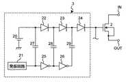
図1は、本発明の第1の実施の形態における逆流防止回路の回路例を示した図である。
図1のスイッチ回路は、入力端INに接続された直流電源10と出力端OUTに接続された負荷11を接続する回路であり、NMOSトランジスタからなるスイッチ2と、スイッチ2にゲート電圧を供給してオンさせるゲート駆動回路3と、負荷11から直流電源10への電流の逆流を防止する逆流防止回路4とで構成されている。逆流防止回路4は、NMOSトランジスタ7及びインバータ8で構成されている。なお、スイッチ2は第1のスイッチを、NMOSトランジスタ7は遮断回路を、インバータ8は論理回路をそれぞれなす。また、NMOSトランジスタ7は第2のスイッチをなす。
逆流防止回路4は、出力端OUTの電圧が入力端INの電圧よりも大きくなり、スイッチ2を介して出力端OUTから入力端INに電流が逆流することを防止する。Next, the present invention will be described in detail based on the embodiments shown in the drawings.
First embodiment.
FIG. 1 is a diagram showing a circuit example of a backflow prevention circuit according to the first embodiment of the present invention.
The switch circuit of FIG. 1 is a circuit that connects a
The
入力端INと出力端OUTとの間にはスイッチ2が接続され、スイッチ2のゲートにはゲート駆動回路3からゲート電圧が供給されている。スイッチ2のサブストレートゲートは出力端OUTに接続され、スイッチ2のゲートと接地電圧との間にNMOSトランジスタ7が接続されている。インバータ8の入力端は入力端INに接続され、インバータ8の出力端はNMOSトランジスタ7のゲートに接続されており、インバータ8は、出力端OUTの電圧を電源にして作動する。NMOSトランジスタ7のサブストレートゲートは接地電圧に接続されている。
インバータ8の内部回路としては、NMOSトランジスタと抵抗、PMOSトランジスタと抵抗、又はNMOSトランジスタとPMOSトランジスタ等の組み合わせを用いることができるが、消費電力を低減させるためにはNMOSトランジスタとPMOSトランジスタの組み合わせを使用する方がよい。A
As an internal circuit of the
ゲート駆動回路3は、例えば、図2で示すようなチャージポンプ回路で構成された昇圧回路をなしている。
図2において、ゲート駆動回路3は、所定の直流電圧を供給する電圧源20、所定の矩形波を生成して出力する発振回路21,ダイオード22〜24,インバータ25,26及びコンデンサ27〜29で構成されている。
電圧源20において、正側電源端子はダイオード22のアノードとコンデンサ27の一端に接続され、コンデンサ27の他端とインバータ25の入力端は発振回路21の出力端に接続されている。ダイオード22のカソードは、ダイオード23のアノードとコンデンサ28の一端にそれぞれ接続され、インバータ25の出力端は、コンデンサ28の他端及びインバータ26の入力端にそれぞれ接続されている。同様に、ダイオード23のカソードは、ダイオード24のアノードとコンデンサ29の一端にそれぞれ接続され、インバータ26の出力端は、コンデンサ29の他端に接続されている。ダイオード24のカソードが、ゲート駆動回路3の出力端をなし、スイッチ2のゲートに接続されている。The
In FIG. 2, the
In the
このような構成において、インバータ8は、出力端OUTの電圧が入力端INの電圧よりも大きくなると、NMOSトランジスタ7のゲートにハイレベルの信号を出力しNMOSトランジスタ7をオンさせる。NMOSトランジスタ7は、オンするとスイッチ2のゲートを接地電圧に接続し、ゲート駆動回路3の動作に関係なくスイッチ2をオフさせて遮断状態にする。このようにして、逆流防止回路4は、出力端OUTから入力端INへの電流の逆流を防止する。また、NMOSトランジスタ7を流れる電流も、スイッチ2が動作していない状態では非常に微小である。スイッチ2が動作している状態でも、わずかにゲート駆動回路3から流れ出る電流のみである。スイッチ2に対するゲート駆動回路3は、図2に示すようなチャージポンプ回路等で構成されるが、通常スイッチ2のゲートには電流が流れないため、ゲート駆動回路3の出力電流は概ね小さくて良い。 In such a configuration, when the voltage at the output terminal OUT becomes larger than the voltage at the input terminal IN, the
このように、本第1の実施の形態における逆流防止回路は、出力端OUTの電圧が入力端INの電圧よりも大きくなると、インバータ8からNMOSトランジスタ7のゲートにハイレベルの信号を出力しNMOSトランジスタ7をオンさせてスイッチ2のゲートを接地電圧に接続して、ゲート駆動回路3の動作に関係なくスイッチ2をオフさせて遮断状態にするようにした。このことから、入力端から出力端に流れる順方向の電流に対する電力損失を増大させることなく、省電力化を図ることができ、1つのインバータと1つのMOSトランジスタで構成することができるため、回路規模が小さく容易に集積化を行うことができる逆流防止回路を得ることができる。 As described above, the backflow prevention circuit according to the first embodiment outputs a high level signal from the
第2の実施の形態.
前記第1の実施の形態では、出力端OUTの電圧が低下した場合、インバータ8の電源電圧が低下することから、インバータ8の出力信号がローレベルになるための入力電圧範囲が狭まる。従って、入力端INの電圧が出力端OUTの電圧よりもわずかに下がっただけで、インバータ8の出力端から出力端OUTの電圧と同程度の電圧が出力され、NMOSトランジスタ7をオンさせる可能性があった。そこで、インバータ8の出力端と接地電圧との間に、プルダウン抵抗の働きをする定電流源を形成したデプレッション型のNMOSトランジスタを設けるようにしてもよく、このようにしたものを本発明の第2の実施の形態とする。
図3は、本発明の第2の実施の形態における逆流防止回路の回路例を示した図である。なお、図3では、図1と同じもの又は同様のものは同じ符号で示し、ここではその説明を省略すると共に図1との相違点のみ説明する。Second embodiment.
In the first embodiment, when the voltage at the output terminal OUT is lowered, the power supply voltage of the
FIG. 3 is a diagram showing a circuit example of a backflow prevention circuit according to the second embodiment of the present invention. In FIG. 3, the same or similar parts as those in FIG. 1 are denoted by the same reference numerals, and description thereof is omitted here, and only differences from FIG. 1 are described.
図3における図1との相違点は、インバータ8の出力端と接地電圧との間に、プルダウン抵抗の働きをする定電流源を形成したデプレッション型NMOSトランジスタ31を設けたことにあり、これに伴って図1の逆流防止回路4を逆流防止回路4aにした。
図3のスイッチ回路は、スイッチ2と、ゲート駆動回路3と、負荷11から直流電源10への電流の逆流を防止する逆流防止回路4aとで構成されている。逆流防止回路4aは、NMOSトランジスタ7、インバータ8及びデプレッション型NMOSトランジスタ31で構成されている。インバータ8の出力端と接地電圧との間にデプレッション型NMOSトランジスタ31が接続され、デプレッション型NMOSトランジスタ31のゲート及びサブストレートゲートはそれぞれ接地電圧に接続されている。3 is different from FIG. 1 in that a depletion
The switch circuit shown in FIG. 3 includes a
このような構成において、デプレッション型NMOSトランジスタ31は、出力端OUTが低電圧である条件下での逆流防止回路の耐ノイズ性を改善させるために付加されており、定電流源を形成してプルダウン抵抗の働きをなしている。このため、デプレッション型NMOSトランジスタ31は、出力端OUTの電圧が低下した場合、インバータ8の電源電圧が低下してインバータ8の出力信号がローレベルになるための入力電圧範囲が狭まり、入力端INの電圧が出力端OUTの電圧よりもわずかに下がっただけで、インバータ8の出力端から出力端OUTの電圧と同程度の電圧が出力されてNMOSトランジスタ7をオンさせることを防止することができる。 In such a configuration, the depletion
図4は、本発明の第2の実施の形態における逆流防止回路の他の回路例を示した図である。なお、図4では、図3と同じもの又は同様のものは同じ符号で示し、ここではその説明を省略すると共に図3との相違点のみ説明する。
図4における図3との相違点は、デプレッション型NMOSトランジスタ31のゲートを入力端INに接続したことにある。このようにすることによっても、図3の場合と同様の効果を得ることができる。FIG. 4 is a diagram showing another circuit example of the backflow prevention circuit according to the second embodiment of the present invention. 4 that are the same as or similar to those in FIG. 3 are denoted by the same reference numerals, and description thereof is omitted here, and only differences from FIG. 3 are described.
4 is different from FIG. 3 in that the gate of the depletion
このように、本第2の実施の形態の逆流防止回路では、前記第1の実施の形態のインバータ8の出力端に、プルダウン抵抗の働きをなすデプレッション型NMOSトランジスタ31を接続するようにした。このことから、前記第1の実施の形態と同様の効果を得ることができると共に、出力端OUTの電圧が低下した場合、インバータ8の電源電圧が低下してインバータ8の出力信号がローレベルになるための入力電圧範囲が狭まり、入力端INの電圧が出力端OUTの電圧よりもわずかに下がっただけで、インバータ8の出力端から出力端OUTの電圧と同程度の電圧が出力されてNMOSトランジスタ7をオンさせることを防止することができる。 As described above, in the backflow prevention circuit of the second embodiment, the depletion
第3の実施の形態.
スイッチ2のサブストレートゲートが接地電圧であると、入力端INに正規の電圧が加わった状態でスイッチ2が導通した場合、スイッチ2のソースとサブストレートゲートとの間に逆バイアスがかかるため、基板バイアス効果によってスイッチ2のしきい値電圧が上昇し、結果的にスイッチ2のオン抵抗が増加してしまう。このようなことを防止するために、前記第1及び第2の各実施の形態では、スイッチ2のサブストレートゲートは出力端OUTと同じ電圧に保たれ、基板バイアス効果の影響を受けないようにしていた。しかし、このようにした場合、逆流状態に陥ると入力端INよりもサブストレートゲートの電圧が大きくなるため、スイッチ2の寄生トランジスタが順バイアス状態になって、電流のリークを引き起こす場合が考えられる。そこで、スイッチ2のサブストレートゲートに対しても逆流状態時における接地回路が必要となり、このようにしたものを本発明の第3の実施の形態とする。Third embodiment.
If the substrate gate of the
図5は、本発明の第3の実施の形態における逆流防止回路の回路例を示した図である。なお、図5では、図3と同じもの又は同様のものは同じ符号で示し、ここではその説明を省略すると共に図3との相違点のみ説明する。
図5における図3との相違点は、逆流状態のときに接地回路をなすNMOSトランジスタ35及び抵抗36を追加したことにある。これに伴って図2の逆流防止回路4aを逆流防止回路4bにした。
図5のスイッチ回路は、スイッチ2と、ゲート駆動回路3と、負荷11から直流電源10への電流の逆流を防止する逆流防止回路4bとで構成されている。逆流防止回路4bは、NMOSトランジスタ7,35、インバータ8、デプレッション型NMOSトランジスタ31及び抵抗36で構成されている。なお、NMOSトランジスタ35は第3のスイッチをなす。スイッチ2のサブストレートゲートは抵抗36を介して出力端OUTに接続され、スイッチ2のサブストレートゲートと接地電圧との間にNMOSトランジスタ35が接続されている。NMOSトランジスタ35のゲートはインバータ8の出力端に接続され、NMOSトランジスタ35のサブストレートゲートは接地電圧に接続されている。FIG. 5 is a diagram showing a circuit example of a backflow prevention circuit according to the third embodiment of the present invention. In FIG. 5, the same or similar elements as those in FIG. 3 are denoted by the same reference numerals, and the description thereof will be omitted here, and only the differences from FIG. 3 will be described.
5 is different from FIG. 3 in that an
The switch circuit of FIG. 5 includes a
このような構成において、出力端OUTから入力端INに電流が逆流する逆流状態になると、インバータ8の出力端はハイレベルの電圧になり、NMOSトランジスタ7がオンすると同時にNMOSトランジスタ35もオンしてスイッチ2のサブストレートゲートを接地電圧にする。この際、抵抗36は、NMOSトランジスタ35がオンした際に、該NMOSトランジスタ35に流れる電流の制限を行う。このため、スイッチ2は完全にオフして遮断状態になり、電流の逆流を防止する。なお、図5では、図3の回路を使用した場合を例にして示したが、図1、図3及び図4の場合も同様であるのでその説明を省略する。また、抵抗36は、逆流状態に陥った際、出力端OUTからNMOSトランジスタ35を介して接地電圧に流れる電流を許容できるだけの大きさがあればよい。 In such a configuration, when the current flows back from the output terminal OUT to the input terminal IN, the output terminal of the
このように、本第3の実施の形態の逆流防止回路では、前記第2の実施の形態のスイッチ2のサブストレートゲートと接地電圧との間にNMOSトランジスタ35を接続すると共に、スイッチ2のサブストレートゲートを抵抗36を介して出力端OUTに接続するようにした。このことから、前記第2の実施の形態と同様の効果を得ることができると共に、逆流が発生した際にスイッチ2のリーク電流をなくすことができ、スイッチ2を完全にオフさせて遮断状態にすることができ、電流の逆流をより完全に遮断することができる。 As described above, in the backflow prevention circuit of the third embodiment, the
なお、前記第3の実施の形態では、図3の回路を使用した場合を例にして示したが、図1及び図4の回路を使用した場合も同様であるのでその説明を省略する。また、第1から第3の各実施の形態において、特に明記していないMOSトランジスタはエンハンスメント型のMOSトランジスタである。また、第1から第3の各実施の形態におけるインバータを構成するMOSトランジスタや、第2及び第3の各実施の形態における耐ノイズ性向上のためのデプレッション型のMOSトランジスタは、最小の面積で形成するようにしても問題はない。 In the third embodiment, the case where the circuit of FIG. 3 is used is shown as an example, but the same applies to the case where the circuits of FIGS. 1 and 4 are used. In each of the first to third embodiments, the MOS transistors not particularly specified are enhancement-type MOS transistors. Further, the MOS transistors constituting the inverters in the first to third embodiments and the depletion type MOS transistors for improving noise resistance in the second and third embodiments have a minimum area. There is no problem even if it is formed.
2 スイッチ
3 ゲート駆動回路
4,4a,4b 逆流防止回路
7,35 NMOSトランジスタ
8 インバータ
10 直流電源
11 負荷
31 デプレッション型NMOSトランジスタ
36 抵抗
2
Claims (11)
Translated fromJapanese前記出力端OUTの電圧を基準にして、前記入力端INの電圧である入力電圧を2値化して出力する論理回路と、
該論理回路の出力信号に応じて前記第1のスイッチの制御電極を所定の電圧に接続して該第1のスイッチを遮断状態にする遮断回路と、
を備え、
前記論理回路は、入力端に前記入力電圧が入力され前記出力電圧を電源とするインバータからなり、前記入力電圧が前記出力端OUTの電圧である出力電圧よりも小さくなると、前記遮断回路に対して、前記第1のスイッチを遮断状態にするための信号を出力することを特徴とする逆流防止回路。In a backflow prevention circuit for preventing a backflow in which a current flows from the output end OUT to the input end IN in a switch circuit that conducts or cuts off a current flow from the input end IN to the output end OUT by a first switch,
A logic circuit that binarizes and outputs an input voltage that is a voltage of the input terminal IN with reference to the voltage of the output terminal OUT;
A blocking circuit for blocking statethe firstswitch in response to the output signal ofthe logic circuitis connected to the control electrode of thefirst switch to a predetermined voltage,
With
The logic circuit includes an inverter that receives the input voltage at an input terminal and uses the output voltage as a power source. When the input voltage becomes smaller than an output voltage that is a voltage of the output terminal OUT, the logic circuitbackflow preventing circuit and outputs the signal to thepre-Symbol first switch off.
前記第1のスイッチのサブストレートゲートと接地電圧との間に接続され、前記論理回路の出力信号に応じて前記第2のスイッチと同じスイッチング動作を行う第3のスイッチと、
を備えることを特徴とする請求項8又は9記載の逆流防止回路。A resistor connected between the substrate gate of thefirst switchand the output terminal OUT;
A third switch connected between the substrate gate of the first switch and a ground voltage and performing the same switching operation as the second switch in response to an output signal of the logic circuit;
Backflow prevention circuit according to claim8, wherein furthercomprising a.
Priority Applications (3)
| Application Number | Priority Date | Filing Date | Title |
|---|---|---|---|
| JP2005355809AJP4597044B2 (en) | 2005-12-09 | 2005-12-09 | Backflow prevention circuit |
| US11/636,308US7423471B2 (en) | 2005-12-09 | 2006-12-07 | Backflow preventing circuit capable of preventing reverse current efficiently |
| US12/177,451US7705657B2 (en) | 2005-12-09 | 2008-07-22 | Backflow preventing circuit capable of preventing reverse current efficiently |
Applications Claiming Priority (1)
| Application Number | Priority Date | Filing Date | Title |
|---|---|---|---|
| JP2005355809AJP4597044B2 (en) | 2005-12-09 | 2005-12-09 | Backflow prevention circuit |
Publications (2)
| Publication Number | Publication Date |
|---|---|
| JP2007166685A JP2007166685A (en) | 2007-06-28 |
| JP4597044B2true JP4597044B2 (en) | 2010-12-15 |
Family
ID=38173149
Family Applications (1)
| Application Number | Title | Priority Date | Filing Date |
|---|---|---|---|
| JP2005355809AExpired - Fee RelatedJP4597044B2 (en) | 2005-12-09 | 2005-12-09 | Backflow prevention circuit |
Country Status (2)
| Country | Link |
|---|---|
| US (2) | US7423471B2 (en) |
| JP (1) | JP4597044B2 (en) |
Families Citing this family (22)
| Publication number | Priority date | Publication date | Assignee | Title |
|---|---|---|---|---|
| EP2070178A2 (en)* | 2006-07-26 | 2009-06-17 | Vijay Jagdish Chheda | An energy source |
| JP2009017648A (en)* | 2007-07-03 | 2009-01-22 | Canon Inc | Charger |
| KR101091352B1 (en)* | 2008-05-28 | 2011-12-07 | 주식회사 엘지화학 | Battery pack balancing device with overdischarge protection |
| JP5219876B2 (en)* | 2009-02-13 | 2013-06-26 | 新日本無線株式会社 | Bias current generator |
| JP5376641B2 (en)* | 2009-02-27 | 2013-12-25 | Necエナジーデバイス株式会社 | Battery device |
| US7990196B2 (en)* | 2009-12-22 | 2011-08-02 | Toshiba America Electronic Components, Inc. | Signal driver with first pulse boost |
| CN102055183B (en)* | 2010-12-09 | 2013-06-05 | 东莞市智维数控科技有限公司 | Electric wheelchair on-off control circuit |
| CN103023116B (en)* | 2012-12-31 | 2015-06-10 | 惠州Tcl移动通信有限公司 | Mobile communication terminal and circuit used for protecting charging of mobile communication terminal |
| CN103683265B (en)* | 2013-12-12 | 2017-02-15 | 安伏(苏州)电子有限公司 | Power source output current direction control and protection device |
| US9705307B2 (en) | 2015-01-27 | 2017-07-11 | Qualcomm Incorporated | Self-sensing reverse current protection switch |
| EP3154191B1 (en)* | 2015-10-09 | 2020-12-30 | The Swatch Group Research and Development Ltd. | Drive circuit for an oscillator |
| US10164425B2 (en)* | 2016-03-29 | 2018-12-25 | Nxp B.V. | Electrostatic discharge protection |
| CN107437888B (en)* | 2016-05-26 | 2019-11-01 | 登丰微电子股份有限公司 | Power switch circuit and applied power supply circuit |
| JP6973247B2 (en)* | 2018-03-30 | 2021-11-24 | ブラザー工業株式会社 | Power supply board and printing equipment |
| CN109379071B (en)* | 2018-12-20 | 2023-09-19 | 上海艾为电子技术股份有限公司 | Analog switch circuit |
| CN110780619B (en)* | 2019-10-14 | 2020-12-25 | 珠海格力电器股份有限公司 | Circuit control method, device and equipment |
| CN210985660U (en)* | 2019-10-24 | 2020-07-10 | 深圳市道通智能航空技术有限公司 | Anti-reverse-filling circuit |
| CN110901396A (en)* | 2019-11-25 | 2020-03-24 | 航天时代飞鸿技术有限公司 | Anti-mutual-charging circuit and method for power supply of multiple battery packs of four-rotor aircraft |
| CN111682869B (en)* | 2020-07-03 | 2024-02-09 | 上海艾为电子技术股份有限公司 | Anti-backflow current load switch and electronic equipment |
| JP7352524B2 (en) | 2020-07-29 | 2023-09-28 | 株式会社東芝 | driver circuit |
| US12026028B2 (en) | 2021-10-22 | 2024-07-02 | Shaoxing Yuanfang Semiconductor Co., Ltd. | Preventing reverse-current flow when an integrated circuit operates using power supplies of different magnitudes |
| CN115328247B (en)* | 2022-08-16 | 2023-11-24 | 骏盈半导体(上海)有限公司 | Power supply module and voltage stabilizing circuit |
Family Cites Families (14)
| Publication number | Priority date | Publication date | Assignee | Title |
|---|---|---|---|---|
| JPS58144234A (en) | 1982-02-20 | 1983-08-27 | Ricoh Co Ltd | power supply |
| JPH03238365A (en)* | 1990-02-15 | 1991-10-24 | Nec Corp | Low voltage detection circuit |
| JP3329168B2 (en) | 1995-01-13 | 2002-09-30 | オムロン株式会社 | Backflow prevention device |
| JP3210567B2 (en) | 1996-03-08 | 2001-09-17 | 株式会社東芝 | Semiconductor output circuit |
| JPH10240359A (en) | 1997-03-03 | 1998-09-11 | Oki Electric Ind Co Ltd | Check circuit |
| JPH114157A (en)* | 1997-06-12 | 1999-01-06 | Matsushita Electric Ind Co Ltd | Semiconductor integrated circuit |
| JP4080043B2 (en) | 1997-12-24 | 2008-04-23 | 株式会社ルネサステクノロジ | Booster circuit, semiconductor memory device, and data processing device |
| JP2000201429A (en) | 1998-09-08 | 2000-07-18 | Ricoh Co Ltd | Overvoltage protection circuit |
| JP2001051730A (en)* | 1999-08-05 | 2001-02-23 | Fujitsu Ltd | Switch circuit and series regulator |
| US6225857B1 (en)* | 2000-02-08 | 2001-05-01 | Analog Devices, Inc. | Non-inverting driver circuit for low-dropout voltage regulator |
| JP2002152978A (en) | 2000-11-08 | 2002-05-24 | Nichicon Corp | Reverse-current preventing circuit |
| JP2002152968A (en)* | 2000-11-10 | 2002-05-24 | Fujitsu Ltd | Backflow prevention circuit |
| JP2003258614A (en) | 2002-02-28 | 2003-09-12 | Matsushita Electric Ind Co Ltd | Analog switch circuit with backflow prevention function |
| JP2005151677A (en)* | 2003-11-14 | 2005-06-09 | Omron Corp | Additional power supply equipment |
- 2005
- 2005-12-09JPJP2005355809Apatent/JP4597044B2/ennot_activeExpired - Fee Related
- 2006
- 2006-12-07USUS11/636,308patent/US7423471B2/ennot_activeExpired - Fee Related
- 2008
- 2008-07-22USUS12/177,451patent/US7705657B2/ennot_activeExpired - Fee Related
Also Published As
| Publication number | Publication date |
|---|---|
| US20080285191A1 (en) | 2008-11-20 |
| JP2007166685A (en) | 2007-06-28 |
| US20070139836A1 (en) | 2007-06-21 |
| US7423471B2 (en) | 2008-09-09 |
| US7705657B2 (en) | 2010-04-27 |
Similar Documents
| Publication | Publication Date | Title |
|---|---|---|
| JP4597044B2 (en) | Backflow prevention circuit | |
| JP5067786B2 (en) | Power semiconductor device | |
| JP5519052B2 (en) | Load drive device | |
| US8531170B2 (en) | Semiconductor device | |
| US7034573B1 (en) | Level shifter without DC current flow | |
| JP2014207412A (en) | ESD protection circuit | |
| US20120313686A1 (en) | Level shift circuit | |
| JP2007181084A (en) | Switch circuit, diode | |
| JP4285036B2 (en) | Power supply backflow prevention circuit | |
| JP5266030B2 (en) | Load drive device | |
| JP2012203528A (en) | Voltage regulator | |
| US20060232318A1 (en) | Power clamp circuit and semiconductor device | |
| CN212305284U (en) | Substrate potential selection circuit for PMOS (P-channel metal oxide semiconductor) transistor | |
| JP2014206861A (en) | Regulator circuit and semiconductor integrated circuit device in which regulator is formed | |
| JP5005970B2 (en) | Voltage control circuit and semiconductor integrated circuit having voltage control circuit | |
| JP2010028522A (en) | Semiconductor device | |
| CN112543021B (en) | Input-output circuit and circuit system | |
| WO2015114923A1 (en) | Semiconductor integrated circuit device | |
| US9425793B2 (en) | Circuit for generating bias voltage for high speed input/output pad | |
| KR102845796B1 (en) | Delay circuit | |
| JP2017147560A (en) | Level shift circuit | |
| JP6277151B2 (en) | Sensor device | |
| JP6332601B2 (en) | Semiconductor integrated circuit device | |
| JP4794782B2 (en) | Voltage detection circuit and electronic device | |
| JP2005224088A (en) | Load protection circuit |
Legal Events
| Date | Code | Title | Description |
|---|---|---|---|
| RD03 | Notification of appointment of power of attorney | Free format text:JAPANESE INTERMEDIATE CODE: A7423 Effective date:20080131 | |
| A621 | Written request for application examination | Free format text:JAPANESE INTERMEDIATE CODE: A621 Effective date:20080919 | |
| A977 | Report on retrieval | Free format text:JAPANESE INTERMEDIATE CODE: A971007 Effective date:20100430 | |
| A131 | Notification of reasons for refusal | Free format text:JAPANESE INTERMEDIATE CODE: A131 Effective date:20100511 | |
| A521 | Request for written amendment filed | Free format text:JAPANESE INTERMEDIATE CODE: A523 Effective date:20100616 | |
| A131 | Notification of reasons for refusal | Free format text:JAPANESE INTERMEDIATE CODE: A131 Effective date:20100706 | |
| A521 | Request for written amendment filed | Free format text:JAPANESE INTERMEDIATE CODE: A523 Effective date:20100803 | |
| TRDD | Decision of grant or rejection written | ||
| A01 | Written decision to grant a patent or to grant a registration (utility model) | Free format text:JAPANESE INTERMEDIATE CODE: A01 Effective date:20100914 | |
| A01 | Written decision to grant a patent or to grant a registration (utility model) | Free format text:JAPANESE INTERMEDIATE CODE: A01 | |
| A61 | First payment of annual fees (during grant procedure) | Free format text:JAPANESE INTERMEDIATE CODE: A61 Effective date:20100921 | |
| R150 | Certificate of patent or registration of utility model | Free format text:JAPANESE INTERMEDIATE CODE: R150 | |
| FPAY | Renewal fee payment (event date is renewal date of database) | Free format text:PAYMENT UNTIL: 20131001 Year of fee payment:3 | |
| S111 | Request for change of ownership or part of ownership | Free format text:JAPANESE INTERMEDIATE CODE: R313111 | |
| R350 | Written notification of registration of transfer | Free format text:JAPANESE INTERMEDIATE CODE: R350 | |
| R250 | Receipt of annual fees | Free format text:JAPANESE INTERMEDIATE CODE: R250 | |
| LAPS | Cancellation because of no payment of annual fees |