JP4595665B2 - Wiring board manufacturing method - Google Patents
Wiring board manufacturing methodDownload PDFInfo
- Publication number
- JP4595665B2 JP4595665B2JP2005140498AJP2005140498AJP4595665B2JP 4595665 B2JP4595665 B2JP 4595665B2JP 2005140498 AJP2005140498 AJP 2005140498AJP 2005140498 AJP2005140498 AJP 2005140498AJP 4595665 B2JP4595665 B2JP 4595665B2
- Authority
- JP
- Japan
- Prior art keywords
- circuit pattern
- wiring board
- metal
- pattern
- power semiconductor
- Prior art date
- Legal status (The legal status is an assumption and is not a legal conclusion. Google has not performed a legal analysis and makes no representation as to the accuracy of the status listed.)
- Expired - Fee Related
Links
Images


Classifications
- H—ELECTRICITY
- H05—ELECTRIC TECHNIQUES NOT OTHERWISE PROVIDED FOR
- H05K—PRINTED CIRCUITS; CASINGS OR CONSTRUCTIONAL DETAILS OF ELECTRIC APPARATUS; MANUFACTURE OF ASSEMBLAGES OF ELECTRICAL COMPONENTS
- H05K3/00—Apparatus or processes for manufacturing printed circuits
- H05K3/22—Secondary treatment of printed circuits
- H05K3/24—Reinforcing the conductive pattern
- H—ELECTRICITY
- H01—ELECTRIC ELEMENTS
- H01L—SEMICONDUCTOR DEVICES NOT COVERED BY CLASS H10
- H01L23/00—Details of semiconductor or other solid state devices
- H01L23/34—Arrangements for cooling, heating, ventilating or temperature compensation ; Temperature sensing arrangements
- H01L23/36—Selection of materials, or shaping, to facilitate cooling or heating, e.g. heatsinks
- H01L23/373—Cooling facilitated by selection of materials for the device or materials for thermal expansion adaptation, e.g. carbon
- H01L23/3735—Laminates or multilayers, e.g. direct bond copper ceramic substrates
- H—ELECTRICITY
- H01—ELECTRIC ELEMENTS
- H01L—SEMICONDUCTOR DEVICES NOT COVERED BY CLASS H10
- H01L2224/00—Indexing scheme for arrangements for connecting or disconnecting semiconductor or solid-state bodies and methods related thereto as covered by H01L24/00
- H01L2224/01—Means for bonding being attached to, or being formed on, the surface to be connected, e.g. chip-to-package, die-attach, "first-level" interconnects; Manufacturing methods related thereto
- H01L2224/42—Wire connectors; Manufacturing methods related thereto
- H01L2224/44—Structure, shape, material or disposition of the wire connectors prior to the connecting process
- H01L2224/45—Structure, shape, material or disposition of the wire connectors prior to the connecting process of an individual wire connector
- H01L2224/45001—Core members of the connector
- H01L2224/45099—Material
- H01L2224/451—Material with a principal constituent of the material being a metal or a metalloid, e.g. boron (B), silicon (Si), germanium (Ge), arsenic (As), antimony (Sb), tellurium (Te) and polonium (Po), and alloys thereof
- H01L2224/45117—Material with a principal constituent of the material being a metal or a metalloid, e.g. boron (B), silicon (Si), germanium (Ge), arsenic (As), antimony (Sb), tellurium (Te) and polonium (Po), and alloys thereof the principal constituent melting at a temperature of greater than or equal to 400°C and less than 950°C
- H01L2224/45124—Aluminium (Al) as principal constituent
- H—ELECTRICITY
- H01—ELECTRIC ELEMENTS
- H01L—SEMICONDUCTOR DEVICES NOT COVERED BY CLASS H10
- H01L2224/00—Indexing scheme for arrangements for connecting or disconnecting semiconductor or solid-state bodies and methods related thereto as covered by H01L24/00
- H01L2224/01—Means for bonding being attached to, or being formed on, the surface to be connected, e.g. chip-to-package, die-attach, "first-level" interconnects; Manufacturing methods related thereto
- H01L2224/42—Wire connectors; Manufacturing methods related thereto
- H01L2224/47—Structure, shape, material or disposition of the wire connectors after the connecting process
- H01L2224/48—Structure, shape, material or disposition of the wire connectors after the connecting process of an individual wire connector
- H01L2224/4805—Shape
- H01L2224/4809—Loop shape
- H01L2224/48091—Arched
- H—ELECTRICITY
- H01—ELECTRIC ELEMENTS
- H01L—SEMICONDUCTOR DEVICES NOT COVERED BY CLASS H10
- H01L2924/00—Indexing scheme for arrangements or methods for connecting or disconnecting semiconductor or solid-state bodies as covered by H01L24/00
- H01L2924/10—Details of semiconductor or other solid state devices to be connected
- H01L2924/11—Device type
- H01L2924/13—Discrete devices, e.g. 3 terminal devices
- H01L2924/1304—Transistor
- H01L2924/1305—Bipolar Junction Transistor [BJT]
- H01L2924/13055—Insulated gate bipolar transistor [IGBT]
- H—ELECTRICITY
- H01—ELECTRIC ELEMENTS
- H01L—SEMICONDUCTOR DEVICES NOT COVERED BY CLASS H10
- H01L2924/00—Indexing scheme for arrangements or methods for connecting or disconnecting semiconductor or solid-state bodies as covered by H01L24/00
- H01L2924/30—Technical effects
- H01L2924/301—Electrical effects
- H01L2924/3011—Impedance
- H—ELECTRICITY
- H05—ELECTRIC TECHNIQUES NOT OTHERWISE PROVIDED FOR
- H05K—PRINTED CIRCUITS; CASINGS OR CONSTRUCTIONAL DETAILS OF ELECTRIC APPARATUS; MANUFACTURE OF ASSEMBLAGES OF ELECTRICAL COMPONENTS
- H05K1/00—Printed circuits
- H05K1/02—Details
- H05K1/0201—Thermal arrangements, e.g. for cooling, heating or preventing overheating
- H05K1/0203—Cooling of mounted components
- H—ELECTRICITY
- H05—ELECTRIC TECHNIQUES NOT OTHERWISE PROVIDED FOR
- H05K—PRINTED CIRCUITS; CASINGS OR CONSTRUCTIONAL DETAILS OF ELECTRIC APPARATUS; MANUFACTURE OF ASSEMBLAGES OF ELECTRICAL COMPONENTS
- H05K1/00—Printed circuits
- H05K1/02—Details
- H05K1/0213—Electrical arrangements not otherwise provided for
- H05K1/0263—High current adaptations, e.g. printed high current conductors or using auxiliary non-printed means; Fine and coarse circuit patterns on one circuit board
- H—ELECTRICITY
- H05—ELECTRIC TECHNIQUES NOT OTHERWISE PROVIDED FOR
- H05K—PRINTED CIRCUITS; CASINGS OR CONSTRUCTIONAL DETAILS OF ELECTRIC APPARATUS; MANUFACTURE OF ASSEMBLAGES OF ELECTRICAL COMPONENTS
- H05K1/00—Printed circuits
- H05K1/02—Details
- H05K1/03—Use of materials for the substrate
- H05K1/0306—Inorganic insulating substrates, e.g. ceramic, glass
- H—ELECTRICITY
- H05—ELECTRIC TECHNIQUES NOT OTHERWISE PROVIDED FOR
- H05K—PRINTED CIRCUITS; CASINGS OR CONSTRUCTIONAL DETAILS OF ELECTRIC APPARATUS; MANUFACTURE OF ASSEMBLAGES OF ELECTRICAL COMPONENTS
- H05K1/00—Printed circuits
- H05K1/02—Details
- H05K1/03—Use of materials for the substrate
- H05K1/05—Insulated conductive substrates, e.g. insulated metal substrate
- H05K1/056—Insulated conductive substrates, e.g. insulated metal substrate the metal substrate being covered by an organic insulating layer
- H—ELECTRICITY
- H05—ELECTRIC TECHNIQUES NOT OTHERWISE PROVIDED FOR
- H05K—PRINTED CIRCUITS; CASINGS OR CONSTRUCTIONAL DETAILS OF ELECTRIC APPARATUS; MANUFACTURE OF ASSEMBLAGES OF ELECTRICAL COMPONENTS
- H05K2203/00—Indexing scheme relating to apparatus or processes for manufacturing printed circuits covered by H05K3/00
- H05K2203/13—Moulding and encapsulation; Deposition techniques; Protective layers
- H05K2203/1333—Deposition techniques, e.g. coating
- H05K2203/1344—Spraying small metal particles or droplets of molten metal
- Y—GENERAL TAGGING OF NEW TECHNOLOGICAL DEVELOPMENTS; GENERAL TAGGING OF CROSS-SECTIONAL TECHNOLOGIES SPANNING OVER SEVERAL SECTIONS OF THE IPC; TECHNICAL SUBJECTS COVERED BY FORMER USPC CROSS-REFERENCE ART COLLECTIONS [XRACs] AND DIGESTS
- Y10—TECHNICAL SUBJECTS COVERED BY FORMER USPC
- Y10T—TECHNICAL SUBJECTS COVERED BY FORMER US CLASSIFICATION
- Y10T29/00—Metal working
- Y10T29/49—Method of mechanical manufacture
- Y10T29/49002—Electrical device making
- Y10T29/49117—Conductor or circuit manufacturing
- Y10T29/49124—On flat or curved insulated base, e.g., printed circuit, etc.
- Y10T29/4913—Assembling to base an electrical component, e.g., capacitor, etc.
- Y—GENERAL TAGGING OF NEW TECHNOLOGICAL DEVELOPMENTS; GENERAL TAGGING OF CROSS-SECTIONAL TECHNOLOGIES SPANNING OVER SEVERAL SECTIONS OF THE IPC; TECHNICAL SUBJECTS COVERED BY FORMER USPC CROSS-REFERENCE ART COLLECTIONS [XRACs] AND DIGESTS
- Y10—TECHNICAL SUBJECTS COVERED BY FORMER USPC
- Y10T—TECHNICAL SUBJECTS COVERED BY FORMER US CLASSIFICATION
- Y10T29/00—Metal working
- Y10T29/49—Method of mechanical manufacture
- Y10T29/49002—Electrical device making
- Y10T29/49117—Conductor or circuit manufacturing
- Y10T29/49124—On flat or curved insulated base, e.g., printed circuit, etc.
- Y10T29/49155—Manufacturing circuit on or in base
Landscapes
- Engineering & Computer Science (AREA)
- Chemical & Material Sciences (AREA)
- Microelectronics & Electronic Packaging (AREA)
- Physics & Mathematics (AREA)
- Manufacturing & Machinery (AREA)
- Condensed Matter Physics & Semiconductors (AREA)
- General Physics & Mathematics (AREA)
- Computer Hardware Design (AREA)
- Ceramic Engineering (AREA)
- Power Engineering (AREA)
- Materials Engineering (AREA)
- Insulated Metal Substrates For Printed Circuits (AREA)
- Manufacturing Of Printed Wiring (AREA)
- Cooling Or The Like Of Semiconductors Or Solid State Devices (AREA)
- Parts Printed On Printed Circuit Boards (AREA)
- Other Surface Treatments For Metallic Materials (AREA)
- Structure Of Printed Boards (AREA)
Description
Translated fromJapanese本発明は配線基板の製造方法に関し、特に放熱性に優れ、産業用の電源機器にも適用できる配線基板の製造方法に関する。The present invention relates to amethod of manufacturing a wiring board, particularly excellent heat dissipation, amanufacturing method of the wiring substrate can be applied to the power supply equipment for industry.
電源装置に使用される半導体モジュールは、家庭用エアコン、冷蔵庫などの民生機器から、インバータ、サーボコントローラなどの産業機器まで、広範囲に渡って適用されている。特に、パワー半導体を搭載したIGBT(Insulated Gate Bipolar Transistor)モジュールなどは、発熱が大きいことから、放熱性に優れた金属ベース配線基板やセラミックス配線基板が用いられてきている。 Semiconductor modules used for power supply devices are applied in a wide range from consumer equipment such as home air conditioners and refrigerators to industrial equipment such as inverters and servo controllers. In particular, an IGBT (Insulated Gate Bipolar Transistor) module equipped with a power semiconductor generates a large amount of heat, so that a metal base wiring board or a ceramic wiring board having excellent heat dissipation has been used.
図3は従来の金属ベース配線基板の断面構造を示す図である。
金属ベース配線基板は、ベース金属101と、このベース金属101上に形成された絶縁層102と、この絶縁層102上に形成された回路パターン103との3層構造になっている。ベース金属101は、アルミニウム板または銅板などの放熱性に優れた金属が用いられている。絶縁層102は、SiO2,Al2O3,AlNなどの無機フィラーを含有したエポキシ樹脂などからなっている。FIG. 3 is a view showing a cross-sectional structure of a conventional metal base wiring board.
The metal base wiring board has a three-layer structure of a
回路パターン103は、通常、銅箔が用いられているが、まれにアルミ箔が用いられる場合もある。銅箔は、通常35μm〜140μm程度の厚みのものが用いられている。この銅箔は、湿式エッチングにより所定の回路パターンに加工される。電流容量が10A程度と小さく、発熱の小さいパワー半導体の場合、そのパワー半導体は、直接この回路パターン103にはんだ付け接合により搭載される。パワー半導体の電流容量が大きくなる場合は、熱をこの回路パターン103上に広げて熱抵抗を低減させるため、銅箔の厚みは、140μm程度の厚いものにする。140μmで足りない場合は、さらに厚い、例えば200μm、250μmなどの銅箔を用いる。さらに、回路パターン103の厚みを1mm以上、例えば3〜4mmの厚みにすれば、ヒートスプレッダ効果が発揮され、パワー半導体で発生した熱は横方向に広がり、熱抵抗は大幅に低減される。 The
金属ベース配線基板に使用される絶縁層102は、絶縁信頼性と熱放散性に優れていることが必要である。さらに、絶縁層102としては、応力緩和性、耐湿性、耐熱性などに優れていることも要求されており、それに適した樹脂組成物も知られている(たとえば、特許文献1〜3参照。)。このように、回路パターン103が熱放散性に優れた絶縁層102を介してベース金属101に接合されていることにより、金属ベース配線基板は、パワー半導体など高発熱部品を実装する配線基板として用いられている。 The
しかしながら、SiO2,Al2O3,AlNなどの無機フィラーを含有したエポキシ樹脂の場合、充填量に限界があるので、その熱伝導率は現状7〜10W/m・K程度である。したがって、適用できるパワー半導体モジュールの電流容量にも限界があり、現状では50Aクラス程度までしか適用できない。However, in the case of an epoxy resin containing an inorganic filler such as SiO2 , Al2 O3 , AlN, etc., since the filling amount is limited, its thermal conductivity is currently about 7 to 10 W / m · K. Therefore, there is a limit to the current capacity of the power semiconductor module that can be applied, and at present, it can only be applied up to about 50 A class.
これに対し、50Aを超える、より大容量のパワー半導体モジュールの場合には、金属ベース配線基板ではなく、絶縁層の熱伝導率がより高いセラミックス配線基板が用いられている。 On the other hand, in the case of a power semiconductor module with a larger capacity exceeding 50 A, a ceramic wiring board having a higher thermal conductivity of the insulating layer is used instead of a metal-based wiring board.
図4は従来のセラミックス配線基板の断面構造を示す図であって、(a)はセラミックス配線基板を示し、(b)はベース金属が接合されたセラミックス配線基板を示している。 4A and 4B are diagrams showing a cross-sectional structure of a conventional ceramic wiring board, in which FIG. 4A shows a ceramic wiring board and FIG. 4B shows a ceramic wiring board to which a base metal is bonded.
セラミックス配線基板は、セラミックス絶縁板104の両側に回路パターン103が張り合わせられることによって構成されている。セラミックス絶縁板104は、原料紛をバインダーと練り合せ、グリーンシートと呼ばれるシート状の絶縁板にし、これを高温にて焼成することによって作製される。その後に、回路パターン103用の銅箔、もしくはアルミニム箔を高温で接合することにより、配線基板にする。さらに、これらセラミックス配線基板は、通常、厚さ2〜3mm程度の銅板のベース金属101にはんだ層105を介して接合されている。 The ceramic wiring board is configured by pasting
セラミックス絶縁板104は、その原料として、Al2O3,AlN,Si3N4などが用いられている。そのセラミックス絶縁板104の熱伝導率は、原料がAl2O3の場合、約20W/m・K、原料がAlNの場合、160〜180W/m・K、そして、原料がSi3N4の場合、80W/m・K程度となっており、エポキシ樹脂に無機フィラーを配合した場合に比べて、1〜2桁高くなっている。
しかしながら、金属ベース配線基板の場合、熱抵抗を低減するため、銅箔を厚くしていくと、回路パターン層を加工するためのエッチング加工の時間が厚みに比例して長くなっていくので、加工費が大幅に高くなり、コストが大幅に嵩んでしまうという問題点があった。しかも、回路パターン層の厚みが3〜4mmにもなれば、銅を溶かすのに長い時間を要するだけでなく、回路パターン層の端部のエッチングが精度良くできなくなるので、エッチング加工自体が現実的でなくなる。 However, in the case of a metal-based wiring board, if the copper foil is thickened to reduce the thermal resistance, the etching time for processing the circuit pattern layer becomes longer in proportion to the thickness. There is a problem that the cost is significantly increased and the cost is significantly increased. Moreover, if the thickness of the circuit pattern layer is 3 to 4 mm, not only will it take a long time to melt copper, but the etching of the edge of the circuit pattern layer cannot be performed with high accuracy, so the etching process itself is realistic. Not.
また、セラミックス配線基板の場合、セラミックス絶縁板を一度作製し、それに回路パターン層を接合し、エッチング加工し、このようにして作製されたセラミックス配線基板をベース金属にはんだで接合する、というように多くの工数が必要になっていることから、価格が高く、低価格化が困難であるという問題点があった。しかも、セラミックス配線基板の場合、回路パターン用の銅箔をあまり厚くすることができない。ヒートスプレッダ効果を高めるために厚い銅箔もしくは銅板を貼り付ければよいが、約1000℃以上の高温で銅板をセラミックス絶縁板に接合するので、両側の厚みを同じにしておかないと熱膨張係数の違いにより冷却時にバイメタル効果でそり曲がってしまう。また、前述のように、銅箔または銅板が厚くなるとエッチング加工費が大幅に高くなってしまうので、現在、セラミックス配線基板の回路パターンの厚みは、正確には0.6mm程度以下までしか用いられていない。 In the case of a ceramic wiring board, a ceramic insulating board is manufactured once, a circuit pattern layer is bonded thereto, etching is performed, and the ceramic wiring board thus manufactured is bonded to a base metal by soldering, etc. Since many man-hours are required, there is a problem that the price is high and it is difficult to reduce the price. Moreover, in the case of a ceramic wiring board, the copper foil for the circuit pattern cannot be made too thick. To increase the heat spreader effect, a thick copper foil or copper plate may be attached, but the copper plate is bonded to the ceramic insulating plate at a high temperature of about 1000 ° C or higher. Will bend due to bimetal effect during cooling. Further, as described above, since the etching cost increases significantly when the copper foil or the copper plate becomes thicker, the thickness of the circuit pattern of the ceramic wiring board is currently only used to about 0.6 mm or less. Not.
本発明はこのような点に鑑みてなされたものであり、少ない工数で製造が可能で安価かつ放熱性に優れた配線基板の製造方法を提供することを目的とする。The present invention has been made in view of these points, and an object of the present invention is to provide amethod of manufacturing a wiring board that can be manufactured with a small number of man-hours, is inexpensive, and has excellent heat dissipation.
本発明では上記問題を解決するために、絶縁板に金属箔を張り合わせ、その金属箔を加工して回路パターンを形成した配線基板の製造方法において、発熱半導体部品が搭載される部分の回路パターンの上部に上積み回路パターンを備えたことを特徴とし、その上積み回路パターンは、回路パターンの上部に金属材料をコールドスプレー法により積層して搭載される半導体チップの端部から上積み回路パターンの端部までの距離が回路パターンおよび上積み回路パターンの合計の厚みと等しくなるまで、または、搭載される半導体チップの端部から上積み回路パターンの端部までの距離と回路パターンおよび上積み回路パターンの合計の厚みとの比が0.8〜1.2の範囲になるまで厚みを上積みすることによって形成した。In the present invention, in order to solve the above problem, in amethod of manufacturing a wiring board in which a metal foil is bonded to an insulating plate and the metal foil is processed to form a circuit pattern, the circuit pattern of the portion where the heat generating semiconductor component is mounted It is characterized by having an upper circuit pattern on the upper part, and the upper circuit pattern is from the end of the semiconductor chip mounted by stacking a metal material on the upper part of the circuit pattern by the cold spray method to the end of the upper circuit pattern. Until the total distance of the circuit pattern and the upper circuit pattern is equal to the total thickness of the circuit pattern and the upper circuit pattern, or the distance from the end of the mounted semiconductor chip to the end of the upper circuit pattern and the total thickness of the circuit pattern and the upper circuit pattern It was formed by stacking the thickness until the ratio was in the range of 0.8 to 1.2.
このような配線基板の製造方法によれば、金属箔の回路パターンの上にさらに厚い上積み金属パターンが形成されている。これにより、この厚肉の上積み回路パターン上にパワー半導体を搭載すれば、その損失により発生した熱が厚肉の上積み回路パターンで拡散できるので熱抵抗を減らすことができ、熱抵抗の少ない放熱性に優れた配線基板を構成することができる。According to such amethod of manufacturing a wiring board,a thicker stacked metal pattern is formed on the circuit pattern of the metal foil. As a result, if a power semiconductor is mounted on this thick stacked circuit pattern, the heat generated by the loss can be diffused in the thick stacked circuit pattern, so that the thermal resistance can be reduced, and the heat dissipation with low thermal resistance. An excellent wiring board can be configured.
本発明の配線基板の製造方法は、金属箔の回路パターンを少なくとも部分的に厚く形成することができるため、この厚肉の回路パターン上にパワー半導体を搭載すれば、損失により発生した熱が厚肉の回路パターンで拡散できるので、熱抵抗を減らすことができ、従来の金属ベース配線基板やセラミックス配線基板に比べ大幅に熱抵抗の少ない放熱性に優れた配線基板を安価かつ容易に作製できるという利点がある。
The wiring boardmanufacturing method ofthe present invention can form a metal foil circuit pattern at least partially thick, so if a power semiconductor is mounted on this thick circuit pattern, the heat generated by the loss is thick. Because it can be diffused with a meaty circuit pattern, thermal resistance can be reduced, and it is possible to inexpensively and easily produce a wiring board with significantly less heat resistance and superior heat dissipation than conventional metal-based wiring boards and ceramic wiring boards. There are advantages.
以下、本発明の実施の形態として、絶縁層に金属箔を張り合わせ、その金属箔を加工して所定の回路パターンを形成した金属ベースのプリント配線板に適用した場合を例に図面を参照して詳細に説明する。 Hereinafter, as an embodiment of the present invention, with reference to the drawings, an example in which the present invention is applied to a metal-based printed wiring board in which a predetermined circuit pattern is formed by bonding a metal foil to an insulating layer and processing the metal foil. This will be described in detail.
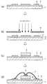
図1は本発明の配線基板の製造工程および完成したパワー半導体モジュールの状態を示したものであって、(a)は金属ベース配線基板を示し、(b)はコールドスプレーによる上積み回路パターンの形成工程を示し、(c)は上積み回路パターンが形成された状態を示し、(d)は上積み回路パターン上にパワー半導体が実装されたパワー半導体モジュールを示している。 FIG. 1 shows a manufacturing process of a wiring board according to the present invention and a state of a completed power semiconductor module, wherein (a) shows a metal-based wiring board, and (b) shows the formation of an overlaid circuit pattern by cold spraying. (C) shows a state in which an overlaid circuit pattern is formed, and (d) shows a power semiconductor module in which a power semiconductor is mounted on the overlaid circuit pattern.
金属ベース配線基板は、図1の(a)に示したように、ベース金属1上に無機フィラーを含有した絶縁層2を設け、その上に回路パターン3を張り合わせた3層構造の構成になっている。 As shown in FIG. 1A, the metal base wiring board has a three-layer structure in which an
回路パターン3は、通常、銅箔が用いられている。なお、この回路パターン3は、銅箔に代えて、アルミ箔を用いてもよい。絶縁層2に張り合わされた銅箔は、湿式エッチングにより所定のパターンに加工され、回路パターン3となる。ここで、銅箔は、通常、35μm〜140μm程度の厚みを持った標準品が用いられる。また、回路パターン3のパターン幅は、回路の電流容量により決められるが、エッチング加工費を考慮すると、銅箔の厚さは、できるだけ薄い方が望ましい。 The
以上のように形成された金属ベース配線基板は、従来の金属ベース配線基板と同じであるが、本発明による配線基板では、回路パターン3の中で、放熱性を向上させたい領域のみ部分的に厚みを増すようにしている。すなわち、図1の(b)に示したように、回路パターン3の上に、その厚みを増したい領域に対応した形状の孔が開けられたマスク4を配置し、その上方からコールドスプレー法にて金属紛を常温にて超音速で吹き付け、回路パターン3上に金属紛を積層させていくことにより、図1の(c)に示した上積み回路パターン5を形成する。 The metal base wiring board formed as described above is the same as the conventional metal base wiring board. However, in the wiring board according to the present invention, only a region in the
ここで、コールドスプレー法について説明する。コールドスプレー法は、溶射技術の1つとしてとらえられており、溶射材料の融点または軟化温度よりも低い温度のガスを超音速流にして、その流れの中に溶射材料粒子を投入して加速させ、固相状態のまま基材に高速で衝突させて皮膜を形成する技術である。コールドスプレー法の特徴は、従来のプラズマ溶射法、フレーム溶射法、高速フレーム溶射法などに比べて、溶射材料粒子を加熱・加速する作動ガスの温度が著しく低いことである。プラズマ溶射などは2000〜8000℃の高い作動ガスの温度が必要であるが、コールドスプレーの場合、常温〜600℃程度の作動ガスでよい。溶射材料粒子をあまり加熱せずに固相状態のまま基材へ高速で衝突させるが、臨界速度に達するとその衝突エネルギにより基材と溶射材料粒子とが塑性変形して皮膜を形成する。そのため、他の溶射方法と違い、溶射材料の熱による酸化や熱変質を最小限にすることが可能である。 Here, the cold spray method will be described. The cold spray method is regarded as one of the thermal spraying techniques. A gas having a temperature lower than the melting point or softening temperature of the thermal spray material is converted into a supersonic flow, and the thermal spray material particles are injected into the flow to accelerate. This is a technique for forming a film by colliding with a substrate at a high speed in a solid state. The feature of the cold spray method is that the temperature of the working gas for heating and accelerating the sprayed material particles is significantly lower than that of the conventional plasma spraying method, flame spraying method, high-speed flame spraying method and the like. Plasma spraying or the like requires a high working gas temperature of 2000 to 8000 ° C, but in the case of cold spray, a working gas of room temperature to about 600 ° C may be used. The thermal spray material particles are allowed to collide with the base material at a high speed in a solid state without being heated so much, but when the critical velocity is reached, the base material and the thermal spray material particles are plastically deformed to form a film. Therefore, unlike other thermal spraying methods, it is possible to minimize oxidation and thermal alteration of the thermal spray material due to heat.
コールドスプレー装置は、ボンベなどのガス源から供給された高圧ガスを粉末供給装置とガス加熱器とに分岐させる。このうち、主流の作動ガスは、電気炉などで直接または間接的に加熱されるコイル状のガス管内を流れて温度が上げられ、溶射ガンに供給されて超音速ノズルにより加速されて噴出する。 The cold spray device branches high-pressure gas supplied from a gas source such as a cylinder into a powder supply device and a gas heater. Of these, the mainstream working gas flows through a coiled gas pipe heated directly or indirectly by an electric furnace or the like, is heated, is supplied to a spray gun, is accelerated by a supersonic nozzle, and is ejected.
一方、作動ガスの一部は、粉末供給装置へ分流されてキャリアガスとして溶射粉末とともに溶射ガン後方に流入される。作動ガスの加熱は、行なわない場合もあるが、加熱した方が粒子速度を高くでき、かつ粒子の塑性変形を生じやすくするために有利である。ガスとしては空気、ヘリウム、窒素が使用される。 On the other hand, a part of the working gas is diverted to the powder supply device and flows into the back of the spray gun together with the spray powder as a carrier gas. Although the heating of the working gas may not be performed, the heating is advantageous in that it can increase the particle velocity and easily cause plastic deformation of the particles. Air, helium, or nitrogen is used as the gas.
ここで、回路パターン3に溶射される溶射材料には、粒子径が1〜50μmの金属材料が用いられる。その粒子材料としては、銅、アルミニウム、鉄、チタン、モリブデン、ニッケルなどが用いられる。配線基板用には、通常、銅またはアルミニウムが用いられる。これらの溶射材料粒子は、500〜900m/sのスピードで、10〜50mmの距離を隔ててマスク4越しに回路パターン3に吹き付けられて堆積させられ、これによって、図1の(c)に示したように、回路パターン3上に上積み回路パターン5が形成される。上積み回路パターン5が必要な膜厚を得るため、溶射材料粒子の吹き付けは、所定の時間行われる。上積み回路パターン5の厚みは、パワー半導体の発生ロスを考慮して設定される。発生ロスにもよるが、効果のある上積み回路パターン5の厚みは、0.5mm〜5mm程度である。 Here, a metal material having a particle diameter of 1 to 50 μm is used as the thermal spray material sprayed onto the
このような製造工程により上積み回路パターン5を直接銅箔に接合した3層構造の金属ベース配線基板が作製される。その後、コールドスプレーにより積層された上積み回路パターン5の上にパワー半導体6が実装される。パワー半導体6は、通常、SnPb系はんだやSnAgCu系はんだによって上積み回路パターン5に接合される。 A metal base wiring board having a three-layer structure in which the stacked
そして、最後に、パワー半導体6は、外部回路への接続を行なうためワイヤ7による必要な結線が行われて、図1の(d)に示したパワー半導体モジュールが作製される。パワー半導体6のように電流容量が大きい半導体素子の場合、ワイヤ7は、通常、アルミニウム製ワイヤが用いられる。 Finally, the
なお、コールドスプレーにより上積みされる上積み回路パターン5は、回路パターン3の放熱が必要なパワー半導体6が搭載される部分のみに形成したが、回路パターン3の全面に形成しても良い。 In addition, although the
また、コールドスプレーにより積層された銅材もしくはその他の金属材料でも、その材料が本来持っている熱伝導率を得ることができる。
さらに、ここでは、配線基板の一実施の形態として、金属ベース配線基板の場合について説明したが、図4に示したセラミックス配線基板でも、パワー半導体が搭載される側の回路パターン103の上に同様の製造方法にて上積み回路パターンを形成することができる。Further, even with a copper material or other metal material laminated by cold spray, the thermal conductivity inherent to the material can be obtained.
Further, here, the case of a metal-based wiring board has been described as an embodiment of the wiring board, but the ceramic wiring board shown in FIG. 4 also has the same pattern on the
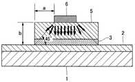
次に、コールドスプレーにより回路パターン3上に積層する上積み回路パターン5の厚みの最適化について説明する。
図2は上積み回路パターンの厚みについての説明図である。Next, optimization of the thickness of the stacked
FIG. 2 is an explanatory diagram of the thickness of the stacked circuit pattern.
パワー半導体6から発生する熱流は、通常、斜め45度の角度で拡散し広がるという性質を有している。したがって、パワー半導体6のチップ端部から上積み回路パターン5の端部までの距離aは、回路パターン3および上積み回路パターン5の合計の厚みbと等しければ、ヒートスプレッダ効果が最大に発揮され、熱抵抗を大幅に低減することができる。このため、パワー半導体6の大きさに対して無理に回路パターン3および上積み回路パターン5の幅を広げる必要はないし、無理に上積み回路パターン5の厚みを増加させる必要もない。 The heat flow generated from the
以上の上積み回路パターン5の幅および厚みの関係から、搭載されるパワー半導体6の端部から上積み回路パターン5の端部までの距離aと回路パターン3および上積み回路パターン5の合計の厚みbとの比は、1が最適であるが、0.8〜1.2の範囲であれば、実質的に十分な熱拡散性が得られる。これが0.8未満では十分な熱拡散性が得られない場合が生じ、1.2を超えても効果は飽和することになる。 From the above relationship between the width and thickness of the stacked
なお、以上の実施の形態では、絶縁層またはセラミックス絶縁板に銅などの金属箔を張り合わせ、その金属箔を加工して所定の回路パターンを形成したプリント配線板に適用した場合について詳述したが、リードフレームの回路パターンの厚み調整に適用することもできる。 In the above embodiment, the case where a metal foil such as copper is bonded to an insulating layer or a ceramic insulating plate and the metal foil is processed to form a predetermined circuit pattern is described in detail. Also, it can be applied to the adjustment of the thickness of the circuit pattern of the lead frame.
1 ベース金属
2 絶縁層
3 回路パターン
4 マスク
5 上積み回路パターン
6 パワー半導体
7 ワイヤ
101 ベース金属
102 絶縁層
103 回路パターン
104 セラミックス絶縁板
105 はんだ層
DESCRIPTION OF
Claims (2)
Translated fromJapanese発熱半導体部品が搭載される部分の前記回路パターンの上部にコールドスプレー法により金属材料を積層して上積み回路パターンを形成し、前記上積み回路パターンは、前記回路パターンを含めた合計の厚みが搭載される半導体チップの端部から前記上積み回路パターンの端部までの距離に等しくなるまで前記コールドスプレー法にて形成されることを特徴とする配線基板の製造方法。 An upper circuit pattern is formed by laminating a metal material on the upper part of the circuit pattern where the heat generating semiconductor component is mounted by a cold spray method, and the total thickness including the circuit pattern is mounted on the upper circuit pattern. A method of manufacturing a wiring board, wherein the method is formed by the cold spray method until the distance from the end of the semiconductor chip to the end of the stacked circuit pattern becomes equal to the distance.
発熱半導体部品が搭載される部分の前記回路パターンの上部にコールドスプレー法により金属材料を積層して上積み回路パターンを形成し、前記上積み回路パターンは、搭載される半導体チップの端部から前記上積み回路パターンの端部までの距離と前記回路パターンおよび前記上積み回路パターンの合計の厚みとの比が0.8〜1.2の範囲になるまで前記コールドスプレー法にて形成されることを特徴とする配線基板の製造方法。 A stacked material pattern is formed by laminating a metal material by a cold spray method on an upper portion of the circuit pattern of a portion where a heat generating semiconductor component is mounted, and the stacked circuit pattern is formed from an end portion of the mounted semiconductor chip. It is formed by the cold spray method until the ratio of the distance to the end of the pattern and the total thickness of the circuit pattern and the overlaid circuit pattern is in the range of 0.8 to 1.2. A method for manufacturing a wiring board.
Priority Applications (5)
| Application Number | Priority Date | Filing Date | Title |
|---|---|---|---|
| JP2005140498AJP4595665B2 (en) | 2005-05-13 | 2005-05-13 | Wiring board manufacturing method |
| US11/358,143US7626124B2 (en) | 2005-05-13 | 2006-02-22 | Wiring board |
| CNB2006100515605ACN100570866C (en) | 2005-05-13 | 2006-02-28 | Wiring board |
| DE102006019602.3ADE102006019602B4 (en) | 2005-05-13 | 2006-04-27 | Power semiconductor module |
| US12/585,913US8336202B2 (en) | 2005-05-13 | 2009-09-29 | Method of manufacturing a wiring board |
Applications Claiming Priority (1)
| Application Number | Priority Date | Filing Date | Title |
|---|---|---|---|
| JP2005140498AJP4595665B2 (en) | 2005-05-13 | 2005-05-13 | Wiring board manufacturing method |
Related Child Applications (1)
| Application Number | Title | Priority Date | Filing Date |
|---|---|---|---|
| JP2010168985ADivisionJP2010239164A (en) | 2010-07-28 | 2010-07-28 | Wiring board |
Publications (2)
| Publication Number | Publication Date |
|---|---|
| JP2006319146A JP2006319146A (en) | 2006-11-24 |
| JP4595665B2true JP4595665B2 (en) | 2010-12-08 |
Family
ID=37311270
Family Applications (1)
| Application Number | Title | Priority Date | Filing Date |
|---|---|---|---|
| JP2005140498AExpired - Fee RelatedJP4595665B2 (en) | 2005-05-13 | 2005-05-13 | Wiring board manufacturing method |
Country Status (4)
| Country | Link |
|---|---|
| US (2) | US7626124B2 (en) |
| JP (1) | JP4595665B2 (en) |
| CN (1) | CN100570866C (en) |
| DE (1) | DE102006019602B4 (en) |
Families Citing this family (56)
| Publication number | Priority date | Publication date | Assignee | Title |
|---|---|---|---|---|
| JP4662361B2 (en)* | 2006-01-23 | 2011-03-30 | 株式会社小糸製作所 | Light source module |
| JP2008053548A (en)* | 2006-08-25 | 2008-03-06 | Sharp Corp | Circuit board and electric circuit inspection method |
| JP5150076B2 (en)* | 2006-09-15 | 2013-02-20 | 株式会社豊田自動織機 | Surface mounting structure of electronic components for surface mounting |
| US7957158B2 (en)* | 2006-10-31 | 2011-06-07 | Sanyo Electric Co., Ltd. | Circuit device |
| DE102006061435A1 (en)* | 2006-12-23 | 2008-06-26 | Leoni Ag | Method and device for spraying in particular a conductor track, electrical component with a conductor track and metering device |
| KR100834515B1 (en)* | 2007-03-07 | 2008-06-02 | 삼성전기주식회사 | Forming method of photoresist laminated substrate using metal nanoparticle aerosol, plating method of insulating substrate, surface treatment method of metal layer of circuit board and manufacturing method of multilayer ceramic capacitor |
| JP4986657B2 (en)* | 2007-03-09 | 2012-07-25 | パナソニック株式会社 | Brushless motor |
| EP2157607A4 (en)* | 2007-05-30 | 2012-09-05 | Kyocera Corp | LAMINATED HEAT-DISPOSING BASE BODY AND HEAT DISPOSAL UNIT AND ELECTRONIC DEVICE WITH LAMINATED HEAT-DISINFECTING BASE BODY |
| DE102007050405B4 (en)* | 2007-10-22 | 2010-09-09 | Continental Automotive Gmbh | Electrical power component, in particular power semiconductor module, with a cooling device and method for surface and heat-conducting bonding of a cooling device to an electrical power component |
| US20090141456A1 (en)* | 2007-11-30 | 2009-06-04 | Itt Manufacturing Enterprises, Inc. | Multilayer, thermally-stabilized substrate structures |
| JP5321942B2 (en)* | 2008-02-29 | 2013-10-23 | 新東工業株式会社 | Method for manufacturing electronic circuit board and electronic circuit board |
| KR101013078B1 (en)* | 2008-05-09 | 2011-02-08 | (주)세렉트론 | Manufacturing method of electrode using low temperature spraying method and electrode |
| DE102009033029A1 (en)* | 2009-07-02 | 2011-01-05 | Electrovac Ag | Electronic device |
| JP5359644B2 (en)* | 2009-07-23 | 2013-12-04 | 三菱マテリアル株式会社 | Power module substrate, power module, and method of manufacturing power module substrate |
| EP2315242A1 (en)* | 2009-10-23 | 2011-04-27 | ABB Technology AG | Circuit arrangement and manufacturing method thereof |
| JP5186528B2 (en)* | 2010-04-23 | 2013-04-17 | 日本発條株式会社 | Conductive member and manufacturing method thereof |
| KR101401764B1 (en) | 2010-05-12 | 2014-05-30 | 도요타지도샤가부시키가이샤 | Semiconductor device |
| KR101343289B1 (en) | 2010-05-18 | 2013-12-18 | 도요타지도샤가부시키가이샤 | Semiconductor device and method for manufacturing the same |
| US8436461B2 (en) | 2010-05-21 | 2013-05-07 | Toyota Jidosha Kabushiki Kaisha | Semiconductor device |
| DE102010039728A1 (en)* | 2010-08-25 | 2012-03-01 | Robert Bosch Gmbh | Method for producing an electrical circuit and electrical circuit |
| US20120193126A1 (en)* | 2011-01-31 | 2012-08-02 | General Electric Company | Method of forming sensors and circuits on components |
| JP2013012531A (en)* | 2011-06-28 | 2013-01-17 | Kyocera Corp | Member for mounting electronic component and electronic apparatus |
| US9335296B2 (en) | 2012-10-10 | 2016-05-10 | Westinghouse Electric Company Llc | Systems and methods for steam generator tube analysis for detection of tube degradation |
| EP2919286A4 (en)* | 2012-11-06 | 2016-05-11 | Ngk Insulators Ltd | SUBSTRATE FOR LIGHT EMITTING DIODES |
| WO2014073039A1 (en)* | 2012-11-06 | 2014-05-15 | 日本碍子株式会社 | Substrate for light emitting diodes |
| DE102012224376A1 (en)* | 2012-12-27 | 2014-07-03 | Robert Bosch Gmbh | Printed circuit arrangement and method for its production |
| JP6037885B2 (en)* | 2013-02-19 | 2016-12-07 | 三菱重工業株式会社 | Deposition method |
| US9147631B2 (en) | 2013-04-17 | 2015-09-29 | Infineon Technologies Austria Ag | Semiconductor power device having a heat sink |
| WO2015104954A1 (en)* | 2014-01-10 | 2015-07-16 | 古河電気工業株式会社 | Electronic circuit device |
| CN103841784A (en)* | 2014-03-18 | 2014-06-04 | 亚超特工业有限公司 | Forming method of internal middle frame board of electronic device and internal middle frame board |
| DE102014217186A1 (en)* | 2014-08-28 | 2016-03-03 | Continental Automotive Gmbh | Method for producing a circuit carrier and circuit carrier for electronic components |
| CN104363697B (en)* | 2014-10-16 | 2017-12-29 | 金壬海 | The aluminium substrate copper-clad plate of ceramic filler medium and its manufacture method |
| DE102015201927A1 (en)* | 2015-02-04 | 2016-08-04 | Siemens Aktiengesellschaft | Method for cold gas spraying with mask |
| JP6400501B2 (en)* | 2015-02-18 | 2018-10-03 | Dowaメタルテック株式会社 | Metal-ceramic circuit board manufacturing method |
| JP6370257B2 (en)* | 2015-04-27 | 2018-08-08 | 三菱電機株式会社 | Semiconductor device |
| KR102424402B1 (en) | 2015-08-13 | 2022-07-25 | 삼성전자주식회사 | Semiconductor packages and methods for fabricating the same |
| JP6454262B2 (en) | 2015-12-24 | 2019-01-16 | タツタ電線株式会社 | Solder connection structure and film forming method |
| DE102016001810A1 (en)* | 2016-02-17 | 2017-08-17 | Häusermann GmbH | Method for producing a printed circuit board with reinforced copper structure |
| US9532448B1 (en)* | 2016-03-03 | 2016-12-27 | Ford Global Technologies, Llc | Power electronics modules |
| CN106158764A (en)* | 2016-08-30 | 2016-11-23 | 无锡新洁能股份有限公司 | Power model base plate and power model |
| WO2018135490A1 (en)* | 2017-01-17 | 2018-07-26 | デンカ株式会社 | Method for producing ceramic circuit board |
| CN110476244B (en) | 2017-03-31 | 2023-11-03 | 罗姆股份有限公司 | Power module and manufacturing method |
| JP7369508B2 (en)* | 2017-08-04 | 2023-10-26 | デンカ株式会社 | ceramic circuit board |
| JP7299671B2 (en)* | 2017-08-04 | 2023-06-28 | デンカ株式会社 | ceramic circuit board |
| WO2019036304A1 (en)* | 2017-08-18 | 2019-02-21 | Thin Film Electronics Asa | Spray coated sense lines, security and/or identification tags and devices including the same, and methods of manufacturing |
| WO2019103028A1 (en)* | 2017-11-22 | 2019-05-31 | 三菱電機株式会社 | Semiconductor device and method for manufacturing semiconductor device |
| US11935662B2 (en) | 2019-07-02 | 2024-03-19 | Westinghouse Electric Company Llc | Elongate SiC fuel elements |
| US11662300B2 (en) | 2019-09-19 | 2023-05-30 | Westinghouse Electric Company Llc | Apparatus for performing in-situ adhesion test of cold spray deposits and method of employing |
| DE102019215793A1 (en)* | 2019-10-14 | 2021-04-15 | Vitesco Technologies GmbH | Wiring substrate for a semiconductor device and method for manufacturing a wiring substrate |
| DE102020202607A1 (en) | 2020-02-28 | 2021-09-02 | Siemens Aktiengesellschaft | Electronic module, method for manufacturing an electronic module and industrial plant |
| KR102707682B1 (en) | 2020-03-19 | 2024-09-19 | 삼성전자주식회사 | Semiconductor module |
| DE102020109557B3 (en)* | 2020-04-06 | 2021-07-29 | Infineon Technologies Ag | METHOD OF MANUFACTURING A SEMI-CONDUCTOR ENCLOSURE, SEMICONDUCTOR ENCLOSURE AND EMBEDDED PCB MODULE |
| CN111867259A (en)* | 2020-07-30 | 2020-10-30 | 南京凯泰化学科技有限公司 | Preparation method of ceramic copper-clad plate |
| CN115004359A (en)* | 2020-08-28 | 2022-09-02 | 富士电机株式会社 | semiconductor device |
| JP7567432B2 (en)* | 2020-12-15 | 2024-10-16 | 三菱マテリアル株式会社 | Insulated circuit board and method for manufacturing the same |
| JP2024162622A (en) | 2023-05-11 | 2024-11-21 | 富士電機株式会社 | Semiconductor Device |
Family Cites Families (31)
| Publication number | Priority date | Publication date | Assignee | Title |
|---|---|---|---|---|
| JPS5933894A (en)* | 1982-08-19 | 1984-02-23 | 電気化学工業株式会社 | Method of producing hybrid integrated circuit board |
| US4811166A (en)* | 1986-07-02 | 1989-03-07 | Texas Instruments Incorporated | Heat dissipating member for mounting a semiconductor device and electrical circuit unit incorporating the member |
| JPS6351690A (en) | 1986-08-20 | 1988-03-04 | 松下電工株式会社 | Manufacture of ceramic wiring board |
| JPS63112969A (en) | 1986-10-31 | 1988-05-18 | Yoshio Murata | Ptisan and preparation thereof |
| JPH0831546B2 (en) | 1987-07-22 | 1996-03-27 | 電気化学工業株式会社 | High power circuit board and hybrid integrated circuit thereof |
| US5348683A (en) | 1990-02-06 | 1994-09-20 | Olin Corporation | Chloric acid - alkali metal chlorate mixtures and chlorine dioxide generation |
| EP0525644A1 (en)* | 1991-07-24 | 1993-02-03 | Denki Kagaku Kogyo Kabushiki Kaisha | Circuit substrate for mounting a semiconductor element |
| JP2772184B2 (en)* | 1991-11-07 | 1998-07-02 | 株式会社東芝 | Semiconductor device |
| US5393568A (en)* | 1992-02-28 | 1995-02-28 | Thomas J. Valente | Metalized coating process |
| KR100223504B1 (en)* | 1992-08-28 | 1999-10-15 | 다카노 야스아키 | Hybrid integrated circuit device |
| JPH0778901A (en) | 1993-06-18 | 1995-03-20 | Sumitomo Electric Ind Ltd | Semiconductor device |
| JPH07122696A (en) | 1993-10-27 | 1995-05-12 | Nippon Steel Corp | Semiconductor device |
| US6570099B1 (en)* | 1999-11-09 | 2003-05-27 | Matsushita Electric Industrial Co., Ltd. | Thermal conductive substrate and the method for manufacturing the same |
| DE19963264B4 (en) | 1999-12-17 | 2007-05-31 | Optotransmitter-Umweltschutz-Technologie E.V. | Carrier material for high-performance electronic components in SMD design and a high-performance electronic component produced therewith |
| JP2002012653A (en) | 2000-07-03 | 2002-01-15 | Denki Kagaku Kogyo Kk | Curable resin composition and metal-based circuit board using the same |
| JP2002033558A (en)* | 2000-07-18 | 2002-01-31 | Matsushita Electric Ind Co Ltd | Circuit board and its manufacturing method |
| JP4187062B2 (en) | 2000-08-24 | 2008-11-26 | 電気化学工業株式会社 | Metal base circuit board |
| JP4536240B2 (en) | 2000-10-10 | 2010-09-01 | 電気化学工業株式会社 | Curable resin composition and metal base circuit board using the same |
| JP2002203942A (en)* | 2000-12-28 | 2002-07-19 | Fuji Electric Co Ltd | Power semiconductor module |
| JP2003229508A (en) | 2001-11-28 | 2003-08-15 | Nitto Shinko Kk | High heat dissipation insulating substrate and module using it |
| US6808817B2 (en)* | 2002-03-15 | 2004-10-26 | Delphi Technologies, Inc. | Kinetically sprayed aluminum metal matrix composites for thermal management |
| US6627814B1 (en)* | 2002-03-22 | 2003-09-30 | David H. Stark | Hermetically sealed micro-device package with window |
| JP2003309292A (en) | 2002-04-15 | 2003-10-31 | Citizen Electronics Co Ltd | Metal core substrate for surface mounted light emitting diode and method of manufacturing the same |
| US7476422B2 (en) | 2002-05-23 | 2009-01-13 | Delphi Technologies, Inc. | Copper circuit formed by kinetic spray |
| US7244965B2 (en) | 2002-09-04 | 2007-07-17 | Cree Inc, | Power surface mount light emitting die package |
| JP4023397B2 (en) | 2003-04-15 | 2007-12-19 | 富士電機機器制御株式会社 | Semiconductor module and manufacturing method thereof |
| DE10331208A1 (en)* | 2003-07-10 | 2005-02-10 | Newspray Gmbh | Method for securing electric or electronic components, generating waste heat, to cooler of aluminum, or its alloy, with cooler enameled, at least in fastening region of components, |
| US7232957B2 (en)* | 2003-09-25 | 2007-06-19 | Sanyo Electric Co., Ltd. | Hybrid integrated circuit device and method of manufacturing the same |
| US7128948B2 (en)* | 2003-10-20 | 2006-10-31 | The Boeing Company | Sprayed preforms for forming structural members |
| US20050147742A1 (en)* | 2004-01-07 | 2005-07-07 | Tokyo Electron Limited | Processing chamber components, particularly chamber shields, and method of controlling temperature thereof |
| US20060093736A1 (en)* | 2004-10-29 | 2006-05-04 | Derek Raybould | Aluminum articles with wear-resistant coatings and methods for applying the coatings onto the articles |
- 2005
- 2005-05-13JPJP2005140498Apatent/JP4595665B2/ennot_activeExpired - Fee Related
- 2006
- 2006-02-22USUS11/358,143patent/US7626124B2/enactiveActive
- 2006-02-28CNCNB2006100515605Apatent/CN100570866C/enactiveActive
- 2006-04-27DEDE102006019602.3Apatent/DE102006019602B4/enactiveActive
- 2009
- 2009-09-29USUS12/585,913patent/US8336202B2/enactiveActive
Also Published As
| Publication number | Publication date |
|---|---|
| CN100570866C (en) | 2009-12-16 |
| US20100041228A1 (en) | 2010-02-18 |
| DE102006019602B4 (en) | 2021-01-28 |
| CN1862795A (en) | 2006-11-15 |
| JP2006319146A (en) | 2006-11-24 |
| US20060258055A1 (en) | 2006-11-16 |
| US7626124B2 (en) | 2009-12-01 |
| DE102006019602A1 (en) | 2006-11-23 |
| US8336202B2 (en) | 2012-12-25 |
Similar Documents
| Publication | Publication Date | Title |
|---|---|---|
| JP4595665B2 (en) | Wiring board manufacturing method | |
| JP5077529B2 (en) | Insulating substrate manufacturing method and semiconductor device manufacturing method | |
| JP6024750B2 (en) | Semiconductor module | |
| JP4844702B1 (en) | Masking jig, substrate heating apparatus, and film forming method | |
| CN103828040B (en) | The manufacture method of heat-radiating structure, power model, the manufacture method of heat-radiating structure and power model | |
| US7256431B2 (en) | Insulating substrate and semiconductor device having a thermally sprayed circuit pattern | |
| JP6332439B2 (en) | Power converter | |
| JP4023397B2 (en) | Semiconductor module and manufacturing method thereof | |
| WO2015064430A1 (en) | Laminate body, insulating cooling plate, power module, and production method for laminate body | |
| JP5971333B2 (en) | Power converter | |
| WO2015019890A1 (en) | Heat sink, power module, and method for manufacturing heat sink | |
| WO2013047330A1 (en) | Joint | |
| JP5644806B2 (en) | Insulating substrate, semiconductor device and manufacturing method thereof | |
| WO2016021561A1 (en) | Composite substrate and power module | |
| US9532448B1 (en) | Power electronics modules | |
| JP2006278558A (en) | Insulated heat transmission structure and substrate for use of power module | |
| JP2013168421A (en) | Wiring board and manufacturing method of the same | |
| JP2010239164A (en) | Wiring board | |
| JP4492257B2 (en) | Semiconductor module and manufacturing method thereof | |
| JP2015002306A (en) | Insulating substrate and manufacturing method therefor | |
| JP2013191722A (en) | Wiring board and manufacturing method of the same |
Legal Events
| Date | Code | Title | Description |
|---|---|---|---|
| A711 | Notification of change in applicant | Free format text:JAPANESE INTERMEDIATE CODE: A711 Effective date:20080204 | |
| RD03 | Notification of appointment of power of attorney | Free format text:JAPANESE INTERMEDIATE CODE: A7423 Effective date:20080204 | |
| RD04 | Notification of resignation of power of attorney | Free format text:JAPANESE INTERMEDIATE CODE: A7424 Effective date:20080205 | |
| A621 | Written request for application examination | Free format text:JAPANESE INTERMEDIATE CODE: A621 Effective date:20080313 | |
| A711 | Notification of change in applicant | Free format text:JAPANESE INTERMEDIATE CODE: A712 Effective date:20091112 | |
| RD03 | Notification of appointment of power of attorney | Free format text:JAPANESE INTERMEDIATE CODE: A7423 Effective date:20091112 | |
| RD04 | Notification of resignation of power of attorney | Free format text:JAPANESE INTERMEDIATE CODE: A7424 Effective date:20091112 | |
| A977 | Report on retrieval | Free format text:JAPANESE INTERMEDIATE CODE: A971007 Effective date:20100222 | |
| A131 | Notification of reasons for refusal | Free format text:JAPANESE INTERMEDIATE CODE: A131 Effective date:20100309 | |
| A521 | Request for written amendment filed | Free format text:JAPANESE INTERMEDIATE CODE: A523 Effective date:20100428 | |
| A131 | Notification of reasons for refusal | Free format text:JAPANESE INTERMEDIATE CODE: A131 Effective date:20100601 | |
| A521 | Request for written amendment filed | Free format text:JAPANESE INTERMEDIATE CODE: A523 Effective date:20100728 | |
| TRDD | Decision of grant or rejection written | ||
| A01 | Written decision to grant a patent or to grant a registration (utility model) | Free format text:JAPANESE INTERMEDIATE CODE: A01 Effective date:20100824 | |
| A01 | Written decision to grant a patent or to grant a registration (utility model) | Free format text:JAPANESE INTERMEDIATE CODE: A01 | |
| A61 | First payment of annual fees (during grant procedure) | Free format text:JAPANESE INTERMEDIATE CODE: A61 Effective date:20100906 | |
| R150 | Certificate of patent or registration of utility model | Free format text:JAPANESE INTERMEDIATE CODE: R150 Ref document number:4595665 Country of ref document:JP Free format text:JAPANESE INTERMEDIATE CODE: R150 | |
| FPAY | Renewal fee payment (event date is renewal date of database) | Free format text:PAYMENT UNTIL: 20131001 Year of fee payment:3 | |
| FPAY | Renewal fee payment (event date is renewal date of database) | Free format text:PAYMENT UNTIL: 20131001 Year of fee payment:3 | |
| S111 | Request for change of ownership or part of ownership | Free format text:JAPANESE INTERMEDIATE CODE: R313111 | |
| FPAY | Renewal fee payment (event date is renewal date of database) | Free format text:PAYMENT UNTIL: 20131001 Year of fee payment:3 | |
| R350 | Written notification of registration of transfer | Free format text:JAPANESE INTERMEDIATE CODE: R350 | |
| R250 | Receipt of annual fees | Free format text:JAPANESE INTERMEDIATE CODE: R250 | |
| R250 | Receipt of annual fees | Free format text:JAPANESE INTERMEDIATE CODE: R250 | |
| R250 | Receipt of annual fees | Free format text:JAPANESE INTERMEDIATE CODE: R250 | |
| R250 | Receipt of annual fees | Free format text:JAPANESE INTERMEDIATE CODE: R250 | |
| R250 | Receipt of annual fees | Free format text:JAPANESE INTERMEDIATE CODE: R250 | |
| R250 | Receipt of annual fees | Free format text:JAPANESE INTERMEDIATE CODE: R250 | |
| R250 | Receipt of annual fees | Free format text:JAPANESE INTERMEDIATE CODE: R250 | |
| R250 | Receipt of annual fees | Free format text:JAPANESE INTERMEDIATE CODE: R250 | |
| R250 | Receipt of annual fees | Free format text:JAPANESE INTERMEDIATE CODE: R250 | |
| R250 | Receipt of annual fees | Free format text:JAPANESE INTERMEDIATE CODE: R250 | |
| R250 | Receipt of annual fees | Free format text:JAPANESE INTERMEDIATE CODE: R250 | |
| LAPS | Cancellation because of no payment of annual fees |