JP4584024B2 - Discharge prevention circuit and electronic device provided with the discharge prevention circuit - Google Patents
Discharge prevention circuit and electronic device provided with the discharge prevention circuitDownload PDFInfo
- Publication number
- JP4584024B2 JP4584024B2JP2005144457AJP2005144457AJP4584024B2JP 4584024 B2JP4584024 B2JP 4584024B2JP 2005144457 AJP2005144457 AJP 2005144457AJP 2005144457 AJP2005144457 AJP 2005144457AJP 4584024 B2JP4584024 B2JP 4584024B2
- Authority
- JP
- Japan
- Prior art keywords
- current
- capacitor
- discharge
- prevention circuit
- power supply
- Prior art date
- Legal status (The legal status is an assumption and is not a legal conclusion. Google has not performed a legal analysis and makes no representation as to the accuracy of the status listed.)
- Expired - Lifetime
Links
Images


Classifications
- H—ELECTRICITY
- H02—GENERATION; CONVERSION OR DISTRIBUTION OF ELECTRIC POWER
- H02H—EMERGENCY PROTECTIVE CIRCUIT ARRANGEMENTS
- H02H3/00—Emergency protective circuit arrangements for automatic disconnection directly responsive to an undesired change from normal electric working condition with or without subsequent reconnection ; integrated protection
- H02H3/18—Emergency protective circuit arrangements for automatic disconnection directly responsive to an undesired change from normal electric working condition with or without subsequent reconnection ; integrated protection responsive to reversal of direct current
Landscapes
- Emergency Protection Circuit Devices (AREA)
- Protection Of Static Devices (AREA)
- Charge And Discharge Circuits For Batteries Or The Like (AREA)
- Control Of Voltage And Current In General (AREA)
- Direct Current Feeding And Distribution (AREA)
Description
Translated fromJapaneseこの発明は、放電防止回路及び該放電防止回路が設けられている電子機器に係り、特に、電源入力部にエネルギー蓄積用のコンデンサが設けられている電子機器に対して給電ラインから直流電源電圧が供給されている状態で、同様の電子機器が同給電ラインに逐次追加接続されるときに、同コンデンサの放電を防止する放電防止回路及び該放電防止回路が設けられている電子機器に関する。 The present invention relates to a discharge prevention circuit and an electronic device provided with the discharge prevention circuit, and in particular, a DC power supply voltage is applied from a power supply line to an electronic device provided with an energy storage capacitor in a power input portion. The present invention relates to a discharge prevention circuit for preventing discharge of the same capacitor and an electronic device provided with the discharge prevention circuit when the same electronic device is sequentially additionally connected to the power supply line in a supplied state.
近年、携帯電話機やインターネット接続の需要の増大に伴い、通信事業者側で通信機器の増設が増加している。各通信機器には、電源装置から給電ラインを介して直流電源が供給されている。この場合、電源装置の電源容量及び各通信機器の消費電力に基づいて、1つの電源装置に接続が可能な通信機器の数が決まる。各通信機器の電源入力部には、一般に、エネルギー蓄積用の大容量コンデンサが内蔵されていることが多いが、既設の通信機器に対して給電ラインから直流電源電圧が供給されている状態で、増設用の通信機器が同給電ラインに逐次追加接続されたとき、この増設用の通信機器の電源入力部のコンデンサが充電されるため、同給電ラインの直流電源電圧が瞬間的に低下し、既設の通信機器の動作が停止して通信サービスが停止するという問題が発生することがある。この問題に対する対策として、特許文献1に記載された放電防止回路がある。 In recent years, with the increase in demand for mobile phones and Internet connections, the number of communication devices has increased on the telecommunications carrier side. Each communication device is supplied with DC power from a power supply device via a power supply line. In this case, the number of communication devices that can be connected to one power supply device is determined based on the power supply capacity of the power supply device and the power consumption of each communication device. In general, a large-capacity capacitor for energy storage is often built in the power input unit of each communication device, but in a state where a DC power supply voltage is supplied from a power supply line to an existing communication device, When an additional communication device is sequentially connected to the same power supply line, the capacitor of the power input section of this additional communication device is charged, so the DC power supply voltage of the power supply line drops momentarily and There may be a problem that the operation of the communication device stops and the communication service stops. As a countermeasure against this problem, there is a discharge prevention circuit described in
図9は、特許文献1に記載された放電防止回路が設けられている電子機器の要部の電気的構成を示す回路図である。
この電子機器は、直流電源装置1に給電ライン2を介して接続されている通信機器10であり、コンデンサ11を電源入力部に有している。コンデンサ11は、直流電源装置1の直流電源電圧Vinが印加されて充電されると共に、通信機器10の内部回路などで構成される負荷12に電源を供給する。また、通信機器10には、放電防止回路としてダイオード13が設けられている。ダイオード13は、たとえば、給電ライン2に通信機器10と同様の機器が接続されて直流電源電圧Vinが瞬間的に低下したとき、充電されているコンデンサ11から給電ライン2への電流の逆流を防止し、同コンデンサ11の放電を防止する。FIG. 9 is a circuit diagram showing an electrical configuration of a main part of an electronic device provided with the discharge prevention circuit described in
This electronic device is a communication device 10 connected to the DC
この通信機器10では、放電防止回路は、受動素子であるダイオード13のみで構成されているため、特別な制御を必要とせず、簡単な構成となっている。しかしながら、この放電防止回路では、負荷電流をIo、ダイオード13の順電圧をVfとすると、常にIo×Vfの電力が消費される。このため、ダイオード13は、複数のダイオードを並列接続して構成し、かつ大型放熱器で放熱する必要があり、実装規模が大きい。従って、この放電防止回路は、消費電流の大きい機器に設けることは困難である。 In this communication device 10, the discharge prevention circuit is configured only by the
図10は、特許文献1に記載された他の放電防止回路が設けられている電子機器の要部の電気的構成を示す回路図であり、図9中の要素と共通の要素には共通の符号が付されている。
この電子機器は、直流電源装置1に給電ライン2を介して接続されている通信機器10Aである。この通信機器10Aでは、放電防止回路として、図9中のダイオード13に代えて、カレントトランス14と、制御回路15と、nチャネル型のMOSFET16とが設けられている。FIG. 10 is a circuit diagram showing an electrical configuration of a main part of an electronic apparatus provided with another discharge prevention circuit described in
This electronic device is a communication device 10 </ b> A that is connected to the DC
この通信機器10Aでは、定常時では、MOSFET16がオン状態となり、直流電源装置1の直流電源電圧Vinがカレントトランス14を経てコンデンサ11に印加されて充電されると共に、負荷12に電源が供給されている。そして、給電ライン2に通信機器10と同様の機器が接続されて直流電源電圧Vinが瞬間的に低下したとき、充電されているコンデンサ11から給電ライン2へ電流が逆流しようとするが、これがカレントトランス14で検出されて逆流検出信号aが出力される。逆流検出信号aは制御回路15に入力され、同制御回路15から制御信号bが出力される。制御信号bにより、MOSFET16がオフ状態となり、充電されているコンデンサ11から給電ライン2への電流の逆流が防止され、同コンデンサ11の放電が防止される。また、定常時では、MOSFET16のオン抵抗による損失があるが、上記図9のダイオードを使用した放電防止回路に比較して大幅に発熱が少ない。
しかしながら、上記従来の放電防止回路では、次のような問題点があった。
すなわち、図10の放電防止回路では、電流検出用のカレントトランス14がメインの電流ラインに挿入されているため、定常時の大電流と瞬時変動電流を考慮して設計する必要があり、同カレントトランス14が大型のものになるという問題点がある。また、カレントトランス14に定常的に直流が重畳された大電流が流れるため、同カレントトランス14で損失が発生するという問題点もある。However, the conventional discharge prevention circuit has the following problems.
That is, in the discharge prevention circuit of FIG. 10, since the
この発明は、上述の事情に鑑みてなされたもので、電流検出用のカレントトランスを小型化し、回路全体の小型化を実現すると共に損失の少ない放電防止回路を提供することを目的としている。 The present invention has been made in view of the above-described circumstances, and an object of the present invention is to provide a discharge prevention circuit that can reduce the current transformer for current detection, reduce the size of the entire circuit, and reduce loss.
また、請求項1記載の発明は、給電ラインから与えられる所定の直流電源電圧が印加されて充電されると共に負荷に電源を供給するコンデンサを有する電子機器に設けられ、前記直流電源電圧が低下したとき、充電されている前記コンデンサから前記給電ラインへの放電を防止する放電防止回路に係り、前記給電ラインから前記コンデンサに対して充電電流を流す充電電流通過手段と、前記コンデンサの放電電流を検出して放電電流検出信号を生成し、かつ該コンデンサに対する前記充電電流を検出して充電電流検出信号を生成する電流検出手段と、前記放電電流検出信号に対応した第1の制御信号を生成し、かつ前記充電電流検出信号に対応した第2の制御信号を生成する制御回路と、前記第1の制御信号に基づいて前記コンデンサと前記給電ラインとの接続状態をオフ状態とする一方、前記第2の制御信号に基づいて前記コンデンサと前記給電ラインとの接続状態をオン状態とすると共に前記充電電流通過手段を短絡するスイッチ手段とを備えてなることを特徴としている。The invention according to
また、請求項2記載の発明は、請求項1記載の放電防止回路に係り、前記コンデンサに対する充電電流を制限することにより、該コンデンサに突入電流が流れることを防止する突入電流防止回路が設けられていることを特徴としている。The invention according to claim2 relates to the discharge prevention circuit according to
また、請求項3記載の発明は、請求項2記載の放電防止回路に係り、前記突入電流防止回路は、前記コンデンサからの放電電流を通過させる放電電流通過手段と、前記コンデンサに対する前記充電電流を制限する電流制限素子とから構成されていることを特徴としている。Further, an invention according to claim3, relates to a discharge preventing circuit according to claim2, wherein the inrush current preventing circuit includes: a discharge current passing means for passing a discharge current from the capacitor, the charging current to the capacitor It is characterized by comprising a current limiting element for limiting.
また、請求項4記載の発明は、請求項2記載の放電防止回路に係り、前記突入電流防止回路は、前記コンデンサからの放電電流を通過させる放電電流通過手段と、前記コンデンサに対する前記充電電流を制限する電流制限素子と、前記コンデンサに対する前記充電電流を検出して充電電流検出信号を生成し、かつ前記コンデンサの放電電流を検出して放電電流検出信号を生成する電流検出手段と、前記充電電流検出信号に対応した第3の制御信号を生成し、かつ前記放電電流検出信号に対応した第4の制御信号を生成する制御回路と、前記第3の制御信号に基づいてオフ状態となる一方、前記第4の制御信号に基づいてオン状態となって前記電流制限素子及び放電電流通過手段を短絡する補助スイッチ手段とから構成されていることを特徴としている。According to afourth aspect of the present invention, there is provided the discharge prevention circuit according to thesecond aspect , wherein the inrush current prevention circuit includes a discharge current passage means for passing a discharge current from the capacitor, and the charging current for the capacitor. A current limiting element for limiting, a current detection means for detecting the charging current for the capacitor to generate a charging current detection signal, and detecting a discharging current of the capacitor to generate a discharging current detection signal; and the charging current A control circuit for generating a third control signal corresponding to the detection signal and generating a fourth control signal corresponding to the discharge current detection signal; and an off state based on the third control signal, And an auxiliary switch means that is turned on based on the fourth control signal to short-circuit the current limiting element and the discharge current passing means. To have.
また、請求項5記載の発明は、電子機器に係り、請求項1乃至4のいずれか一に記載の放電防止回路が設けられていることを特徴としている。
Afifth aspect of the present invention relates to an electronic apparatus, wherein the discharge prevention circuit according to any one of the first tofourth aspects is provided.
この発明の構成によれば、放電防止回路は、コンデンサの放電の開始を検出したとき、同コンデンサと給電ラインとの接続状態をオフ状態とする構成とされているので、定常時の大電流が流れることを想定する必要がなく、回路規模を小型化できる。また、制御回路により、放電電流検出信号に対応した第1の制御信号が生成され、かつ充電電流検出信号に対応した第2の制御信号が生成され、スイッチ手段により、同第1の制御信号に基づいてコンデンサと給電ラインとの接続状態がオフ状態となり、また、第2の制御信号に基づいて同コンデンサと同給電ラインとの接続状態がオン状態となると共に充電電流通過手段が短絡されるので、同スイッチ手段がオフ状態のときの損失を低減できる。 According to the configuration of the present invention, when the discharge prevention circuit detects the start of the discharge of the capacitor, the connection state between the capacitor and the power supply line is turned off. There is no need to assume the flow, and the circuit scale can be reduced. In addition, a first control signal corresponding to the discharge current detection signal is generated by the control circuit, and a second control signal corresponding to the charge current detection signal is generated, and the first control signal is generated by the switch means. Since the connection state between the capacitor and the power supply line is turned off based on the second control signal, the connection state between the capacitor and the power supply line is turned on based on the second control signal, and the charging current passing means is short-circuited. The loss when the switch means is off can be reduced.
また、突入電流防止回路が設けられているので、スイッチ手段がオフ状態のときの損失を更に低減できる。また、制御回路により、充電電流検出信号に対応した第3の制御信号が生成され、かつ放電電流検出信号に対応した第4の制御信号が生成され、補助スイッチ手段が、同第3の制御信号に基づいてオフ状態となる一方、同第4の制御信号に基づいてオン状態となって電流制限素子及び放電電流通過手段が短絡されるので、スイッチ手段がオフ状態のときでも、負荷に印加される電圧がコンデンサの電圧と同一となり、同コンデンサによるバックアップ時間が短くなることがない。このため、負荷は、低電圧仕様のものでも、正常に動作することができる。 Moreover, since the inrush current prevention circuit is provided, the loss when the switch means is in the OFF state can be further reduced. Further, the control circuit generates a third control signal corresponding to the charging current detection signal and generates a fourth control signal corresponding to the discharge current detection signal. Is turned off based on the fourth control signal, and the current limiting element and the discharge current passing means are short-circuited, so that even when the switch means is turned off, it is applied to the load. Therefore, the backup time by the capacitor is not shortened. For this reason, even if the load has a low voltage specification, it can operate normally.
コンデンサの放電電流がカレントトランスで検出されたとき、MOSFET(スイッチ手段)がオフ状態となり、同コンデンサと給電ラインとの接続状態をオフ状態とする放電防止回路を提供する。 When a discharge current of a capacitor is detected by a current transformer, a discharge prevention circuit is provided in which a MOSFET (switch means) is turned off and a connection state between the capacitor and a power supply line is turned off.
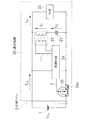
図1は、この発明の第1の実施例である放電防止回路が設けられている電子機器の要部の電気的構成を示す回路図である。
この例の電子機器は、同図に示すように、直流電源装置1に給電ライン2を介して接続されている通信機器20であり、コンデンサ21を有している。コンデンサ21は、直流電源装置1の直流電源電圧Vinが印加されて充電されると共に、通信機器20の内部回路などで構成される負荷22に電源を供給する。また、通信機器20には、放電防止回路として、カレントトランス23と、制御回路24と、nチャネル型のMOSFET25とが設けられている。FIG. 1 is a circuit diagram showing an electrical configuration of a main part of an electronic apparatus provided with a discharge prevention circuit according to a first embodiment of the present invention.
The electronic apparatus of this example is a communication apparatus 20 that is connected to the DC
カレントトランス23は、一次側にコンデンサ21の充放電電流のみが流れるように同コンデンサ21と直列接続され、同コンデンサ21の放電電流を検出して、二次側で放電電流検出信号cを生成して出力する。制御回路24は、放電電流検出信号cに基づいてMOSFET25をオフ状態とするための制御信号dを生成する。MOSFET25は、定常時では、ドレーン・ソース間がオン状態となっているが、制御信号dに基づいてコンデンサ21と給電ライン2との接続状態をオフ状態とする。また、MOSFET25は、寄生ダイオード25aを有している。 The
図2は、図1の放電防止回路の動作を説明するタイムチャートである。
この図を参照して、この例の放電防止回路の動作について説明する。
通信機器20に対して給電ライン2から直流電源電圧Vinが供給されている状態で、図示しない増設用の通信機器が同給電ライン2に逐次追加接続されたとき、この増設用の通信機器の電源入力部のコンデンサが充電されるため、直流電源電圧Vinが瞬間的に低下する。このとき、この放電防止回路では、コンデンサ21の放電電流Icにより放電の開始が検出され、同コンデンサ21と給電ライン2との接続状態がオフ状態となる。FIG. 2 is a time chart for explaining the operation of the discharge prevention circuit of FIG.
The operation of the discharge prevention circuit of this example will be described with reference to this figure.
When an additional communication device (not shown) is successively added to the power supply line 2 in a state where the DC power supply voltage Vin is supplied from the power supply line 2 to the communication device 20, the power supply of the additional communication device is supplied. Since the capacitor of the input unit is charged, the DC power supply voltage Vin drops instantaneously. At this time, in this discharge prevention circuit, the start of discharge is detected by the discharge current Ic of the
すなわち、図2に示すように、定常期間(時刻t0〜t1)では、コンデンサ21は充電されている状態であるため、充放電電流(すなわち、カレントトランス23の一次側電流)は流れない。このため、入力電流Iin=負荷電流Ioとなっている。また、MOSFET25は、制御回路24の制御により、オン(ON)状態を維持している。瞬断(瞬低)期間(時刻t1〜t2)では、直流電源電圧Vinが瞬時低下すると、コンデンサ21から負荷22に電力供給が行われる。このときの放電電流Icがカレントトランス23で検出され、同カレントトランス23の二次側に発生した放電電流検出信号cが制御回路24に伝達される。制御回路24から制御信号dが出力され、MOSFET25がオフ(OFF)状態となる。これにより、コンデンサ21に蓄えられた電力は、給電ライン2側に引き抜かれるルートがなくなるため、全て負荷22へ供給され、同コンデンサ21の電圧Vcが漸次低下する。 That is, as shown in FIG. 2, during the steady period (time t0 to t1), the
充電期間(時刻t2〜t3)では、直流電源電圧Vinの復旧により、再び給電ライン2から負荷22へ電力供給が行われると共に、放電して電圧Vcが低下しているコンデンサ21へ充電電流が流れる。このとき、MOSFET25は、制御信号dによりオフ状態を維持したままであるが、充電電流は同MOSFET25の寄生ダイオード25aを通して流れる。放電防止回路回復期間(時刻t3〜t4)では、制御信号dによりオフ状態に維持されていたMOSFET25が時刻t4でオン状態に戻る。定常期間(時刻t4〜)では、定常期間(時刻t0〜t1)と同様の状態に戻る。 In the charging period (time t2 to t3), when the DC power supply voltage Vin is restored, power is supplied again from the power supply line 2 to the
以上のように、この第1の実施例では、コンデンサ21の放電電流Icがカレントトランス23で検出されたとき、MOSFET25がオフ状態となるので、同コンデンサ21と給電ライン2との接続状態がオフ状態となる。このため、カレントトランス23は、瞬時電流のみ流れ、定常的に流れる直流重畳分を考慮する必要がなく、小型のもので良い。また、メインの電流ラインに挿入される部品がないので、全体の損失が少なくなる。 As described above, in the first embodiment, when the discharge current Ic of the
図3は、この発明の第2の実施例である放電防止回路が設けられている電子機器の要部の電気的構成を示す回路図であり、第1の実施例を示す図1中の要素と共通の要素には共通の符号が付されている。
この例の電子機器は、同図3に示すように、直流電源装置1に給電ライン2を介して接続されている通信機器20Aであり、図1中の制御回路24に代えて、新たな機能が付加された制御回路24Aが設けられている。また、カレントトランス23は、二次側で放電電流検出信号cを生成すると共に、コンデンサ21に対する充電電流を検出して、二次側で充電電流検出信号eを生成して出力する。制御回路24Aは、放電電流検出信号cに基づいてMOSFET25をオフ状態とするための制御信号dを生成する他、充電電流検出信号eに基づいてMOSFET25をオン状態とするための制御信号fを生成する。MOSFET25は、制御信号dに基づいてコンデンサ21と給電ライン2との接続状態をオフ状態とする他、制御信号fに基づいてコンデンサ21と給電ライン2との接続状態をオン状態とすると共に寄生ダイオード25aを短絡する。FIG. 3 is a circuit diagram showing the electrical configuration of the main part of the electronic apparatus provided with the discharge prevention circuit according to the second embodiment of the present invention, and the elements in FIG. 1 showing the first embodiment. Common elements are denoted by common reference numerals.
As shown in FIG. 3, the electronic device of this example is a communication device 20 </ b> A connected to the DC
図4は、図3の放電防止回路の動作を説明するタイムチャートである。
この図を参照して、この例の放電防止回路の動作について説明する。
この放電防止回路では、図4に示すように、充電期間(時刻t2〜t3)で、カレントトランス23の二次側で充電電流検出信号eが生成され、制御回路24Aで同充電電流検出信号eに基づいてMOSFET25をオン状態とするための制御信号fが生成される。このため、制御信号dによりオフ状態になっていたMOSFET25が、図2中の時刻t4よりも早い時刻t2でオン状態に戻る。これにより、MOSFET25がオフ状態のときの損失(Io×Vf、Vf;寄生ダイオード25aの順電圧)が低減される。FIG. 4 is a time chart for explaining the operation of the discharge prevention circuit of FIG.
The operation of the discharge prevention circuit of this example will be described with reference to this figure.
In this discharge prevention circuit, as shown in FIG. 4, the charging current detection signal e is generated on the secondary side of the
図5は、この発明の第3の実施例である放電防止回路が設けられている電子機器の要部の電気的構成を示す回路図であり、第2の実施例を示す図3中の要素と共通の要素には共通の符号が付されている。
この例の電子機器は、同図5に示すように、直流電源装置1に給電ライン2を介して接続されている通信機器20Bである。通信機器20Bでは、コンデンサ21にダイオード26が直列接続され、同ダイオード26に抵抗27が並列接続されている。抵抗27は、コンデンサ21に対する充電電流を制限する。ダイオード26は、コンデンサ21の放電電流に対して抵抗27をバイパスする。これらのダイオード26及び抵抗27で、突入電流防止回路が構成されている。FIG. 5 is a circuit diagram showing the electrical configuration of the main part of an electronic apparatus provided with a discharge prevention circuit according to a third embodiment of the present invention, and the elements in FIG. 3 showing the second embodiment. Common elements are denoted by common reference numerals.
The electronic device of this example is a communication device 20 </ b> B connected to the DC
図6は、図5の放電防止回路の動作を説明するタイムチャートである。
この図を参照して、この例の放電防止回路の動作について説明する。
この放電防止回路では、図6に示すように、充電期間(時刻t2〜t3)で、コンデンサ21の過大な充電電流が抑制される。これにより、MOSFET25がオフ状態のときの損失が、より低減される。但し、この実施例では、瞬断期間(時刻t1〜t2)において負荷22に印加される電圧Voは、コンデンサ21の電圧Vcに対して、ダイオード26の順電圧(約0.6V)だけ低い値となる。FIG. 6 is a time chart for explaining the operation of the discharge prevention circuit of FIG.
The operation of the discharge prevention circuit of this example will be described with reference to this figure.
In this discharge prevention circuit, as shown in FIG. 6, an excessive charging current of the
図7は、この発明の第4の実施例である放電防止回路が設けられている電子機器の要部の電気的構成を示す回路図である。
この例の電子機器は、同図7に示すように、直流電源装置1に給電ライン2を介して接続されている通信機器20Cである。通信機器20Cでは、図5中のカレントトランス23、制御回路24A及びダイオード26に代えて、カレントトランス23A、制御回路24B及びMOSFET28が設けられている。カレントトランス23Aは、カレントトランス23の機能に加え、コンデンサ21に対する充電電流を検出して充電電流検出信号gを生成し、かつ同コンデンサ21の放電電流を検出して放電電流検出信号hを生成する。制御回路24Bは、制御回路24Aの機能に加え、充電電流検出信号gに対応した制御信号jを生成し、かつ放電電流検出信号hに対応した制御信号kを生成する。MOSFET28は、寄生ダイオード28aを有している。寄生ダイオード28aは、コンデンサ21からの放電電流を通過させる放電電流通過手段としての働きをする。また、MOSFET28は、制御信号jに基づいてオフ状態となり、また、制御信号kに基づいてオン状態となって抵抗27及び寄生ダイオード28aを短絡する。FIG. 7 is a circuit diagram showing the electrical configuration of the main part of an electronic apparatus provided with a discharge prevention circuit according to the fourth embodiment of the present invention.
The electronic device in this example is a communication device 20 </ b> C connected to the DC
図8は、図7の放電防止回路の動作を説明するタイムチャートである。
この図を参照して、この例の放電防止回路の動作について説明する。
この放電防止回路では、図8に示すように、瞬断期間(時刻t1〜t2)においてMOSFET28がオン状態となっているので、負荷22に印加される電圧Voがコンデンサ21の電圧Vcと同一となる。このため、コンデンサ21によるバックアップ時間が短くなることがない。また、時刻t2において、カレントトランス23Aにより、コンデンサ21に対する充電電流が検出されて充電電流検出信号gが生成され、制御回路24Bにより、同充電電流検出信号gに対応した制御信号jが生成されてMOSFET28がオフ状態となる。この後、時刻t4aにおいて、コンデンサ21の充電完了が検出されてMOSFET28がオン状態となる。また、時刻t4b〜t4cにおいて、直流電源電圧Vinが瞬時低下すると、MOSFET28がオン状態となる。このとき、MOSFET25がオフ状態となる。FIG. 8 is a time chart for explaining the operation of the discharge prevention circuit of FIG.
The operation of the discharge prevention circuit of this example will be described with reference to this figure.
In this discharge prevention circuit, as shown in FIG. 8, since the
以上のように、この第4の実施例では、瞬断期間(時刻t1〜t2)において負荷22に印加される電圧Voがコンデンサ21の電圧Vcと同一となり、同コンデンサ21によるバックアップ時間が短くなることがない。このため、負荷22が低電圧仕様(電源電圧が、たとえば3.3V±10%、すなわち、許容範囲2.97V〜3.63V)のものであっても、電圧Voが許容範囲の下限値よりも低下することがなく、正常に動作する。 As described above, in the fourth embodiment, the voltage Vo applied to the
以上、この発明の実施例を図面により詳述してきたが、具体的な構成は同実施例に限られるものではなく、この発明の要旨を逸脱しない範囲の設計の変更などがあっても、この発明に含まれる。
たとえば、MOSFET25,28は、バイポーラトランジスタ及びダイオードを組み合わせたものでも、上記実施例とほぼ同様の作用、効果が得られる。また、図7中のカレントトランス23Aは、2つのカレントトランスで構成しても良い。また、上記各実施例では、直流電源装置1のマイナス側にMOSFET25が接続されているが、同直流電源装置1のプラス側にpチャネル型のMOSFETを接続した構成にしても、上記実施例とほぼ同様の作用、効果が得られる。また、寄生ダイオード25a,28aに対して、より順電圧の小さいショットキ・バリア・ダイオードを並列接続しても良い。これにより、MOSFET25,28のオフ状態からオン状態に遷移する時間遅れが改善される。The embodiment of the present invention has been described in detail with reference to the drawings. However, the specific configuration is not limited to the embodiment, and even if there is a design change without departing from the gist of the present invention, Included in the invention.
For example, even if the
この発明は、電源入力部にエネルギー蓄積用のコンデンサが設けられている電子機器に対して給電ラインから直流電源電圧が供給されている状態で、同様の電子機器が同給電ラインに逐次追加接続される場合全般に適用でき、特に、同コンデンサの放電防止回路を小形化する場合に有効である。 In the present invention, in a state where a DC power supply voltage is supplied from a power supply line to an electronic device in which an energy storage capacitor is provided in a power input unit, similar electronic devices are sequentially added to the power supply line. In particular, it is effective when the discharge prevention circuit of the capacitor is miniaturized.
1 直流電源装置
2 給電ライン
20,20A,20B 通信機器(電子機器)
21 コンデンサ
22 負荷
23,23A カレントトランス(電流検出手段)
24,24A,24B 制御回路
25 MOSFET(スイッチ手段)
25a 寄生ダイオード(充電電流通過手段)
26 ダイオード(突入電流防止回路の一部、放電電流通過手段)
27 抵抗(突入電流防止回路の一部、電流制限素子)
28 MOSFET(突入電流防止回路の一部、補助スイッチ手段)
28a ダイオード(突入電流防止回路の一部、放電電流通過手段)1 DC power supply device 2
21
24, 24A,
25a Parasitic diode (charge current passing means)
26 Diode (part of inrush current prevention circuit, discharge current passing means)
27 Resistance (part of inrush current prevention circuit, current limiting element)
28 MOSFET (part of inrush current prevention circuit, auxiliary switch means)
28a Diode (part of inrush current prevention circuit, discharge current passing means)
Claims (5)
Translated fromJapanese前記給電ラインから前記コンデンサに対して充電電流を流す充電電流通過手段と、
前記コンデンサの放電電流を検出して放電電流検出信号を生成し、かつ該コンデンサに対する前記充電電流を検出して充電電流検出信号を生成する電流検出手段と、
前記放電電流検出信号に対応した第1の制御信号を生成し、かつ前記充電電流検出信号に対応した第2の制御信号を生成する制御回路と、
前記第1の制御信号に基づいて前記コンデンサと前記給電ラインとの接続状態をオフ状態とする一方、前記第2の制御信号に基づいて前記コンデンサと前記給電ラインとの接続状態をオン状態とすると共に前記充電電流通過手段を短絡するスイッチ手段とを備えてなることを特徴とする放電防止回路。A predetermined DC power supply voltage applied from a power supply line is applied and charged, and is provided in an electronic device having a capacitor that supplies power to a load.When the DC power supply voltage decreases, the capacitor is charged and A discharge prevention circuit for preventing discharge to the power supply line,
Charging current passing means for flowing a charging current from the power supply line to the capacitor;
Current detection means for detecting a discharge current of the capacitor to generate a discharge current detection signal, and detecting the charge current for the capacitor to generate a charge current detection signal;
A control circuit for generating a first control signal corresponding to the discharge current detection signal and generating a second control signal corresponding to the charging current detection signal;
The connection state between the capacitor and the feed line is turned off based on the first control signal, while the connection state between the capacitor and the feed line is turned on based on the second control signal. And a switch means for short-circuiting the charging current passage means.
前記コンデンサからの放電電流を通過させる放電電流通過手段と、
前記コンデンサに対する前記充電電流を制限する電流制限素子とから構成されていることを特徴とする請求項2記載の放電防止回路。The inrush current prevention circuit is
A discharge current passing means for passing a discharge current from the capacitor;
3. The discharge prevention circuit according to claim2, further comprising a current limiting element that limits the charging current to the capacitor.
前記コンデンサからの放電電流を通過させる放電電流通過手段と、
前記コンデンサに対する前記充電電流を制限する電流制限素子と、
前記コンデンサに対する前記充電電流を検出して充電電流検出信号を生成し、かつ前記コンデンサの放電電流を検出して放電電流検出信号を生成する電流検出手段と、
前記充電電流検出信号に対応した第3の制御信号を生成し、かつ前記放電電流検出信号に対応した第4の制御信号を生成する制御回路と、
前記第3の制御信号に基づいてオフ状態となる一方、前記第4の制御信号に基づいてオン状態となって前記電流制限素子及び放電電流通過手段を短絡する補助スイッチ手段とから構成されていることを特徴とする請求項2記載の放電防止回路。The inrush current prevention circuit is
A discharge current passing means for passing a discharge current from the capacitor;
A current limiting element for limiting the charging current to the capacitor;
Current detection means for detecting the charging current for the capacitor to generate a charging current detection signal, and detecting a discharge current of the capacitor to generate a discharge current detection signal;
A control circuit for generating a third control signal corresponding to the charge current detection signal and generating a fourth control signal corresponding to the discharge current detection signal;
The auxiliary switch means is turned off based on the third control signal and turned on based on the fourth control signal to short-circuit the current limiting element and the discharge current passing means. The discharge prevention circuit according to claim2 .
Priority Applications (2)
| Application Number | Priority Date | Filing Date | Title |
|---|---|---|---|
| JP2005144457AJP4584024B2 (en) | 2005-05-17 | 2005-05-17 | Discharge prevention circuit and electronic device provided with the discharge prevention circuit |
| US11/433,580US7579707B2 (en) | 2005-05-17 | 2006-05-15 | Discharge prevention circuit and electronic equipment provided with the discharge prevention circuit |
Applications Claiming Priority (1)
| Application Number | Priority Date | Filing Date | Title |
|---|---|---|---|
| JP2005144457AJP4584024B2 (en) | 2005-05-17 | 2005-05-17 | Discharge prevention circuit and electronic device provided with the discharge prevention circuit |
Publications (2)
| Publication Number | Publication Date |
|---|---|
| JP2006325302A JP2006325302A (en) | 2006-11-30 |
| JP4584024B2true JP4584024B2 (en) | 2010-11-17 |
Family
ID=37447732
Family Applications (1)
| Application Number | Title | Priority Date | Filing Date |
|---|---|---|---|
| JP2005144457AExpired - LifetimeJP4584024B2 (en) | 2005-05-17 | 2005-05-17 | Discharge prevention circuit and electronic device provided with the discharge prevention circuit |
Country Status (2)
| Country | Link |
|---|---|
| US (1) | US7579707B2 (en) |
| JP (1) | JP4584024B2 (en) |
Families Citing this family (62)
| Publication number | Priority date | Publication date | Assignee | Title |
|---|---|---|---|---|
| US10693415B2 (en) | 2007-12-05 | 2020-06-23 | Solaredge Technologies Ltd. | Testing of a photovoltaic panel |
| US11881814B2 (en) | 2005-12-05 | 2024-01-23 | Solaredge Technologies Ltd. | Testing of a photovoltaic panel |
| US9088178B2 (en) | 2006-12-06 | 2015-07-21 | Solaredge Technologies Ltd | Distributed power harvesting systems using DC power sources |
| US8618692B2 (en) | 2007-12-04 | 2013-12-31 | Solaredge Technologies Ltd. | Distributed power system using direct current power sources |
| US11687112B2 (en) | 2006-12-06 | 2023-06-27 | Solaredge Technologies Ltd. | Distributed power harvesting systems using DC power sources |
| US8473250B2 (en) | 2006-12-06 | 2013-06-25 | Solaredge, Ltd. | Monitoring of distributed power harvesting systems using DC power sources |
| US8319483B2 (en) | 2007-08-06 | 2012-11-27 | Solaredge Technologies Ltd. | Digital average input current control in power converter |
| US11296650B2 (en) | 2006-12-06 | 2022-04-05 | Solaredge Technologies Ltd. | System and method for protection during inverter shutdown in distributed power installations |
| US11888387B2 (en) | 2006-12-06 | 2024-01-30 | Solaredge Technologies Ltd. | Safety mechanisms, wake up and shutdown methods in distributed power installations |
| US11735910B2 (en) | 2006-12-06 | 2023-08-22 | Solaredge Technologies Ltd. | Distributed power system using direct current power sources |
| US8816535B2 (en) | 2007-10-10 | 2014-08-26 | Solaredge Technologies, Ltd. | System and method for protection during inverter shutdown in distributed power installations |
| US8013472B2 (en) | 2006-12-06 | 2011-09-06 | Solaredge, Ltd. | Method for distributed power harvesting using DC power sources |
| US11855231B2 (en) | 2006-12-06 | 2023-12-26 | Solaredge Technologies Ltd. | Distributed power harvesting systems using DC power sources |
| US11569659B2 (en) | 2006-12-06 | 2023-01-31 | Solaredge Technologies Ltd. | Distributed power harvesting systems using DC power sources |
| US8319471B2 (en) | 2006-12-06 | 2012-11-27 | Solaredge, Ltd. | Battery power delivery module |
| US9112379B2 (en) | 2006-12-06 | 2015-08-18 | Solaredge Technologies Ltd. | Pairing of components in a direct current distributed power generation system |
| US9130401B2 (en) | 2006-12-06 | 2015-09-08 | Solaredge Technologies Ltd. | Distributed power harvesting systems using DC power sources |
| US8947194B2 (en) | 2009-05-26 | 2015-02-03 | Solaredge Technologies Ltd. | Theft detection and prevention in a power generation system |
| US11309832B2 (en) | 2006-12-06 | 2022-04-19 | Solaredge Technologies Ltd. | Distributed power harvesting systems using DC power sources |
| US8963369B2 (en) | 2007-12-04 | 2015-02-24 | Solaredge Technologies Ltd. | Distributed power harvesting systems using DC power sources |
| US8384243B2 (en) | 2007-12-04 | 2013-02-26 | Solaredge Technologies Ltd. | Distributed power harvesting systems using DC power sources |
| US12316274B2 (en) | 2006-12-06 | 2025-05-27 | Solaredge Technologies Ltd. | Pairing of components in a direct current distributed power generation system |
| WO2009072076A2 (en) | 2007-12-05 | 2009-06-11 | Solaredge Technologies Ltd. | Current sensing on a mosfet |
| US9291696B2 (en) | 2007-12-05 | 2016-03-22 | Solaredge Technologies Ltd. | Photovoltaic system power tracking method |
| CN105244905B (en) | 2007-12-05 | 2019-05-21 | 太阳能安吉有限公司 | Release mechanism in distributed power device is waken up and method for closing |
| WO2009073867A1 (en) | 2007-12-05 | 2009-06-11 | Solaredge, Ltd. | Parallel connected inverters |
| US11264947B2 (en) | 2007-12-05 | 2022-03-01 | Solaredge Technologies Ltd. | Testing of a photovoltaic panel |
| US8111052B2 (en) | 2008-03-24 | 2012-02-07 | Solaredge Technologies Ltd. | Zero voltage switching |
| EP2294669B8 (en) | 2008-05-05 | 2016-12-07 | Solaredge Technologies Ltd. | Direct current power combiner |
| EP2275964B1 (en)* | 2009-06-30 | 2015-03-25 | Legic Identsystems AG | Electronic circuit with capacitor |
| US9324885B2 (en) | 2009-10-02 | 2016-04-26 | Tigo Energy, Inc. | Systems and methods to provide enhanced diode bypass paths |
| US12418177B2 (en) | 2009-10-24 | 2025-09-16 | Solaredge Technologies Ltd. | Distributed power system using direct current power sources |
| US9425783B2 (en) | 2010-03-15 | 2016-08-23 | Tigo Energy, Inc. | Systems and methods to provide enhanced diode bypass paths |
| US10230310B2 (en) | 2016-04-05 | 2019-03-12 | Solaredge Technologies Ltd | Safety switch for photovoltaic systems |
| US10673222B2 (en) | 2010-11-09 | 2020-06-02 | Solaredge Technologies Ltd. | Arc detection and prevention in a power generation system |
| GB2485527B (en) | 2010-11-09 | 2012-12-19 | Solaredge Technologies Ltd | Arc detection and prevention in a power generation system |
| US10673229B2 (en) | 2010-11-09 | 2020-06-02 | Solaredge Technologies Ltd. | Arc detection and prevention in a power generation system |
| GB2486408A (en) | 2010-12-09 | 2012-06-20 | Solaredge Technologies Ltd | Disconnection of a string carrying direct current |
| GB2483317B (en) | 2011-01-12 | 2012-08-22 | Solaredge Technologies Ltd | Serially connected inverters |
| US8570005B2 (en) | 2011-09-12 | 2013-10-29 | Solaredge Technologies Ltd. | Direct current link circuit |
| GB2498365A (en) | 2012-01-11 | 2013-07-17 | Solaredge Technologies Ltd | Photovoltaic module |
| US9853565B2 (en) | 2012-01-30 | 2017-12-26 | Solaredge Technologies Ltd. | Maximized power in a photovoltaic distributed power system |
| GB2498791A (en) | 2012-01-30 | 2013-07-31 | Solaredge Technologies Ltd | Photovoltaic panel circuitry |
| GB2498790A (en) | 2012-01-30 | 2013-07-31 | Solaredge Technologies Ltd | Maximising power in a photovoltaic distributed power system |
| DE102012203072A1 (en)* | 2012-02-29 | 2013-08-29 | Zf Friedrichshafen Ag | Device and method for securing a circuit for a vehicle and circuit |
| EP2634882B1 (en)* | 2012-02-29 | 2014-09-17 | ABB Technology Ltd | DC supply unit for a power provision unit |
| GB2499991A (en) | 2012-03-05 | 2013-09-11 | Solaredge Technologies Ltd | DC link circuit for photovoltaic array |
| US10115841B2 (en) | 2012-06-04 | 2018-10-30 | Solaredge Technologies Ltd. | Integrated photovoltaic panel circuitry |
| CN104685757B (en)* | 2012-10-18 | 2018-05-22 | 瑞典爱立信有限公司 | Apparatus and method for power disturbance detection |
| US9548619B2 (en) | 2013-03-14 | 2017-01-17 | Solaredge Technologies Ltd. | Method and apparatus for storing and depleting energy |
| US9941813B2 (en) | 2013-03-14 | 2018-04-10 | Solaredge Technologies Ltd. | High frequency multi-level inverter |
| EP3506370B1 (en) | 2013-03-15 | 2023-12-20 | Solaredge Technologies Ltd. | Bypass mechanism |
| DE102013212233A1 (en) | 2013-06-26 | 2014-12-31 | Zf Friedrichshafen Ag | Device for the mechanical and electrical connection of cable cores of a cable with cable connections of an electrical assembly |
| JP6149647B2 (en)* | 2013-09-25 | 2017-06-21 | 沖電気工業株式会社 | Inrush current suppression circuit and power supply device |
| US9318974B2 (en) | 2014-03-26 | 2016-04-19 | Solaredge Technologies Ltd. | Multi-level inverter with flying capacitor topology |
| DE102014221526A1 (en)* | 2014-10-23 | 2016-05-12 | Robert Bosch Gmbh | Device for cell voltage-sensitive overcurrent interruption |
| WO2016157443A1 (en)* | 2015-03-31 | 2016-10-06 | 三菱電機株式会社 | Refrigeration cycle device |
| US12057807B2 (en) | 2016-04-05 | 2024-08-06 | Solaredge Technologies Ltd. | Chain of power devices |
| US11177663B2 (en) | 2016-04-05 | 2021-11-16 | Solaredge Technologies Ltd. | Chain of power devices |
| US11018623B2 (en) | 2016-04-05 | 2021-05-25 | Solaredge Technologies Ltd. | Safety switch for photovoltaic systems |
| IT201600125462A1 (en)* | 2016-12-13 | 2018-06-13 | Spal Automotive Srl | PROTECTION SYSTEM |
| CN117154658B (en)* | 2023-09-07 | 2024-02-06 | 上海类比半导体技术有限公司 | Protection circuit, protection chip, chip to be tested and application system |
Family Cites Families (5)
| Publication number | Priority date | Publication date | Assignee | Title |
|---|---|---|---|---|
| JPS604654B2 (en)* | 1977-04-07 | 1985-02-05 | 株式会社東芝 | Short-circuit protection device for power converter equipment with DC circuit |
| JPH07261860A (en)* | 1994-03-23 | 1995-10-13 | Sony Corp | Power circuit |
| JP2000324718A (en)* | 1999-05-14 | 2000-11-24 | Kenwood Corp | Power circuit |
| JP2002315201A (en)* | 2001-04-12 | 2002-10-25 | Nec Miyagi Ltd | Discharge prevention circuit |
| JP4053501B2 (en)* | 2004-01-13 | 2008-02-27 | ファナック株式会社 | Motor drive device |
- 2005
- 2005-05-17JPJP2005144457Apatent/JP4584024B2/ennot_activeExpired - Lifetime
- 2006
- 2006-05-15USUS11/433,580patent/US7579707B2/enactiveActive
Also Published As
| Publication number | Publication date |
|---|---|
| JP2006325302A (en) | 2006-11-30 |
| US7579707B2 (en) | 2009-08-25 |
| US20060261751A1 (en) | 2006-11-23 |
Similar Documents
| Publication | Publication Date | Title |
|---|---|---|
| JP4584024B2 (en) | Discharge prevention circuit and electronic device provided with the discharge prevention circuit | |
| KR100994452B1 (en) | Synchronous Rectified Switching Regulator | |
| US8508963B2 (en) | Step-down switching regulator capable of providing high-speed response with compact structure | |
| EP1239573B1 (en) | Overvoltage-protective device for power system, AC/DC converter and DC/DC converter constituting the power system | |
| EP2141746B1 (en) | By-pass diode structure for strings of series connected cells of a photovoltaic panel | |
| US8723364B2 (en) | Uninterruptible power supply having integrated charge/discharge circuit | |
| JP4997405B2 (en) | Power allocation device | |
| CN101047318B (en) | Power control circuit and power control method | |
| JP6203020B2 (en) | Battery pack having charge / discharge switch circuit | |
| JP5228886B2 (en) | Snubber circuit | |
| JP2012178535A (en) | Photovoltaic power generation system, switching system and bypass device | |
| US8726046B2 (en) | Integrated circuit device and control method for electrostatic protection circuit thereof | |
| JP2008154419A (en) | Switching regulator and semiconductor device constituting the switching regulator | |
| US20110260704A1 (en) | Provision of an output voltage from a wide range variable and low input voltage | |
| US20130119957A1 (en) | Bi-directional Switching Regulator and Control Circuit Thereof | |
| JP4777737B2 (en) | Electronic device having step-up DC-DC converter | |
| KR101918302B1 (en) | Semiconductor device including charging system | |
| JP5015035B2 (en) | Step-down switching regulator | |
| JP5589143B2 (en) | Auxiliary power supply unit control circuit and power supply unit device | |
| US9077256B2 (en) | Method of forming a low power dissipation regulator and structure therefor | |
| JP6288202B2 (en) | Improved DC-DC transformer for obtaining constant output voltage | |
| JP5982632B2 (en) | In-vehicle power supply circuit and in-vehicle power supply unit using the same | |
| JP2012239292A (en) | Snubber circuit of rectifier | |
| JP7146625B2 (en) | switching power supply | |
| JP2006020414A (en) | Power supply device |
Legal Events
| Date | Code | Title | Description |
|---|---|---|---|
| A621 | Written request for application examination | Free format text:JAPANESE INTERMEDIATE CODE: A621 Effective date:20080111 | |
| A977 | Report on retrieval | Free format text:JAPANESE INTERMEDIATE CODE: A971007 Effective date:20090219 | |
| A131 | Notification of reasons for refusal | Free format text:JAPANESE INTERMEDIATE CODE: A131 Effective date:20090324 | |
| A521 | Request for written amendment filed | Free format text:JAPANESE INTERMEDIATE CODE: A523 Effective date:20090525 | |
| A131 | Notification of reasons for refusal | Free format text:JAPANESE INTERMEDIATE CODE: A131 Effective date:20100525 | |
| A521 | Request for written amendment filed | Free format text:JAPANESE INTERMEDIATE CODE: A523 Effective date:20100726 | |
| TRDD | Decision of grant or rejection written | ||
| A01 | Written decision to grant a patent or to grant a registration (utility model) | Free format text:JAPANESE INTERMEDIATE CODE: A01 Effective date:20100817 | |
| A01 | Written decision to grant a patent or to grant a registration (utility model) | Free format text:JAPANESE INTERMEDIATE CODE: A01 | |
| A61 | First payment of annual fees (during grant procedure) | Free format text:JAPANESE INTERMEDIATE CODE: A61 Effective date:20100901 | |
| R150 | Certificate of patent or registration of utility model | Ref document number:4584024 Country of ref document:JP Free format text:JAPANESE INTERMEDIATE CODE: R150 Free format text:JAPANESE INTERMEDIATE CODE: R150 | |
| FPAY | Renewal fee payment (event date is renewal date of database) | Free format text:PAYMENT UNTIL: 20130910 Year of fee payment:3 | |
| EXPY | Cancellation because of completion of term |