JP4581864B2 - Method for forming through wiring on semiconductor substrate - Google Patents
Method for forming through wiring on semiconductor substrateDownload PDFInfo
- Publication number
- JP4581864B2 JP4581864B2JP2005181074AJP2005181074AJP4581864B2JP 4581864 B2JP4581864 B2JP 4581864B2JP 2005181074 AJP2005181074 AJP 2005181074AJP 2005181074 AJP2005181074 AJP 2005181074AJP 4581864 B2JP4581864 B2JP 4581864B2
- Authority
- JP
- Japan
- Prior art keywords
- semiconductor substrate
- hole
- metal
- insulating layer
- wiring
- Prior art date
- Legal status (The legal status is an assumption and is not a legal conclusion. Google has not performed a legal analysis and makes no representation as to the accuracy of the status listed.)
- Expired - Fee Related
Links
Images


Landscapes
- Electrodes Of Semiconductors (AREA)
- Internal Circuitry In Semiconductor Integrated Circuit Devices (AREA)
Description
Translated fromJapanese本発明は、半導体基板への貫通配線の形成方法に関し、例えば、ウェハレベルパッケージングなどで用いられる貫通配線の形成方法に関するものである。 The present invention relates to a method for forming a through wiring on a semiconductor substrate, for example, a method for forming a through wiring used in wafer level packaging or the like.
従来から、半導体基板への貫通配線の形成方法が各所で研究開発されている(例えば、特許文献1参照)。 Conventionally, a method for forming a through wiring on a semiconductor substrate has been researched and developed in various places (for example, see Patent Document 1).
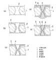
以下、上述の半導体基板への貫通配線の形成方法について図3に基づいて説明するが、図3(a)〜(c)における半導体基板1はダイシング工程により個々のチップに分離する前のウェハである。 Hereinafter, a method for forming the through wiring on the semiconductor substrate will be described with reference to FIG. 3. The
まず、半導体基板1の一表面(図3(a)の上面)における貫通孔形成予定部位にエッチング加工などによって貫通孔用の有底孔(凹部)1aを形成してから、CVD法や熱酸化法などによって半導体基板1の上記一表面および有底孔1aの内面に絶縁層3aを形成するとともに半導体基板1の他表面(図3(a)の下面)に絶縁層3bを形成することにより、図3(a)に示す構造を得る。 First, a bottomed hole (recessed portion) 1a for a through hole is formed by etching or the like at a through hole formation scheduled portion on one surface of the semiconductor substrate 1 (upper surface in FIG. 3A), and then CVD or thermal oxidation is performed. By forming the
その後、半導体基板1の上記一表面および有底孔1aの内面に形成されている絶縁層3aに金属材料(例えば、銅、ニッケルなど)からなる金属層(金属薄膜)4をCVD法やスパッタ法などによって積層してから、当該金属層4をシード層として電解メッキ法などによって金属材料(例えば、銅、ニッケルなど)からなる金属部5を析出(堆積)させることにより、図3(b)に示す構造を得る。 Thereafter, a metal layer (metal thin film) 4 made of a metal material (for example, copper, nickel, etc.) is applied to the insulating
次に、半導体基板1の上記他表面側を化学的機械的研磨(Chemical Mechanical Polishing:CMP)技術などによって研磨して金属層4を露出させるとともに貫通孔2’を完成させ、続いて、金属部5および金属層4のうち半導体基板1の上記一表面側における不要部分を除去することによって、図3(c)に示す構造を得る。ここに、図3(c)では、金属部5のうち貫通孔2’に埋め込まれている部分と金属層4のうち貫通孔2’に埋め込まれている部分とで貫通配線6を構成している。 Next, the other surface side of the
ところで、上述の電解メッキ法により金属部5を析出させる工程においては、図4(a)に示すように半導体基板1の上記一表面および有底孔1aの内面の全体に亘って形成されている絶縁層3aに積層された金属薄膜4をシード層として利用しているので、金属部5は図4(b)に示すように均一に成長するコンフォーマル成長により析出することとなる。 By the way, in the process of depositing the
しかしながら、上述のコンフォーマル成長により金属部5を析出させる方法では、有底孔1aのアスペクト比が高くなるにつれて有底孔1aの内側にボイド(空洞)が形成されてしまう(言い換えれば、有底孔1aの内側を隙間なく埋め込むことができない)という問題が起こりやすかった。また、上述のコンフォーマル成長により金属部5を析出させる方法では、有底孔1aが半導体基板1の上記一表面側において上記一表面に近づくにつれて開口面積が徐々に小さくなる形状に形成されている場合に、金属部5の成長途中で有底孔1aの内側が完全に埋め込まれないうちに半導体基板1の一表面側において有底孔1aの開口面が金属部5によって塞がれてしまって有底孔1aの内側にボイドが形成されてしまうという問題があった。 However, in the method of depositing the
そこで、ボイドの発生が起こりにくい貫通配線の形成方法として、半導体基板の厚み方向に沿って金属部が成長するボトムアップ成長により金属部を析出させる方法が提案されている。 In view of this, as a method of forming a through wiring that is less likely to generate voids, a method of depositing a metal part by bottom-up growth in which the metal part grows along the thickness direction of the semiconductor substrate has been proposed.
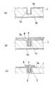
以下、ボトムアップ成長により金属部を析出させる方法を採用した貫通配線の形成方法の一例について図5に基づいて説明する。 Hereinafter, an example of a method of forming a through wiring employing a method of depositing a metal part by bottom-up growth will be described with reference to FIG.
まず、図5(a)の上側に示すようにエッチング加工などによって貫通孔2を形成した半導体基板1と、図5(a)の下側に示すように金属材料などからなる導電層14が一表面上に形成された基板15とを用意し、半導体基板1と基板15とを導電層14を介在させた形で接合あるいは貼り合わせることにより、図5(b)に示す構造を得る。 First, a
その後、導電層14をシード層として電解メッキ法により金属部5を析出させることにより、図5(c)に示す構造を得る。ここにおいて、金属部5は導電層14の表面から半導体基板1の厚み方向に沿って成長するボトムアップ成長により形成されることとなるので、貫通孔2の内側にボイドが発生しにくくなる。 Thereafter, the
さらにその後、上述の導電層14が一表面側に形成されている基板15を半導体基板1から剥離することにより、図5(d)に示す構造を得る。ここにおいて、金属部5のうち貫通孔2の内側に形成されている部分が貫通配線となる。その後は、例えば、半導体基板1の裏面(図5(d)における下面)に電極層用の導体層を形成し、当該導体層の不要部分を除去すればよい。 Thereafter, the
次に、ボトムアップ成長により金属部を析出させる方法を採用した貫通配線の形成方法の他の例について図6に基づいて説明する。 Next, another example of a method for forming a through wiring employing a method of depositing a metal part by bottom-up growth will be described with reference to FIG.
まず、半導体基板1にエッチング加工などによって厚み方向に貫通する貫通孔2を形成することにより、図6(a)に示す構造を得る。その後、CVD法や熱酸化法などによって半導体基板1の一表面(図6(a)における下面)および他表面(図6(a)における上面)および貫通孔2の内周面に絶縁層3を形成することにより、図6(b)に示す構造を得る。 First, the structure shown in FIG. 6A is obtained by forming the through
続いて、半導体基板1の上記一表面側に金属材料(例えば、銅、ニッケルなど)からなる金属層4をスパッタ法などによって形成することにより、図6(c)に示す構造を得る。続いて、金属層4をシード層として電解メッキ法によって、貫通孔2の内側が埋め込まれるように金属部5を析出させることにより、図6(e)に示す構造を得る。ここにおいて、金属部5は、図6(d)に示すように半導体基板1の上記一表面側に析出して半導体基板1の上記一表面側において貫通孔2の開口面を塞ぐように成長した部分5aと、引き続いて、ボトムアップ成長により半導体基板1の厚み方向に沿って成長した部分5b(図6(e)参照)とで構成されている。金属部5を形成した後、不要部分の除去や平坦化を目的としたCMPを行うことによって、金属部5のうち貫通孔2の内側に形成されている部分からなる貫通配線が完成する。その後は、例えば、半導体基板1の上記一表面側に電極層用の導体層を形成し、当該導体層の不要部分を除去すればよい。
ところで、上述の図5や図6のようにボトムアップ成長により金属部を析出させる方法を採用した貫通配線の形成方法では、コンフォーマル成長による埋め込みが困難な貫通孔(高アスペクト比の微細孔)への埋め込み性が改善される。しかしながら、ボトムアップ成長により形成された貫通配線では、コンフォーマル成長により成長された金属部5と当該金属部5の析出時のシード層たる金属層4とで構成される貫通配線6に比較して、貫通配線の下地である絶縁層3との密着性が低いので、金属部5の不要部分の除去や平坦化を目的としたCMPを行った場合に、金属部5のうち貫通孔2の内側に形成されている部分の一部が剥離してチップ歩留まりが低下してしまう可能性があった。また、ボトムアップ成長により形成された貫通配線では、絶縁層3のうち貫通孔2の内周面に形成されている部位と金属部5との間に空隙が生じる可能性もあり、パッケージング時に上記空隙に起因して気密性が損なわれてしまう可能性があった。 By the way, in the formation method of the penetration wiring which employ | adopted the method of depositing a metal part by bottom-up growth as mentioned above FIG.5 and FIG.6, the penetration hole (micro hole with a high aspect ratio) which is difficult to fill by conformal growth. Improves embeddability. However, in the through wiring formed by bottom-up growth, compared to the through
本発明は上記事由に鑑みて為されたものであり、その目的は、半導体基板に貫設される貫通孔の内側への埋め込み性が良好で且つ貫通孔の内周面に形成された絶縁層との密着性が良好な貫通配線を形成可能な半導体基板への貫通配線の形成方法を提供することにある。 The present invention has been made in view of the above-mentioned reasons, and an object of the present invention is to provide an insulating layer formed on the inner peripheral surface of the through-hole that has a good embedding property inside the through-hole formed in the semiconductor substrate. It is an object of the present invention to provide a method of forming a through wiring on a semiconductor substrate capable of forming a through wiring with good adhesion to the semiconductor substrate.
請求項1の発明は、半導体基板への貫通配線の形成方法であって、半導体基板に厚み方向に貫通し前記厚み方向の両側から中間位置に近づくにつれて開口面積が徐々に小さくなる貫通孔を形成する貫通孔形成工程と、半導体基板の一表面および他表面および貫通孔の内周面に絶縁層を形成する絶縁層形成工程と、半導体基板の前記他表面側を除いて前記一表面側および貫通孔の内側で絶縁層の表面に金属層を被着する金属層形成工程と、金属層をシード層として電解メッキ法により貫通孔の内側を埋め込む金属部であり金属層とともに貫通配線を構成する金属部を析出させる電解メッキ工程とを備え、絶縁層形成工程では、絶縁層を形成した後も貫通孔の内側では半導体基板の厚み方向の両側から中間位置に近づくにつれて開口面積が徐々に小さくなる形状となるように絶縁層を成膜することを特徴とする。The invention according to
この発明によれば、貫通孔形成工程において半導体基板に貫設される貫通孔が半導体基板の厚み方向の両側から中間位置に近づくにつれて開口面積が徐々に小さくなる形状となり、絶縁層形成工程では、絶縁層を形成した後も貫通孔の内側では半導体基板の厚み方向の両側から中間位置に近づくにつれて開口面積が徐々に小さくなる形状となるように絶縁層を成膜し、金属層形成工程では、半導体基板の前記他表面側を除いて前記一表面側および貫通孔の内側で絶縁層の表面に金属層を被着するので、電解メッキ工程において金属層をシード層として金属部を析出させる際に貫通孔の中間位置近傍にて貫通孔が塞がるまではコンフォーマル成長で金属部が析出し、引き続いて半導体基板の前記一表面側および前記他表面側それぞれへ金属部が成長していき貫通孔の内側が金属部によって埋め込まれることとなり、従来のボトムアップ成長により金属部を析出させる場合に比べて絶縁層のうち貫通孔の内側に形成されている部位と貫通配線との密着性を向上させることができ、しかも、貫通孔の内側が金属部によって完全に埋め込まれないうちに半導体基板の前記一表面側や前記他表面側において貫通孔の開口面が金属部によって塞がれるのを防止することができるから、半導体基板に貫設される貫通孔の内側への埋め込み性が良好で且つ貫通孔の内周面に形成された絶縁層との密着性が良好な貫通配線を形成可能になる。According to this invention, the through-hole formed in the semiconductor substrate in the through-hole forming step has a shape in which the opening area gradually decreases as it approaches the intermediate position from both sides in the thickness direction of the semiconductor substrate. Even after the insulating layer is formed, the insulating layer is formed so that the opening area gradually decreases as it approaches the intermediate position from both sides in the thickness direction of the semiconductor substrate inside the through hole. Since a metal layer is deposited on the surface of the insulating layer on the one surface side and inside the through holeexcept for the other surface side of the semiconductor substrate, when depositing the metal part using the metal layer as a seed layer in the electrolytic plating process Until the through hole is closed in the vicinity of the intermediate position of the through hole, the metal part is deposited by conformal growth, and subsequently the metal part is placed on each of the one surface side and the other surface side of the semiconductor substrate. The portion of the insulating layer formed inside the through-hole and the through-wiring are longer than the case where the inside of the through-hole is buried by the metal portion and the metal portion is deposited by conventional bottom-up growth. In addition, before the inside of the through hole is completely filled with the metal portion, the opening surface of the through hole is blocked by the metal portion on the one surface side or the other surface side of the semiconductor substrate. Since it can be prevented from being peeled off, the through-holes penetrating through the semiconductor substrate have good embedding properties inside the through-holes and good adhesion to the insulating layer formed on the inner peripheral surface of the through-holes. Wiring can be formed.
請求項1の発明では、半導体基板に貫設される貫通孔の内側への埋め込み性が良好で且つ貫通孔の内周面に形成された絶縁層との密着性が良好な貫通配線を形成可能になるという効果がある。According to thefirst aspect of the present invention, it is possible to form a through-wiring that has a good embedding property inside the through-hole penetrating the semiconductor substrate and a good adhesion to the insulating layer formed on the inner peripheral surface of the through-hole. There is an effect of becoming.
(実施形態1)
以下、本実施形態における半導体基板への貫通配線の形成方法について図1に基づいて説明するが、図1(a)〜(e)における半導体基板1はダイシング工程を行う前のウェハである。また、本実施形態では、半導体基板1としてシリコン基板を用いる場合について例示する。(Embodiment 1)
Hereinafter, a method for forming a through wiring in a semiconductor substrate according to the present embodiment will be described with reference to FIG. 1, but the
まず、半導体基板1における貫通孔形成予定部位を反応性イオンエッチング装置や誘導結合プラズマ(ICP)型のドライエッチング装置などを利用してドライエッチングすることで半導体基板1の厚み方向に貫通する貫通孔2を形成する貫通孔形成工程を行うことにより、図1(a)に示す構造を得る。ここにおいて、貫通孔形成工程では、貫通孔2の形状が、半導体基板1の厚み方向の両側から中間位置に近づくにつれて開口面積が徐々に小さくなる形状となる(言い換えれば、半導体基板1の厚み方向の中間位置から離れるほど内径が徐々に大きくなる形状となる)ように、半導体基板1の一表面側(図1(a)における上面側)および他表面側(図1(a)における下面側)それぞれからドライエッチングを行う。なお、貫通孔形成工程では、当該ドライエッチング前に貫通孔形成予定部位に対応する開孔窓を有するエッチングマスク層を形成することは勿論であり、図1(a)は当該ドライエッチング後にエッチングマスク層を除去した状態を示している。また、上述のような形状の貫通孔2は、例えば反応性イオンエッチング装置やICP型のドライエッチング装置などを用いてドライエッチングを行う際のエッチング条件を適宜設定することにより形成することができる。 First, a through-hole penetrating in the thickness direction of the
貫通孔形成工程の後、熱酸化法やCVD法などによって半導体基板1の上記一表面および上記他表面および貫通孔2の内周面にシリコン酸化膜からなる絶縁層3を形成する絶縁層形成工程を行うことにより、図1(b)に示す構造を得る。なお、絶縁層形成工程では、絶縁層3を形成した後も貫通孔2の内側では半導体基板1の厚み方向の両側から中間位置に近づくにつれて開口面積が徐々に小さくなる形状となるように絶縁層3を成膜する。また、絶縁層3をCVD法によって形成する場合には、絶縁層3をシリコン酸化膜に限らず、シリコン窒化膜により構成するようにしてもよい。 After the through hole forming step, an insulating layer forming step of forming the insulating
続いて、CVD法、スパッタ法、真空蒸着法などによって配線材料(例えば、銅、ニッケルなどの金属材料)よりなる金属層4を絶縁層3のうち半導体基板1の上記一表面および貫通孔2の内周面に形成されている部位の表面に被着する金属層形成工程を行うことにより、図1(c)に示す構造を得る。このような金属層4を形成するには、CVD法、スパッタ法、真空蒸着法などの成膜方法があるが、CVD法を採用すれば、金属層4をスパッタ法や真空蒸着法などによって形成する場合に比べて、貫通孔2の内側での絶縁層3の表面に対する金属層4の被覆性を向上させることができる。 Subsequently, the
上述の金属層4を形成した後、金属層4をシード層として電解メッキ法によって、貫通孔2の内側が埋め込まれるように配線材料(例えば、銅、ニッケルなど)からなる金属部5を析出させる電解メッキ工程を行うことにより、図1(d)に示す構造を得る。ここで、電解メッキ工程において金属層4をシード層として金属部5を析出させる際には、貫通孔2の中間位置近傍にて貫通孔2が塞がるまではコンフォーマル成長で金属部5が析出し、引き続いて半導体基板1の上記一表面側および上記他表面側それぞれへ金属部が成長していき貫通孔2の内側が金属部5によって隙間なく埋め込まれることとなり、貫通孔2の内側が金属部5によって完全に埋め込まれないうちに半導体基板1の上記一表面側や上記他表面側において貫通孔2の開口面が金属部5によって塞がれるのを防止することができる。 After the
上述の電解メッキ工程の後、半導体基板1の上記一表面側および上記他表面側それぞれの不要部分をCMPによって除去する研磨工程を行うことにより、図1(e)に示す構造を得る。ここにおいて、研磨工程では、半導体基板1の上記一表面側において絶縁層3が露出するまでCMPを行うことにより金属部5および金属層4それぞれの不要部分を除去し、また、半導体基板1の上記他表面側において絶縁層3のうち金属部5により覆われている部位の表面が露出するまでCMPを行うことにより金属部5の不要部分を除去しており、金属部5の残りの部分と金属層4の残りの部分とで貫通配線6を構成している。 After the electrolytic plating process described above, a polishing process is performed in which unnecessary portions on the one surface side and the other surface side of the
なお、研磨工程の後は、例えば、半導体基板1の上記一表面側で貫通配線6に電気的に接続されるパッドを形成したり、半導体基板1の上記他表面側で貫通配線6に電気的に接続されるパッドを形成したりすればよい。 After the polishing step, for example, a pad that is electrically connected to the through
以上説明した半導体基板1への貫通配線6の形成方法によれば、従来のボトムアップ成長により金属部5を析出させる場合に比べて絶縁層3のうち貫通孔2の内側に形成されている部位と貫通配線6との密着性を向上させることができ、しかも、貫通孔2の内側が金属部5によって完全に埋め込まれないうちに半導体基板1の上記一表面側や上記他表面側において貫通孔2の開口面が金属部5によって塞がれるのを防止することができるから、半導体基板1に貫設される貫通孔2の内側への埋め込み性が良好で且つ貫通孔2の内周面に形成された絶縁層3との密着性が良好な貫通配線6を形成可能になる。 According to the method for forming the through
また、本実施形態では、電解メッキ工程において金属部5を成長させる実質的な距離が半導体基板1の厚み寸法よりも小さくなるので、従来のボトムアップ成長により金属部を成長させる方法に比べてメッキ処理時間を大幅に短縮することが可能となる。 In the present embodiment, the substantial distance for growing the
(参考例)
以下、本参考例における半導体基板への貫通配線の形成方法について図2に基づいて説明するが、図2(a)〜(h)における半導体基板1はダイシング工程を行う前のウェハである。また、本参考例では、半導体基板1としてシリコン基板を用いる場合について例示する。(Reference example)
Hereinafter, a method for forming the through wiring to the semiconductor substrate definitivethe present embodiment will be described with reference to FIG. 2, the
まず、半導体基板1の一表面(図2(a)の上面)における貫通孔形成予定部位に有底孔(凹部)1bを形成する有底孔形成工程を行うことにより、図2(a)に示す構造を得る。ここで、有底孔形成工程では、反応性イオンエッチング装置やICP型のドライエッチング装置などを利用して半導体基板1の上記一表面から貫通孔形成予定部位を途中までドライエッチングすることにより有底孔1bを形成する。なお、有底孔形成工程では、当該ドライエッチング前に貫通孔形成予定部位に対応する第1の開孔窓を有する第1のエッチングマスク層を形成することは勿論であり、図2(a)は当該ドライエッチング後に第1のエッチングマスク層を除去した状態を示している。 First, by performing a bottomed hole forming step of forming a bottomed hole (recessed portion) 1b at a through hole formation scheduled portion on one surface of the semiconductor substrate 1 (the upper surface of FIG. 2A), FIG. Get the structure shown. Here, in the bottomed hole forming step, the bottomed hole forming process is performed by dry-etching a portion where the through-hole is to be formed from the one surface of the
有底孔形成工程の後、CVD法などによって半導体基板1の上記一表面および有底孔1bの内面にシリコン酸化膜からなる第1の絶縁層3aを形成する第1の絶縁層形成工程を行うことにより、図2(b)に示す構造を得る。なお、第1の絶縁層3aはCVD法に限らず、熱酸化法により形成してもよい。また、第1の絶縁層3aをCVD法によって形成する場合には、第1の絶縁層3aをシリコン酸化膜に限らず、シリコン窒化膜により構成するようにしてもよい。 After the bottomed hole forming step, a first insulating layer forming step of forming a first insulating
上述の第1の絶縁層形成工程の後、CVD法、スパッタ法、真空蒸着法などによって配線材料(例えば、銅、ニッケルなどの金属材料)よりなる金属層4を第1の絶縁層3aの表面に被着する金属層形成工程を行うことにより、図2(c)に示す構造を得る。このような金属層4を形成するには、CVD法、スパッタ法、真空蒸着法などの成膜方法があるが、CVD法を採用すれば、金属層4をスパッタ法や真空蒸着法などによって形成する場合に比べて、貫通孔2の内側での絶縁層3の表面に対する金属層4の被覆性を向上させることができる。 After the first insulating layer forming step, the
上述の金属層形成工程の後、金属層4をシード層として電解メッキ法によって有底孔1bの内側が埋め込まれるように配線材料(例えば、銅、ニッケルなど)からなる第1の金属部5aを析出させる第1の電解メッキ工程を行うことにより、図2(d)に示す構造を得る。 After the above-described metal layer forming step, the
続いて、半導体基板1の上記他表面において有底孔1bに重なる部位を上記他表面から金属層4が露出するまでエッチングすることで半導体基板1の厚み方向に貫通する貫通孔2を形成する貫通孔形成工程を行うことにより、図2(e)に示す構造を得る。ここで、貫通孔形成工程では、反応性イオンエッチング装置やICP型のドライエッチング装置などを利用して半導体基板1の上記他表面から有底孔1bに重なる部位(つまり、貫通孔形成予定部位)をドライエッチングすればよい。なお、貫通孔形成工程では、当該ドライエッチング前に貫通孔形成予定部位に対応する第2の開孔窓を有する第2のエッチングマスク層を形成することは勿論であり、図2(e)は当該ドライエッチング後に第2のエッチングマスク層を除去した状態を示している。 Subsequently, a portion that overlaps the bottomed
上述の貫通孔形成工程の後、CVD法などによって半導体基板1の上記他表面および貫通孔2の内面の露出部位にシリコン酸化膜からなる第2の絶縁層3bを形成する第2の絶縁層形成工程を行うことにより、図2(g)に示す構造を得る。ここで、第2の絶縁層形成工程では、図2(f)に示すように、半導体基板1の上記他表面および貫通孔2の内面および金属層4および第1の絶縁層3aの露出部位にシリコン酸化膜からなる第2の絶縁層3bを成膜する成膜プロセスと、当該成膜プロセスの後で、金属層4を露出させるように第2の絶縁層3bの不要部分を除去するパターニングプロセスとを備えている。なお、成膜プロセスでは、第1の金属部5aの露出表面が酸化されないように低温でのシリコン酸化膜の成膜が可能なCVD法を採用することが望ましい。また、成膜プロセスにおいて第1の金属部5aの露出表面にも絶縁層が形成される場合には、当該絶縁層をエッチングなどにより除去する必要がある。 After the above-described through-hole forming step, second insulating layer formation for forming a second
そして、上述の第2の絶縁層形成工程の後、金属層4のうち貫通孔2内で表面が露出している部位をシード層として電解メッキ法により貫通孔2の内側の充足されていない空間を埋め込む第2の金属部5bであり金属層4と第1の金属部5aとともに貫通配線を構成する第2の金属部5bを析出させる第2の電解メッキ工程を行うことにより、図2(h)に示す構造を得る。 And after the above-mentioned second insulating layer forming step, the space that is exposed in the through-
上述の第2の電解メッキ工程の後は、実施形態1と同様に研磨工程を行うことにより、第1の金属部5aおよび第2の金属部5bそれぞれの不要部分を除去すればよい。また、研磨工程の後は、例えば、半導体基板1の上記一表面側で貫通配線に電気的に接続されるパッドを形成したり、半導体基板1の上記他表面側で貫通配線に電気的に接続されるパッドを形成したりすればよい。 After the second electrolytic plating step described above, unnecessary portions of the
しかして、本参考例の半導体基板1への貫通配線の形成方法によれば、第1の金属部5aと金属層4と第2の金属部5bとで貫通配線が構成されるので、図3の従来例のように有底孔1aの内側の金属層4と当該金属層4をシード層としてコンフォーマル成長により析出した金属部5とで貫通配線6を構成する場合に比べて、有底孔1bの深さ寸法を小さくできて有底孔1bのアスペクト比を低減できるので、有底孔1bの内側が第1の金属部5aによって完全に埋め込まれないうちに半導体基板1の上記一表面側において有底孔1bの開口面が第1の金属部5aによって塞がれるのを防止することができる。しかも、第2の金属部5bはボトムアップ成長により析出するからボイドが発生しにくく、その上、図5や図6の従来例のようにボトムアップ成長により半導体基板1の厚み方向の全長に亘って金属部5を析出させる場合に比べて絶縁層3a,3bのうち貫通孔2の内側に形成されている部位と貫通配線との密着性を向上させることができ、半導体基板1に貫設される貫通孔2の内側への埋め込み性が良好で且つ貫通孔2の内周面に形成された絶縁層3a,3bとの密着性が良好な貫通配線を形成可能になる。また、本参考例では、メッキ処理の回数は従来に比べて増えるが、1回のメッキ処理において対象となる空間の深さを半減することが可能となるので、図5や図6の従来例のようにボトムアップ成長により半導体基板1の厚み方向の全長に亘って金属部5を析出させる場合に比べて工程が容易なるとともに、メッキ処理の時間の短縮が可能となる。Therefore, according to the method for forming the through wiring inthe
なお、上記実施形態1および参考例では、半導体基板1としてシリコン基板を採用しているが、半導体基板1はシリコン基板に限らず、例えば、ガリウム砒素基板、インジウム燐基板などを採用してもよい。In theabove real施形
1 半導体基板
2 貫通孔
3 絶縁層
4 金属層
5 金属部
6 貫通配線DESCRIPTION OF
Claims (1)
Translated fromJapanesePriority Applications (1)
| Application Number | Priority Date | Filing Date | Title |
|---|---|---|---|
| JP2005181074AJP4581864B2 (en) | 2005-06-21 | 2005-06-21 | Method for forming through wiring on semiconductor substrate |
Applications Claiming Priority (1)
| Application Number | Priority Date | Filing Date | Title |
|---|---|---|---|
| JP2005181074AJP4581864B2 (en) | 2005-06-21 | 2005-06-21 | Method for forming through wiring on semiconductor substrate |
Publications (2)
| Publication Number | Publication Date |
|---|---|
| JP2007005403A JP2007005403A (en) | 2007-01-11 |
| JP4581864B2true JP4581864B2 (en) | 2010-11-17 |
Family
ID=37690754
Family Applications (1)
| Application Number | Title | Priority Date | Filing Date |
|---|---|---|---|
| JP2005181074AExpired - Fee RelatedJP4581864B2 (en) | 2005-06-21 | 2005-06-21 | Method for forming through wiring on semiconductor substrate |
Country Status (1)
| Country | Link |
|---|---|
| JP (1) | JP4581864B2 (en) |
Families Citing this family (17)
| Publication number | Priority date | Publication date | Assignee | Title |
|---|---|---|---|---|
| US8569876B2 (en) | 2006-11-22 | 2013-10-29 | Tessera, Inc. | Packaged semiconductor chips with array |
| JPWO2010035379A1 (en)* | 2008-09-26 | 2012-02-16 | パナソニック株式会社 | Semiconductor device and manufacturing method thereof |
| US9640437B2 (en) | 2010-07-23 | 2017-05-02 | Tessera, Inc. | Methods of forming semiconductor elements using micro-abrasive particle stream |
| US8847380B2 (en) | 2010-09-17 | 2014-09-30 | Tessera, Inc. | Staged via formation from both sides of chip |
| US8587126B2 (en) | 2010-12-02 | 2013-11-19 | Tessera, Inc. | Stacked microelectronic assembly with TSVs formed in stages with plural active chips |
| US8736066B2 (en) | 2010-12-02 | 2014-05-27 | Tessera, Inc. | Stacked microelectronic assemby with TSVS formed in stages and carrier above chip |
| US8610264B2 (en)* | 2010-12-08 | 2013-12-17 | Tessera, Inc. | Compliant interconnects in wafers |
| JP2013207006A (en)* | 2012-03-28 | 2013-10-07 | Toppan Printing Co Ltd | Wiring board with through electrode and manufacturing method of the same |
| KR101992352B1 (en) | 2012-09-25 | 2019-06-24 | 삼성전자주식회사 | Semicondctor devices |
| JP6002008B2 (en)* | 2012-11-19 | 2016-10-05 | 富士電機株式会社 | Manufacturing method of semiconductor device |
| JP2015002299A (en)* | 2013-06-17 | 2015-01-05 | 株式会社ザイキューブ | Funnel-shaped through electrode and manufacturing method thereof |
| JP6213143B2 (en)* | 2013-10-23 | 2017-10-18 | 富士電機株式会社 | Semiconductor substrate and method for manufacturing semiconductor substrate |
| JP6450296B2 (en)* | 2015-10-05 | 2019-01-09 | 浜松ホトニクス株式会社 | Wiring structure and manufacturing method of wiring structure |
| JP6877896B2 (en)* | 2016-06-21 | 2021-05-26 | 富士通株式会社 | Semiconductor devices and methods for manufacturing semiconductor devices |
| CN111863754A (en)* | 2020-08-28 | 2020-10-30 | 中北大学 | A through-silicon via interconnect structure with an inner confinement ring and a method for forming the same |
| JP2022133964A (en)* | 2021-03-02 | 2022-09-14 | ソニーグループ株式会社 | Semiconductor substrate, method for manufacturing semiconductor substrate, and electronic device having semiconductor substrate |
| CN119815908B (en)* | 2025-03-10 | 2025-07-11 | 合肥晶合集成电路股份有限公司 | High-integration-level double-layer integrated circuit structure and preparation method thereof |
Family Cites Families (11)
| Publication number | Priority date | Publication date | Assignee | Title |
|---|---|---|---|---|
| JPS63202940A (en)* | 1987-02-18 | 1988-08-22 | Matsushita Electric Ind Co Ltd | Manufacturing method of semiconductor device |
| US20020004320A1 (en)* | 1995-05-26 | 2002-01-10 | David V. Pedersen | Attaratus for socketably receiving interconnection elements of an electronic component |
| JP3918350B2 (en)* | 1999-03-05 | 2007-05-23 | セイコーエプソン株式会社 | Manufacturing method of semiconductor device |
| JP2001044197A (en)* | 1999-08-04 | 2001-02-16 | Sharp Corp | Semiconductor device and manufacturing method thereof |
| JP2003318178A (en)* | 2002-04-24 | 2003-11-07 | Seiko Epson Corp | Semiconductor device and its manufacturing method, circuit board, and electronic equipment |
| JP2004128352A (en)* | 2002-10-04 | 2004-04-22 | Mitsubishi Electric Corp | Semiconductor device and method of manufacturing semiconductor device |
| JP4019960B2 (en)* | 2003-01-31 | 2007-12-12 | 三菱電機株式会社 | Substrate manufacturing method |
| JP4248928B2 (en)* | 2003-05-13 | 2009-04-02 | ローム株式会社 | Semiconductor chip manufacturing method, semiconductor device manufacturing method, semiconductor chip, and semiconductor device |
| US7345350B2 (en)* | 2003-09-23 | 2008-03-18 | Micron Technology, Inc. | Process and integration scheme for fabricating conductive components, through-vias and semiconductor components including conductive through-wafer vias |
| JP2006012889A (en)* | 2004-06-22 | 2006-01-12 | Canon Inc | Semiconductor chip manufacturing method and semiconductor device manufacturing method |
| JP2006041148A (en)* | 2004-07-27 | 2006-02-09 | Seiko Epson Corp | Semiconductor device manufacturing method, semiconductor device, and electronic apparatus |
- 2005
- 2005-06-21JPJP2005181074Apatent/JP4581864B2/ennot_activeExpired - Fee Related
Also Published As
| Publication number | Publication date |
|---|---|
| JP2007005403A (en) | 2007-01-11 |
Similar Documents
| Publication | Publication Date | Title |
|---|---|---|
| JP4581864B2 (en) | Method for forming through wiring on semiconductor substrate | |
| JP4408006B2 (en) | Semiconductor device and manufacturing method thereof | |
| JP4327644B2 (en) | Manufacturing method of semiconductor device | |
| JP4800585B2 (en) | Manufacturing method of through electrode, manufacturing method of silicon spacer | |
| US8455357B2 (en) | Method of plating through wafer vias in a wafer for 3D packaging | |
| JP2008053568A (en) | Semiconductor device and method for manufacturing the same | |
| CN104064513B (en) | Semiconductor Device Manufacturing Method And Semiconductor Device | |
| TWI483312B (en) | Conductive via formation utilizing electroplating | |
| JPWO2017150146A1 (en) | Semiconductor device and manufacturing method thereof | |
| JP5096278B2 (en) | Semiconductor device and manufacturing method of semiconductor device | |
| US7919834B2 (en) | Edge seal for thru-silicon-via technology | |
| JP2004128063A (en) | Semiconductor device and manufacturing method thereof | |
| JP2007123857A (en) | Semiconductor device and manufacturing method thereof | |
| JP2010080750A (en) | Semiconductor device, and method of manufacturing the same | |
| JP4456027B2 (en) | Method for manufacturing through conductor | |
| JP2005243689A (en) | Semiconductor chip manufacturing method and semiconductor device | |
| JP2007005404A (en) | Method of forming through interconnection line in semiconductor substrate | |
| JP4552770B2 (en) | Method for forming through wiring on semiconductor substrate | |
| JP5967801B2 (en) | Fixed conductive via and method of manufacturing the same | |
| JP4650117B2 (en) | Manufacturing method of semiconductor device | |
| TW201603153A (en) | Semiconductor component with at least a through-contact in the carrier substrate and process to produce such a through-contact | |
| JP2013046006A (en) | Semiconductor device and method of manufacturing the same | |
| CN110021553B (en) | Through hole structure and method thereof | |
| JP2015153978A (en) | Manufacturing method of through wiring | |
| JPH04134827A (en) | Manufacture of semiconductor device |
Legal Events
| Date | Code | Title | Description |
|---|---|---|---|
| A621 | Written request for application examination | Free format text:JAPANESE INTERMEDIATE CODE: A621 Effective date:20080319 | |
| A977 | Report on retrieval | Free format text:JAPANESE INTERMEDIATE CODE: A971007 Effective date:20091225 | |
| A131 | Notification of reasons for refusal | Free format text:JAPANESE INTERMEDIATE CODE: A131 Effective date:20100105 | |
| A521 | Request for written amendment filed | Free format text:JAPANESE INTERMEDIATE CODE: A523 Effective date:20100308 | |
| A02 | Decision of refusal | Free format text:JAPANESE INTERMEDIATE CODE: A02 Effective date:20100330 | |
| RD04 | Notification of resignation of power of attorney | Free format text:JAPANESE INTERMEDIATE CODE: A7424 Effective date:20100625 | |
| A521 | Request for written amendment filed | Free format text:JAPANESE INTERMEDIATE CODE: A523 Effective date:20100630 | |
| A911 | Transfer to examiner for re-examination before appeal (zenchi) | Free format text:JAPANESE INTERMEDIATE CODE: A911 Effective date:20100707 | |
| TRDD | Decision of grant or rejection written | ||
| A01 | Written decision to grant a patent or to grant a registration (utility model) | Free format text:JAPANESE INTERMEDIATE CODE: A01 Effective date:20100803 | |
| A01 | Written decision to grant a patent or to grant a registration (utility model) | Free format text:JAPANESE INTERMEDIATE CODE: A01 | |
| A61 | First payment of annual fees (during grant procedure) | Free format text:JAPANESE INTERMEDIATE CODE: A61 Effective date:20100816 | |
| FPAY | Renewal fee payment (event date is renewal date of database) | Free format text:PAYMENT UNTIL: 20130910 Year of fee payment:3 | |
| LAPS | Cancellation because of no payment of annual fees |