JP4580966B2 - Laminated body having Heusler alloy, spin MOS field effect transistor and tunnel magnetoresistive element using the laminated body - Google Patents
Laminated body having Heusler alloy, spin MOS field effect transistor and tunnel magnetoresistive element using the laminated bodyDownload PDFInfo
- Publication number
- JP4580966B2 JP4580966B2JP2007218963AJP2007218963AJP4580966B2JP 4580966 B2JP4580966 B2JP 4580966B2JP 2007218963 AJP2007218963 AJP 2007218963AJP 2007218963 AJP2007218963 AJP 2007218963AJP 4580966 B2JP4580966 B2JP 4580966B2
- Authority
- JP
- Japan
- Prior art keywords
- layer
- heusler alloy
- mgo
- layer formed
- amorphous layer
- Prior art date
- Legal status (The legal status is an assumption and is not a legal conclusion. Google has not performed a legal analysis and makes no representation as to the accuracy of the status listed.)
- Expired - Fee Related
Links
Images


Classifications
- G—PHYSICS
- G11—INFORMATION STORAGE
- G11B—INFORMATION STORAGE BASED ON RELATIVE MOVEMENT BETWEEN RECORD CARRIER AND TRANSDUCER
- G11B5/00—Recording by magnetisation or demagnetisation of a record carrier; Reproducing by magnetic means; Record carriers therefor
- G11B5/127—Structure or manufacture of heads, e.g. inductive
- G11B5/33—Structure or manufacture of flux-sensitive heads, i.e. for reproduction only; Combination of such heads with means for recording or erasing only
- G11B5/39—Structure or manufacture of flux-sensitive heads, i.e. for reproduction only; Combination of such heads with means for recording or erasing only using magneto-resistive devices or effects
- G11B5/3903—Structure or manufacture of flux-sensitive heads, i.e. for reproduction only; Combination of such heads with means for recording or erasing only using magneto-resistive devices or effects using magnetic thin film layers or their effects, the films being part of integrated structures
- G11B5/3906—Details related to the use of magnetic thin film layers or to their effects
- G11B5/3909—Arrangements using a magnetic tunnel junction
- B—PERFORMING OPERATIONS; TRANSPORTING
- B82—NANOTECHNOLOGY
- B82Y—SPECIFIC USES OR APPLICATIONS OF NANOSTRUCTURES; MEASUREMENT OR ANALYSIS OF NANOSTRUCTURES; MANUFACTURE OR TREATMENT OF NANOSTRUCTURES
- B82Y10/00—Nanotechnology for information processing, storage or transmission, e.g. quantum computing or single electron logic
- B—PERFORMING OPERATIONS; TRANSPORTING
- B82—NANOTECHNOLOGY
- B82Y—SPECIFIC USES OR APPLICATIONS OF NANOSTRUCTURES; MEASUREMENT OR ANALYSIS OF NANOSTRUCTURES; MANUFACTURE OR TREATMENT OF NANOSTRUCTURES
- B82Y25/00—Nanomagnetism, e.g. magnetoimpedance, anisotropic magnetoresistance, giant magnetoresistance or tunneling magnetoresistance
- G—PHYSICS
- G11—INFORMATION STORAGE
- G11B—INFORMATION STORAGE BASED ON RELATIVE MOVEMENT BETWEEN RECORD CARRIER AND TRANSDUCER
- G11B5/00—Recording by magnetisation or demagnetisation of a record carrier; Reproducing by magnetic means; Record carriers therefor
- G11B5/127—Structure or manufacture of heads, e.g. inductive
- G11B5/33—Structure or manufacture of flux-sensitive heads, i.e. for reproduction only; Combination of such heads with means for recording or erasing only
- G11B5/39—Structure or manufacture of flux-sensitive heads, i.e. for reproduction only; Combination of such heads with means for recording or erasing only using magneto-resistive devices or effects
- G11B5/3903—Structure or manufacture of flux-sensitive heads, i.e. for reproduction only; Combination of such heads with means for recording or erasing only using magneto-resistive devices or effects using magnetic thin film layers or their effects, the films being part of integrated structures
- G11B5/3906—Details related to the use of magnetic thin film layers or to their effects
- G11B5/3929—Disposition of magnetic thin films not used for directly coupling magnetic flux from the track to the MR film or for shielding
- G—PHYSICS
- G11—INFORMATION STORAGE
- G11C—STATIC STORES
- G11C11/00—Digital stores characterised by the use of particular electric or magnetic storage elements; Storage elements therefor
- G11C11/02—Digital stores characterised by the use of particular electric or magnetic storage elements; Storage elements therefor using magnetic elements
- G11C11/16—Digital stores characterised by the use of particular electric or magnetic storage elements; Storage elements therefor using magnetic elements using elements in which the storage effect is based on magnetic spin effect
- G11C11/161—Digital stores characterised by the use of particular electric or magnetic storage elements; Storage elements therefor using magnetic elements using elements in which the storage effect is based on magnetic spin effect details concerning the memory cell structure, e.g. the layers of the ferromagnetic memory cell
- G—PHYSICS
- G11—INFORMATION STORAGE
- G11C—STATIC STORES
- G11C11/00—Digital stores characterised by the use of particular electric or magnetic storage elements; Storage elements therefor
- G11C11/02—Digital stores characterised by the use of particular electric or magnetic storage elements; Storage elements therefor using magnetic elements
- G11C11/16—Digital stores characterised by the use of particular electric or magnetic storage elements; Storage elements therefor using magnetic elements using elements in which the storage effect is based on magnetic spin effect
- G11C11/165—Auxiliary circuits
- G11C11/1659—Cell access
- H—ELECTRICITY
- H10—SEMICONDUCTOR DEVICES; ELECTRIC SOLID-STATE DEVICES NOT OTHERWISE PROVIDED FOR
- H10B—ELECTRONIC MEMORY DEVICES
- H10B61/00—Magnetic memory devices, e.g. magnetoresistive RAM [MRAM] devices
- H10B61/20—Magnetic memory devices, e.g. magnetoresistive RAM [MRAM] devices comprising components having three or more electrodes, e.g. transistors
- H10B61/22—Magnetic memory devices, e.g. magnetoresistive RAM [MRAM] devices comprising components having three or more electrodes, e.g. transistors of the field-effect transistor [FET] type
- H—ELECTRICITY
- H10—SEMICONDUCTOR DEVICES; ELECTRIC SOLID-STATE DEVICES NOT OTHERWISE PROVIDED FOR
- H10D—INORGANIC ELECTRIC SEMICONDUCTOR DEVICES
- H10D48/00—Individual devices not covered by groups H10D1/00 - H10D44/00
- H10D48/385—Devices using spin-polarised carriers
- H—ELECTRICITY
- H10—SEMICONDUCTOR DEVICES; ELECTRIC SOLID-STATE DEVICES NOT OTHERWISE PROVIDED FOR
- H10N—ELECTRIC SOLID-STATE DEVICES NOT OTHERWISE PROVIDED FOR
- H10N50/00—Galvanomagnetic devices
- H10N50/10—Magnetoresistive devices
Landscapes
- Engineering & Computer Science (AREA)
- Chemical & Material Sciences (AREA)
- Nanotechnology (AREA)
- Manufacturing & Machinery (AREA)
- Crystallography & Structural Chemistry (AREA)
- Computer Hardware Design (AREA)
- Physics & Mathematics (AREA)
- Mathematical Physics (AREA)
- Theoretical Computer Science (AREA)
- Hall/Mr Elements (AREA)
- Mram Or Spin Memory Techniques (AREA)
- Magnetic Heads (AREA)
- Thin Magnetic Films (AREA)
Description
Translated fromJapanese本発明は、ホイスラー合金を有する積層体及びこの積層体を用いた半導体装置に関し、例えばホイスラー合金を有する積層体をソース/ドレインに用いたスピンMOS電界効果トランジスタ、磁気記憶装置、及びトンネル磁気抵抗ヘッド(TMRヘッド)に関する。 The present invention relates to a stacked body having a Heusler alloy and a semiconductor device using the stacked body, and for example, a spin MOS field effect transistor, a magnetic memory device, and a tunnel magnetoresistive head using the stacked body having a Heusler alloy as a source / drain. (TMR head).
近年、強磁性体/絶縁体/強磁性体のサンドイッチ構造で構成されるトンネル磁気抵抗効果(TMR:Tunneling Magneto Resistance effect)素子を、記憶素子として用いた磁気記憶装置(MRAM:Magnetic Random Access Memory)への応用が提案されている。これは一つの強磁性体層のスピンを固定し(固定層)、もう一つの強磁性体層のスピンを制御する(フリー層)ことによってサンドイッチ構造間の抵抗を変化させ、メモリとして利用するものである。固定層とフリー層のスピンが平行の場合は抵抗が小さく、反平行の場合は抵抗が大きくなる。このスピン効率の指標となる磁気抵抗変化率(TMR比)は数年前までは室温下で数10%であったが最近では500%にまで達し、MRAMに限らず、さまざまなスピンデバイスとしての可能性が拡がっている。その一つにスピンMOS電界効果トランジスタ(スピンMOSFET)が提案されている。これは、通常のMOSFETに強磁性体を組み合わせることでキャリアにスピンの自由度を付加したものである。 2. Description of the Related Art In recent years, a magnetic memory device (MRAM: Magnetic Random Access Memory) using a tunneling magnetoresistance effect (TMR) element composed of a ferromagnetic / insulator / ferromagnetic sandwich structure as a memory element. Application to is proposed. This is used as a memory by changing the resistance between sandwich structures by fixing the spin of one ferromagnetic layer (fixed layer) and controlling the spin of another ferromagnetic layer (free layer) It is. When the spin of the fixed layer and the free layer is parallel, the resistance is small, and when the spin is antiparallel, the resistance is large. The magnetoresistance change rate (TMR ratio), which is an index of the spin efficiency, was several tens of percent at room temperature up to several years ago, but has recently reached 500%, not limited to MRAM, but as various spin devices. The possibilities are expanding. For example, a spin MOS field effect transistor (spin MOSFET) has been proposed. This is a combination of a spin field added to a carrier by combining a normal MOSFET with a ferromagnetic material.
高効率な磁気記憶装置やスピンMOSFETなどを実現するためには、TMR比を大きくすることが重要である。そのためにはスピン偏極率(P)の大きい強磁性体を用いることが必要で、P=100%のハーフメタル材料を用いれば、Julliereの法則からTMR比は無限大を示すと考えられている。室温ハーフメタル材料の候補としては、CrO2、Fe3O4、ホイスラー合金などがあり、近年ではCo基ホイスラー合金で高いTMR比が実現しており、これらを用いたスピンデバイスが期待される。ホイスラー合金とは、X2YZの化学組成をもつ金属間化合物の総称であり、ここで、Xは周期表上で、Co、Ni、あるいはCu族の遷移金属元素または貴金属元素、YはMn、VあるいはTi族の遷移金属、ZはIII族からV族の典型元素である。In order to realize a high-efficiency magnetic memory device, spin MOSFET, etc., it is important to increase the TMR ratio. For that purpose, it is necessary to use a ferromagnet having a large spin polarization (P), and if a half-metal material of P = 100% is used, it is considered that the TMR ratio shows infinite by Julliere's law. . Candidates for room temperature half metal materials include CrO2 , Fe3 O4 , and Heusler alloys. In recent years, high TMR ratios have been realized with Co-based Heusler alloys, and spin devices using these are expected. Heusler alloy is a general term for intermetallic compounds having a chemical composition of X2 YZ, where X is a transition metal element or noble metal element of Co, Ni, or Cu group on the periodic table, Y is Mn, V or Ti group transition metal, Z is a typical element from Group III to Group V.
しかし、これまでホイスラー合金において高いTMR比を実現するためには、積層構造を形成する際、結晶構造が規則的なエピタキシャル成長が必要不可欠となっており(例えば、非特許文献1参照)、ホイスラー合金をスピンデバイスに用いるためには高い結晶性が必要とされてきた。特に、スピンMOSFETにホイスラー合金を用いる場合、半導体層上にホイスラー合金をエピタキシャル成長させる技術が必要不可欠となる。 However, until now, in order to achieve a high TMR ratio in a Heusler alloy, a regular epitaxial growth of the crystal structure is indispensable when forming a laminated structure (for example, see Non-Patent Document 1). High crystallinity has been required to use for a spin device. In particular, when a Heusler alloy is used for the spin MOSFET, a technique for epitaxially growing the Heusler alloy on the semiconductor layer is indispensable.
また、本発明に関連する従来技術として、アモルファス層上に、(001)配向したMgO層を形成できることが開示されている(例えば、非特許文献2参照)。
本発明は、半導体層上にエピタキシャル成長したホイスラー合金を有する積層体、及び前記ホイスラー合金を有する積層体を用いたスピンMOS電界効果トランジスタ及びトンネル磁気抵抗効果素子などの半導体装置を提供することを目的とする。 An object of the present invention is to provide a stacked body having a Heusler alloy epitaxially grown on a semiconductor layer, and a semiconductor device such as a spin MOS field effect transistor and a tunnel magnetoresistive effect element using the stacked body having the Heusler alloy. To do.
本発明の第1実施態様の積層体は、半導体層上に形成された非磁性金属アモルファス層と、前記非磁性金属アモルファス層上に形成され、(001)配向したMgO層と、前記MgO層上に形成され、エピタキシャル成長したホイスラー合金とを積層した構造を有することを特徴とする。The laminated body of thefirst embodiment of the present invention includes a nonmagnetic metal amorphous layer formed on a semiconductor layer, a (001) -oriented MgO layer formed on the nonmagnetic metal amorphous layer, and the MgO layer. And having a structure in which anepitaxially grown Heusler alloy is laminated.
本発明の第2施態様のスピンMOS電界効果トランジスタは、半導体層上に形成された非磁性金属アモルファス層と、前記非磁性金属アモルファス層上に形成され、(001)配向したMgO層と、前記MgO層上に形成され、エピタキシャル成長したホイスラー合金とを積層した構造を有するソース及びドレイン電極を具備することを特徴とする。A spin MOS field effect transistor according to asecond embodiment of the present invention includes a nonmagnetic metal amorphous layer formed on a semiconductor layer, a (001) -oriented MgO layer formed on the nonmagnetic metal amorphous layer, Source and drain electrodes having a structure in which anepitaxially grown Heusler alloy is stacked on the MgO layer are provided.
本発明の第3実施態様の積層体は、半導体層上に形成された絶縁体アモルファス層と、前記絶縁体アモルファス層上に形成され、(001)配向したMgO層とを有するトンネルバリア層と、前記MgO層上に形成され、エピタキシャル成長したホイスラー合金とを積層した構造を有し、前記絶縁体アモルファス層は、酸化シリコン、酸化アルミニウム、窒化アルミニウム、酸化ビスマス、フッ化マグネシウム、フッ化カルシウム、チタン酸ストロンチウム、ランタンアルミネート、酸化窒化アルミニウム、酸化ハフニウムの少なくともいずれかを含むことを特徴とする。The laminated body of the third embodiment of the present invention includes a tunnel barrier layer having an insulator amorphous layer formed on a semiconductor layer, and a (001) -oriented MgO layer formed on the insulator amorphous layer, formed on the MgO layer,have a structure laminating a Heusler alloy epitaxiallygrown, the insulator amorphous layer is silicon oxide, aluminum oxide, aluminum nitride, bismuth oxide, magnesium fluoride, calcium fluoride, titanate It contains at least one of strontium, lanthanum aluminate, aluminum oxynitride, and hafnium oxide .
本発明の第4実施態様のスピンMOS電界効果トランジスタは、半導体層上に形成された絶縁体アモルファス層と、前記絶縁体アモルファス層上に形成され、(001)配向したMgO層とを有するトンネルバリア層と、前記MgO層上に形成され、エピタキシャル成長したホイスラー合金とを積層した構造を有するソース及びドレイン電極を具備し、前記絶縁体アモルファス層は、酸化シリコン、酸化アルミニウム、窒化アルミニウム、酸化ビスマス、フッ化マグネシウム、フッ化カルシウム、チタン酸ストロンチウム、ランタンアルミネート、酸化窒化アルミニウム、酸化ハフニウムの少なくともいずれかを含むことを特徴とする。A spin MOS field effect transistor according to a fourth embodiment of the present invention includes a tunnel barrier having an insulator amorphous layer formed on a semiconductor layer and a (001) -oriented MgO layer formed on the insulator amorphous layer. And a source electrode and a drain electrode having a structure in which an epitaxially grown Heusler alloy is stacked on the MgO layer, and theinsulator amorphous layer includes silicon oxide, aluminum oxide, aluminum nitride, bismuth oxide, fluorine. It contains at least one of magnesium fluoride, calcium fluoride, strontium titanate, lanthanum aluminate, aluminum oxynitride, and hafnium oxide .
本発明の第5実施態様の積層体は、多結晶金属層上に形成された非磁性金属アモルファス層と、前記非磁性金属アモルファス層上に形成され、(001)配向したMgO層と、前記MgO層上に形成され、エピタキシャル成長したホイスラー合金とを積層した構造を有することを特徴とする。The laminate of thefifth embodiment of the present invention includes a nonmagnetic metal amorphous layer formed on a polycrystalline metal layer, a (001) -oriented MgO layer formed on the nonmagnetic metal amorphous layer, and the MgO It has a structure in which a Heusler alloy formed on a layerand epitaxially grown is stacked.
本発明の第6実施態様のトンネル磁気抵抗効果(TMR)素子は、電極層上に形成された非磁性金属アモルファス層と、前記非磁性金属アモルファス層上に形成され、(001)配向したMgO層と、前記MgO層上に形成され、エピタキシャル成長したホイスラー合金からなる第1強磁性層と、前記第1強磁性層上に形成されたトンネルバリア層と、前記トンネルバリア層上に形成された第2強磁性層とを積層した構造を有することを特徴とする。A tunnel magnetoresistive effect (TMR) element according to asixth embodiment of the present invention includes a nonmagnetic metal amorphous layer formed on an electrode layer and a (001) -oriented MgO layer formed on the nonmagnetic metal amorphous layer. Afirst ferromagnetic layer made of Heusler alloyepitaxially grown on the MgO layer,a tunnel barrier layer formed on the first ferromagnetic layer, and a first ferromagnetic layer formed on the tunnel barrier layer. It has a structure in whichtwo ferromagnetic layers are laminated.
本発明の第7実施態様のトンネル磁気抵抗効果(TMR)素子は、電極層上に形成された絶縁体アモルファス層と、前記絶縁体アモルファス層上に形成され、(001)配向したMgO層と、前記MgO層上に形成され、エピタキシャル成長したホイスラー合金からなる第1強磁性層と、前記第1強磁性層上に形成されたトンネルバリア層と、前記トンネルバリア層上に形成された第2強磁性層とを積層した構造を有し、前記絶縁体アモルファス層は、酸化シリコン、酸化アルミニウム、窒化アルミニウム、酸化ビスマス、フッ化マグネシウム、フッ化カルシウム、チタン酸ストロンチウム、ランタンアルミネート、酸化窒化アルミニウム、酸化ハフニウムの少なくともいずれかを含むことを特徴とする。A tunnel magnetoresistive effect (TMR) element according to a seventh embodiment of the present invention includes an insulator amorphous layer formed on an electrode layer, a (001) -oriented MgO layer formed on the insulator amorphous layer, A first ferromagnetic layer made of Heusler alloy epitaxially grown on the MgO layer, a tunnel barrier layer formed on the first ferromagnetic layer, and a second ferromagnetic layer formed on the tunnel barrier layerhave a structure obtained by laminating alayer, the insulator amorphous layer is silicon oxide, aluminum oxide, aluminum nitride, bismuth oxide, magnesium fluoride, calcium fluoride, strontium titanate, lanthanum aluminate, aluminum oxynitride, oxide It contains at least one of hafnium .
本発明によれば、半導体層上にエピタキシャル成長したホイスラー合金を有する積層体、及び前記ホイスラー合金を有する積層体を用いたスピンMOS電界効果トランジスタ及びトンネル磁気抵抗効果素子などの半導体装置を提供することが可能である。 According to the present invention, it is possible to provide a stacked body having a Heusler alloy epitaxially grown on a semiconductor layer, and a semiconductor device such as a spin MOS field effect transistor and a tunnel magnetoresistive effect element using the stacked body having the Heusler alloy. Is possible.
以下に、本発明の実施形態を図面を参照して説明する。説明に際し、全図にわたり共通する部分には共通する参照符号を付す。 Embodiments of the present invention will be described below with reference to the drawings. In the description, common reference numerals are given to common portions throughout the drawings.
[第1実施形態]
まず、本発明の第1実施形態のホイスラー合金を有する積層体について説明する。図1は、第1実施形態のホイスラー合金を有する積層体の構造を示す断面図である。[First Embodiment]
First, the laminated body which has a Heusler alloy of 1st Embodiment of this invention is demonstrated. FIG. 1 is a cross-sectional view showing the structure of a laminate having a Heusler alloy according to the first embodiment.
第1実施形態の積層体は、図1に示すように、半導体基板31の表面領域にイオン注入法によって形成された不純物拡散層32、(001)配向したMgO層33、及びエピタキシャル成長したホイスラー合金34が順次積層された構造を有している。詳述すると、半導体基板31の表面領域には、イオン注入法により形成された不純物拡散層32が形成されている。この不純物拡散層32上には、(001)配向したMgO層33が形成されている。さらに、MgO層33上には、エピタキシャル成長したホイスラー合金34が形成されている。なお、半導体基板31は、少なくとも表面にSi単結晶、Ge単結晶、Si−Ge単結晶を有する基板、またはSOI(Silicon on Insulator)基板からなる。ホイスラー合金とは、X2YZの化学組成をもつ金属間化合物の総称であり、ここで、Xは周期表上で、Co、Ni、あるいはCu族の遷移金属元素または貴金属元素、YはMn、VあるいはTi族の遷移金属、ZはIII族からV族の典型元素である。また、イオン注入は、通常のArなどを用いたイオンミリング法で行ってもよい。As shown in FIG. 1, the stacked body of the first embodiment includes an
次に、半導体基板31に不純物拡散層32を形成するためのイオン注入条件について説明する。置換するイオン候補としては、P(リン)、As(砒素)、B(ボロン)などを用いることができる。イオン注入時のプロジェクションレンジは20nm以下が望ましく、加速電圧は20keV以下が望ましい。不純物拡散層32のキャリア濃度は、1018/cm3〜1020/cm3とする。Next, ion implantation conditions for forming the
次に、アニール条件について説明する。アニール方法としては、通常のアニールの他、RTA(Rapid thermal annealing)を用いてもよい。アニールの実施時期は、MgO層33の形成後に行っても良いし、またホイスラー合金34の形成後に行っても良い。望ましくは、MgO層33の形成後に行うほうがよい。MgO層33の形成後にアニールを行えば、MgO層33の結晶性が向上し、すなわち配向性が良くなり、ホイスラー合金34の結晶性をより向上させることができる。 Next, annealing conditions will be described. As an annealing method, RTA (Rapid thermal annealing) may be used in addition to normal annealing. The annealing may be performed after the
第1実施形態の積層体においては、半導体基板31の表面領域にイオン注入を行い、不純物拡散層32を形成すると、不純物拡散層32中の結晶構造が乱される。結晶構造が乱された不純物拡散層32上にMgO層33を形成すると、MgO層33は(001)配向して成長する。(001)配向したMgO層33上に、エピタキシャル成長法によりホイスラー合金を形成する。このようにして、エピタキシャル成長したホイスラー合金34をMgO層33上に形成することが可能となり、よって半導体基板31上にエピタキシャル成長したホイスラー合金34を形成することが可能となる。 In the stacked body of the first embodiment, when ion implantation is performed on the surface region of the
[第2実施形態]
次に、本発明の第2実施形態のホイスラー合金を有する積層体を用いたスピンMOSFETについて説明する。図2は、第2実施形態のスピンMOSFETの構造を示す断面図である。[Second Embodiment]
Next, a spin MOSFET using a stacked body having a Heusler alloy according to a second embodiment of the present invention will be described. FIG. 2 is a cross-sectional view showing the structure of the spin MOSFET of the second embodiment.
図2に示すように、半導体基板35の表面領域には、ソースまたはドレイン部としての不純物拡散層36がイオン注入法によって形成されている。不純物拡散層36上には、(001)配向したMgO層37が形成され、このMgO層37上にはエピタキシャル成長したホイスラー合金38が形成されている。さらに、ソースとドレインとの間の半導体基板35上にはゲート絶縁膜39aが形成され、このゲート絶縁膜39a上にはゲート電極39が形成されている。 As shown in FIG. 2, an
次に、図2に示したスピンMOSFETの製造方法について説明する。まず、半導体基板35にイオン注入法およびアニールを用いてチャネル領域を形成した後、半導体基板35上に、例えばシリコン酸化膜39a及び多結晶シリコン膜39を順次形成する。次に、半導体基板35上において、ソースおよびドレインが形成される部分のシリコン酸化膜39a及び多結晶シリコン膜39をエッチングにより除去し、図3に示すように、ゲート絶縁膜39a及びゲート電極39を形成する。続いて、図2に示すように、ソースおよびドレインが形成される半導体基板35の表面領域にイオン注入法により不純物拡散層36を形成する。次に、不純物拡散層36上に、スパッタ法により(001)配向したMgO層37を形成する。さらに、MgO層37上に、エピタキシャル成長したホイスラー合金38を形成する。続いて、リフトオフ法またはイオンミリング法、RIE法などを用いて、MgO層37及びホイスラー合金38をパターニングしてソース電極及びドレイン電極を形成する。 Next, a method for manufacturing the spin MOSFET shown in FIG. 2 will be described. First, after forming a channel region in the
次に、スピンMOSFETにおける不純物拡散層36を形成するためのイオン注入条件について説明する。置換するイオン候補としては、P(リン)、As(砒素)、B(ボロン)などを用いることができる。プロジェクションレンジは20nm以下が望ましく、加速電圧は20keV以下が好ましい。不純物拡散層36におけるキャリア濃度は、1018/cm3〜1020/cm3とする。次に、アニール条件について説明する。アニール方法としては、通常のアニールの他、RTA(Rapid thermal annealing)を用いてもよい。アニールの実施時期は、MgO層33の形成後に行っても良いし、またホイスラー合金34の形成後に行っても良い。望ましくは、MgO層33の形成後に行うほうよい。MgO層33の形成後にアニールを行えば、MgO層33の結晶性が向上し、すなわち配向性が良くなり、ホイスラー合金34の結晶性をより向上させることができる。Next, ion implantation conditions for forming the
[第3実施形態]
次に、本発明の第3実施形態のホイスラー合金を有する積層体について説明する。図4は、第3実施形態のホイスラー合金を有する積層体の構造を示す断面図である。[Third Embodiment]
Next, the laminated body which has a Heusler alloy of 3rd Embodiment of this invention is demonstrated. FIG. 4 is a cross-sectional view showing the structure of the laminate having the Heusler alloy of the third embodiment.
第3実施形態の積層体は、図4に示すように、半導体基板または多結晶金属下地層16上に、非磁性金属アモルファス層17、(001)配向したMgO層18、エピタキシャル成長したホイスラー合金19が順次積層された構造を有している。詳述すると、半導体基板または多結晶金属下地層16上には、非磁性金属アモルファス層17が形成されている。この非磁性金属アモルファス層17上には、(001)配向したMgO層18が形成されている。さらに、(001)配向したMgO層18上には、エピタキシャル成長したホイスラー合金19が形成されている。 As shown in FIG. 4, the laminated body of the third embodiment includes a nonmagnetic metal
第3実施形態の積層体においては、半導体基板または多結晶金属下地層16上に非磁性金属アモルファス層17を形成し、この非磁性金属アモルファス層17上にMgO層を形成すると、MgO層18は(001)配向して成長する。(001)配向したMgO層18上に、エピタキシャル成長したホイスラー合金19を形成する。これにより、エピタキシャル成長したホイスラー合金19を、MgO層18上に形成することが可能である。以上により、半導体基板または多結晶金属下地層16上にエピタキシャル成長したホイスラー合金19を形成することが可能となる。 In the laminated body of the third embodiment, when the nonmagnetic metal
[第4実施形態]
次に、本発明の第4実施形態のホイスラー合金を有する積層体を用いたスピンMOSFETについて説明する。図5は、第4実施形態のスピンMOSFETの構造を示す断面図である。[Fourth Embodiment]
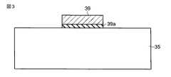
Next, a spin MOSFET using a laminate having a Heusler alloy according to a fourth embodiment of the present invention will be described. FIG. 5 is a cross-sectional view showing the structure of the spin MOSFET of the fourth embodiment.
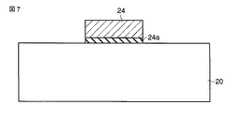
図5に示すように、半導体基板20上には、ソースまたはドレイン部としての非磁性金属アモルファス層21が形成されている。非磁性金属アモルファス層21上には、(001)配向したMgO層22が形成され、このMgO層22上にはエピタキシャル成長したホイスラー合金23が形成されている。さらに、ソースとドレインとの間の半導体基板20上にはゲート絶縁膜24aが形成され、このゲート絶縁膜24a上にはゲート電極24が形成されている。 As shown in FIG. 5, a nonmagnetic metal amorphous layer 21 as a source or drain part is formed on a
なお、前述したソースおよびドレインは、図6に示すような埋め込み型で構成されていてもよい。図6は、第4実施形態の変形例の埋め込み型スピンMOSFETの構造を示す断面図である。図6に示すように、半導体基板25に加工された凹部(ソースまたはドレインが形成されるべき部分)には、非磁性金属アモルファス層26が形成されている。この非磁性金属アモルファス層26上には、(001)配向したMgO層27が形成され、MgO層27上にはエピタキシャル成長したホイスラー合金28が形成されている。さらに、ソースとドレインとの間の半導体基板25上にはゲート絶縁膜30aが形成され、このゲート絶縁膜30a上にはゲート電極30が形成されている。ゲート電極30の側面には、側壁膜29が形成されている。 Note that the above-described source and drain may be of a buried type as shown in FIG. FIG. 6 is a cross-sectional view showing the structure of a buried spin MOSFET according to a modification of the fourth embodiment. As shown in FIG. 6, a nonmagnetic metal
次に、図5に示したスピンMOSFETの製造方法について説明する。まず、半導体基板20にイオン注入法およびアニールを用いてチャネル領域を形成した後、半導体基板20上に、例えばシリコン酸化膜24a及び多結晶シリコン膜24を順次形成する。次に、半導体基板20上において、ソースおよびドレインが形成される部分のシリコン酸化膜24a及び多結晶シリコン膜24をエッチングにより除去し、図7に示すように、ゲート絶縁膜24a及びゲート電極24を形成する。続いて、図5に示すように、ソースおよびドレインが形成される半導体基板20上に、非磁性金属アモルファス層21を形成する。この非磁性金属アモルファス層21上に、(001)配向したMgO層22を形成する。さらに、MgO層22上にエピタキシャル成長したホイスラー合金23を形成する。続いて、リフトオフ法またはイオンミリング法、RIE法などを用いて、非磁性金属アモルファス層21、MgO層22及びホイスラー合金23をパターニングしてソース電極及びドレイン電極を形成する。 Next, a method for manufacturing the spin MOSFET shown in FIG. 5 will be described. First, after forming a channel region in the
次に、図6に示したスピンMOSFETの製造方法について説明する。まず、半導体基板25にイオン注入法およびアニールを用いてチャネル領域を形成した後、半導体基板25上に、例えばシリコン酸化膜30a及び多結晶シリコン膜30を順次形成する。次に、半導体基板25上において、ソースおよびドレインが形成される部分のシリコン酸化膜30a及び多結晶シリコン膜30をエッチングにより除去し、図8に示すように、ゲート絶縁膜30a及びゲート電極30を形成する。続いて、半導体基板25上及びゲート電極30上に絶縁膜29を形成する。そして、この絶縁膜29をエッチバックしてゲート電極30の側面に側壁膜29を形成する。次に、半導体基板25において、ソースおよびドレインが形成される部分の半導体基板25をエッチングにより除去し、図9に示すように、半導体基板25に凹部を形成する。 Next, a method for manufacturing the spin MOSFET shown in FIG. 6 will be described. First, after forming a channel region in the
次に、図6に示すように、半導体基板25の凹部内に非磁性金属アモルファス層26を形成する。この非磁性金属アモルファス層26上に、(001)配向したMgO層27を形成する。さらに、MgO層27上に、エピタキシャル成長したホイスラー合金28を形成する。続いて、リフトオフ法またはイオンミリング法、RIE法などを用いて、非磁性金属アモルファス層26、MgO層27及びホイスラー合金28をパターニングしてソース電極及びドレイン電極を形成する。 Next, as shown in FIG. 6, a nonmagnetic metal
以上に説明した第3、第4実施形態において、非磁性金属アモルファス層17、21、26の材料としては、Er(エルビウム)、Yb(イッテルビウム)、Y(イットリウム)、Gd(ガドリウム)、Dy(ジスプロシウム)などの希土類元素や、Ag(銀)、Cu(銅)、Au(金)、Al(アルミニウム)、Ru(ルテニウム)、Ta(タンタル)、C(炭素)、Zr(ジリコニウム)、In(インジウム)、Ir(イリジウム)、W(タングステン)、Mo(モリブデン)、Pt(白金)、Ni(ニッケル)、Mg(マグネシウム)などの非磁性元素を用いることができる。 In the third and fourth embodiments described above, the materials of the nonmagnetic metal
第4実施形態のスピンMOSFETにおいては、ソース及びドレイン部から供給されるスピンを持ったキャリアは、バリア層であるMgO(001)層をトンネルすることによって伝導する。その際、前述した非磁性金属アモルファス層において、スピン緩和を小さくするために非磁性体を用いることにより、スピンMOSFETとして機能することが可能となる。 In the spin MOSFET of the fourth embodiment, carriers with spin supplied from the source and drain portions are conducted by tunneling through the MgO (001) layer that is a barrier layer. At this time, the nonmagnetic metal amorphous layer described above can function as a spin MOSFET by using a nonmagnetic material in order to reduce spin relaxation.
[第5実施形態]
次に、本発明の第5実施形態のホイスラー合金を有する積層体について説明する。図10は、第5実施形態のホイスラー合金を有する積層体の構造を示す断面図である。[Fifth Embodiment]
Next, the laminated body which has a Heusler alloy of 5th Embodiment of this invention is demonstrated. FIG. 10 is a cross-sectional view showing the structure of a laminate having a Heusler alloy according to the fifth embodiment.
第5実施形態の積層体は、図10に示すように、半導体基板または多結晶金属下地層1上に、絶縁体アモルファス層2、(001)配向したMgO層3、エピタキシャル成長したホイスラー合金4が順次積層された構造を有している。詳述すると、半導体基板または多結晶金属下地層1上には、絶縁体アモルファス層2が形成されている。この絶縁体アモルファス層2上には、(001)配向したMgO層3が形成されている。さらに、(001)配向したMgO層3上には、エピタキシャル成長したホイスラー合金4が形成されている。 In the laminated body of the fifth embodiment, as shown in FIG. 10, an insulator
第5実施形態の積層体においては、半導体基板または多結晶金属下地層1上に絶縁体アモルファス層2を形成し、この絶縁体アモルファス層2上にMgO層を形成すると、MgO層3は(001)配向して成長することを我々は見出した。さらに、ホイスラー合金4は、(001)配向したMgO層3上でエピタキシャル成長する。これにより、エピタキシャル成長したホイスラー合金4を、MgO層3上に形成することが可能である。以上により、半導体基板または多結晶金属下地層1上にエピタキシャル成長したホイスラー合金4を形成することが可能となる。 In the laminated body of the fifth embodiment, when the insulator
[第6実施形態]
次に、本発明の第6実施形態のホイスラー合金を有する積層体を用いたスピンMOSFETについて説明する。図11は、第6実施形態のスピンMOSFETの構造を示す断面図である。[Sixth Embodiment]
Next, a spin MOSFET using a stacked body having a Heusler alloy according to a sixth embodiment of the present invention will be described. FIG. 11 is a cross-sectional view showing the structure of the spin MOSFET of the sixth embodiment.
図11に示すように、半導体基板5上には、ソースまたはドレイン部としての絶縁体アモルファス層6が形成されている。絶縁体アモルファス層6上には、(001)配向したMgO層7が形成され、このMgO層7上にはエピタキシャル成長したホイスラー合金8が形成されている。さらに、ソースとドレインとの間の半導体基板5上にはゲート絶縁膜9aが形成され、このゲート絶縁膜9a上にはゲート電極9が形成されている。 As shown in FIG. 11, an insulating
なお、前述したソースおよびドレインは、図12に示すような埋め込み型で構成されていてもよい。図12は、第6実施形態の変形例の埋め込み型スピンMOSFETの構造を示す断面図である。図12に示すように、半導体基板10に加工された凹部(ソースまたはドレインが形成されるべき部分)には、絶縁体アモルファス層11が形成されている。この絶縁体アモルファス層11上には、(001)配向したMgO層12が形成されている。MgO層12上には、エピタキシャル成長したホイスラー合金13が形成されている。さらに、ソースとドレインとの間の半導体基板10上にはゲート絶縁膜14aが形成され、このゲート絶縁膜14a上にはゲート電極14が形成されている。ゲート電極14の側面には、側壁膜15が形成されている。 Note that the above-described source and drain may be of a buried type as shown in FIG. FIG. 12 is a cross-sectional view showing the structure of a buried spin MOSFET according to a modification of the sixth embodiment. As shown in FIG. 12, an insulator
次に、図11に示したスピンMOSFETの製造方法について説明する。まず、半導体基板5にイオン注入法およびアニールを用いてチャネル領域を形成した後、半導体基板5上に、例えばシリコン酸化膜9a及び多結晶シリコン膜9を順次形成する。次に、半導体基板5上において、ソースおよびドレインが形成される部分のシリコン酸化膜9a及び多結晶シリコン膜9をエッチングにより除去し、図13に示すように、ゲート絶縁膜9a及びゲート電極9を形成する。続いて、図11に示すように、ソースおよびドレインが形成される半導体基板5上に、絶縁体アモルファス層6を形成する。この絶縁体アモルファス層6上に、(001)配向したMgO層7を形成する。さらに、MgO層7上にエピタキシャル成長したホイスラー合金8を形成する。続いて、リフトオフ法またはイオンミリング法、RIE法などを用いて、絶縁体アモルファス層6、MgO層7及びホイスラー合金8をパターニングしてソース電極及びドレイン電極を形成する。 Next, a method for manufacturing the spin MOSFET shown in FIG. 11 will be described. First, after forming a channel region in the
次に、図12に示したスピンMOSFETの製造方法について説明する。まず、半導体基板10にイオン注入法およびアニールを用いてチャネル領域を形成した後、半導体基板10上に、例えばシリコン酸化膜14a及び多結晶シリコン膜14を順次形成する。次に、半導体基板10上において、ソースおよびドレインが形成される部分のシリコン酸化膜14a及び多結晶シリコン膜14をエッチングにより除去し、図14に示すように、ゲート絶縁膜14a及びゲート電極14を形成する。続いて、半導体基板10上及びゲート電極14上に絶縁膜15を形成する。そして、この絶縁膜15をエッチバックしてゲート電極14の側面に側壁膜15を形成する。次に、半導体基板10において、ソースおよびドレインが形成される部分の半導体基板10をエッチングにより除去し、図15に示すように、半導体基板10に凹部を形成する。 Next, a method for manufacturing the spin MOSFET shown in FIG. 12 will be described. First, after forming a channel region in the
次に、図12に示すように、半導体基板10の凹部内に絶縁体アモルファス層11を形成する。この絶縁体アモルファス層11上に、(001)配向したMgO層12を形成する。さらに、MgO層12上に、エピタキシャル成長したホイスラー合金13を形成する。続いて、リフトオフ法またはイオンミリング法、RIE法などを用いて、絶縁体アモルファス層11、MgO層12及びホイスラー合金13をパターニングしてソース電極及びドレイン電極を形成する。 Next, as shown in FIG. 12, the insulator
以上に説明した第5、第6実施形態において、絶縁体アモルファス層2、6、11の材料としては、酸化マグネシウム、酸化シリコン、酸化アルミニウム、窒化アルミニウム、酸化ビスマス、フッ化マグネシウム、フッ化カルシウム、チタン酸ストロンチウム、ランタンアルミネート、酸化窒化アルミニウム、酸化ハフニウムなどの各種の絶縁体を用いることができる。 In the fifth and sixth embodiments described above, the insulator
バリア層となる絶縁体アモルファス層2、6、11とMgO(001)層3、7、12とを合わせた膜厚は、キャリアのスピン緩和が起こらず、かつキャリアがトンネル可能な膜厚が望ましく、スピン拡散長より十分小さい3nm以下が望ましい。 The total thickness of the insulator
前述した第6実施形態のスピンMOSFETでは、移動度を向上させるために絶縁体アモルファス層6、11は5nmより薄く、より好ましくは3nmより薄いことが好ましい。特に、情報書き込みにスピン注入法を用いる場合、トンネルバリアの破壊を防ぐために1.2nm以下の膜厚にする必要がある。 In the above-described spin MOSFET of the sixth embodiment, the insulator
[第7実施形態]
次に、本発明の第7実施形態のMRAMについて説明する。このMRAMにおけるメモリセルには、ホイスラー合金を有する積層体をMTJ(Magnetic tunnel junction)素子を用いている。図16は、第7実施形態のMRAMにおけるメモリセルの構造を示す断面図である。[Seventh Embodiment]
Next, an MRAM according to a seventh embodiment of the present invention will be described. In a memory cell in this MRAM, an MTJ (Magnetic tunnel junction) element is used as a stacked body having a Heusler alloy. FIG. 16 is a cross-sectional view showing the structure of a memory cell in the MRAM of the seventh embodiment.
第7実施形態のMRAMにおけるメモリセルは、図16に示すように、半導体基板40に形成されたトランジスタ上に、電極層、多結晶金属下地配線47、MTJ素子48、金属ビア(または金属ハードマスク)49を順次形成し、その上にビット線50を形成した構造を有している。 As shown in FIG. 16, the memory cell in the MRAM of the seventh embodiment includes an electrode layer, a polycrystalline
以下に、MRAMにおけるメモリセルの構造を詳述する。半導体基板40には素子分離領域41が形成され、素子分離領域41に挟まれた半導体基板にはソース領域またはドレイン領域42が形成されている。ソース領域とドレイン領域との間の半導体基板40上には、ゲート絶縁膜43が形成されている。さらに、このゲート絶縁膜43上には、ゲート電極44が形成されている。また、半導体基板40上には層間絶縁膜45が形成され、ソース領域またはドレイン領域42上の層間絶縁膜45内には、コンタクトプラグ46を介して第1配線M1、第2配線M2、第3配線M3が順次形成されている。第3配線M3上のコンタクトプラグ46上には、多結晶金属下地配線47が形成されている。この多結晶金属下地配線47上には、MTJ素子48が形成されている。さらに、MTJ素子48上には金属ビア(または金属ハードマスク)49が形成され、この金属ビア49上にはビット線50が形成されている。 Hereinafter, the structure of the memory cell in the MRAM will be described in detail. An
ここで、MTJ素子48は、多結晶金属下地配線47上に、アモルファス層(非磁性金属アモルファス層または絶縁体アモルファス層)51を形成し、(001)配向したMgO層52、エピタキシャル成長したホイスラー合金/トンネルバリア/ホイスラー合金を順次積層した構造を有している。 Here, in the
MTJ素子48の詳細な断面構造を図17(a)または図17(b)に示す。図17(a)に示すように、アモルファス層51上にはMgO層52が形成され、このMgO層52上には体心立方格子(bcc)構造を有する金属層(bcc下地層)53が形成されている。bcc下地層53上には、ホイスラー合金54、トンネルバリア層(例えば、MgO層)55、ホイスラー合金56、CoFe層57、反強磁性層58、キャップ層59が順次形成されている。また、MTJ素子48の他の断面構造は、図17(b)に示すように、アモルファス層51上には、MgO層52、bcc下地層53、ホイスラー合金54、トンネルバリア層(例えば、MgO層)55、ホイスラー合金56、CoFe層57、Ru層60、CoFe層61、反強磁性層58、キャップ層59が順次形成されている。 The detailed cross-sectional structure of the
ここでは、ホイスラー合金54の結晶性を向上させるため、(001)配向したMgO層52とエピタキシャル成長したホイスラー合金54との界面に、前述したように、体心立方格子(bcc)構造を有する金属層53を形成している。bcc構造を有する金属層53としては、Cr(クロム)、Fe(鉄)、V(バナジウム)、Nb(ニオブ)、Mo(モリブデン)、Ta(タンタル)、W(タングステン)、またはこれらの合金などを用いることができる。なお、体心立方格子構造を有する金属層53は必ず必要なものではなく、(001)配向したMgO層52上に直接、エピタキシャル成長したホイスラー合金54を形成してもよい。 Here, in order to improve the crystallinity of the
[第8実施形態]
次に、本発明の第8実施形態のTMRヘッドについて説明する。このTMRヘッドは、MTJ素子を用いて形成されており、ハードディスクドライブ(HDD)に使用される。図18(a)及び図18(b)は、第8実施形態のTMRヘッドの構造を示す断面図である。[Eighth Embodiment]
Next, a TMR head according to an eighth embodiment of the invention will be described. This TMR head is formed using an MTJ element and is used in a hard disk drive (HDD). 18A and 18B are cross-sectional views showing the structure of the TMR head of the eighth embodiment.
このTMRヘッドは、図18(a)または図18(b)に示すように、MTJ素子が下部電極層70と上部電極層79の間に配置された構造を有している。ここでMTJ素子は、下部電極70上にアモルファス層(非磁性金属アモルファス層または絶縁体アモルファス層)71、(001)配向したMgO層72、エピタキシャル成長したホイスラー合金73を順次積層した構造を有している。詳述すると、図18(a)に示すように、下部電極層(磁気シールド層)70上には、アモルファス層71、MgO層72、ホイスラー合金73、トンネルバリア層(例えば、MgO層)74、ホイスラー合金75、CoFe層76、反強磁性層77、キャップ層78が順次形成されている。さらに、キャップ層78上には、上部電極層(磁気シールド層)79が形成されている。 This TMR head has a structure in which an MTJ element is disposed between a
また、ホイスラー合金73の結晶性を向上させるため、図18(b)に示すように、(001)配向したMgO層72とエピタキシャル成長したホイスラー合金73との界面に体心立方格子(bcc)構造を有する金属層80を形成してもよい。bcc構造を有する金属層80としては、Cr(クロム)、Fe(鉄)、V(バナジウム)、Nb(ニオブ)、Mo(モリブデン)、Ta(タンタル)、W(タングステン)などを用いることができる。 Further, in order to improve the crystallinity of the Heusler alloy 73, as shown in FIG. 18B, a body-centered cubic lattice (bcc) structure is formed at the interface between the (001) -oriented MgO layer 72 and the epitaxially grown Heusler alloy 73. You may form the metal layer 80 which has. As the metal layer 80 having the bcc structure, Cr (chromium), Fe (iron), V (vanadium), Nb (niobium), Mo (molybdenum), Ta (tantalum), W (tungsten), or the like can be used. .
以上に説明した第7、第8実施形態においては、バリア層となる絶縁体アモルファス層51,71とMgO(001)層52,72とを合わせた膜厚は、キャリアのスピン緩和が起こらず、かつキャリアがトンネル可能な膜厚が望ましく、スピン拡散長より十分小さい3nm以下が望ましい。 In the seventh and eighth embodiments described above, the combined film thickness of the insulator
また、前述した各実施形態において、半導体基板は、Si単結晶、またはGe単結晶、Si-Ge単結晶を有する基板、またはSOI(Silicon on Insulator)基板からなる。また、絶縁体アモルファス層は、MgO、SiO2、Al2O3、AlN、BiO3、MgF2、CaF2、SrTiO3、LaAlO3、Al−N−O、HfOなどからなる。非磁性金属アモルファス層は、Er、Yb、Y、Gd、Dyなどの希土類元素や、Ag、Cu、Au、Al、Ru、Ta、C、Zr、In、Ir、W、Mo、Pt、Ni、Mgなどの非磁性元素からなる。In each of the embodiments described above, the semiconductor substrate is made of a Si single crystal, a Ge single crystal, a substrate having a Si—Ge single crystal, or an SOI (Silicon on Insulator) substrate. Further, the insulator amorphouslayer, MgO, SiO 2, Al 2 O 3, AlN, BiO 3,
以下、実施例を参照して本発明の実施形態をさらに詳細に説明する。 Hereinafter, embodiments of the present invention will be described in more detail with reference to examples.
(実施例1)
本発明の実施例1として、ホイスラー合金を有する積層体を作製した。その作製手順を以下に示す。図19は、実施例1のホイスラー合金を有する積層体の構造を示す断面図である。Example 1
As Example 1 of this invention, the laminated body which has a Heusler alloy was produced. The production procedure is shown below. FIG. 19 is a cross-sectional view showing the structure of the laminate having the Heusler alloy of Example 1.
(001)配向したシリコン半導体単結晶基板64上に、アモルファス層である自然酸化膜(SiO2)65が形成されている。シリコン基板64上の自然酸化膜65に対してスパッタクリーニングを行い、自然酸化膜65の表面をクリーニングする。次に、自然酸化膜65上に、スパッタ法によりMgO層66を厚さ5nm形成する。さらに、MgO層66上に、スパッタ法によりCo2FeAl0.5Si0.5からなるホイスラー合金67を厚さ10nm形成する。A natural oxide film (SiO2 ) 65 that is an amorphous layer is formed on a (001) -oriented silicon semiconductor
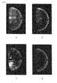
上記の手順で作製した実施例1の積層体において、電子線回折法により各層での反射高速電子回折(RHEED;Reflection High-Energy Electron Diffraction)像を観察した。図20(a)は自然酸化膜(SiO2)65のRHEED像を示し、図20(b)はMgO層66のRHEED像を、図20(c)はCo2FeAl0.5Si0.5ホイスラー合金67のRHEED像をそれぞれ示す。これらから判るように、図20(a)は、自然酸化膜65がアモルファス状態であることを示している。図20(b)は、自然酸化膜65上に形成されたMgO層66が(001)配向した構造を有していることを示している。さらに、図20(c)は、MgO層66上に形成されたCo2FeAl0.5Si0.5ホイスラー合金67がエピタキシャル成長した構造を有していることを示している。In the laminate of Example 1 produced by the above procedure, reflection high-energy electron diffraction (RHEED) images in each layer were observed by electron diffraction. 20A shows an RHEED image of the natural oxide film (SiO2 ) 65, FIG. 20B shows an RHEED image of the MgO layer 66, and FIG. 20C shows Co2 FeAl0.5 Si0.5. RHEED images of
従って、実施例1から半導体基板上に、エピタキシャル成長したホイスラー合金を形成することが可能であることがわかった。なお、実施例1では、半導体基板64上の自然酸化膜(SiO2)65膜上にMgO層66を介してホイスラー合金67を形成した場合を示したが、その他、半導体基板上のAl2OX膜上にMgO層を介してホイスラー合金を形成した場合でも同様の結果が得られた。また、半導体基板にイオン注入法、あるいはArなどを用いたイオンミリング法により不純物拡散層を形成した後、この不純物拡散層上にMgO層、ホイスラー合金を順次形成した場合でも、良好なMgO層、ホイスラー合金の積層膜が形成されることが明らかになった。Therefore, it was found from Example 1 that an epitaxially grown Heusler alloy can be formed on the semiconductor substrate. In Example 1, although the case of forming a
(実施例2)
本発明の実施例2として、図21に示すようなホイスラー合金を有する積層体を作製した。その作製手順を以下に示す。図21は、実施例2のホイスラー合金を有する積層体の構造を示す断面図である。(Example 2)
As Example 2 of this invention, the laminated body which has a Heusler alloy as shown in FIG. 21 was produced. The production procedure is shown below. FIG. 21 is a cross-sectional view showing the structure of the laminate having the Heusler alloy of Example 2.
まず、(001)配向したシリコン半導体単結晶基板81上の自然酸化膜をフッ酸処理によって除去する。次に、スパッタ法により希土類金属膜、例えばEr(エルビウム)82を厚さ3nm形成する。このEr82上にMgO層83を厚さ2nm形成し、さらにCo2FeAl0.5Si0.5ホイスラー合金84を厚さ10nm形成する。First, the natural oxide film on the (001) oriented silicon semiconductor
上記の手順で作製した実施例2の積層体において、電子線回折法により各層でのRHEED像を観察した。図22(a)は(001)配向したシリコン半導体基板81の表面のRHEED像を示し、図22(b)はEr82のRHEED像を、図22(c)はMgO層83のRHEED像を、図22(d)はCo2FeAl0.5Si0.5ホイスラー合金84のRHEED像をそれぞれ示す。これらから判るように、図22(a)は、(001)配向したシリコン半導体基板81の表面の結晶性が非常に高いことを示している。図22(b)は、(001)配向した半導体基板81上に形成されたEr82がアモルファス状態であることを示している。図22(c)は、Er82上に形成されたMgO層83が(001)配向した構造を有していることを示している。図22(d)は、MgO層83上に形成されたCo2FeAl0.5Si0.5ホイスラー合金84がエピタキシャル成長した構造を有していることを示している。In the laminate of Example 2 produced by the above procedure, RHEED images in each layer were observed by an electron beam diffraction method. 22A shows an RHEED image of the surface of the (001) -oriented
従って、実施例2から半導体基板上に、エピタキシャル成長したホイスラー合金を形成することが可能であることがわかった。なお、実施例2では、半導体基板81上に非磁性金属アモルファス層としてEr(エルビウム)82を形成し、Er(エルビウム)82上にMgO層83を介してホイスラー合金84を形成した場合を示したが、その他、半導体基板上に非磁性金属アモルファス層としてYb(イッテルビウム)、Y(イットリウム)などの希土類金属層を形成し、Yb(イッテルビウム)あるいはY(イットリウム)上にMgO層を介してホイスラー合金を形成した場合でも同様の結果が得られた。 Therefore, it was found from Example 2 that an epitaxially grown Heusler alloy can be formed on the semiconductor substrate. In the second embodiment, Er (erbium) 82 is formed as a nonmagnetic metal amorphous layer on the
本発明の実施形態によれば、ホイスラー合金を用いたスピンMOSFETを作製することが可能となり、高いTMR比をもつスピンMOSFETの実現に極めて有用である。 According to the embodiment of the present invention, a spin MOSFET using a Heusler alloy can be manufactured, which is extremely useful for realizing a spin MOSFET having a high TMR ratio.
また、前述した各実施形態はそれぞれ、単独で実施できるばかりでなく、適宜組み合わせて実施することも可能である。さらに、前述した各実施形態には種々の段階の発明が含まれており、各実施形態において開示した複数の構成要件の適宜な組み合わせにより、種々の段階の発明を抽出することも可能である。 In addition, each of the above-described embodiments can be implemented not only independently but also in an appropriate combination. Furthermore, the above-described embodiments include inventions at various stages, and the inventions at various stages can be extracted by appropriately combining a plurality of constituent elements disclosed in the embodiments.
1,16…半導体基板(または多結晶金属下地層)、2,6,11…絶縁体アモルファス層、3,7,12,18,22,27,33,37,52,66,72,83…MgO層、4,8,13,19,23,28,34,38,54,56,67,73,75,84…ホイスラー合金、5,10,20,25,31,35,40…半導体基板、9,14,24,30,39,44…ゲート電極、9a,14a,24a,30a,39a,43…ゲート絶縁膜、15,29…側壁膜、17,21,26…非磁性金属アモルファス層、32,36…不純物拡散層、41…素子分離領域、42…ソース領域またはドレイン領域、45…層間絶縁膜、46…コンタクトプラグ、47…多結晶金属下地配線、48…MTJ素子、49…金属ビア(または金属ハードマスク)、50…ビット線、51…アモルファス層、53…体心立方格子(bcc)構造を有する金属層(bcc下地層)、55…トンネルバリア層(例えば、MgO層)、57…CoFe層、58…反強磁性層、59…キャップ層、60…Ru層、61…CoFe層、64,81…シリコン半導体単結晶基板、65…自然酸化膜(SiO2)、70…下部電極層(磁気シールド層)、71…アモルファス層、74…トンネルバリア層(例えば、MgO層)、76…CoFe層、77…反強磁性層、78…キャップ層、79…上部電極層(磁気シールド層)、80…体心立方格子(bcc)構造を有する金属層、82…Er(エルビウム)、M1…第1配線、M2…第2配線、M3…第3配線。DESCRIPTION OF
Claims (12)
Translated fromJapanese前記非磁性金属アモルファス層上に形成され、(001)配向したMgO層と、
前記MgO層上に形成され、エピタキシャル成長したホイスラー合金と、
を積層した構造を有することを特徴とする積層体。A non-magnetic metal amorphous layer formed on the semiconductor layer;
A (001) -oriented MgO layer formed on the non-magnetic metal amorphous layer;
An Heusler alloy epitaxially grown on the MgO layer;
A laminated body characterized by having a structure in which layers are laminated.
前記非磁性金属アモルファス層上に形成され、(001)配向したMgO層と、
前記MgO層上に形成され、エピタキシャル成長したホイスラー合金と、
を積層した構造を有するソース及びドレイン電極を具備することを特徴とするスピンMOS電界効果トランジスタ。A non-magnetic metal amorphous layer formed on the semiconductor layer;
A (001) -oriented MgO layer formed on the non-magnetic metal amorphous layer;
An Heusler alloy epitaxially grown on the MgO layer;
A spin MOS field effect transistor comprising a source electrode and a drain electrode having a stacked structure.
前記MgO層上に形成され、エピタキシャル成長したホイスラー合金と、
を積層した構造を有し、
前記絶縁体アモルファス層は、酸化シリコン、酸化アルミニウム、窒化アルミニウム、酸化ビスマス、フッ化マグネシウム、フッ化カルシウム、チタン酸ストロンチウム、ランタンアルミネート、酸化窒化アルミニウム、酸化ハフニウムの少なくともいずれかを含むことを特徴とする積層体。A tunnel barrier layer having an insulator amorphous layer formed on the semiconductor layer and a (001) -oriented MgO layer formed on the insulator amorphous layer;
An Heusler alloy epitaxially grown on the MgO layer;
Have a laminatedstructure,
The insulator amorphous layer includes at least one of silicon oxide, aluminum oxide, aluminum nitride, bismuth oxide, magnesium fluoride, calcium fluoride, strontium titanate, lanthanum aluminate, aluminum oxynitride, and hafnium oxide. Laminated body.
前記MgO層上に形成され、エピタキシャル成長したホイスラー合金と、
を積層した構造を有するソース及びドレイン電極を具備し、
前記絶縁体アモルファス層は、酸化シリコン、酸化アルミニウム、窒化アルミニウム、酸化ビスマス、フッ化マグネシウム、フッ化カルシウム、チタン酸ストロンチウム、ランタンアルミネート、酸化窒化アルミニウム、酸化ハフニウムの少なくともいずれかを含むことを特徴とするスピンMOS電界効果トランジスタ。A tunnel barrier layer having an insulator amorphous layer formed on the semiconductor layer and a (001) -oriented MgO layer formed on the insulator amorphous layer;
An Heusler alloy epitaxially grown on the MgO layer;
Was provided with source and drain electrodes having a structurelaminated,
The insulator amorphous layer includes at least one of silicon oxide, aluminum oxide, aluminum nitride, bismuth oxide, magnesium fluoride, calcium fluoride, strontium titanate, lanthanum aluminate, aluminum oxynitride, and hafnium oxide. Spin MOS field effect transistor.
前記非磁性金属アモルファス層上に形成され、(001)配向したMgO層と、
前記MgO層上に形成され、エピタキシャル成長したホイスラー合金と、
を積層した構造を有することを特徴とする積層体。A non-magnetic metal amorphous layer formed on the polycrystalline metal layer;
A (001) -oriented MgO layer formed on the non-magnetic metal amorphous layer;
An Heusler alloy epitaxially grown on the MgO layer;
A laminated body characterized by having a structure in which layers are laminated.
前記非磁性金属アモルファス層上に形成され、(001)配向したMgO層と、
前記MgO層上に形成され、エピタキシャル成長したホイスラー合金からなる第1強磁性層と、
前記第1強磁性層上に形成されたトンネルバリア層と、
前記トンネルバリア層上に形成された第2強磁性層と、
を積層した構造を有することを特徴とするトンネル磁気抵抗効果(TMR:Tunneling Magneto Resistance effect)素子。A non-magnetic metal amorphous layer formed on the electrode layer;
A (001) -oriented MgO layer formed on the non-magnetic metal amorphous layer;
A first ferromagnetic layer formed on the MgO layer and made of an epitaxially grown Heusler alloy;
A tunnel barrier layer formed on the first ferromagnetic layer;
A second ferromagnetic layer formed on the tunnel barrier layer;
A tunneling magnetoresistive effect (TMR) element characterized by having a laminated structure.
前記絶縁体アモルファス層上に形成され、(001)配向したMgO層と、
前記MgO層上に形成され、エピタキシャル成長したホイスラー合金からなる第1強磁性層と、
前記第1強磁性層上に形成されたトンネルバリア層と、
前記トンネルバリア層上に形成された第2強磁性層と、
を積層した構造を有し、
前記絶縁体アモルファス層は、酸化シリコン、酸化アルミニウム、窒化アルミニウム、酸化ビスマス、フッ化マグネシウム、フッ化カルシウム、チタン酸ストロンチウム、ランタンアルミネート、酸化窒化アルミニウム、酸化ハフニウムの少なくともいずれかを含むことを特徴とするトンネル磁気抵抗効果(TMR:Tunneling Magneto Resistance effect)素子。An insulator amorphous layer formed on the electrode layer;
An (001) oriented MgO layer formed on the insulator amorphous layer;
A first ferromagnetic layer formed on the MgO layer and made of an epitaxially grown Heusler alloy;
A tunnel barrier layer formed on the first ferromagnetic layer;
A second ferromagnetic layer formed on the tunnel barrier layer;
Have a laminatedstructure,
The insulator amorphous layer includes at least one of silicon oxide, aluminum oxide, aluminum nitride, bismuth oxide, magnesium fluoride, calcium fluoride, strontium titanate, lanthanum aluminate, aluminum oxynitride, and hafnium oxide. A tunneling magneto-resistance effect (TMR) element.
Priority Applications (3)
| Application Number | Priority Date | Filing Date | Title |
|---|---|---|---|
| JP2007218963AJP4580966B2 (en) | 2007-08-24 | 2007-08-24 | Laminated body having Heusler alloy, spin MOS field effect transistor and tunnel magnetoresistive element using the laminated body |
| US12/194,797US7709867B2 (en) | 2007-08-24 | 2008-08-20 | Spin MOS field effect transistor and tunneling magnetoresistive effect element using stack having Heusler alloy |
| US12/662,100US7943974B2 (en) | 2007-08-24 | 2010-03-31 | Spin MOS field effect transistor and tunneling magnetoresistive effect element using stack having Heusler alloy |
Applications Claiming Priority (1)
| Application Number | Priority Date | Filing Date | Title |
|---|---|---|---|
| JP2007218963AJP4580966B2 (en) | 2007-08-24 | 2007-08-24 | Laminated body having Heusler alloy, spin MOS field effect transistor and tunnel magnetoresistive element using the laminated body |
Publications (2)
| Publication Number | Publication Date |
|---|---|
| JP2009054724A JP2009054724A (en) | 2009-03-12 |
| JP4580966B2true JP4580966B2 (en) | 2010-11-17 |
Family
ID=40381349
Family Applications (1)
| Application Number | Title | Priority Date | Filing Date |
|---|---|---|---|
| JP2007218963AExpired - Fee RelatedJP4580966B2 (en) | 2007-08-24 | 2007-08-24 | Laminated body having Heusler alloy, spin MOS field effect transistor and tunnel magnetoresistive element using the laminated body |
Country Status (2)
| Country | Link |
|---|---|
| US (2) | US7709867B2 (en) |
| JP (1) | JP4580966B2 (en) |
Families Citing this family (30)
| Publication number | Priority date | Publication date | Assignee | Title |
|---|---|---|---|---|
| JP4996390B2 (en)* | 2007-08-28 | 2012-08-08 | 株式会社東芝 | Spin FET and magnetoresistance effect element |
| JP4703660B2 (en)* | 2008-01-11 | 2011-06-15 | 株式会社東芝 | Spin MOS field effect transistor |
| JP4762285B2 (en)* | 2008-09-24 | 2011-08-31 | 株式会社東芝 | Spin transistor, integrated circuit, and magnetic memory |
| JP4764466B2 (en) | 2008-09-25 | 2011-09-07 | 株式会社東芝 | Laminated body having Heusler alloy, magnetoresistive element using this laminated body, and spin transistor |
| JP2010239011A (en)* | 2009-03-31 | 2010-10-21 | Tdk Corp | Spin injection structure and spin conduction device using the same |
| JP2010238956A (en)* | 2009-03-31 | 2010-10-21 | Tdk Corp | Spin conductive device |
| WO2010119928A1 (en) | 2009-04-16 | 2010-10-21 | 独立行政法人物質・材料研究機構 | Ferromagnetic tunnel junction structure, and magnetoresistive effect element and spintronics device each comprising same |
| JP5527669B2 (en)* | 2009-05-22 | 2014-06-18 | 独立行政法人物質・材料研究機構 | Ferromagnetic tunnel junction and magnetoresistive effect element using the same |
| JP5326841B2 (en)* | 2009-06-10 | 2013-10-30 | Tdk株式会社 | Spin transport element |
| US8507966B2 (en) | 2010-03-02 | 2013-08-13 | Micron Technology, Inc. | Semiconductor cells, arrays, devices and systems having a buried conductive line and methods for forming the same |
| US9608119B2 (en)* | 2010-03-02 | 2017-03-28 | Micron Technology, Inc. | Semiconductor-metal-on-insulator structures, methods of forming such structures, and semiconductor devices including such structures |
| US9646869B2 (en) | 2010-03-02 | 2017-05-09 | Micron Technology, Inc. | Semiconductor devices including a diode structure over a conductive strap and methods of forming such semiconductor devices |
| US8288795B2 (en) | 2010-03-02 | 2012-10-16 | Micron Technology, Inc. | Thyristor based memory cells, devices and systems including the same and methods for forming the same |
| JP5161951B2 (en) | 2010-11-26 | 2013-03-13 | 株式会社東芝 | Spin torque oscillator and magnetic recording apparatus |
| US9166004B2 (en)* | 2010-12-23 | 2015-10-20 | Intel Corporation | Semiconductor device contacts |
| US9277872B2 (en) | 2011-01-13 | 2016-03-08 | Rhythmia Medical, Inc. | Electroanatomical mapping |
| US9002442B2 (en) | 2011-01-13 | 2015-04-07 | Rhythmia Medical, Inc. | Beat alignment and selection for cardiac mapping |
| US8952418B2 (en) | 2011-03-01 | 2015-02-10 | Micron Technology, Inc. | Gated bipolar junction transistors |
| US8519431B2 (en) | 2011-03-08 | 2013-08-27 | Micron Technology, Inc. | Thyristors |
| JP5677347B2 (en)* | 2012-03-22 | 2015-02-25 | 株式会社東芝 | Magnetoresistive element and magnetic memory writing method |
| JP5959313B2 (en)* | 2012-05-28 | 2016-08-02 | 三菱電機株式会社 | Magnetoresistive element, magnetic field detector and physical quantity detector |
| JP6148450B2 (en)* | 2012-10-29 | 2017-06-14 | 株式会社東芝 | Stacked structure, spin transistor and reconfigurable logic circuit |
| US9166152B2 (en) | 2012-12-22 | 2015-10-20 | Samsung Electronics Co., Ltd. | Diffusionless transformations in MTJ stacks |
| WO2014163121A1 (en)* | 2013-04-05 | 2014-10-09 | 独立行政法人物質・材料研究機構 | Current-perpendicular-to-plane magneto-resistance effect element |
| KR20140134068A (en)* | 2013-05-13 | 2014-11-21 | 에스케이하이닉스 주식회사 | Spin transistor, and semiconductor device, memory device, microprocessor, processor, system, data storage system and memory system including the spin transistor |
| KR102124361B1 (en)* | 2013-11-18 | 2020-06-19 | 삼성전자주식회사 | Magnetic memory devices having perpendicular magnetic tunnel junction |
| CN105745761B (en)* | 2013-11-20 | 2019-04-09 | Tdk株式会社 | Magnetoresistive effect elements, spin MOSFETs and spin conduction elements |
| WO2017053921A1 (en) | 2015-09-26 | 2017-03-30 | Boston Scientific Scimed Inc. | Intracardiac egm signals for beat matching and acceptance |
| JP6754108B2 (en)* | 2015-12-04 | 2020-09-09 | 国立研究開発法人物質・材料研究機構 | Single crystal magnetoresistive sensor, its manufacturing method and its usage |
| US10396123B2 (en)* | 2017-07-26 | 2019-08-27 | International Business Machines Corporation | Templating layers for perpendicularly magnetized Heusler films |
Family Cites Families (11)
| Publication number | Priority date | Publication date | Assignee | Title |
|---|---|---|---|---|
| JPS6311659A (en)* | 1986-06-30 | 1988-01-19 | Matsushita Electric Ind Co Ltd | Magneto-optical material |
| JP4304568B2 (en)* | 2002-04-23 | 2009-07-29 | 独立行政法人産業技術総合研究所 | Flattened tunnel magnetoresistive element |
| JP2003115623A (en)* | 2001-06-04 | 2003-04-18 | Matsushita Electric Ind Co Ltd | Magnetoresistance element, magnetoresistance storage element, and magnetic memory |
| US7411235B2 (en)* | 2004-06-16 | 2008-08-12 | Kabushiki Kaisha Toshiba | Spin transistor, programmable logic circuit, and magnetic memory |
| JP4528660B2 (en)* | 2005-03-31 | 2010-08-18 | 株式会社東芝 | Spin injection FET |
| JP4599259B2 (en)* | 2005-09-20 | 2010-12-15 | 株式会社東芝 | Magnetic element and magnetic signal processing apparatus using the same |
| JP2007189039A (en)* | 2006-01-13 | 2007-07-26 | Alps Electric Co Ltd | Tunnel-type magnetic sensing element and manufacturing method thereof |
| JP4582488B2 (en)* | 2006-04-27 | 2010-11-17 | 独立行政法人科学技術振興機構 | Magnetic thin film, magnetoresistive effect element and magnetic device using the same |
| JP2008218641A (en)* | 2007-03-02 | 2008-09-18 | Tohoku Univ | Tunnel magnetoresistive element |
| JP4996390B2 (en)* | 2007-08-28 | 2012-08-08 | 株式会社東芝 | Spin FET and magnetoresistance effect element |
| JP4703660B2 (en)* | 2008-01-11 | 2011-06-15 | 株式会社東芝 | Spin MOS field effect transistor |
- 2007
- 2007-08-24JPJP2007218963Apatent/JP4580966B2/ennot_activeExpired - Fee Related
- 2008
- 2008-08-20USUS12/194,797patent/US7709867B2/enactiveActive
- 2010
- 2010-03-31USUS12/662,100patent/US7943974B2/enactiveActive
Also Published As
| Publication number | Publication date |
|---|---|
| JP2009054724A (en) | 2009-03-12 |
| US7943974B2 (en) | 2011-05-17 |
| US7709867B2 (en) | 2010-05-04 |
| US20100187585A1 (en) | 2010-07-29 |
| US20090050948A1 (en) | 2009-02-26 |
Similar Documents
| Publication | Publication Date | Title |
|---|---|---|
| JP4580966B2 (en) | Laminated body having Heusler alloy, spin MOS field effect transistor and tunnel magnetoresistive element using the laminated body | |
| JP4703660B2 (en) | Spin MOS field effect transistor | |
| US9780300B2 (en) | Magnetic memory element with composite perpendicular enhancement layer | |
| US11087810B2 (en) | Free layer structure in magnetic random access memory (MRAM) for Mo or W perpendicular magnetic anisotropy (PMA) enhancing layer | |
| US7352021B2 (en) | Magnetic random access memory devices having titanium-rich lower electrodes with oxide layer and oriented tunneling barrier | |
| US20180076384A1 (en) | Magnetic random access memory with perpendicular enhancement layer | |
| JP6180972B2 (en) | Magnetoresistive element and magnetic memory | |
| KR101929583B1 (en) | Nonvolatile magnetic memory device | |
| US20140217526A1 (en) | Novel perpendicular magnetoresistive elements | |
| JP2012182217A (en) | Semiconductor storage device | |
| JP2007305610A (en) | Tunnel magnetoresistive element, nonvolatile magnetic memory, light emitting element, and three-terminal element | |
| US20220238799A1 (en) | Magnetoresistive element having a composite recording structure | |
| US10672977B2 (en) | Perpendicular magnetoresistive elements | |
| US20230039108A1 (en) | Perpendicular mtj element having a soft-magnetic adjacent layer and methods of making the same | |
| US11043631B2 (en) | Perpendicular magnetoresistive elements | |
| JP2009239122A (en) | Magneto-resistance effect device and spin mos (metal oxide semiconductor) field-effect transistor | |
| JP5377531B2 (en) | Spin MOS field effect transistor | |
| US11910721B2 (en) | Perpendicular MTJ element having a cube-textured reference layer and methods of making the same | |
| US20220246836A1 (en) | Composite recording structure for an improved write profermance | |
| JP5072877B2 (en) | Spin transistor | |
| WO2011062005A1 (en) | Ferromagnetic tunnel junction element |
Legal Events
| Date | Code | Title | Description |
|---|---|---|---|
| A977 | Report on retrieval | Free format text:JAPANESE INTERMEDIATE CODE: A971007 Effective date:20090710 | |
| A131 | Notification of reasons for refusal | Free format text:JAPANESE INTERMEDIATE CODE: A131 Effective date:20090721 | |
| A521 | Request for written amendment filed | Free format text:JAPANESE INTERMEDIATE CODE: A523 Effective date:20090924 | |
| A02 | Decision of refusal | Free format text:JAPANESE INTERMEDIATE CODE: A02 Effective date:20100302 | |
| A521 | Request for written amendment filed | Free format text:JAPANESE INTERMEDIATE CODE: A523 Effective date:20100602 | |
| A911 | Transfer to examiner for re-examination before appeal (zenchi) | Free format text:JAPANESE INTERMEDIATE CODE: A911 Effective date:20100609 | |
| TRDD | Decision of grant or rejection written | ||
| A01 | Written decision to grant a patent or to grant a registration (utility model) | Free format text:JAPANESE INTERMEDIATE CODE: A01 Effective date:20100803 | |
| A01 | Written decision to grant a patent or to grant a registration (utility model) | Free format text:JAPANESE INTERMEDIATE CODE: A01 | |
| A61 | First payment of annual fees (during grant procedure) | Free format text:JAPANESE INTERMEDIATE CODE: A61 Effective date:20100830 | |
| FPAY | Renewal fee payment (event date is renewal date of database) | Free format text:PAYMENT UNTIL: 20130903 Year of fee payment:3 | |
| FPAY | Renewal fee payment (event date is renewal date of database) | Free format text:PAYMENT UNTIL: 20130903 Year of fee payment:3 | |
| LAPS | Cancellation because of no payment of annual fees |