JP4578329B2 - Semiconductor memory device - Google Patents
Semiconductor memory deviceDownload PDFInfo
- Publication number
- JP4578329B2 JP4578329B2JP2005163641AJP2005163641AJP4578329B2JP 4578329 B2JP4578329 B2JP 4578329B2JP 2005163641 AJP2005163641 AJP 2005163641AJP 2005163641 AJP2005163641 AJP 2005163641AJP 4578329 B2JP4578329 B2JP 4578329B2
- Authority
- JP
- Japan
- Prior art keywords
- wiring
- power supply
- memory cell
- metal
- line
- Prior art date
- Legal status (The legal status is an assumption and is not a legal conclusion. Google has not performed a legal analysis and makes no representation as to the accuracy of the status listed.)
- Expired - Fee Related
Links
Images


Classifications
- H—ELECTRICITY
- H10—SEMICONDUCTOR DEVICES; ELECTRIC SOLID-STATE DEVICES NOT OTHERWISE PROVIDED FOR
- H10B—ELECTRONIC MEMORY DEVICES
- H10B10/00—Static random access memory [SRAM] devices
- H10B10/12—Static random access memory [SRAM] devices comprising a MOSFET load element
- G—PHYSICS
- G11—INFORMATION STORAGE
- G11C—STATIC STORES
- G11C11/00—Digital stores characterised by the use of particular electric or magnetic storage elements; Storage elements therefor
- G11C11/21—Digital stores characterised by the use of particular electric or magnetic storage elements; Storage elements therefor using electric elements
- G11C11/34—Digital stores characterised by the use of particular electric or magnetic storage elements; Storage elements therefor using electric elements using semiconductor devices
- G11C11/40—Digital stores characterised by the use of particular electric or magnetic storage elements; Storage elements therefor using electric elements using semiconductor devices using transistors
- G11C11/41—Digital stores characterised by the use of particular electric or magnetic storage elements; Storage elements therefor using electric elements using semiconductor devices using transistors forming static cells with positive feedback, i.e. cells not needing refreshing or charge regeneration, e.g. bistable multivibrator or Schmitt trigger
- G11C11/412—Digital stores characterised by the use of particular electric or magnetic storage elements; Storage elements therefor using electric elements using semiconductor devices using transistors forming static cells with positive feedback, i.e. cells not needing refreshing or charge regeneration, e.g. bistable multivibrator or Schmitt trigger using field-effect transistors only
- G—PHYSICS
- G11—INFORMATION STORAGE
- G11C—STATIC STORES
- G11C5/00—Details of stores covered by group G11C11/00
- G11C5/14—Power supply arrangements, e.g. power down, chip selection or deselection, layout of wirings or power grids, or multiple supply levels
- H—ELECTRICITY
- H10—SEMICONDUCTOR DEVICES; ELECTRIC SOLID-STATE DEVICES NOT OTHERWISE PROVIDED FOR
- H10B—ELECTRONIC MEMORY DEVICES
- H10B10/00—Static random access memory [SRAM] devices
Landscapes
- Engineering & Computer Science (AREA)
- Microelectronics & Electronic Packaging (AREA)
- Computer Hardware Design (AREA)
- Power Engineering (AREA)
- Semiconductor Memories (AREA)
Description
Translated fromJapaneseこの発明は、半導体記憶装置に関し、特に、メモリセルがフリップフロップ構成を備えるスタティック型半導体記憶装置に関する。より特定的には、この発明は、スタティック型半導体記憶装置の消費電力を低減するためのメモリセルのレイアウトに関する。 The present invention relates to a semiconductor memory device, and more particularly to a static semiconductor memory device in which a memory cell has a flip-flop configuration. More specifically, the present invention relates to a memory cell layout for reducing power consumption of a static semiconductor memory device.
微細化技術の進展に伴って、システムLSI(大規模集積回路)またはシステム・オン・チップ(SOC)などと呼ばれる高機能の半導体集積回路装置が実現されている。このような半導体集積回路装置においては、プロセッサなどの処理を実行するロジック回路と、このロジック回路が使用するデータおよびプログラム情報を格納するメモリとが同一半導体チップ上に集積化される。このような大規模集積回路装置は、画像処理または通信処理などにおいて用いられている。画像処理および通信処理においては、高速で大量のデータを処理することが要求され、この集積回路装置内に搭載されるメモリに対しても、その記憶容量を大きくすることが要求される。 Along with the progress of miniaturization technology, highly functional semiconductor integrated circuit devices called system LSI (large scale integrated circuit) or system on chip (SOC) have been realized. In such a semiconductor integrated circuit device, a logic circuit that executes processing such as a processor and a memory that stores data and program information used by the logic circuit are integrated on the same semiconductor chip. Such a large-scale integrated circuit device is used in image processing or communication processing. In image processing and communication processing, it is required to process a large amount of data at high speed, and it is also required to increase the storage capacity of the memory mounted in the integrated circuit device.
メモリ(半導体記憶装置)の記憶容量を増大する場合、コスト上昇の抑制および前世代装置との互換性等の観点から、チップレイアウト面積を増大させることなく、高密度でメモリセルを配置することが要求される。メモリセルを高密度に配置するために、メモリセルトランジスタを配置する基板領域(ウェル領域)を、列方向に直線的に延在させ、メモリセルの拡散領域を直線的な矩形形状に配設する構成が、特許文献1(特開2002−043441号公報)、特許文献2(特開2003−297953号公報)、特許文献3(特開2003−060089号公報)、および特許文献4(特開2001−028401号公報)において示されている。 When increasing the storage capacity of a memory (semiconductor memory device), it is possible to arrange memory cells at a high density without increasing the chip layout area from the viewpoint of suppressing cost increase and compatibility with the previous generation device. Required. In order to arrange memory cells at high density, a substrate region (well region) on which memory cell transistors are arranged extends linearly in the column direction, and a diffusion region of the memory cells is arranged in a linear rectangular shape. The configuration is described in Japanese Patent Application Laid-Open No. 2002-043441, Japanese Patent Application Laid-Open No. 2003-297953, Japanese Patent Application Laid-Open No. 2003-060089, and Japanese Patent Application Laid-Open No. 2003-060089. -0284401).
これらの特許文献1から4に示されるメモリセルのレイアウトにおいては、Pウェル内にnチャネルMOSトランジスタ(絶縁ゲート型電界効果トランジスタ)で構成されるアクセストランジスタやおよびドライバトランジスタを配置し、このPウェルに隣接して形成されるNウェル内に、pチャネルMOSトランジスタで構成される負荷トランジスタが配置される。ビット線、電源線、および接地線が、列方向に各ウェル領域と平行に配設され、電源線および接地線がそれぞれ、対応の列のメモリセルの負荷トランジスタソースノードおよびドライバトランジスタソースノードに結合される。ウェル領域を直線的に延在させて配線レイアウトを容易としかつ微細化を可能とするとともに、トランジスタのゲート長またはメモリセルのアクセストランジスタとビット線との間の距離を短くして、配線抵抗を低減することを図る。 In the memory cell layouts shown in these Patent Documents 1 to 4, an access transistor and a driver transistor composed of n-channel MOS transistors (insulated gate field effect transistors) are arranged in a P well, and the P well A load transistor formed of a p-channel MOS transistor is arranged in an N well formed adjacent to the N channel. A bit line, a power supply line, and a ground line are arranged in the column direction in parallel with each well region, and the power supply line and the ground line are respectively coupled to the load transistor source node and the driver transistor source node of the memory cell in the corresponding column. Is done. The well region is extended linearly to facilitate wiring layout and miniaturization, while reducing the gate length of the transistor or the distance between the access transistor of the memory cell and the bit line, thereby reducing the wiring resistance. Try to reduce.
大記憶容量のメモリ装置を実現する場合、発熱および電池寿命(携帯機器用途の場合)などの観点から、消費電力をできるだけ抑制することが要求される。スタンバイ時の消費電流および動作時の消費電力を電源することを図る構成が、非特許文献1(信学技報、第104巻、第66号、「高集積・低電力を実現した90nmテクノロジーのSoC向けデュアルポートSRAMの開発」、ニイ等)および非特許文献2(ISCC2004、ダイジェスト・オブ・テクニカルペーパーズ、ニイ等、「ダイナミック制御型コラムバイアス方式を用いた2.04μm2 8T薄膜セルを用いた90nmデュアルポートSRAM"A 90 nm Dual-Port SRAM with 2.04um2 8T-Thin Cell Using Dynamically-Controlled Column Bias Scheme"」)において示されている。When realizing a memory device with a large storage capacity, it is required to suppress power consumption as much as possible from the viewpoint of heat generation and battery life (for portable equipment). Non-Patent Document 1 (Science Technical Report, Vol. 104, No. 66, “The 90 nm technology that achieves high integration and low power” has been proposed to supply power consumption during standby and power consumption during operation. use development of SoC for dual-port SRAM ", Nii, etc.) and non-patent literature 2 (ISCC2004, digest of Technical papers, Nii, etc., the 2.04μm2 8T thin film cell using a" dynamic control type
これらの非特許文献1および2は、同一の内容を開示しており、デュアルポートSRAMにおいて、メモリセル列単位でドライバトランジスタに結合されるソース線(接地線)の電圧を制御する。すなわち、非選択メモリセル列のドライバトランジスタのソース電圧VSLは、たとえば0.4Vの高い電圧レベルに設定し、一方、選択列のメモリセルのドライバトランジスタのソース電圧は、接地電圧レベルに駆動される。非選択メモリセルのドライバトランジスタのゲート−ソース間バイアスを、逆バイアス状態として、より深いオフ状態とし、サブスレッショルドリーク電流およびゲートリーク電流を低減し、応じてスタンバイ時の消費電流を低減する。 These Non-Patent Documents 1 and 2 disclose the same contents, and control the voltage of a source line (ground line) coupled to a driver transistor in units of memory cell columns in a dual port SRAM. That is, the source voltage VSL of the driver transistor in the non-selected memory cell column is set to a high voltage level of, for example, 0.4 V, while the source voltage of the driver transistor in the memory cell in the selected column is driven to the ground voltage level. . The gate-source bias of the driver transistor of the non-selected memory cell is set in a reverse bias state to a deeper off state, thereby reducing the subthreshold leakage current and the gate leakage current, and correspondingly reducing the current consumption during standby.
選択列かつ選択行のメモリセルは、ドライバトランジスタのソース線が接地電圧レベルであり、読出時、ビット線電位を記憶データに応じて放電する。選択列かつ非選択行のメモリセルにおいては、カラム電流よりも小さなリーク電流が流れるだけであり、動作電流に比べてほぼ無視することができる。さらに、選択行かつ非選択列のメモリセルにおいては、ドライバトランジスタがゲート−ソース間が逆バイアス状態に設定されており、ビット線の放電はほとんど行なわれず、カラム電流が抑制され、動作時の消費電流が低減される。
特許文献1、2および4に示される構成の配線レイアウトにおいては、メモリセル領域の中央部に、電源線が配置され、ビット線外部に、接地線が配置される。したがって、接地線は隣接列のメモリセルにより共有されており、各列単位で、接地電圧の制御を行なうことができず、スタンバイ電流および動作電流を低減するという上述の非特許文献1および2の構成を適用することができない。 In the wiring layout having the configuration shown in Patent Documents 1, 2, and 4, a power supply line is arranged at the center of the memory cell region, and a ground line is arranged outside the bit line. Therefore, the ground line is shared by memory cells in adjacent columns, and the ground voltage cannot be controlled in units of each column, and the standby current and the operating current are reduced as described in Non-Patent Documents 1 and 2 above. The configuration cannot be applied.
特許文献3においては、図7において、メモリセル中央部に接地線を配置し、ビット線外部に電源線を配置する配線レイアウトが示されている。この配線レイアウトでは、接地線が各列単位で配置されており、接地線を各列毎にその電位を調整することが可能である。しかしながら、メモリセル領域中央部に配置されるPウェルにおいて、2つのアクセストランジスタおよび2つのドライバトランジスタを形成する活性領域を、列方向に延在する矩形形状に形成している。この活性領域内に4つのトランジスタが列方向に整列して配置される。これらのトランジスタのゲートは行方向に延在しており、配線レイアウトは容易であるものの、メモリセルの列方向のピッチが、4つのトランジスタのピッチとなり、メモリセル領域中央部に、1対の負荷トランジスタが配置されるメモリセルレイアウトに比べて、列方向のメモリセルサイズが増大するという問題が生じる。 In
また、上述の非特許文献1および2においては、デュアルポートSRAMにおいて、各ポートのビット線対の間に接地線を配置し、異なるポートのビット線の間に、電源線が配置される。したがって、電源線および接地線を、ビット線に対するシールド層として利用することが可能となり、また、各列単位で、接地線の電圧レベルを調整することができる。しかしながら、この構成は、メモリセル領域において中央部のNウェルに負荷トランジスタを配置し、両側のPウェルにポート各々において、同一ポートのアクセストランジスタ対と1つのドライバトランジスタを配置しており、別ポートのビット線対が中央部に関して対向して配置される。従って、この接地線の配置は、デュアルポートSRAMのメモリセル構成を利用しており、シングルポートSRAMに対して、非特許文献1および2の接地線の配置を単純にそのまま使用することはできない。 In Non-Patent Documents 1 and 2 described above, in the dual port SRAM, a ground line is disposed between the bit line pairs of each port, and a power supply line is disposed between the bit lines of different ports. Therefore, the power line and the ground line can be used as a shield layer for the bit line, and the voltage level of the ground line can be adjusted for each column. However, in this configuration, in the memory cell region, a load transistor is arranged in the central N well, and an access transistor pair of the same port and one driver transistor are arranged in each port in the P well on both sides. Bit line pairs are arranged opposite to each other with respect to the central portion. Therefore, the arrangement of the ground line uses a memory cell configuration of a dual port SRAM, and the arrangement of the ground lines of Non-Patent Documents 1 and 2 cannot be simply used as it is for a single port SRAM.
画像処理および通信処理向けのSOC等においては、2つのポートから同時にアクセスして処理を行なうことが要求されることが多く、このようなデュアルポートSRAMメモリを用いて並列処理を実現できる。しかしながら、現状では、キャッシュメモリなどの用途では、シングルポートSRAMが一般的に用いられており、シングルポートSRAMにおいても、メモリセルサイズを増大させることなく各列単位でドライバトランジスタのソース線電位を制御する構成が要求される。非特許文献1および2においては、デュアルポートSRAMについてのみ議論されており、シングルポートSRAMについては議論されていない。 In an SOC for image processing and communication processing, it is often required to perform processing by simultaneously accessing from two ports, and parallel processing can be realized using such a dual port SRAM memory. However, at present, a single port SRAM is generally used for applications such as a cache memory, and even in a single port SRAM, the source line potential of the driver transistor is controlled in units of each column without increasing the memory cell size. To be configured. In Non-Patent Documents 1 and 2, only the dual port SRAM is discussed, and the single port SRAM is not discussed.
それゆえ、この発明の目的は、メモリセルサイズの増大を抑制しつつ動作時およびスタンバイ時の消費電力を低減することのできる半導体記憶装置を提供することである。 SUMMARY OF THE INVENTION An object of the present invention is to provide a semiconductor memory device capable of reducing power consumption during operation and standby while suppressing an increase in memory cell size.
この発明の他の目的は、シングルポートおよびマルチポートいずれの構成においても、ロー側ソース線電位を各メモリセル列単位で設定することのできるスタティック型半導体記憶装置を提供することである。 Another object of the present invention is to provide a static semiconductor memory device capable of setting a low-side source line potential in units of memory cell columns in both single-port and multi-port configurations.
この発明に係る半導体記憶装置は、行列状に配列される複数のメモリセルと、各メモリセル行に対応して配置され、各々に対応の行のメモリセルが接続される複数のワード線と、各メモリセル列に対応して配置され、各々に対応の列のメモリセルが接続される複数のビット線とを備える。 A semiconductor memory device according to the present invention includes a plurality of memory cells arranged in a matrix, a plurality of word lines arranged corresponding to each memory cell row, and connected to each row of memory cells, A plurality of bit lines arranged corresponding to each memory cell column and connected to memory cells in the corresponding column.
各メモリセルは、第1導電型の第1の基板領域に形成されかつ第1の電源電圧を供給する電源ノードに各々の第1の導通ノードが結合される第2導電型の1対の負荷トランジスタ素子と、この第1導電型の第1の基板領域の両側にそれぞれ配置される第2導電型の第2の基板領域各々において形成され、負荷トランジスタ素子とフリップフロップを構成するように接続される第1導電型のドライバトランジスタ素子と、第1の基板領域を横切るように形成され、ドライバトランジスタ素子各々の第2の導通ノードを接続する第2の電源電圧を供給する第2の電源線とを含む。第2の電源線は、各列ごとに列方向において連続的に延在する導電配線を備える。Each memory cell has a pair of loads of a second conductivity type formed in a first substrate region of the first conductivity type and each first conduction node coupled to a power supply node that supplies a first power supply voltage. A transistor element is formed in each of the second conductivity type second substrate regions disposed on both sides of the first conductivity type first substrate region, and is connected to form a load transistor element and a flip-flop. a first conductivity type driver transistor element that is formed so as to cross the first substrate region, and a second power supply line for supplying a second power source voltage to connect thesecond conduction node of the driver transistor elements each including. The second power supply line includes a conductive wiring continuously extending in the column direction for each column.
メモリセル各々において、ドライバトランジスタ素子のソースノードが、第2の電源電圧を供給する第2の電源線により接続される。この第2の電源線は、負荷トランジスタ素子が配置される第1の基板領域を横切るように形成される。したがって、第2の電源線を、各メモリセル列ごとに個々に配置することができ、メモリセル列単位で、ロー側ソース線の電圧制御をダイナミックに行なうことができ、応じて、スタンバイ時および動作時の消費電力を低減することができる。 In each memory cell, the source node of the driver transistor element is connected by a second power supply line that supplies a second power supply voltage. The second power supply line is formed so as to cross the first substrate region where the load transistor element is disposed. Therefore, the second power supply line can be individually arranged for each memory cell column, and the voltage control of the low-side source line can be dynamically performed in units of the memory cell column. Power consumption during operation can be reduced.
また、メモリセル各々において、ドライバトランジスタ素子のロー側ソースノードが第2の電源線により短絡されおり、ドライバトランジスタ素子のロー側ソース電位の差を最小限に抑制することができ、メモリセルの安定動作に対するマージンを大きくすることができる。 Further, in each memory cell, the low-side source node of the driver transistor element is short-circuited by the second power supply line, so that the difference in the low-side source potential of the driver transistor element can be suppressed to the minimum. The margin for operation can be increased.
[実施の形態1]
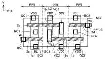
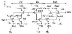
図1は、この発明の実施の形態1に従う半導体記憶装置のメモリセルのレイアウトを概略的に示す図である。図1においては、トランジスタが形成される活性領域、ポリシリコン層およびコンタクトのレイアウトを概略的に示す。図1に示すメモリセルMCは、シングルポートメモリセルであり、1ビットの情報を記憶する。[Embodiment 1]
FIG. 1 schematically shows a layout of memory cells of a semiconductor memory device according to the first embodiment of the present invention. FIG. 1 schematically shows the layout of an active region where a transistor is formed, a polysilicon layer, and contacts. The memory cell MC shown in FIG. 1 is a single-port memory cell and stores 1-bit information.
図1において、n型の半導体基板領域(Nウェル)NWがY方向に直線的に延在して配置され、NウェルNWの両側に、p型基板領域(Pウェル)PW1およびPW2が配置される。NウェルNWに、負荷トランジスタが形成され、PウェルPW1およびPW2に、それぞれ、アクセストランジスタおよびドライバトランジスタが配置される。これらのウェルNW、PW1およびPW2は、列方向に連続的に延在して配置され、これらのウェルNW、PW1およびPW2において、1列に整列するメモリセルが形成される。 In FIG. 1, n-type semiconductor substrate regions (N wells) NW are arranged extending linearly in the Y direction, and p-type substrate regions (P wells) PW1 and PW2 are arranged on both sides of the N well NW. The A load transistor is formed in N well NW, and an access transistor and a driver transistor are arranged in P wells PW1 and PW2, respectively. These wells NW, PW1 and PW2 are arranged extending continuously in the column direction, and in these wells NW, PW1 and PW2, memory cells aligned in one column are formed.
PウェルPW1において、Y方向に延在する矩形形状の活性領域1aが形成される。活性領域1aと交差するようにX方向にワード線を構成するポリシリコン配線2aおよび2bが配設される。ポリシリコン配線2aは、PウェルPW1において配置され(隣接列のメモリセル領域内にまで延在する)、ポリシリコン配線2bは、NウェルNW内にまで延在する。 In the P well PW1, a rectangular
ポリシリコン配線2aおよび2bの間に、ストレージノードを形成するためのコンタクトNC1が配設される。ポリシリコン配線2aの外側の活性領域1aの領域において、ビット線BLに対するコンタクトをとるためのビット線コンタクトBC1が配設され、活性領域1aの対向する端部において活性領域1aに対し、ロー側電源(ソース)線(VSSソース線)に対するコンタクトをとるためのソースコンタクトGC1が形成される。 A contact NC1 for forming a storage node is arranged between
NウェルNWにおいては、Y方向に延在する矩形形状の活性領域1bおよび1cが間をおいてかつY方向において位置をずらせて形成される。活性領域1bを横切るように、ポリシリコン配線2bがX方向に延在して配設される。活性領域1cに対しても、X方向に延在するポリシリコン配線2cが配設される。活性領域1bは、一方端部領域において、ハイ側電源線(VDDソース線)に対するコンタクトをとるための電源コンタクトVC1が形成される。活性領域1bのポリシリコン配線2bに関して対向する端部においては、ポリシリコン配線2cに対して共通にコンタクトをとる共有コンタクト(シェアードコンタクト)SC1が形成される。共有コンタクトSC1を利用することにより、1つのコンタクトにより、活性領域1bおよびポリシリコン配線2c両者に対する電気的接続がとられる。 In N well NW, rectangular
同様、活性領域1cにおいても、ポリシリコン配線2cの外部に、VDDソース線に対するコンタクトをとるための電源コンタクトVC2が形成され、活性領域1cのポリシリコン配線2cに対向する領域において、共有コンタクトSC2が設けられ、活性領域1cおよびポリシリコン配線2bが電気的に接続される。 Similarly, in the
PウェルPW2において、PウェルPW1と同様、Y方向に延在する矩形形状の活性領域1dが設けられる。活性領域1dに対しては、活性領域1aと対称な位置に、VSSソース線に対するソースコンタクトGC2およびビット線/BLに対するビット線コンタクトBC2が形成される。また、ストレージノードを形成するためのコンタクトNC2が、活性領域1dのY方向についての中央領域に形成される(1つのメモリセル内において)。コンタクトBC2およびNC2の間に、X方向に延在するポリシリコン配線2dが形成される。このポリシリコン配線2dは、PウェルPW2内において延在する(隣接列にまで延在するが、隣接列のメモリセルは示していない)。コンタクトNC2およびGC2の間に、ポリシリコン配線2cが、Nウェルの共有コンタクトSC1から連続的にX方向に延在して配設される。 In the P well PW2, as in the P well PW1, a rectangular
ポリシリコン配線2dに対しては、ワード線WLに対するコンタクトをとるためのコンタクトWC2が形成される。 A contact WC2 for making contact with the word line WL is formed for the
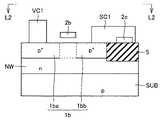
図2は、図1に破線L2−L2で示される活性領域1bのY方向に沿った断面構造を概略的に示す図である。図2において、p型半導体基板SUB上にNウェルNWが形成され、このNウェルNWの表面に、活性領域1bが形成される。活性領域1bには、その一端部において素子分離膜(フィールド絶縁膜)5が形成され、他のトランジスタ活性領域と分離される。活性領域1bにおいては、高濃度の不純物領域1baおよび1bbが間をおいて形成される。これらの不純物領域1baおよび1bbの間のNウェルNWの表面上に、ポリシリコン配線2bが配設される。不純物領域1baが、電源コンタクトVC1に電気的に接続される。この不純物領域1baは、Y方向において隣接するメモリセルと共有され、この不純物領域1baに対しては素子分離膜は形成されない。 FIG. 2 is a diagram schematically showing a cross-sectional structure along the Y direction of
コバルトシリサイドCoSiまたはニッケルシリサイドNiSiなどのシリサイド膜が、通常、コンタクトVC1と不純物領域1baの間にバリア層として形成されるが、図2においては、このシリサイド膜は示していない。不純物領域1bbについても同様である。 A silicide film such as cobalt silicide CoSi or nickel silicide NiSi is usually formed as a barrier layer between the contact VC1 and the impurity region 1ba, but this silicide film is not shown in FIG. The same applies to impurity region 1bb.
素子分離膜5上に、ポリシリコン配線2cが配設される。このポリシリコン配線2cに対して、不純物領域1bbと電気的に接続する共有コンタクトSC1が電気的に接続される。したがって、共有コンタクトSC1を介して、不純物領域1bbおよびポリシリコン配線2cが電気的に接続される。不純物領域1bbとポリシリコン配線2cを電気的に接続するための別の配線層の配線が不要となり、配線レイアウトが簡略化され、また、上層の配線層において、余裕を持って配線レイアウトを行うことができる。また、共有コンタクトSC1およびSC2を用いることにより、他のコンタクトと同一製造工程で、各コンタクトを形成することができる(共有コンタクトSC1およびSC2のみが、他のコンタクトとその平面形状が異なる)。 A
なお、ポリシリコン配線2b下部のNウェルNWの表面領域には、MOSトランジスタのしきい値電圧調整のためのカウンタドープ等により不純物注入が行なわれてもよい。 Impurity implantation may be performed in the surface region of N well NW below
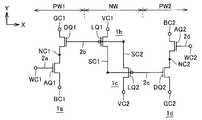
図3は、図1に示すメモリセルにおけるトランジスタの配置を示す電気的等価回路図である。図3において、PウェルPW1において、活性領域1a内にドライバトランジスタDQ1およびアクセストランジスタAQ1が形成される。ドライバトランジスタDQ1は、そのソースノードがコンタクトGC1に接続され、そのドレインノードがコンタクトNC1に接続され、そのゲートがポリシリコン配線2bにより形成される。アクセストランジスタAQ1は、コンタクトNC1とビット線コンタクトBC1の間に配置されかつそのゲートが、コンタクトWC1に接続されるポリシリコン配線2aにより形成される。 FIG. 3 is an electrical equivalent circuit diagram showing the arrangement of transistors in the memory cell shown in FIG. In FIG. 3, in P well PW1, driver transistor DQ1 and access transistor AQ1 are formed in
NウェルNWにおいては、活性領域1b内に、pチャネルMOSトランジスタで構成される負荷トランジスタLQ1が形成され、活性領域1c内には、pチャネルMOSトランジスタで構成される負荷トランジスタLQ2が形成される。負荷トランジスタLQ1は、ソースノードが電源コンタクトVC1に接続され、かつドレインノードが共有コンタクトSC1を介してポリシリコン配線2cに接続される。負荷トランジスタLQ1のゲートは、ポリシリコン配線2bにより形成される。ポリシリコン配線2bが、共有コンタクトSC2を介して、負荷トランジスタLQ2のドレインノードに接続される。負荷トランジスタLQ2のソースノードは、電源コンタクトVC2に接続され、そのゲートがポリシリコン配線2dにより形成される。 In N well NW, a load transistor LQ1 composed of a p-channel MOS transistor is formed in
PウェルPW2において、活性領域1d内に、それぞれ、NチャネルMOSトランジスタで構成されるアクセストランジスタAQ2およびドライバトランジスタDQ2が形成される。アクセストランジスタAQ2は、そのゲートがポリシリコン配線2dにより形成され、このポリシリコン配線2dが、コンタクトWC2に接続される。アクセストランジスタAQ2は、その両導通ノードがそれぞれコンタクトBC2およびコンタクトNC2に接続される。ドライバトランジスタDQ2が、コンタクトGC2とコンタクトNC2の間に配置され、かつそのゲートがポリシリコン配線2cにより形成される。 In P well PW2, access transistor AQ2 and driver transistor DQ2 each formed of an N channel MOS transistor are formed in
したがって、PウェルPW1およびPW2各々において、2つのNチャネルMOSトランジスタが整列して活性領域1aおよび1d内に形成される。NウェルNWにおいて、負荷トランジスタLQ1およびLQ2をそれぞれ別々に設けられた活性領域1bおよび1c内に形成する。したがって、Y方向におけるメモリセルのピッチは、トランジスタ2個に相当するピッチであり、Y方向におけるメモリセルサイズが増大するのを抑制する。 Therefore, in each of P wells PW1 and PW2, two N channel MOS transistors are aligned and formed in
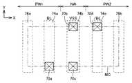
図4は、図1のメモリセルMCのレイアウトに対するコンタクトおよび上層の第1金属配線のレイアウトを概略的に示す図である。図4において、図1に示すコンタクトと同じコンタクトには同一参照番号を付し、その詳細説明は省略する。 FIG. 4 is a diagram schematically showing a layout of contacts and upper first metal wirings with respect to the layout of memory cell MC of FIG. 4, the same contacts as those shown in FIG. 1 are denoted by the same reference numerals, and detailed description thereof is omitted.
コンタクトWC1に対し、第1金属配線7aがY方向に延在する矩形形状に形成される。この第1金属配線7aに対しては、ビアWV1が形成される。コンタクトGC1に対しては、第1金属配線7bが配置される。この第1金属配線7bに対しては、コンタクトGC1とほぼ重なり合うようにビアGV1が形成される。コンタクトNC1に対しては、共有コンタクトSC1にまでX方向に延在する矩形形状の第1金属配線7dが形成される。 With respect to contact WC1,
コンタクトBC1に対して第1金属配線7cが設けられる。このコンタクトBC1と平面的に一部が重なり合うように、ビアBV1が第1金属配線7cに対して形成される。
電源コンタクトVC1に対して、第1金属配線7eが設けられる。この第1金属配線7eに対しては、コンタクトVC1と一部が重なり合うようにビアVV1が形成される。 A
コンタクトVC2に対して第1金属配線7fが、形成される。第1金属配線7fに対しては、コンタクトVC2と重なり合うようにビアVV2が形成される。共有コンタクトSC2およびコンタクトNC2に対しては、第1金属配線7gがX方向に延在する矩形形状に形成される。 First metal interconnection 7f is formed for contact VC2. A via VV2 is formed for first metal interconnection 7f so as to overlap with contact VC2. For shared contact SC2 and contact NC2,
コンタクトBC2に対して第1金属配線7hが形成され、この第1金属配線7h上部に、コンタクトBC2と一部が重なり合うようにビアBV2が形成される。 A
コンタクトGC2に対して第1金属配線7iが形成され、また、個の第1金属配線7iに対してコンタクトGC2と重なり合うようにビアGV2が形成される。
コンタクトWC2に対しては、Y方向に長辺を有する矩形形状に第1金属配線7jが形成される。この第1金属配線7jに対しては、ビアWV2が設けられる。これらのビアWV1、WV2、BV1、BV2、GV1、GV2、VV1、およびVV2は、これらの第1金属配線上にさらに形成される第2金属配線との電気的コンタクトをとるために設けられる。 For contact WC2,
図4に示す第1金属配線7a−7jは、メモリセル内部においてのみ延在し、内部のストレージノードの電気的接続を取るまたは上層配線との接続をとるための中間配線として利用される。
すなわち、第1金属配線7a−7jにより、図3に示す電気的等価回路において、ノードNC1が、共有ノードSC1に結合されて、負荷トランジスタLQ2およびドライバトランジスタDQ2のゲートが共通に内部ノード(ストレージノード;コンタクトNC1)に接続され、また、コンタクトNC2が、共有コンタクトSC2に接続されて、他方のストレージノードが、ドライバトランジスタDQ1および負荷トランジスタLQ1のゲートに接続される。 That is, in the electrical equivalent circuit shown in FIG. 3, node NC1 is coupled to shared node SC1 by
第1金属配線7bおよび7iは、それぞれ、VSSソース線(ロー側電源線)に接続されるが、X方向に隣接するメモリセルとは非共有とされる。メモリセルは、メモリセルの境界線(X方向およびY方向両方向において)について鏡映対称に配置される。しかしながら、この第1金属配線7bおよび7iは、隣接メモリセルの対応の第1金属配線とは隙間が設けられており、鏡映対称配置時において、隣接列のメモリセルの対応の第1金属配線とは分離される。 The
図5は、図4に示すメモリセルの配線レイアウトに対する上層の配線レイアウトを概略的に示す図である。図5においては、第2金属配線および対応のビアの配置を示し、また、図4に示すコンタクトと同一のコンタクトに対しては同一参照番号を付し、その詳細説明は省略する。 FIG. 5 schematically shows an upper layer wiring layout relative to the memory cell wiring layout shown in FIG. In FIG. 5, the arrangement of the second metal wiring and the corresponding via is shown, and the same reference number is assigned to the same contact as the contact shown in FIG. 4, and the detailed description thereof is omitted.
図5において、コンタクトWV1に対し、メモリセル領域内においてY方向に延在する矩形形状の第2金属配線9aが配設される。この第2金属配線9aに対して、第2のビアWWV1がビアWV1と一部が重なり合うように形成される。ビアBV1に対し、第2金属配線9cが設けられる。第2金属配線9cに対しては、ビアBV1と重なり合うように第2ビアBBV2が設けられる。ビアVV1に対して、第2金属配線9dが設けられる。またビアVV2に対し、第2金属配線9eが設けられる。第2金属配線9dおよび9eに対し、Y方向に整列する位置に、それぞれ、第2ビアVVV1およびVVV2が設けられる。 In FIG. 5, a rectangular
ビアBV2に対し第2金属配線9fが設けられ、この第2金属配線9f上部に、第2ビアBBV2が設けられる。 A
ビアWV2に対して第2金属配線9gが設けられる。この第2金属配線9gに対し、X方向において第2金属配線9aに対する第2ビアWWV1と整列するように第2ビアWWV2が設けられる。
ビアGV1およびGV2の間に、第2金属配線9bが階段状に連続的に延在するように形成される。この第2金属配線9bは、X方向およびY方向に直線的に延在する部分を有し、中心部に関して点対称なL字形状を有し、その両端でビアGV1およびGV2に接続される。 Between vias GV1 and GV2,
したがって、メモリセルMCにおいて、2つのドライバトランジスタのVSSソース線に接続されるノードが、第2金属配線9bにより短絡される。メモリセルMC内のNウェル(図5には示さず)をX方向に横切るように延在し、第2金属配線9bは、メモリセル内においてのみドライバトランジスタのソースノードを短絡する。すなわち、第2金属配線9bは、直線的にY方向およびX方向に延在し、最短距離でドライバトランジスタのソースノードに対応するビアGV1およびGV2を電気的に接続する。第2金属配線9bは、メモリセルMC内においてのみ延在し、X方向に隣接するメモリセル内の対応の第2金属配線9bとは、互いに分離される。 Accordingly, in the memory cell MC, the node connected to the VSS source line of the two driver transistors is short-circuited by the
図6は、図5に示すレイアウト完了時のメモリセルにおけるトランジスタの接続を示す電気的等価回路図である。図6において、図4に示す第1金属配線7dにより、内部ノードNC1が共有ノードSC1に接続され、第1金属配線7gにより、内部ノードNC2が共有ノードSC2に接続される。第1金属配線7dにより、トランジスタLQ2およびドライバトランジスタDQ2のゲートがストレージノードに対応するコンタクトNC1に接続されて、また、負荷トランジスタLQ1およびドライバトランジスタDQ1のゲートが、別のストレージノードに対応するコンタクトNC2に接続される。 FIG. 6 is an electrical equivalent circuit diagram showing transistor connections in the memory cell when the layout shown in FIG. 5 is completed. In FIG. 6, internal node NC1 is connected to shared node SC1 by
ドライバトランジスタDQ1のソースノードは、ビアGV1および第2金属配線9bを介して、ドライバトランジスタDQ2のVSSソースノードのビアGV2に接続される。第2金属配線9bは、第1金属配線7dおよび7gよりも上層の配線であり、図5に示すように、これらの金属配線9b、7dおよび7gが平面図的に見て互いに重なり合うように配置される。 The source node of driver transistor DQ1 is connected to via GV2 of the VSS source node of driver transistor DQ2 via via GV1 and
なお、アクセストランジスタAQ1およびAQ2各々のゲートノードおよび一方導通ノードおよび負荷トランジスタLQ1およびLQ2のソースノードは、それぞれ、ビアにより接続されるものの、図5に示すように、これらのビアは、上層配線に対する接続をとるためのビアで構成され、図6においては、これらのノードの接続先はまだ形成されていないため、特に明確には示していない。 Although the gate nodes and one conduction node of each of access transistors AQ1 and AQ2 and the source nodes of load transistors LQ1 and LQ2 are connected by vias, respectively, as shown in FIG. In FIG. 6, the connection destinations of these nodes are not yet clearly shown because they are not formed yet.
図6に示すように、メモリセル内において、NウェルNWをX方向に横切るように、第2金属配線9bを、階段状の直線形状に形成することにより、最短距離でドライバトランジスタDQ1およびDQ2のソースノードを短絡でき、メモリセル内においてドライバトランジスタのVSSソースノードに電位差が生じるのを抑制することができる。 As shown in FIG. 6, in the memory cell, the
図7は、図5に示す配線レイアウトのさらに上層に配置されるの第3および第4金属配線のレイアウトを概略的に示す図である。図7において、ビアWWV1に対し、メモリセルMC内においてY方向に延在する矩形形状の第3金属配線10aが設けられる。第2ビアBBV1に対し、Y方向に連続的に延在する第3金属配線10bが設けられ、この第3金属配線10bにより、ビット線BLが実現される。 FIG. 7 schematically shows a layout of third and fourth metal wirings arranged in a further upper layer of the wiring layout shown in FIG. In FIG. 7, a rectangular
ビアVVV1およびVVV2に対し、第3金属配線10cが設けられる。この第3金属配線10cはY方向に連続的に延在し、対応の列に配設されるメモリセルに対してハイ側ソース電圧(電源電圧)VDDを供給する。
ビット線ビアBBV2に対し、Y方向に連続的に延在する第3金属配線10dが設けられ、この第3金属配線10dによりビット線/BLが実現される。ビアWWV2に対し、メモリセルMC内においてY方向に延在する矩形形状の第3金属配線10eが設けられる。第3金属配線10aおよび10eに対し、X方向に連続的に延在する第4金属配線11が設けられる。第4金属配線11は、ビアWWV1およびWWV2それぞれと重なり合うように形成されるビアVA1およびVA2を介してそれぞれ、第3金属配線10aおよび10eに接続される。この第4の金属配線11によりX方向に整列するメモリセルに対するワード線WLが実現され、X方向に整列するメモリセル各々のアクセストランジスタAQ1およびAQ2のゲートが共通に接続される。 A
図7に示すように、第3金属配線は、ロー側電源電圧(ソース電圧)VSSを伝達する配線としては用いられていない。メモリセルのドライバトランジスタの(VSS)ソースノードは、第2金属配線により相互接続される。メモリセルMC上において、ロー側電源電圧VSSを伝達するための第3金属配線は不要となり、この第3金属配線層において、配線レイアウトピッチに余裕をもって必要な配線を配置することができる。 As shown in FIG. 7, the third metal wiring is not used as a wiring for transmitting the low-side power supply voltage (source voltage) VSS. The (VSS) source nodes of the driver transistors of the memory cells are interconnected by a second metal wiring. On the memory cell MC, the third metal wiring for transmitting the low-side power supply voltage VSS is not necessary, and the necessary wiring can be arranged in the third metal wiring layer with a margin in the wiring layout pitch.
図8は、図7の線L8−L8に沿った断面構造を概略的に示す図である。図8において、p型半導体基板SUB表面にNウェルNWが形成される。NウェルNW表面に互いに分離してp型不純物領域1baおよび1bbが形成される。これらの不純物領域1baおよび1bbが、図1に示す活性領域1bに含まれる。不純物領域1bbに隣接して素子分離膜5がNウェルNWの表面に形成される。また、不純物領域1baおよび1bbの間のNウェルNW表面上にゲート絶縁膜を介してポリシリコン配線2bが形成される。 FIG. 8 schematically shows a cross-sectional structure taken along line L8-L8 in FIG. In FIG. 8, an N well NW is formed on the surface of a p-type semiconductor substrate SUB. P-type impurity regions 1ba and 1bb are formed separately on the surface of N well NW. These impurity regions 1ba and 1bb are included in
素子分離膜5上にポリシリコン配線2cが形成され、このポリシリコン配線2cは、共有コンタクトSC1を介して不純物領域2cに接続される。不純物領域1baは、コンタクトVC1に結合される。このコンタクトVC1および共有コンタクトSC1までの構造は図2に示す構造と同じである。
なお、共有コンタクトSC1、ポリシリコン配線2bおよびコンタクトVC1は、層間絶縁膜12aにより互いに電気的に分離される。 Shared contact SC1,
コンタクトVC1に接続するように第1金属配線7eが形成され、また、共有コンタクトSC1と接続するように第1金属配線7dが形成される。これらの第1金属配線7eおよび7dは、層間絶縁膜12bにより互いに電気的に分離される。この層間絶縁膜12bにフォトリソグラフィ工程(写真製版およびエッチング工程)により第1金属配線7eに達するビアホールが形成され、次いで、このビアホールを導電材で充填することにより、第1金属配線7eと電気的に接続される第1ビアVV1が形成される。
層間絶縁膜12b上に第1金属配線7eおよび7dと整列するように第2金属配線9dおよび9bが形成される。第2金属配線9bおよび9dは層間絶縁膜12cにより互いに電気的に分離される。
層間絶縁膜12c上に第3金属配線10cが配置され、層間絶縁膜12cに形成された第2ビアVVV1により第2金属配線9dおよび第3金属配線10dが電気的に接続され、下層の不純物領域1baにハイ側電源電圧VCCが供給される。この第3金属配線10c上層に第3金属配線と交差する方向に第4金属配線11が配置される。
この図8に見られるように、メモリセルのソースノードを相互接続するVSSソース線は、第2金属配線9bで構成されており、メモリセルの内部配線およびワード線のレイアウトに悪影響を及ぼすことなく、メモリセルソースノード接続配線をメモリセル内に配置することができる。 As shown in FIG. 8, the VSS source line interconnecting the source nodes of the memory cells is formed of the
図9は図7に示す線L9−L9に沿った断面構造を概略的に示す図である。図9において、p型半導体基板SUB表面にPウェルPW1およびPW2が形成され、これらの間にNウェルNWが配置される。PウェルPW1の表面にn型活性領域(不純物領域)1aが形成され、NウェルNW表面に互いに間を置いてp型活性領域1bおよび1cが形成される。PウェルPW2の表面にn型活性領域1dが形成される。これらの活性領域1a−1dは、素子分離膜(領域)5により互いに分離される。 FIG. 9 schematically shows a cross-sectional structure along line L9-L9 shown in FIG. In FIG. 9, P wells PW1 and PW2 are formed on the surface of a p-type semiconductor substrate SUB, and an N well NW is disposed therebetween. An n-type active region (impurity region) 1a is formed on the surface of P well PW1, and p-type
図示しない層間絶縁膜の形成後、第1金属配線7a、7d、7gおよび7jが形成される。第1金属配線7dは、コンタクトNC1および共有コンタクトSC1をそれぞれ介して活性領域1aおよび1Bに電気的に接続される。第1金属配線7gは、共有コンタクトSC2およびコンタクトNC2をそれぞれ介して活性領域1cおよび1dに電気的に接続される。第1金属配線7aおよび7jは、図示しない部分においてポリシリコン配線に接続される。 After the formation of an interlayer insulating film (not shown),
第1金属配線7aおよび7jと整列して第2金属配線9aおよび9gが配置され、第1金属配線7dおよび7g上層にこれらと平面図的に見て重なり合うように第2金属配線9bが配置される。第2金属配線9aは第1ビアWV1を介して第1金属配線7aに電気的に接続され、第2金属配線9gは、第1ビアWV2を介して第1金属配線7jに電気的に接続される。第2金属配線9bは、メモリセルのVSSソースノードを接続する配線であり、下層の第1金属配線7dおよび7gとは電気的に分離される。
第2金属配線9b上層に互いに間を置いて第3金属配線10b、10cおよび10eが配置される。第3金属配線10bおよび10eが、それぞれビット線BLおよび/BLの一部を構成し、第3金属配線10cは、ハイ側電源電圧VDDを供給する。
これらの第3金属配線10b、10cおよび10eの上層に連続的に延在して第4金属配線11が配置される。この第4金属配線11は、ワード線WLの一部を構成し、第2ビアWWV1およびWWV2をそれぞれ介して第2金属配線9aおよび9gに電気的に接続される。 A
この図9に示すように、ワード線延在方向においても、ロー側電源電圧VSSを伝達する配線9bは、内部ノード(ストレージノード)接続用の第1金属配線7dおよび7gと平面図的に見て重なり合うように配置されており、何らメモリセルのサイズを増大させることなく、メモリセルロー側ソースノードを電気的に接続する配線を配置することができる。 As shown in FIG. 9, even in the word line extending direction,
図10は、4行2列に配列されるメモリセルの第2金属配線配設時の配線レイアウトを概略的に示す図である。図10において、X方向に隣接するメモリセルMCの境界領域には、ワード線を構成する第4金属配線へのコンタクトをとるための第2金属配線9gがY方向およびX方向において整列して配置される。X方向において隣接する列のメモリセルは、PウェルPWを共有し、一方、NウェルNWは、Y方向に整列するメモリセルにおいてのみ共有される。 FIG. 10 schematically shows a wiring layout when the second metal wiring of the memory cells arranged in 4 rows and 2 columns is provided. In FIG. 10, in the boundary region of memory cells MC adjacent in the X direction,
メモリセルにおいて、VSSソースノードを構成するビアGV1およびGV2が、第2金属配線9bにより相互接続される。Y方向に隣接するメモリセルMCにおいては、境界領域に関して鏡映対称なレイアウトが繰返し配置されており、VSSソース線は、各メモリセル列ごとに、ジグザグ形状に配列されて、各列(Y方向に整列するメモリセル)ごとに、このロー側電源電圧VSSの電圧レベルを調整することができる。すなわち、X方向において隣接するメモリセルMCにおいては、ビアGV2が分離して配置されており、隣接列における第2金属配線9bは互いに分離されており、したがって、メモリセル列ごとに、ロー側電源電圧VSSを調整することができる。また、メモリセルMC内においては、それぞれドライバトランジスタのソースノードが短絡されており、ビット線放電時においてもドライバトランジスタのソースノードの電位差を抑制でき、メモリセルを安定に動作させることができる。 In the memory cell, vias GV1 and GV2 constituting a VSS source node are interconnected by a
また、メモリセル列単位で、電圧VSSの調整が可能であり、先の非特許文献1および2に示されるVSSソース線電圧をダイナミックに制御する方式を利用することができ、選択列に対しては電圧VSSを接地電圧レベルに設定し、非選択列に対しては電圧VSSを接地電圧より高い電圧レベル(たとえば0.4V)に設定することにより、スタンバイ時および動作時の消費電流を低減することができる。 Further, the voltage VSS can be adjusted in units of memory cell columns, and the method of dynamically controlling the VSS source line voltage shown in the previous Non-Patent Documents 1 and 2 can be used. Sets the voltage VSS to the ground voltage level and sets the voltage VSS to a voltage level higher than the ground voltage (for example, 0.4 V) for the non-selected columns, thereby reducing current consumption during standby and operation. be able to.
ドライバトランジスタのソース電圧VSSを、メモリセル列ごとに調整する構成としては、前述の非特許文献1および2に示される構成を利用することができる。すなわち、コラムアドレス信号に基づいて選択列に対するドライバトランジスタのソース電圧VSSの電圧レベルを設定する。その場合、電圧切換タイミングを与える信号としては、SRAMにおいて通常用いられるアドレス変化検出信号(ATD)またはアクセスサイクルを規定するクロック信号が用いられればよい。 As a configuration for adjusting the source voltage VSS of the driver transistor for each memory cell column, the configurations described in Non-Patent Documents 1 and 2 described above can be used. That is, the voltage level of the source voltage VSS of the driver transistor for the selected column is set based on the column address signal. In this case, an address change detection signal (ATD) usually used in SRAM or a clock signal defining an access cycle may be used as a signal for giving voltage switching timing.
また、VSSソース線9bがメモリセル列方向(Y方向)に沿ってジグザグ状に配置されるため、列方向に直線的に延在するレイアウトに比べて配線長が長くなり、配線抵抗の増大によりVSSソース線9bにおいてメモリセルソース電圧VSSの浮き上がり(分布)が大きくなる可能性が考えられる。しかしながら、VSSソース配線9bは、各列において個々に配設されており、ワード線選択時には、選択ワード線に接続される1つのメモリセルからの放電電流が流れ込むだけであり、電流量は小さく、ソース電位の浮き上がりは十分に小さく、また、メモリセルのドライバトランジスタのソースノードが相互接続されており、各メモリセルにおいては、ドライバトランジスタのソースノードの電位はほぼ等しいため、非選択メモリセルにおいては安定にデータを保持することができ、また、選択メモリセルにおいてもデータ読出時においては安定にデータを保持することができる。 Further, since the
また、VSSソース配線は金属配線であり、その抵抗値は十分に小さく、配線抵抗による電位分布の問題はほぼ抑制することができる。すなわち、第2金属配線のシート抵抗は、約200mΩ/□であり、VSSソース配線の1ビットのメモリセルあたりの配線長を屈曲(ジグザグ形状)を考慮して約1μm、配線幅を0.1μm、全行数を512とすると、VSSソース配線全体の配線抵抗Rallは、200mΩ・L/Wから、次式で示される。 Further, the VSS source wiring is a metal wiring, and its resistance value is sufficiently small, and the problem of potential distribution due to wiring resistance can be substantially suppressed. That is, the sheet resistance of the second metal wiring is about 200 mΩ / □, the wiring length per 1-bit memory cell of the VSS source wiring is about 1 μm considering the bending (zigzag shape), and the wiring width is 0.1 μm. When the total number of rows is 512, the wiring resistance Rall of the entire VSS source wiring is expressed by the following equation from 200 mΩ · L / W.
Rall=200m・1μm・512/0.1μm≒1KΩ
ハイ側電源電圧VDDが1.0Vで、セル電流が10μAとすると、ロー側電源ノードから最も遠いメモリセルにおいてロー側電源電圧VSSの上昇は、10μA・1KΩ=0.01Vであり、ハイ側電源電圧VDDの1.0Vに比べて十分に小さい。また、メモリセル内においては、配線抵抗は1Ω(=200mΩ・1μm/0.1μm)であり、ドライバトランジスタのソースノードの電圧差は、1.0μV(=1Ω・10μA)であり、電圧保持特性に対する影響はほぼ無視することができる。Rall = 200m ・ 1μm ・ 512 / 0.1μm ≒ 1KΩ
When the high-side power supply voltage VDD is 1.0 V and the cell current is 10 μA, the rise of the low-side power supply voltage VSS is 10 μA · 1 KΩ = 0.01 V in the memory cell farthest from the low-side power supply node. It is sufficiently smaller than the voltage VDD of 1.0V. In the memory cell, the wiring resistance is 1Ω (= 200 mΩ · 1 μm / 0.1 μm), the voltage difference of the source node of the driver transistor is 1.0 μV (= 1Ω · 10 μA), and voltage holding characteristics The effect on is almost negligible.
以上のように、この発明の実施の形態1に従えば、メモリセルのドライバトランジスタのソースノードを、階段状にメモリセル内において延在しかつメモリセル列方向においてジグザグ状に延在する第2金属配線(ビット線より下層の金属配線)を用いて相互接続し、隣接列間でのVSSソース線は互いに分離されており、各メモリセル列ごとにメモリセルのロー側電源電圧VSSの設定を行なうことができる。 As described above, according to the first embodiment of the present invention, the source node of the driver transistor of the memory cell extends in the stepwise manner in the memory cell and extends in the zigzag manner in the memory cell column direction. Interconnection is performed using metal wiring (metal wiring below the bit line), and VSS source lines between adjacent columns are separated from each other, and the low-side power supply voltage VSS of the memory cell is set for each memory cell column. Can be done.
また、メモリセルMCにおいては、Nウェルの両側にPウェルを設け、各Pウェルにアクセストランジスタおよびドライバトランジスタを配置し、Nウェルに負荷トランジスタを配置しており、Y方向におけるメモリセルのピッチはトランジスタ2個のピッチであり、メモリセルのサイズがY方向において増大するのを抑制することができる。 In the memory cell MC, P wells are provided on both sides of the N well, an access transistor and a driver transistor are arranged in each P well, and a load transistor is arranged in the N well. The pitch of the memory cells in the Y direction is The pitch of two transistors can suppress an increase in the size of the memory cell in the Y direction.
また、ハイ側電源電圧VDDを伝達する電源線とロー側電源電圧VSSを伝達する電源線とは、別の配線層の配線で形成しており、電源電圧VDDおよびVSSが同一の配線層の配線で伝達されないため、上層の配線層の配線ピッチ条件を緩和することができる。 Further, the power supply line for transmitting the high-side power supply voltage VDD and the power supply line for transmitting the low-side power supply voltage VSS are formed by wirings of different wiring layers, and the wirings of the wiring layers having the same power supply voltage VDD and VSS are formed. Therefore, the wiring pitch condition of the upper wiring layer can be relaxed.
[実施の形態2]
図11は、この発明の実施の形態2に従う半導体記憶装置のメモリセルのレイアウトを概略的に示す図である。図9においては、デュアルポートSRAMセルDPMCの活性領域および第1ポリシリコン配線のレイアウトが示される。[Embodiment 2]
FIG. 11 schematically shows a layout of the memory cell of the semiconductor memory device according to the second embodiment of the present invention. FIG. 9 shows the layout of the active region of the dual port SRAM cell DPMC and the first polysilicon wiring.
図11において、デュアルポートSRAMセルDPMCは、NウェルNWと、このNウェルNW両側に配置されるPウェルPW1およびPW2の領域に形成される。PウェルPW1においては、活性領域15aがメモリセル形成領域内においてY方向に延在して矩形形状に配置され、活性領域15bが活性領域と分離されてY方向に延在して形成される。活性領域15aはY方向において隣接するメモリセルにおいて延在し、活性領域15bは、Y方向に整列する一列のメモリセルに対して連続的に延在して配置される。 In FIG. 11, dual port SRAM cell DPMC is formed in regions of N well NW and P wells PW1 and PW2 arranged on both sides of N well NW. In P well PW1,
活性領域15aおよび15bを横切るようにX方向に延在して、第1ポリシリコン配線16aおよび16bが、それぞれ間をおいて形成される。第1ポリシリコン配線16aは、図示しない隣接メモリセルのPウェル領域まで延在し、一方、第1ポリシリコン配線16bは、PウェルPW1からNウェルNWまで延在する。
第1ポリシリコン配線16aには、ソース線コンタクト17aが設けられる。活性領域15aにおいては、その一方端部においてコンタクト17bが形成され、その他方端領域において、共有コンタクト18aが設けられる。この共有コンタクト18aにより、第1ポリシリコン配線16bと活性領域15aが電気的に接続される。 A
活性領域15bに対しても、第1ポリシリコン配線16aを間に挟むようにコンタクト17cおよび17dが設けられ、また、第1ポリシリコン配線16bに関してコンタクト17dと対向するようにコンタクト17cが設けられる。コンタクト17cは、VSSソース線に接続するためのコンタクトである。一方、活性領域15aおよび15b二形成されるコンタクト17bおよび17eは、Aポートビット線およびBLAおよび/BLAにそれぞれ接続するためのコンタクトである。 Also for
NウェルNWにおいて、活性領域15cおよび15dが、互いに間をおいてかつY方向において位置をずらせて、Y方向に延在する矩形形状に形成される。活性領域15cを横切るように、第1ポリシリコン配線16bがX方向に延在し、また活性領域15dを横切るようにX方向に延在して第1ポリシリコン配線16cが配設される。第1ポリシリコン配線16bは、活性領域15dと共有コンタクト18cにより電気的に接続され、第1ポリシリコン配線16cが、また、共有コンタクト18bを介して活性領域15cに接続される。 In N well NW,
活性領域15cの第1ポリシリコン配線16bに関して共有コンタクト18bと対向する端部においてコンタクト17fが形成され、また、活性領域15dにおいても、共有コンタクト18cと対向する端部においてコンタクト17jが形成される。コンタクト17fおよび17gは、それぞれ、ハイ側電源電圧VDDを伝達するVDDソース線に接続するためのコンタクトである。 A
PウェルPW2において、また、Y方向に延在して、それぞれ互いに分離して活性領域15eおよび15fが形成される。第1ポリシリコン配線16cが、活性領域15eを横切るようにNウェルNWからX方向に連続的に延在して配設される。また、活性領域15eおよび15fを横切るようにX方向に延在して第1ポリシリコン配線16dが形成される。活性領域15eにおいては、その対向端部にコンタクト17hおよび17jがそれぞれ形成され、その中央領域において、コンタクト17iが形成される。コンタクト17hは、Bポートビット線BLBに接続するためのコンタクトであり、コンタクト17gは、VSSソース線に接続するためのコンタクトである。活性領域15fは、共有コンタクト18dにより第1ポリシリコン配線16cにその一方側領域が接続され、他方側領域にコンタクト17kが形成される。コンタクト17kは、Bポートビット線/BLBに接続するためのコンタクトである。 In P well PW2,
第1ポリシリコン配線16dには、メモリセル境界領域においてBポートワード線WLBに接続するためのコンタクト17lが形成される。コンタクト17lは、図示しないX方向において隣接するメモリセルと共有される(第1ポリシリコン配線16dが、隣接列のメモリセルのPウェル領域まで延在する)。 A contact 17l for connecting to the B port word line WLB is formed in the
この図11に示す配線レイアウトにおいても、X方向およびY方向において鏡映対称にメモリセルの活性領域および配線が配置される。したがって、活性領域15bおよび15eがY方向に連続的に延在して配置される。 Also in the wiring layout shown in FIG. 11, the active regions and wirings of the memory cells are arranged in mirror symmetry in the X direction and the Y direction. Therefore,
図12は、図11に示す配線レイアウトのメモリセルトランジスタの接続を示す電気的等価回路図である。図10において、PウェルPW1において、活性領域15b内において、ドライバトランジスタDQ11およびアクセストランジスタAAQ12が形成され、活性領域15aにおいて、アクセストランジスタAAQ11が形成される。これらのトランジスタDQ11、AAQ11およびAAQ12は、NチャネルMOSトランジスタで構成される。MOSトランジスタDQ11の一方導通ノードがコンタクト17cに接続され、アクセストランジスタAAQ12の一方導通ノードが、コンタクト17eに結合される。アクセストランジスタAAQ11は、その一方導通ノードがコンタクト17bに接続される。これらのコンタクト17bおよび17eが、それぞれAポートビット線BLAおよび/BLAに最終的に接続される。コンタクト18cが最終的に、VSSソース線に接続される。アクセストランジスタAAQ11およびAAQ12は、そのゲートが、第1ポリシリコン配線16aに共通に接続される。第1ポリシリコン配線16aは、最終的にAポートワード線WLAに接続される。 12 is an electrical equivalent circuit diagram showing connection of memory cell transistors in the wiring layout shown in FIG. In FIG. 10, in P well PW1, driver transistor DQ11 and access transistor AAQ12 are formed in
NウェルNWにおいて、活性領域15cおよび15dそれぞれに、PチャネルMOSトランジスタで構成される負荷トランジスタLQ11およびLQ12が設けられる。負荷トランジスタLQ11のゲートが、第1ポリシリコン配線16bにより、ドライバトランジスタDQ11のゲートと共通に形成され、第1ポリシリコン配線16bは、さらに、アクセストランジスタAAQ11の他方導通ノードに接続される。 In N well NW, load transistors LQ11 and LQ12 each formed of a P channel MOS transistor are provided in
PウェルPW2において、活性領域15eに、ドライバトランジスタDQ12およびアクセストランジスタBAQ11が直列に接続されるように形成され、また、活性領域15fにアクセストランジスタBAQ12が形成される。トランジスタLQ12およびDQ12のゲートが、第1ポリシリコン配線16cにより共通に接続され、この第1ポリシリコン配線16cは、また、トランジスタLQ11およびBAQ12のそれぞれの一方導通ノードに共通に接続される。アクセストランジスタBAQ11およびBAQ12は、第1ポリシリコン配線16dによりそれぞれのゲートが共通に接続される。第1ポリシリコン配線16dが、最終的にBポートワード線WLBに接続される。アクセストランジスタBAQ11およびBAQ12は、それぞれ、コンタクト17hおよび17kを介して、最終的にBポートビット線BLBおよび/BLBに接続される。 In P well PW2, driver transistor DQ12 and access transistor BAQ11 are formed in series in
図12に示すように、NウェルNWに、AポートおよびBポート共通の負荷トランジスタLQ11およびLQ12を形成し、その両側に配置されるPウェルPW1およびPW2それぞれにおいて、ドライバトランジスタが分離して配置されるとともに、AポートアクセストランジスタおよびBポートアクセストランジスタをそれぞれ配置する。この図12に示す電気的等価回路から明らかなように、実施の形態1と同様、Y方向におけるメモリセルのサイズは、トランジスタ2個が直列に接続されるピッチであり、Y方向におけるメモリセルのサイズの増大を抑制してデュアルポートメモリセルを配置することができる。 As shown in FIG. 12, load transistors LQ11 and LQ12 common to A port and B port are formed in N well NW, and driver transistors are separately arranged in P wells PW1 and PW2 arranged on both sides thereof, respectively. In addition, an A port access transistor and a B port access transistor are arranged. As is apparent from the electrical equivalent circuit shown in FIG. 12, as in the first embodiment, the size of the memory cell in the Y direction is the pitch at which two transistors are connected in series. A dual port memory cell can be arranged while suppressing an increase in size.
図13は、図11に示す配線レイアウトの上層の第1金属配線のレイアウトおよび第1金属配線に対する上層金属配線接続時のビアの配置を概略的に示す図である。図11においては、図9に示すコンタクト17a−17lおよび共有コンタクト18a−18dを併せて示す。 FIG. 13 is a diagram schematically showing the layout of the first metal wiring in the upper layer of the wiring layout shown in FIG. 11 and the arrangement of vias when connecting the upper metal wiring to the first metal wiring. In FIG. 11,
コンタクト17a−17lそれぞれに対応して、第1金属配線20a−20lが設けられる。第1金属配線20aに対しては、さらに、ビア22aが設けられ、第1金属配線20bに対してはビア22bがコンタクト17bと一部が重なり合うように形成され、第1金属配線20cに対して、コンタクト17cと平面図的に見て重なり合うようにビア22cが形成される。
第1金属配線20fに対しても、その一部がコンタクト17eと重なり合うようにビア22dが形成される。第1金属配線20dにおいても、コンタクト17fと重なり合うようにビア22fが形成される。第1金属配線20gに対して、コンタクト17gと重なり合うようにビア22eが形成される。第1金属配線20hおよび20kに対しても、それぞれ、コンタクト17hおよび17kとそれぞれの一部が重なり合うようにビア22hおよび22kが形成される。第1金属配線20jに対して、コンタクト17jと重なり合うように、ビア22gが形成される。第1金属配線20Lに対しては、コンタクト17lと離れて、ビア22iが形成される。ビア22aおよび22iは、それぞれワード線WLAおよびWLBに接続するためのビアであり、Y方向に関する位置がずらせて配置される。 A via 22d is also formed on
図14は、図13に示す配線レイアウト完了後のメモリセルのトランジスタの接続を示す電気的等価回路図である。図14に示すように、第1金属配線20eにより、コンタクト17dおよび共有コンタクト18bが接続され、また第1金属配線20iにより、共有コンタクト18cおよびコンタクト17iが接続される。これにより、負荷トランジスタLQ11およびドライバトランジスタDQ11のゲートがアクセストランジスタBAQ11およびドライバトランジスタDQ12の間の接続ノード(コンタクト17i)に接続される。また、負荷トランジスタLQ12およびドライバトランジスタDQ11のゲートが、ドライバトランジスタDQ11およびアクセストランジスタAAQ12の間の接続ノード(コンタクト17d)に接続される。これにより、アクセストランジスタAAQ11およびAAQ12の導通時、第1金属配線20iおよび20eにより構成されるストレージノードが、それぞれ、Aポートビット線BLAおよび/BLAに結合される。また、同様、アクセストランジスタBAQ11およびBAQ12の選択時(Bポートワード線WLBの選択時)、第1金属配線20iおよび20eがそれぞれ結合するストレージノードが、Bポートビット線BLBおよび/BLBに結合される。 FIG. 14 is an electrical equivalent circuit diagram showing connection of the transistors of the memory cell after completion of the wiring layout shown in FIG. As shown in FIG. 14, the
図15は、図13に示す配線レイアウトの上層の第2金属配線のレイアウトを示す図である。図15において、デュアルポートSRAMセルDPMCにおいて、コンタクト22a、22b、22d、22e、22f、22h、22kおよび22iに対し、それぞれ、第2金属配線25a、25b、25d、25e、25f、25h、25kおよび25iが設けられる。 FIG. 15 is a diagram showing a layout of the second metal wiring in the upper layer of the wiring layout shown in FIG. In FIG. 15, in the dual port SRAM cell DPMC, the
VSSソースコンタクトコンタクト22cおよび22gにおいて、それぞれL字形状であり、かつ互いに接続される第2金属配線25cおよび25gにより相互接続される。図13においては、第2金属配線25cおよび25gは、一部のみが重なるように形成されるように示されるものの、これら同一の配線層の配線であり、連続的に延在する。 VSS
第2金属配線25b、25dそれぞれに対し、さらに上層のビット線との接続用のビア27bおよび27dが設けられ、金属配線25fおよび25eそれぞれに対しても、X方向に整列するビア27fおよび27eが設けられる。これらのビア27fおよび27eは、さらに上層のVDDソース線(ハイ側電源線)に接続するために設けられる。第2金属配線25hおよび25kそれぞれに対しても、上層のビット線と接続するためのビア27hおよび27kが設けられる。
図15に示すメモリセルのレイアウトにおいて、ドライバトランジスタのソースノード(コンタクト22cおよび22e)が、第2金属配線25cおよび25gにより相互接続される。これらの第2金属配線25cおよび25gは、単にY方向およびX方向に直線的に延在するだけであり、先のシングルポートSRAMセルの構成と同様、最短距離で、メモリセルのVSSソースノードを接続する。この第2金属配線25cおよび25gは、X方向において隣接するメモリセルとは分離されている。したがって、この場合においても、メモリセル列個々にVSSノードの電位を設定することができる。 In the memory cell layout shown in FIG. 15, the source nodes (
図16は、図15に示す配線レイアウト完了後のデュアルポートSRAMセルDPMC内のトランジスタの接続を示す電気的等価回路図である。図16に示すように、メモリセル内において、第2金属配線25cおよび25gにより、ドライバトランジスタDQ11およびDQ12のソースノードが共通に接続される。第2金属配線25cおよび25gは、メモリセル内を延在するだけであり、また、その配線レイアウトも直線的に延在して、それぞれL字形状に形成されているだけであり、配線長は短い。 FIG. 16 is an electrical equivalent circuit diagram showing connection of transistors in the dual port SRAM cell DPMC after completion of the wiring layout shown in FIG. As shown in FIG. 16, in the memory cell, the source nodes of driver transistors DQ11 and DQ12 are commonly connected by
今、Aポートワード線WLAが選択された状態を考える。この場合、メモリセルの記憶データに応じて、ドライバトランジスタDQ11およびDQ12の一方がオン状態にあり、他方はオフ状態にある。ビット線BLAおよび/BLAには、データ読出時カラム電流が流れ、オン状態のドライバトランジスタDQ11またはDQ12を介してソースノード(VSS供給ノード)に電流が流れる。たとえば、ドライバトランジスタDQ11がオン状態、ドライバトランジスタDQ12がオフ状態とすると、Aポートビット線/BLAからカラム電流がアクセストランジスタAAQ12およびドライバトランジスタDQ11を介してソースノード(VSS供給ノード)に流れる。ドライバトランジスタDQ12はオフ状態であるため、アクセストランジスタAAQ11を介してビット線BLAからカラム電流が供給されても、VSSソースノードへは伝達されない。 Consider a state where the A port word line WLA is selected. In this case, one of driver transistors DQ11 and DQ12 is in an on state and the other is in an off state according to data stored in the memory cell. A bit current flows through bit lines BLA and / BLA, and a current flows to the source node (VSS supply node) via driver transistor DQ11 or DQ12 in the on state. For example, when driver transistor DQ11 is turned on and driver transistor DQ12 is turned off, column current flows from A port bit line / BLA to the source node (VSS supply node) via access transistor AAQ12 and driver transistor DQ11. Since driver transistor DQ12 is in the off state, even if column current is supplied from bit line BLA via access transistor AAQ11, it is not transmitted to the VSS source node.
しかしながら、第2金属配線25cおよび25gにより、ドライバトランジスタDQ11およびDQ12のソースノードが短絡されており、Aポートビット線/BLAからのカラム電流により、ドライバトランジスタDQ11およびDQ12のソースノード電位は、が上昇しても、同じ電圧レベルであり、ソースノード電位に差はほとんど生じない。MOSトランジスタのしきい値電圧は、微細化に伴って、メモリセル内においても、ランダムにばらつく。しきい値電圧のばらつきが大きいメモリセルにおいては、場合によっては、ドライバトランジスタのソース電位の上昇により、記憶データが反転するという破壊読出が生じ、メモリセルの読出動作安定性に対するマージンが低下する。しかしながら、このようなメモリセル内においてしきい値電圧のばらつきが生じる場合においても、メモリセル内においてドライバトランジスタのソースノード電位差は生じず、ドライバトランジスタDQ11およびDQ12のゲート−ソース間電圧は同じ方向に変化するため、メモリセルのインバータラッチのストレージノードに対するラッチ能力は平衡状態を維持し、記憶データが反転する破壊読出の問題を確実に抑制することができる。 However, the source nodes of driver transistors DQ11 and DQ12 are short-circuited by
このメモリセル内においてドライバトランジスタソースノードを短絡することの利点は、先の実施の形態1におけるシングルポートSRAMセルについても同様である。 The advantage of short-circuiting the driver transistor source node in this memory cell is similar to the single-port SRAM cell in the first embodiment.
図17は、図15に示す配線レイアウトのさらに上層の第3および第4金属配線のレイアウトを示す図である。図15において、メモリセル境界領域において、第3金属配線30aおよび30gが、メモリセル領域内においてY方向に延在する矩形形状に形成される。また、Y方向に連続的に延在して一列のメモリセルに共通に第3金属配線30b−30fがそれぞれ間をおいて配置される。 FIG. 17 is a diagram showing the layout of the third and fourth metal wirings in the upper layer of the wiring layout shown in FIG. In FIG. 15, in the memory cell boundary region,
第3金属配線30aは、ビア27aを介して図13に示す第1金属配線25aに結合される。金属配線30bおよび30cは、それぞれ、図13に示すビア27bおよび27dを介して、第2金属配線25bおよび25dに接続される。これらの第3金属配線30bおよび30cが、Aポートビット線BLAおよび/BLAを構成し、Y方向に連続的に延在し、列方向に整列するメモリセルに結合される。第3金属配線30dが、ビア27fおよび27eを介して図13に示す第2金属配線25fおよび25eに結合される。第3金属配線30dは、VDDソース線を構成し、ハイ側電源電圧VDDを伝達する。 Third metal interconnection 30a is coupled to
第3金属配線30eおよび30fが、それぞれビア27hおよび27kを介して図13に示す第2金属配線25hおよび25kに接続される。これらの第3金属配線30eおよび30fは、Bポートビット線BLBおよび/BLBを構成し、Y方向に連続的に延在し、Y方向に一列に整列するメモリセルにより共有される。
第3金属配線30gは、ビア27iを介して、図15に示す第2金属配線25iに接続される。
これらの第3金属配線30a−30gと交差するようにX方向に延在して、第4金属配線32aおよび32bが配置される。第4金属配線32aは、ビア31aを介して、第3金属配線30aに接続され、第4金属配線32bが、ビア31bを介して第3金属配線30gに接続される。これら第4金属配線32aおよび32bが、それぞれAポートワード線WLAおよびBポートワード線WLBを構成し、X方向に連続的に直線的に延在し、行方向に整列するメモリセルに結合される。
図17に示すように、第3金属配線30a−30gにおいては、VSSソース線は含まれていない。VSSソース線を下層の第2金属配線で形成することにより、デュアルポートメモリセル構造においても、X方向のセルサイズを増大させることなく、第3金属配線の配線ピッチを十分に確保することができる。 As shown in FIG. 17, the third metal wirings 30a-30g do not include the VSS source line. By forming the VSS source line with the lower second metal wiring, the wiring pitch of the third metal wiring can be sufficiently secured without increasing the cell size in the X direction even in the dual port memory cell structure. .
図18は、この発明の実施の形態2における第2金属配線形成後の配線レイアウトを概略的に示す図である。図18において、4行2列に配列されるデュアルポートメモリセルDPMCの配線レイアウトを示す。 FIG. 18 schematically shows a wiring layout after the formation of the second metal wiring according to the second embodiment of the present invention. FIG. 18 shows a wiring layout of dual port memory cells DPMC arranged in 4 rows and 2 columns.
図18に示すように、デュアルポートメモリセルDPMCがXおよびY方向において鏡映対称な配線レイアウトを有するように形成される。NウェルNWにハイ側電源電圧VDDを供給する第2金属配線25fがY方向において隣接するメモリセルに共有されるようにY方向についてのメモリセル境界領域に配置され、VDD供給用第2金属配線25fに対してビア27fがY方向に整列する様に形成される。 As shown in FIG. 18, the dual port memory cell DPMC is formed to have a mirror-symmetric wiring layout in the X and Y directions. The
NウェルNW両側のPウェルPWの中央領域においてワード線との接続のための第2金属配線25aおよび25iが各メモリセルDPMCにおいてX方向において対向する位置に配置される。図18においては、中央のPウェルPW内にBポートワード線とのコンタクトのための第2金属配線25iが配置され、両側のPウェルPW内にAポートワード線との接続のための第2金属配線25aが配置される。これらの第2金属配線25aおよび25iはX方向において隣接するメモリセルにより共有される。 In the central region of P well PW on both sides of N well NW,
Aポートビット線BLA、/BLAの対およびBポートビット線BLB、/BLBの対が、メモリセルの鏡映対象のレイアウトに従って、同様、X方向においてメモリセルごとに鏡映な位置に配置される。図18においては、図の中央のBポートワード線に対する第2金属配線25iの両側に近接して、異なる列のBポートビット線BLB、/BLBが配置され、Aポートビット線BLA、/BLAに対する接続用の第2金属配線が、Aポートワード線接続用の第2金属配線25aに近接して配置される。 The pair of A port bit lines BLA and / BLA and the pair of B port bit lines BLB and / BLB are similarly arranged at mirror positions for each memory cell in the X direction according to the layout of the mirror cell. . In FIG. 18, B column bit lines BLB and / BLB in different columns are arranged adjacent to both sides of
各デュアルポートメモリセルDPMCにおいて、NウェルNWを横切るようにVSS供給用の第2配線25cおよび25hが連続的に形成される。メモリセルレイアウトがY方向において鏡映対象であり、VSS供給用の第2金属配線25cおよび25gは、Y方向において鏡映対象に配置されY方向においてジグザグ形状に各デュアルポートメモリセル内においてNウェルNWを横切るように形成される。このVSS供給用第2金属配線25cおよび25gに対するコンタクト22cおよび22gは、Y方向において隣接するメモリセルにおいて共有されるだけであり、X方向において隣接するメモリセルには共有されない。従って、このデュアルポートメモリセルDPMCにおいても、各列単位でVSSソース配線25cおよび25hの電位を調整することができる。 In each dual port memory cell DPMC,
デュアルポートメモリセル構造の場合、VSSソース線に対しては、シングルポートメモリセルの場合に比べて最大2倍のセル電流が流れることが考えられる。この場合でも、実施の形態1のセル電流、セル電源電圧およびVSSソース配線の条件を適用すれば、メモリセルソース電位は、0.02Vの上昇であり、1.0Vのセル電源電圧VDDの比べて十分に小さく、安定にデータの読出を行うことができ、また、非選択メモリセルにおいても安定にデータを保持することができる。 In the case of the dual port memory cell structure, it is conceivable that a cell current twice as much as that flows in the VSS source line as compared with the case of the single port memory cell. Even in this case, if the cell current, cell power supply voltage, and VSS source wiring conditions of the first embodiment are applied, the memory cell source potential is increased by 0.02 V, which is compared with the 1.0 V cell power supply voltage VDD. Thus, data can be read stably and stably, and data can be held stably even in non-selected memory cells.
以上のように、この発明の実施の形態2に従えば、デュアルポートSRAMセルにおいても、メモリセル内でドライバソースノードを短絡するように配置し、かつ負荷トランジスタが形成されるMウェルを横切るようにVSSソース線を配設しており、実施の形態1と同様、列方向に整列するメモリセル単位で、VSSソース線の電位を調整することができ、消費電流および消費電力を低減することができる。 As described above, according to the second embodiment of the present invention, even in a dual port SRAM cell, the driver source node is arranged to be short-circuited in the memory cell and crosses the M well where the load transistor is formed. In the same manner as in the first embodiment, the VSS source line can be adjusted to the potential of the VSS source line in units of memory cells aligned in the column direction, thereby reducing current consumption and power consumption. it can.
また、メモリセル内でソースドライバトランジスタソースノードを短絡しており、シングルポートメモリセルの場合と同様、これらのドライバトランジスタのソースノード電位ほぼ同じとすることができ、しきい値電圧のばらつきが生じる場合においても、ドライバトランジスタのゲート−ソース間電圧の変化方向は同じとでき、スタティックノイズマージンを確保して、データの反転読出が生じるのを防止することができる。 Further, the source driver transistor source node is short-circuited in the memory cell, and the source node potential of these driver transistors can be almost the same as in the case of the single port memory cell, resulting in variations in threshold voltage. Even in this case, the change direction of the gate-source voltage of the driver transistor can be the same, and a static noise margin can be ensured to prevent data from being inverted and read out.
また、デュアルポートメモリセル構造においても、VSSソース線は、ハイ側電源線およびビット線より下層の配線で構成され、第3金属配線のピッチを十分に確保することができ、メモリセルのサイズを増大させることなく、各列単位でVSSソース線電圧を制御することのできるデュアルポートメモリセルを配置することができる。 Also in the dual port memory cell structure, the VSS source line is composed of a lower layer wiring than the high-side power supply line and the bit line, so that a sufficient pitch of the third metal wiring can be secured, and the size of the memory cell can be increased. A dual port memory cell capable of controlling the VSS source line voltage for each column can be arranged without increasing.
[実施の形態3]
図19は、この発明の実施の形態3に従うメモリセルの配線レイアウトを概略的に示す図である。図19においては、活性領域に対するコンタクトとポリシリコン配線のレイアウトを示す。この図19に示すメモリセルのレイアウトは、実質的に、以下の点で、図1に示すメモリセルの配線レイアウトと異なる。すなわち、図1に示す共有コンタクトSC1およびSC2に代えて、ローカルインターコネクト配線(LIC)40aおよび40bが設けられる。ローカルインターコネクト配線40aは、PウェルPW1に形成される活性領域1aとNウェルNWに形成される活性領域1bとを電気的に接続し、かつさらに活性領域1cおよび1dを横切るようにX方向に延在するポリシリコン配線2cに接続される。ローカルインターコネクト配線40aは、コンタクトおよび配線の両機能を有しており、X方向に延在して活性領域1aおよび1bを電気的に接続し、かつY方向に延在して、活性領域1bを第1ポリシリコン配線2cと電気的に接続する。これによりメモリセルのストレージノードの内部配線接続が形成される。[Embodiment 3]
FIG. 19 schematically shows a wiring layout of the memory cell according to the third embodiment of the present invention. FIG. 19 shows a layout of contacts and polysilicon wirings for the active region. The layout of the memory cell shown in FIG. 19 is substantially different from the wiring layout of the memory cell shown in FIG. 1 in the following points. That is, local interconnect lines (LIC) 40a and 40b are provided instead of shared contacts SC1 and SC2 shown in FIG.
ローカルインターコネクト配線(LIC)40bは、Y方向に延在する領域とX方向に延在する領域とを有し、Y方向に延在する部分により第1ポリシリコン配線2bと活性領域1cを電気的に接続し、X方向に延在する部分により活性領域1cおよび1dを電気的に接続する。図16に示すメモリセルの配線レイアウトの他の配置は、図1に示すメモリセルのレイアウトと同じであり、対応する部分には同一参照番号を付し、その詳細説明は省略する。 The local interconnect wiring (LIC) 40b has a region extending in the Y direction and a region extending in the X direction, and the
ローカルインターコネクト配線40aおよび40bを利用することにより、コンタクトおよび配線を1つの配線層を用いて実現することができ、内部ノード接続用の金属配線の層数を低減することができる。 By using the
図20は、図19に示す線L20-L20に沿ったローカルインターコネクト配線40aのY方向に延在する部分の断面構造を概略的に示す図である。図20において、PウェルPW1においては表面に、n型の高濃度不純物領域42が形成される。高濃度不純物領域42の表面に、シリサイド膜43が形成される。不純物領域42およびシリサイド膜43が、図19に示す活性領域1aに対応する。 20 schematically shows a cross-sectional structure of a portion of
NウェルNW表面に、高濃度p型不純物領域46が形成される。不純物領域46表面に、たとえばコバルトシリサイド(CoSi2)で構成されるシリサイド膜47が形成される。これらの不純物領域46およびシリサイド膜47は、図19に示す活性領域1bに対応する。 High concentration p-type impurity region 46 is formed on the surface of N well NW. A
活性領域1aおよび1bの間には、素子分離用のフィールド絶縁膜45bが形成される。また活性領域1aおよび1bそれぞれの外周にも、素子分離用のフィールド絶縁膜45aおよび45cが形成される。 A
ローカルインターコネクト配線40aは、活性領域1aおよび1bに形成される不純物領域42および44を、フィールド絶縁膜45bを超えて電気的に接続するように形成され、たとえばタングステンWなどの高融点金属等の金属配線で構成される。
ローカルインターコネクト配線40aは、たとえばCMP(ケミカル・メカニカルポリッシング)より表面が平坦化された素子分離膜45bを超えて、連続的に図19に示すX方向に延在して、活性領域1aおよび1bの不純物領域42および46を電気的に接続する。これにより、不純物領域42および46を、それぞれコンタクトおよび上層金属配線を介して接続する構成に比べて、これらの活性領域接続用の別の金属配線層を不要とすることができ、配線層数を低減することができる。ローカルインターコネクト配線40aがワード線を構成するポリシリコン配線2cと接続する部分は、先の図2に示す共有コンタクト(SC1)と同じ断面構造を有する。すなわち、ローカルインターコネクト配線40aは、Y方向およびX方向に連続的に延在してL字形状に形成されて、コンタクトおよび相互接続配線として利用される。 The
図21は、図19に示すメモリセルの配線レイアウトの上層に形成される第1金属配線のレイアウトを対応のウェル領域NW、PW1およびPW2とともに概略的に示す図である。図21において、メモリセルMC境界領域に配設されるコンタクトWC1、BC1、VC1、VC2、BC2およびWC2それぞれに対応して、第1金属配線48a、48b、48c、48d、48eおよび48fがそれぞれ配設される。これらは、上層金属配線との接続用のための配線であり、境界を接する隣接メモリセルとのみ共有されるようにメモリセルMCのピッチよりも短い矩形形状に形成される。これらの第1金属配線48a−48fそれぞれに対応して、上層金属配線と接続のためのビア49a−49fが配設される。ビア49cおよび49dが、Y方向において整列して配置され、ビア49aおよび49fが、X方向において整列して配置される。ビア49bおよび49eがメモリセル中央部に関して点対称な位置に配置される。 FIG. 21 schematically shows the layout of the first metal wiring formed in the upper layer of the wiring layout of the memory cell shown in FIG. 19 together with corresponding well regions NW, PW1 and PW2. In FIG. 21,
一方、ドライバトランジスタソースノード接続のためのコンタクトGC1およびGC2は、第1金属配線47により相互接続される。この第1金属配線47は、先の実施の形態1と同様、直線的に階段状に形成され、かつ図19に示すローカルインターコネクト配線40aおよび40b上に配設される。 On the other hand, contacts GC 1 and GC 2 for connecting the driver transistor source node are interconnected by a
図22は、図21に示す配線レイアウトの複数のメモリセルに適用した場合の配線レイアウトを示す図である。図22においては、4行2列に配列されるメモリセルMCに対する配線レイアウトを代表的に示す。図22において、PウェルPWがX方向において隣接するメモリセルに共有されるように形成される。PウェルPWの間にNウェルNWが配設される。NウェルNWに対応する領域においてはハイ側電源電圧VDDを供給するための第1金属配線(48c)がY方向において隣接するメモリセルと共有されるように配置され、また、ワード線と接続するための第1金属配線48a、48fがX方向において隣接するメモリセルと共有されるように配置される。これらの第1金属配線48aおよび48fは、X方向において交互に配設される。 FIG. 22 is a diagram showing a wiring layout when the wiring layout shown in FIG. 21 is applied to a plurality of memory cells. FIG. 22 representatively shows a wiring layout for memory cells MC arranged in 4 rows and 2 columns. In FIG. 22, P well PW is formed so as to be shared by adjacent memory cells in the X direction. An N well NW is disposed between the P wells PW. In a region corresponding to N well NW, first metal interconnection (48c) for supplying high-side power supply voltage VDD is arranged so as to be shared with adjacent memory cells in the Y direction, and is connected to a word line.
メモリセルMC内にVSSソース線を構成する第1金属配線47が、メモリセル境界領域に配置されるコンタクトGC2およびGC1の間に階段状に形成され、また、Y方向において隣接するメモリセルにおいて第1金属配線47のレイアウトが鏡映対称となるように配置される。コンタクトGC1およびGC2は、Y方向において交互にメモリセル境界に配置され、また、X方向においても交互に配置される。 A
図22に示すように、VSSソース線を構成する第1金属配線47は、電源電圧VDDを供給する第1金属配線(48c)およびビット線との接続用の第1金属配線(48b、48e)を間に挟むように蛇行形状に配設される。本実施の形態3においても、コンタクトGC1およびGC2は、X方向において隣接するメモリセルにおいては共有されておらず、各列単位でVSSソース線を構成する第1金属配線47が連続的にY方向にジグザグ上に形成され、各列単位でロー側電源電圧VSSを設定することができる。 As shown in FIG. 22, the
図23は、図21に示す配線レイアウトの上層の第2および第3金属配線のレイアウトを概略的に示す図である。図23においては、図21に示すビア49a−49fおよび下層のウェル領域NW、PW1、PW2を併せて示す。 FIG. 23 schematically shows a layout of second and third metal wirings in the upper layer of the wiring layout shown in FIG. In FIG. 23,
図23において、ビア49bおよび49eそれぞれに対応して、第3金属配線50aおよび50cが配設され、また、ビア49cおよび49dに対応して、第3金属配線50bが配設される。これらの第3金属配線50a−50cは、Y方向に連続的に延在し、ビット線BL、VDDソース線、およびビット線/BLをそれぞれ実現する。 In FIG. 23,
また、図21に示す第1金属配線48aおよび48fそれぞれに対するビア49aおよび49fに対応して第2金属配線51aおよび51bが形成される。これらの第2金属配線51aおよび51bは、メモリセルMCの上層に最終的に形成されるワード線(WL)に接続させるための中間配線として機能し、Y方向に関してメモリセルMC内においてのみ配置される。 In addition,
第2金属配線51aおよび51bが、それぞれ第2ビア52aおよび52bを介して、X方向に連続的に延在する第3金属配線52に接続される。第3金属配線52によりワード線WLが実現される。ここで、ビア49aおよび49fは、それぞれ、ビア52aおよび52bと重なり合うように形成される。
したがって、ローカルインターコネクト配線を用いて内部ノード(ストレージノード)の接続を行なうことにより、金属配線配置用配線層として、第1から第3金属配線層が必要とされるだけであり、実施の形態1に比べて金属配線の層数が1つ低減される。必要とされる金属配線層の数が低減されるため、製造コストを低減することができ、また、製造工程数が低減され、応じて不良発生の確率が低減され、歩留りが改善される。 Therefore, by connecting the internal nodes (storage nodes) using the local interconnect wiring, only the first to third metal wiring layers are required as the wiring layers for arranging the metal wiring. The number of metal wiring layers is reduced by one. Since the number of metal wiring layers required is reduced, the manufacturing cost can be reduced, the number of manufacturing processes is reduced, the probability of occurrence of defects is accordingly reduced, and the yield is improved.
さらに、システム・オン・チップなどのシステムLSIに利用される混載SRAMにおいては、このSRAMセル上において有効に活用することのできる配線層の数が1つ増加するため、配線の自由度が増加する(第4金属配線層を任意の配線の配置に用いることができる)。 Furthermore, in the embedded SRAM used for the system LSI such as a system-on-chip, the number of wiring layers that can be effectively used on the SRAM cell increases by one, so that the degree of freedom of wiring increases. (The fourth metal wiring layer can be used for any wiring arrangement).
なお、この実施の形態3に示す配線レイアウトは、同様、デュアルポートSRAMセルに対しても適用することができる。ビット線BLおよび/BLを、それぞれ、Aポートビット線対およびBポートビット線対で置換し、1つのアクセストランジスタを、それぞれAポートアクセストランジスタ対およびBポートアクセストランジスタ対として配置するレイアウトを利用する。また、ワード線WLが、Aポートワード線WLAおよびBポートワード線WLBとして別々に配設される。すなわち、デュアルポートSRAMセルの場合の配線レイアウトも、実施の形態2の配線レイアウトにおいて、Nウェルの負荷トランジスタに対して形成される共有コンタクト(図11の共有コンタクト18bおよび18c)を、ローカルインターコネクト配線で置換することにより、実現することができる。 The wiring layout shown in the third embodiment can be similarly applied to a dual port SRAM cell. Bit line BL and / BL are replaced with an A port bit line pair and a B port bit line pair, respectively, and a layout in which one access transistor is arranged as an A port access transistor pair and a B port access transistor pair, respectively, is used. . The word lines WL are separately provided as the A port word line WLA and the B port word line WLB. That is, the wiring layout in the case of the dual port SRAM cell is the same as that in the wiring layout of the second embodiment, but the shared contacts (shared
以上のように、この発明の実施の形態3に従えば、内部のストレージノードを接続するための配線として、素子分離膜上に形成されるローカルインターコネクト配線を用いており、必要とされる金属配線の層数を低減でき、製造工程数および製造コストを低減することができる。また、利用可能となる金属配線層の数が増加し、配線の自由度が高くなる。 As described above, according to the third embodiment of the present invention, the local interconnect wiring formed on the element isolation film is used as the wiring for connecting the internal storage node, and the required metal wiring The number of layers can be reduced, and the number of manufacturing steps and manufacturing costs can be reduced. Further, the number of metal wiring layers that can be used increases, and the degree of freedom of wiring increases.
また、実施の形態1と同様、各列単位でメモリセルソース電圧VSSの電圧レベルを設定することができ、実施の形態1と同様の効果をも得ることができる。 Further, as in the first embodiment, the voltage level of the memory cell source voltage VSS can be set for each column, and the same effect as in the first embodiment can be obtained.
[実施の形態4]
図24は、この発明の実施の形態4に従うメモリセルの配線レイアウトを概略的に示す図である。図24においては、ポリシリコン配線およびコンタクト形成後の配線レイアウトを示す。図24に示す配線レイアウトは、図19に示す配線レイアウトと以下の点でその構成が異なる。すなわち、活性領域1bおよび1cにおいて、コンタクトVC1およびVC2に代えて、共通ソース/ウェルコンタクト60aおよび60bがそれぞれ設けられる。この図24に示す配線レイアウトの他の配置および構成要素は、図19に示すメモリセルの配線レイアウトのものと同じであり、対応する部分には同一参照番号を付し、その詳細説明は省略する。[Embodiment 4]
FIG. 24 schematically shows a wiring layout of the memory cell according to the fourth embodiment of the present invention. FIG. 24 shows a wiring layout after the polysilicon wiring and contacts are formed. The wiring layout shown in FIG. 24 differs from the wiring layout shown in FIG. 19 in the following points. That is, common source /
活性領域1bおよび1cの端部においては、ハイ側電源電圧VDDが供給される。また、通常、NウェルNWへは、基板バイアス電圧として、電源電圧VDDが供給され、NウェルNWに形成されるPチャネルMOSトランジスタのソース/ドレイン領域と基板領域との間の接合が順バイアス状態となるのが防止される。このNウェルNWへ供給される基板バイアス電圧を、メモリセルのハイ側電源電圧として利用する。 High-side power supply voltage VDD is supplied to the ends of
図25は、図24に示す共通ソース/ウェルコンタクト60aおよび60bの断面構造を概略的に示す図である。これらの共通ソース/ウェルコンタクト60aおよび60bは同様の断面構造を有するため、図24においては、代表的に、活性領域1bに形成される共通ソース/ウェルコンタクト60aの線L25−L25に沿った概略断面構造を示す。 FIG. 25 schematically shows a cross-sectional structure of common source /
NウェルNW表面に、p型高濃度不純物領域65aが形成される。この高濃度不純物領域65aの表面および側部を覆うように、シリサイド膜65bが形成される。このコンタクト領域においては、NウェルNW表面が露出するようにエッチングが行われてコンタクト孔が形成される。コンタクト孔部において、NウェルNWは一部がエッチング除去されて段差部が形成され、露出したNウェルNWの突出部の側壁をも覆うようにシリサイド膜65bが形成される。 A p-type high
これらの高濃度不純物領域65aおよびシリサイド膜65bにより、活性領域1bが形成される。コンタクト孔部において、活性領域1b(不純物領域65aおよびシリサイド膜65b)およびNウェル突出部側壁を覆うように、かつNウェルNWに接するように、たとえばタングステンWで形成される金属配線が共通ソース/ウェルコンタクト60aとして設けられる。 These high-
コンタクト孔部以外のNウェルNW表面および隣接するPウェルPW1およびPW2の表面には、素子分離用のフィールド絶縁膜67aおよび67bが形成される。この共通ソース/ウェルコンタクト60aは、フィールド絶縁膜67aおよび67bにより、他の素子形成領域から分離される。NウェルNWには、ハイ側電源電圧VDDが供給される。このNウェルNWに供給される電源電圧VDDが、共通ソース/ウェルコンタクト60aにより、高濃度不純物領域65aに伝達される。したがって、負荷トランジスタの電源ノードへ、ウェル領域からハイ側電源電圧VDDを供給する。これにより、電源電圧VDDを伝達するためのVDDソース線を別途配線する必要がなくなり、配線要件が緩和される。
なお、上述のように、共通ソース/ウェルコンタクト60bも、図25に示す共通ソース/ウェルコンタクト60aと同様の断面構造を有する。 As described above, the common source / well contact 60b also has the same cross-sectional structure as the common source / well contact 60a shown in FIG.
図26は、図24に示す配線レイアウトの上層の第1金属配線およびビアのレイアウトを概略的に示す図である。図26においては、図24に示すコンタクトを同一の参照番号を付して併せて示す。コンタクトBC1、GC1、GC2およびBC2それぞれに対応して、第1金属配線69a−69dが、メモリセル領域内においてX方向に延在する矩形形状に形成される。 FIG. 26 schematically shows a layout of the first metal wiring and via in the upper layer of the wiring layout shown in FIG. In FIG. 26, the contacts shown in FIG. 24 are shown with the same reference numerals. Corresponding to contacts BC1, GC1, GC2, and BC2,
これらの第1金属配線69a−69dそれぞれに対して、さらに、上層配線との接続のためのビア70a−70bが形成される。ロー側電源電圧VSSを伝達するためのビア70bおよび70cが、Y方向において整列して配置される。ワード線と接続するためのコンタクトWC1およびWC2は、メモリセルMCをX方向に延在して横切る第1金属配線72により相互接続される。この第1金属配線72はX方向に連続的に延在する。X方向においてメモリセルMCが鏡映対称のレイアウトで配置され、同様、ワード線WLを構成する第2金属配線も、下層のポリシリコン配線とのコンタクトをとるための突出部が、メモリセルごとにX方向に沿って鏡映対称の位置に配置される。
図27は、図26に示す配線レイアウトの上層の第2金属配線のレイアウトを示す図である。図27においては、図26に示すビア70a−70dを併せて示す。図27において、メモリセルMC領域において、Y方向に連続的に延在するように、第2金属配線74a−74cが互いに間をおいて配置される。第2金属配線74aは、ビア70aに接続され、ビット線BLを構成する。第2金属配線74bは、ビア70bおよび70cに接続され、VCCソース線を構成する。第2金属配線74cは、ビア70bに接続され、ビット線/BLを構成する。 FIG. 27 is a diagram showing a layout of the second metal wiring in the upper layer of the wiring layout shown in FIG. 27 also shows
これらの第2金属配線74a−74cと平行に、X方向のメモリセル協会用域において、Y方向に延在して第2金属配線76aおよび76bが配設される。これらの第2金属配線76aおよび76bは、電源電圧VDDを伝達するための電源線として利用され、電源強化のために用いられてもよく、また、階層ビット線構造におけるグローバルビット線として使用されてもよい。また、単に通過配線として用いられ、電源電圧に固定されて、隣接列のビット線間のクロストークを防止するシードル配線として用いられてもよい。 Parallel to these
図28は、この発明の実施の形態4に従う第2金属配線の複数のメモリセルに対するレイアウトを示す図である。図28においては、4行2列に配列されるメモリセルMCに対する配線レイアウトおよびウェル領域PWおよびNWの配置を代表的に示す。図28において、図27に示す構成と対応する部分には同一参照符号を付す。 FIG. 28 shows a layout for the plurality of memory cells of the second metal interconnection according to the fourth embodiment of the present invention. FIG. 28 representatively shows the wiring layout and the arrangement of well regions PW and NW for memory cells MC arranged in 4 rows and 2 columns. In FIG. 28, parts corresponding to those shown in FIG. 27 are given the same reference numerals.
図28において、第2金属配線74a−74cが互いに間をおいて、Y方向に連続的に延在するように配設される。ビット線BLに対応する第2金属配線74aにおいては、ソースコンタクトGC1およびビット線ビア70aが、交互に第2金属配線74aと整列して配置される。VSSソース線を構成する第2金属配線74bに対しては、ビア70bが、Y方向に整列して各メモリセルの境界位置に配置される。第2金属配線74bは、図26に示す第1金属配線69bを介してソースコンタクトGC1に電気的に接続される。 In FIG. 28,
第2金属配線74cは、ビット線/BLを構成し、この第2金属配線74cと整列してY方向においてビア70dおよびソースコンタクトGC2が交互に配設される。ソースコンタクトGC2は、図26に示す第1金属配線69cを介して第2金属配線74bに電気的に接続される。したがって、VSSソース線は、直線的に延在する電源幹線部と、各メモリセル領域において電源幹線部から分岐する枝部とを有する樹枝上の構成を有する。
メモリセル列の境界領域には、Y方向に連続的に延在する第2金属配線76aおよび76bがX方向において交互に配置される。 In the boundary region of the memory cell column,
これらの第2金属配線74a−74cが、X方向において各メモリセル列ごとに鏡映対称のレイアウトとなるように繰り返し配置される。 These
この図27に示す配置の場合、図28に示すように、VSSソース線は、Y方向に直線的に延在する第2金属配線74bと、メモリセル領域内で第2金属配線74bに電気的に接続される第1金属配線(69b、69c)とで形成され、先の実施の形態1から3と同様、メモリセル列単位で、ドライバトランジスタのソースノード電圧VSSのレベルを調整することができる。また、メモリセルのドライバトランジスタソースノードは、相互接続されており、メモリセルソース電位の差を抑制することができる。 In the arrangement shown in FIG. 27, as shown in FIG. 28, the VSS source line is electrically connected to the
「共通ソース/ウェルコンタクトの変更例1」
図29は、この発明の実施の形態4における共通ソース/ウェルコンタクトの変更例の平面レイアウトを概略的に示す図である。図29において、NウェルNW内に形成される活性領域1bの両側にそれぞれ隣接して高濃度n型不純物領域82aおよび82bが配置される。これらの不純物領域82aおよび82bならびに活性領域の表面にシリサイド膜84が形成される。このシリサイド膜84により不純物領域82aおよび82bを介してハイ側電源電圧VDDがNウェルNWに供給されるとともに、活性領域1bに電源電圧VDDが供給される。活性領域1bと交差するように配置される第1金属配線2bは、メモリセルの負荷トランジスタのゲート電極を構成しており、従って、メモリセルの負荷トランジスタのソースノードに、Nウェル領域から電源電圧を供給することができる。"Common source / well contact change example 1"
FIG. 29 schematically shows a planar layout of a modified example of the common source / well contact according to the fourth embodiment of the present invention. In FIG. 29, high concentration n-
図30は、図29に示す線L30−L30に沿った断面構造を概略的に示す図である。図30において、半導体基板SUB表面に形成されるNウェルNW表面にp型活性領域1bが形成され、その両側に高濃度n型不純物領域82aおよび82bが形成される。不純物領域82aおよび82bの外周に素子分離膜86aおよび86bが形成される。 30 schematically shows a sectional structure taken along line L30-L30 in FIG. In FIG. 30, p-type
不純物領域82a、活性領域1および不純物領域82bの表面に連続的にシリサイド膜84が形成され、これらの不純物領域82aおよび82bと活性領域1bとが電気的に接続される。
なお、活性領域1bと不純物領域82aおよび82bの間には素子分離膜が形成されていてもよい。 An element isolation film may be formed between the
「共通ソース/ウェルコンタクトの変更例2」
図31は、この発明の実施の形態4における共通ソース/ウェルコンタクトの変更例2の構成を示す図である。図31に示す構成においては、シリサイド膜84表面にタングステンWなどの高融点金属膜88がハイ側電源電圧供給の中間層として形成される。この高融点金属膜88は、図25に示す高融点金属膜60aに対応する。図31に示す構成の他の構成は図30に示す構成と同様であり、対応する部分には同一参照符号を付してその詳細説明は省略する。"Common source / well contact change example 2"
FIG. 31 shows a structure of a second modification of the common source / well contact according to the fourth embodiment of the present invention. In the configuration shown in FIG. 31, a
この図31に示す構成においても、NウェルNWに供給されるバイアス電圧VDDをメモリセル電源電圧として利用することができる。 Also in the configuration shown in FIG. 31, bias voltage VDD supplied to N well NW can be used as the memory cell power supply voltage.
図32は、この発明の実施の形態4に従う半導体記憶装置の要部の構成を概略的に示す図である。図32において、半導体記憶装置は、メモリセルMCが行列状に配列されるメモリセルアレイ90を含む。このメモリセルアレイ90においては、基板領域として、PウェルPWとNウェルNWが、NウェルNWがPウェルPWに挟まれるように配置される。これらのウェル領域PWおよびNW各々が、メモリセルアレイ90の列方向に直線的に延在する様に配置される。NウェルNW領域に対応して、VSSソース線VSLがそれぞれ個々に配置され、各々ソース電圧(ロー側電源電圧)VSSを伝達する。 FIG. 32 schematically shows a structure of a main portion of the semiconductor memory device according to the fourth embodiment of the present invention. 32, the semiconductor memory device includes a
この半導体記憶装置は、さらに、行アドレス信号RADに従ってメモリセルアレイ90のワード線WLを選択するワード線選択回路92と、列選択信号Yに従って、選択列に対応するVSSソース線VSL(VSL1-VSLn)の電圧レベルを接地電圧レベル(ロー側電源電圧VSS)に駆動し非選択列のVSSソース線VSL(VSL1-VSLn)の電圧レベルをたとえば0.4Vの電圧レベルに維持するソース電圧制御回路94とを含む。列選択信号Yは、図示しない列デコード回路により列アドレス信号をデコードして生成される。 This semiconductor memory device further includes a word
電源ノード97に結合される電源線96に電源電圧VDDが供給され、この電源電圧VNウェルNWに共通ソースウェルコンタクト(図32には明確に示さず)を介して供給され、各メモリセル列単位でハイ側電源電圧VDDが対応のNウェルNWから供給される。電源ノードは、外部電源電圧を受けるノードであってもよく、また、外部電源電圧を降圧した内部電源電圧を受けるノードであってもよく、また、外部電源電圧をローパスフィルタ処理などの安定化処理が施された後の電圧を受けるノードであっても良い。 A power supply voltage VDD is supplied to the
メモリセルアレイ90のPウェルPWに対しては例えばロー側電源電圧VSSがバイアス電圧として供給されるが、この経路は示していない。 For example, the low-side power supply voltage VSS is supplied as a bias voltage to the P well PW of the
この図32に示す半導体記憶装置において、列選択信号Yに従って選択列のビット線(BL,/BL)を選択する列選択回路、および選択列のビット線に対しデータの書込/読出を行なう内部書込/読出回路がさらに設けられるが、これの回路は、図面の煩雑化を避けるために示していない。 In the semiconductor memory device shown in FIG. 32, a column selection circuit for selecting bit lines (BL, / BL) of a selected column in accordance with column selection signal Y, and an internal for writing / reading data to / from the bit line of the selected column A write / read circuit is further provided, but this circuit is not shown to avoid complicating the drawing.
図33は、図32に示すソース電圧制御回路94の構成の一例を示す図である。図33において、ソース電圧制御回路94は、VSSソース線VSL1-VSLnそれぞれに対応して設けられるソース電圧切換ゲートSG1-SGnを含む。ソース電圧切換ゲートSG1-SGnは、各々同一構成を有するため、図33においては、VSSソース線VSLiに対して設けられるソース電圧切換ゲートSGiについてのみ構成要素に参照符号を付す。ソース電圧切換ゲートSGiは、VSSソース線VSLiとロー側電源ノード98との間に並列に接続されるNチャネルMOSトランジスタTr1およびTr2を含む。MOSトランジスタTr1は、そのゲートに列選択信号Yiを受け、MOSトランジスタTr2は、そのゲートが対応のVSSソース線VSLiに接続される。 FIG. 33 shows an example of the configuration of source
MOSトランジスタTr2は、ダイオードモードで動作し、対応のVSSソース線VSLiをロー側電源電圧VSSよりもそのしきい値電圧Vth高い電圧レベルに維持する。MOSトランジスタTr1は、列選択信号Yiが選択状態のときに導通し、対応のVSSソース線VSLiにロー側電源電圧VSSを伝達する。対応の列選択信号Yiが非選択状態のときには、MOSトランジスタTr1は、非導通状態である。 The MOS transistor Tr2 operates in a diode mode, and maintains the corresponding VSS source line VSLi at a voltage level higher than the threshold voltage Vth of the low-side power supply voltage VSS. The MOS transistor Tr1 is turned on when the column selection signal Yi is in the selected state, and transmits the low-side power supply voltage VSS to the corresponding VSS source line VSLi. When the corresponding column selection signal Yi is in a non-selected state, the MOS transistor Tr1 is in a non-conductive state.
したがって、選択列のVSSソース線VSL(VSL1-VSLn)は、ロー側電源電圧VSSレベルに設定され、非選択列のVSSソース線VSL(VSL1-VSLn)は、しきい値電圧Vthの電圧レベルに設定される。このしきい値電圧Vthは、例えば0.4Vである。 Therefore, the VSS source lines VSL (VSL1-VSLn) in the selected column are set to the low-side power supply voltage VSS level, and the VSS source lines VSL (VSL1-VSLn) in the non-selected column are set to the voltage level of the threshold voltage Vth. Is set. This threshold voltage Vth is, for example, 0.4V.
図34は、図33に示すソース線電圧切換ゲートSGiの平面レイアウトを概略的に示す図である。図34において、ソース電圧切換ゲートSGiは、活性領域100内に形成される。活性領域100の中央に第1金属配線106が配置される。この第1金属配線106はコンタクト110cを介して活性領域100に電気的に接続されかつビア103を介してVSSソース線VSLiを構成する第2金属配線99に電気的に接続される。 FIG. 34 schematically shows a planar layout of source line voltage switching gate SGi shown in FIG. In FIG. 34, the source voltage switching gate SGi is formed in the
第1金属配線106の両側に例えばポリシリコンで構成されるゲート電極配線104aおよび104bが配設される。ゲート電極配線104aは、ビア112aを介して第1金属は線108に電気的に接続され、ゲート電極配線104bが、ビア112b、第1金属配線106aおよびビア103を介して第2金属配線99に電気的に接続される。第1金属配線106aは第1金属配線106と連続的に形成されてもよい。 Gate electrode wirings 104 a and 104 b made of, for example, polysilicon are disposed on both sides of the
活性領域100の両端領域に第1金属配線102aおよび102bがそれぞれ配設され、これらの第1金属配線102aおよび102bはそれぞれコンタクト110aおよび110bを介して下層の活性領域に接続される。これらの第1金属配線102aおよび102bは、ともに図33に示すロー側電源ノード98に電気的に接続され、ロー側電源電圧VSSを伝達する。
MOSトランジスタTr1が、ゲート電極配線104aと、第1金属配線102aおよび106と、これらの配線の下層の活性領域100とにより構成され、MOSトランジスタTr2が、ゲート電極配線104aと、第1金属配線102aおよび106と、これらの配線の下層の活性領域100とにより構成される。 The MOS transistor Tr1 includes a
この図34に示されるように、本実施の形態4においては、VSSソース線VSLiを第2金属配線99で構成することができ、ソース電圧切換のためのトランジスタTr1およびTr2のドレインノードを構成する第1金属配線106にVSSソース線VSLiを1つのビア103を介して電気的に接続することができる。したがって、電気的接続に複数のビアを利用する構成に比べて、VSSソース線とソース電圧切換ゲートSGiのトランジスタの接続部における接続不良(接触不良)および抵抗値(接触抵抗)の上昇を抑制することができ、安定に所望の電圧レベルにVSSソース線VSLの電圧レベルを設定することができ、かつソース電圧切換部の信頼性を改善することができる。 As shown in FIG. 34, in the fourth embodiment, VSS source line VSLi can be formed of
この図32に示す半導体記憶装置の全体の構成は、また実施の形態1から3に示す半導体記憶装置に対しても適用することができる。デュアルポートSRAMの場合、ワード線選択回路92が、AポートおよびBポートにそれぞれ別々に設けられる。またソース電圧制御回路94に対しても、AポートおよびBポート両者からの列アドレス信号に従って選択列もVSソース線VSLの電圧制御が行なわれる。 The entire configuration of the semiconductor memory device shown in FIG. 32 can also be applied to the semiconductor memory devices shown in the first to third embodiments. In the case of a dual port SRAM, word
また、図24、図26および図27に示す配線レイアウトは、デュアルポートSRAMセルに対しても同様適用することができる。デュアルポートメモリセルの場合、PウェルPW1およびPW2に、それぞれ、AポートアクセストランジスタおよびBポートアクセストランジスタを配置する。 The wiring layout shown in FIGS. 24, 26, and 27 can be similarly applied to the dual port SRAM cell. In the case of a dual port memory cell, an A port access transistor and a B port access transistor are arranged in P wells PW1 and PW2, respectively.
以上のように、この発明の実施の形態4に従えば、Nウェルのバイアス電圧を、メモリセル電源電圧として利用するように、各メモリセル形成領域において共通ソース/ウェルコンタクトを配置しており、実施の形態1の効果に加えて、メモリセルアレイ90上に電源電圧VDDを伝達するための配線が不要となり、配線層数が低減され、製造コストが低減されまた歩留りを改善することができ、またさらに、メモリセルアレイ上の配線の自由度を向上させることができる。 As described above, according to the fourth embodiment of the present invention, the common source / well contact is arranged in each memory cell formation region so as to use the bias voltage of the N well as the memory cell power supply voltage. In addition to the effects of the first embodiment, a wiring for transmitting the power supply voltage VDD to the
この発明は、一般にメモリセルがフリップフロップ構造を備えるSRAMに適用することができる。特に、システム・オン・チップなどの、混載SRAMへ適用することにより、低消費電流のスタティック型半導体記憶装置を実現することができる。 The present invention is generally applicable to an SRAM in which a memory cell has a flip-flop structure. In particular, a static semiconductor memory device with low current consumption can be realized by applying it to an embedded SRAM such as a system-on-chip.
1a−1d 活性領域、2b−2d ポリシリコン配線、NW Nウェル、PW,PW1,PW2 Pウェル、9a−9g 第2金属配線、10a−10e 第3金属配線、11 第4金属配線、15a−15f 活性領域、16a−16d ポリシリコン配線、25a−25i 第2金属配線、30a−30g 第3金属配線、32a,32b 第4金属配線、40a,40b ローカルインターコネクション配線、47 第1金属配線、50A−50c,51a,51b 第2金属配線、52 第2金属配線、60a,60b 共通ソース/ウェルコンタクト、69a−69c,72 第1金属配線、74−74c,76a,76b 第2金属配線、VSL,VSS ソース線、90 メモリセルアレイ、92 ワード線選択回路、94 ソース電圧制御回路、SG1−SGn ソース線電圧切換ゲート、99 第2金属配線、100 活性領域、102a,102b,106 第1金属配線、103 ビア。 1a-1d active region, 2b-2d polysilicon wiring, NW N well, PW, PW1, PW2 P well, 9a-9g second metal wiring, 10a-10e third metal wiring, 11 fourth metal wiring, 15a-15f Active region, 16a-16d polysilicon wiring, 25a-25i second metal wiring, 30a-30g third metal wiring, 32a, 32b fourth metal wiring, 40a, 40b local interconnection wiring, 47 first metal wiring, 50A- 50c, 51a, 51b Second metal wiring, 52 Second metal wiring, 60a, 60b Common source / well contact, 69a-69c, 72 First metal wiring, 74-74c, 76a, 76b Second metal wiring, VSL, VSS Source line, 90 memory cell array, 92 word line selection circuit, 94 source voltage control Circuit, SG1-SGn source line voltage switching gate, 99 second metal wiring, 100 active region, 102a, 102b, 106 first metal wiring, 103 via.
Claims (10)
Translated fromJapanese各メモリセル行に対応して配置され、各々に対応の行のメモリセルが接続される複数のワード線、および
各メモリセル列に対応して配置され、各々に対応の列のメモリセルが接続される複数のビット線を備え、
前記第2の電源線は各前記列ごとに個々に列方向に沿って連続的に延在する配線を備える、半導体記憶装置。Second conductivity type arranged in a matrix, each of which is formed in a first substrate region of the first conductivity type, and each first conduction node is coupled to a power supply node to which a first power supply voltage is supplied of a pair of load transistorselement, prior SL are formed in the second substrate region, each of the second conductivity type disposed on both sides of the first substrate region of a first conductivity type, said load transistor element and a flip-flop a first conductivity type of the drive transistor elements are connected toform, arepre SL formed so as to cross the first substrate region above a second power supply connected to thesecond conduction node of said drive transistor elements each a plurality of memory cells anda second power supply line for supplying a voltage,
Arranged corresponding to each memory cell row, a plurality of word lines to which the memory cells in the corresponding row are connected, and arranged corresponding to each memory cell column, and connected to the memory cells in the corresponding column to each A plurality of bit lines
The semiconductor memory device, wherein the second power supply line includes a wiring that continuously extends in the column direction for each column.
前記ビット線と前記第1の電源線とは同層の金属配線で構成され、
各前記メモリセルは、さらに、前記第2の基板領域各々に形成され、対応の行のワード線の電圧に応答して選択的に導通し、導通時、対応のドライブトランジスタ素子を対応のビット線に結合する第1導電型のアクセストランジスタ素子を備え、
前記第2の電源線は、前記ビット線および第1の電源線の下層に配置される金属配線で構成される、請求項1記載の半導体記憶装置。The semiconductor devicefurther includes afirst power supply line for supplying apre-Symbol first power supply voltage,
Whereinthe saidbit linefirst power supply line formed of ametal wire in the same layer,
Each of the memory cells is further formed in each of the second substrate regions, and is selectively turned on in response to the voltage of the word line of the corresponding row, and when turned on, the corresponding drive transistor element is connected to the corresponding bit line. A first conductivity type access transistorelement coupled to
The second power supply line iscomposed of the disposed belowthe bit line and thefirst power supplylineRukin genus wiring, the semiconductor memory device according to claim 1, wherein.
前記ワード線は、前記ビット線を構成する導電線よりも上層に配置される配線を備える、請求項1記載の半導体記憶装置。The second power supply line includes a wiring arranged in a lower layer than the conductive line constituting the bit line,
The semiconductor memory device according to claim 1, wherein the word line includes a wiring arranged in an upper layer than a conductive line constituting the bit line.
前記ワード線は、前記第1の配線層よりも下層の第2の配線層に形成される配線を備える、請求項4記載の半導体記憶装置。Each of the second power supply line and the bit line includes a wiring formed in a first wiring layer,
The semiconductor memory device according to claim 4, wherein the word line includes a wiring formed in a second wiring layer lower than the first wiring layer.
各前記ワード線は、前記第1および第2のアクセストランジスタ素子それぞれに対応して配置され、各々が対応のアクセストランジスタ素子の制御電極ノードに接続される第1および第2のワード線を備え、
各前記ビット線は、前記第1および第2のアクセストランジスタ素子にそれぞれ接続される第1および第2のビット線を備える、請求項1記載の半導体記憶装置。Each of the memory cells further includes first and second access transistorelements formed in each of the second substrate regions, each selectively conducting according to a voltage of a control electrode node,
Each of the word lines includes first and second word lines arranged corresponding to the first and second access transistorelements , each connected to a control electrode node of the corresponding access transistorelement ,
2. The semiconductor memory device according to claim 1, wherein each of said bit lines includes first and second bit lines connected to said first and second access transistorelements , respectively.
前記第2電源線は、各メモリセル内において列および行方向に連続的に延在する部分を有し、対応のメモリセルのドライブトランジスタ素子の前記第2の導通ノードを相互接続する階段形状の配線を備え、前記第2電源線は、列方向において連続的にジグザグ形状に延在して対応の列のメモリセルに前記第2電源電圧を供給する、請求項1記載の半導体記憶装置。The second conduction node ofthe drive transistorelement is disposed at an end of a memory cell boundary region facing each other in the column direction in each memory cell,
The second power supply line has a portion extending continuously in the column and row directions in each memory cell, and has a stepped shape for interconnectingthe second conduction nodes of the drive transistor elements of the corresponding memory cell. comprising a wire, the second power supply line supplies continuouslythe second power supply voltage to extend the memory cells in the corresponding column in a zigzag shape in the column direction, the semiconductor memory device according to claim 1, wherein.
Priority Applications (6)
| Application Number | Priority Date | Filing Date | Title |
|---|---|---|---|
| JP2005163641AJP4578329B2 (en) | 2005-06-03 | 2005-06-03 | Semiconductor memory device |
| TW095118986ATWI387057B (en) | 2005-06-03 | 2006-05-29 | Semiconductor memory device |
| US11/445,468US7471545B2 (en) | 2005-06-03 | 2006-06-02 | Semiconductor memory device |
| KR1020060049783AKR20060126392A (en) | 2005-06-03 | 2006-06-02 | Semiconductor memory |
| CNA200610093028XACN1873986A (en) | 2005-06-03 | 2006-06-02 | Semiconductor storage device |
| US12/325,820US7599214B2 (en) | 2005-06-03 | 2008-12-01 | Semiconductor memory device |
Applications Claiming Priority (1)
| Application Number | Priority Date | Filing Date | Title |
|---|---|---|---|
| JP2005163641AJP4578329B2 (en) | 2005-06-03 | 2005-06-03 | Semiconductor memory device |
Publications (2)
| Publication Number | Publication Date |
|---|---|
| JP2006339480A JP2006339480A (en) | 2006-12-14 |
| JP4578329B2true JP4578329B2 (en) | 2010-11-10 |
Family
ID=37484353
Family Applications (1)
| Application Number | Title | Priority Date | Filing Date |
|---|---|---|---|
| JP2005163641AExpired - Fee RelatedJP4578329B2 (en) | 2005-06-03 | 2005-06-03 | Semiconductor memory device |
Country Status (5)
| Country | Link |
|---|---|
| US (2) | US7471545B2 (en) |
| JP (1) | JP4578329B2 (en) |
| KR (1) | KR20060126392A (en) |
| CN (1) | CN1873986A (en) |
| TW (1) | TWI387057B (en) |
Families Citing this family (30)
| Publication number | Priority date | Publication date | Assignee | Title |
|---|---|---|---|---|
| CN1893084A (en)* | 2005-07-07 | 2007-01-10 | 松下电器产业株式会社 | Semiconductor device |
| US7812373B2 (en)* | 2007-02-12 | 2010-10-12 | Infineon Technologies Ag | MuGFET array layout |
| JP2010003712A (en)* | 2007-08-09 | 2010-01-07 | Renesas Technology Corp | Semiconductor device, layout and wiring method thereof, and data processing system |
| JP2009094201A (en) | 2007-10-05 | 2009-04-30 | Nec Electronics Corp | Semiconductor integrated circuit device |
| KR101087830B1 (en)* | 2009-01-05 | 2011-11-30 | 주식회사 하이닉스반도체 | Layout of semiconductor devices |
| US8174868B2 (en)* | 2009-09-30 | 2012-05-08 | Taiwan Semiconductor Manufacturing Co., Ltd. | Embedded SRAM structure and chip |
| JP5596335B2 (en) | 2009-12-24 | 2014-09-24 | ルネサスエレクトロニクス株式会社 | Semiconductor device |
| US9099177B2 (en)* | 2011-06-10 | 2015-08-04 | Hitachi, Ltd. | Semiconductor storage device |
| US8717798B2 (en)* | 2011-09-23 | 2014-05-06 | Taiwan Semiconductor Manufacturing Co., Ltd. | Layout for semiconductor memories |
| US8693235B2 (en) | 2011-12-06 | 2014-04-08 | Taiwan Semiconductor Manufacturing Company, Ltd. | Methods and apparatus for finFET SRAM arrays in integrated circuits |
| US9058856B2 (en)* | 2013-02-28 | 2015-06-16 | Kabushiki Kaisha Toshiba | Semiconductor memory device |
| KR102053289B1 (en)* | 2013-05-27 | 2019-12-06 | 에스케이하이닉스 주식회사 | Semiconductor device |
| KR20160040577A (en)* | 2013-08-06 | 2016-04-14 | 르네사스 일렉트로닉스 가부시키가이샤 | Semiconductor integrated circuit device |
| WO2016195001A1 (en)* | 2015-06-04 | 2016-12-08 | シャープ株式会社 | Active matrix substrate |
| US9379014B1 (en)* | 2015-07-18 | 2016-06-28 | Qualcomm Incorporated | Static random-access memory (SRAM) array |
| JP6789653B2 (en) | 2016-03-31 | 2020-11-25 | キヤノン株式会社 | Photoelectric converter and camera |
| CN110678980A (en) | 2017-06-20 | 2020-01-10 | 英特尔公司 | Internal node jumpers for memory bit cells |
| KR102321807B1 (en)* | 2017-08-22 | 2021-11-08 | 삼성전자주식회사 | Semiconductor device and method for manufacturing the same |
| US10522542B1 (en)* | 2018-06-28 | 2019-12-31 | Taiwan Semiconductor Manufacturing Co., Ltd. | Double rule integrated circuit layouts for a dual transmission gate |
| US10867104B2 (en)* | 2018-08-31 | 2020-12-15 | Taiwan Semiconductor Manufacturing Company Ltd. | Isolation circuit between power domains |
| DE102019125461A1 (en)* | 2018-09-28 | 2020-04-02 | Taiwan Semiconductor Manufacturing Co., Ltd. | SEMICONDUCTOR STRUCTURE, DEVICE AND METHOD |
| US11093684B2 (en)* | 2018-10-31 | 2021-08-17 | Taiwan Semiconductor Manufacturing Company, Ltd. | Power rail with non-linear edge |
| US11030372B2 (en)* | 2018-10-31 | 2021-06-08 | Taiwan Semiconductor Manufacturing Company Ltd. | Method for generating layout diagram including cell having pin patterns and semiconductor device based on same |
| US11094695B2 (en)* | 2019-05-17 | 2021-08-17 | Taiwan Semiconductor Manufacturing Co., Ltd. | Integrated circuit device and method of forming the same |
| EP3891811B1 (en) | 2019-08-23 | 2024-03-13 | Yangtze Memory Technologies Co., Ltd. | Non-volatile memory device and manufacturing method thereof |
| US10978459B2 (en)* | 2019-09-05 | 2021-04-13 | Nanya Technology Corporation | Semiconductor device with bit lines at different levels and method for fabricating the same |
| US11734174B2 (en)* | 2019-09-19 | 2023-08-22 | Intel Corporation | Low overhead, high bandwidth re-configurable interconnect apparatus and method |
| DE102020102842A1 (en)* | 2019-09-30 | 2021-04-01 | Taiwan Semiconductor Manufacturing Co., Ltd. | SOURCE / DRAIN CONTACT WITH A PROJECTING SEGMENT |
| CN114078900A (en)* | 2020-08-19 | 2022-02-22 | 联华电子股份有限公司 | Data storage unit, memory and manufacturing method of memory |
| US12334178B2 (en)* | 2023-01-27 | 2025-06-17 | Taiwan Semiconductor Manufacturing Company, Ltd. | Integrated circuit, system and method of forming the same |
Family Cites Families (19)
| Publication number | Priority date | Publication date | Assignee | Title |
|---|---|---|---|---|
| US5324982A (en)* | 1985-09-25 | 1994-06-28 | Hitachi, Ltd. | Semiconductor memory device having bipolar transistor and structure to avoid soft error |
| JP3230848B2 (en)* | 1991-09-20 | 2001-11-19 | 三菱電機株式会社 | Static random access memory device |
| KR100299879B1 (en)* | 1993-02-01 | 2001-10-22 | 클라크 3세 존 엠. | Ultra-high density alternating metal virtual ground ROM |
| US5554874A (en)* | 1995-06-05 | 1996-09-10 | Quantum Effect Design, Inc. | Six-transistor cell with wide bit-line pitch, double words lines, and bit-line contact shared among four cells |
| JP3523762B2 (en)* | 1996-12-19 | 2004-04-26 | 株式会社東芝 | Semiconductor storage device |
| JP4565700B2 (en) | 1999-05-12 | 2010-10-20 | ルネサスエレクトロニクス株式会社 | Semiconductor device |
| CN2413166Y (en)* | 2000-02-29 | 2001-01-03 | 樊志毅 | Improved decorative lamp assembly |
| JP4809537B2 (en)* | 2000-04-05 | 2011-11-09 | 富士フイルム株式会社 | Imaging control apparatus and imaging control method |
| JP4885365B2 (en)* | 2000-05-16 | 2012-02-29 | ルネサスエレクトロニクス株式会社 | Semiconductor device |
| JP2002089586A (en)* | 2000-09-19 | 2002-03-27 | Nsk Warner Kk | Friction plate |
| TW522546B (en) | 2000-12-06 | 2003-03-01 | Mitsubishi Electric Corp | Semiconductor memory |
| JP4623885B2 (en)* | 2001-08-16 | 2011-02-02 | ルネサスエレクトロニクス株式会社 | Semiconductor memory device |
| JP2003132683A (en)* | 2001-10-23 | 2003-05-09 | Hitachi Ltd | Semiconductor device |
| DE10153014A1 (en)* | 2001-10-26 | 2003-05-08 | Volkswagen Ag | Bearing of the input shafts of a double clutch transmission |
| JP4278338B2 (en)* | 2002-04-01 | 2009-06-10 | 株式会社ルネサステクノロジ | Semiconductor memory device |
| JP2004079720A (en)* | 2002-08-15 | 2004-03-11 | Toshiba Corp | Semiconductor device |
| JP3848248B2 (en) | 2002-12-17 | 2006-11-22 | 株式会社東芝 | SRAM cell and memory integrated circuit using the same |
| JP4416428B2 (en)* | 2003-04-30 | 2010-02-17 | 株式会社ルネサステクノロジ | Semiconductor memory device |
| US6980462B1 (en)* | 2003-11-18 | 2005-12-27 | Lsi Logic Corporation | Memory cell architecture for reduced routing congestion |
- 2005
- 2005-06-03JPJP2005163641Apatent/JP4578329B2/ennot_activeExpired - Fee Related
- 2006
- 2006-05-29TWTW095118986Apatent/TWI387057B/enactive
- 2006-06-02USUS11/445,468patent/US7471545B2/enactiveActive
- 2006-06-02KRKR1020060049783Apatent/KR20060126392A/ennot_activeWithdrawn
- 2006-06-02CNCNA200610093028XApatent/CN1873986A/enactivePending
- 2008
- 2008-12-01USUS12/325,820patent/US7599214B2/enactiveActive
Also Published As
| Publication number | Publication date |
|---|---|
| US20090091970A1 (en) | 2009-04-09 |
| US20060289945A1 (en) | 2006-12-28 |
| KR20060126392A (en) | 2006-12-07 |
| US7599214B2 (en) | 2009-10-06 |
| TWI387057B (en) | 2013-02-21 |
| US7471545B2 (en) | 2008-12-30 |
| CN1873986A (en) | 2006-12-06 |
| JP2006339480A (en) | 2006-12-14 |
| TW200703576A (en) | 2007-01-16 |
Similar Documents
| Publication | Publication Date | Title |
|---|---|---|
| JP4578329B2 (en) | Semiconductor memory device | |
| US6822300B2 (en) | Semiconductor memory device | |
| US7453126B2 (en) | Semiconductor memory device having layout area reduced | |
| CN1841750B (en) | Semiconductor memory device | |
| US7330392B2 (en) | Dual port semiconductor memory device | |
| US6885609B2 (en) | Semiconductor memory device supporting two data ports | |
| EP0997948A2 (en) | Semiconductor memory device | |
| US7259977B2 (en) | Semiconductor device having hierarchized bit lines | |
| US20220310634A1 (en) | Semiconductor storage device | |
| US7400524B2 (en) | Semiconductor memory device and semiconductor device | |
| JP2010146676A (en) | Semiconductor memory device | |
| US20240395709A1 (en) | Semiconductor memory device | |
| JP3539705B2 (en) | Semiconductor storage device | |
| JP2001358232A (en) | Semiconductor storage device | |
| JP2001308204A (en) | Semiconductor storage device | |
| JP2002009175A (en) | Semiconductor storage device | |
| US12087398B2 (en) | Wordline driver circuit and memory | |
| US12300354B2 (en) | Wordline driver circuit and memory | |
| JP4889965B2 (en) | Semiconductor memory device |
Legal Events
| Date | Code | Title | Description |
|---|---|---|---|
| A621 | Written request for application examination | Free format text:JAPANESE INTERMEDIATE CODE: A621 Effective date:20080410 | |
| A711 | Notification of change in applicant | Free format text:JAPANESE INTERMEDIATE CODE: A712 Effective date:20100526 | |
| A131 | Notification of reasons for refusal | Free format text:JAPANESE INTERMEDIATE CODE: A131 Effective date:20100615 | |
| A977 | Report on retrieval | Free format text:JAPANESE INTERMEDIATE CODE: A971007 Effective date:20100610 | |
| A521 | Request for written amendment filed | Free format text:JAPANESE INTERMEDIATE CODE: A523 Effective date:20100730 | |
| TRDD | Decision of grant or rejection written | ||
| A01 | Written decision to grant a patent or to grant a registration (utility model) | Free format text:JAPANESE INTERMEDIATE CODE: A01 Effective date:20100817 | |
| A01 | Written decision to grant a patent or to grant a registration (utility model) | Free format text:JAPANESE INTERMEDIATE CODE: A01 | |
| A61 | First payment of annual fees (during grant procedure) | Free format text:JAPANESE INTERMEDIATE CODE: A61 Effective date:20100824 | |
| FPAY | Renewal fee payment (event date is renewal date of database) | Free format text:PAYMENT UNTIL: 20130903 Year of fee payment:3 | |
| R150 | Certificate of patent or registration of utility model | Ref document number:4578329 Country of ref document:JP Free format text:JAPANESE INTERMEDIATE CODE: R150 Free format text:JAPANESE INTERMEDIATE CODE: R150 | |
| S531 | Written request for registration of change of domicile | Free format text:JAPANESE INTERMEDIATE CODE: R313531 | |
| R350 | Written notification of registration of transfer | Free format text:JAPANESE INTERMEDIATE CODE: R350 | |
| LAPS | Cancellation because of no payment of annual fees |