JP4575782B2 - Manufacturing method of three-dimensional device - Google Patents
Manufacturing method of three-dimensional deviceDownload PDFInfo
- Publication number
- JP4575782B2 JP4575782B2JP2004563148AJP2004563148AJP4575782B2JP 4575782 B2JP4575782 B2JP 4575782B2JP 2004563148 AJP2004563148 AJP 2004563148AJP 2004563148 AJP2004563148 AJP 2004563148AJP 4575782 B2JP4575782 B2JP 4575782B2
- Authority
- JP
- Japan
- Prior art keywords
- wafer
- forming
- front surface
- stud
- additional
- Prior art date
- Legal status (The legal status is an assumption and is not a legal conclusion. Google has not performed a legal analysis and makes no representation as to the accuracy of the status listed.)
- Expired - Fee Related
Links
Images


Classifications
- H—ELECTRICITY
- H01—ELECTRIC ELEMENTS
- H01L—SEMICONDUCTOR DEVICES NOT COVERED BY CLASS H10
- H01L21/00—Processes or apparatus adapted for the manufacture or treatment of semiconductor or solid state devices or of parts thereof
- H01L21/02—Manufacture or treatment of semiconductor devices or of parts thereof
- H01L21/04—Manufacture or treatment of semiconductor devices or of parts thereof the devices having potential barriers, e.g. a PN junction, depletion layer or carrier concentration layer
- H01L21/50—Assembly of semiconductor devices using processes or apparatus not provided for in a single one of the groups H01L21/18 - H01L21/326 or H10D48/04 - H10D48/07 e.g. sealing of a cap to a base of a container
- H01L21/56—Encapsulations, e.g. encapsulation layers, coatings
- H01L21/563—Encapsulation of active face of flip-chip device, e.g. underfilling or underencapsulation of flip-chip, encapsulation preform on chip or mounting substrate
- H—ELECTRICITY
- H01—ELECTRIC ELEMENTS
- H01L—SEMICONDUCTOR DEVICES NOT COVERED BY CLASS H10
- H01L21/00—Processes or apparatus adapted for the manufacture or treatment of semiconductor or solid state devices or of parts thereof
- H01L21/02—Manufacture or treatment of semiconductor devices or of parts thereof
- H01L21/04—Manufacture or treatment of semiconductor devices or of parts thereof the devices having potential barriers, e.g. a PN junction, depletion layer or carrier concentration layer
- H01L21/34—Manufacture or treatment of semiconductor devices or of parts thereof the devices having potential barriers, e.g. a PN junction, depletion layer or carrier concentration layer the devices having semiconductor bodies not provided for in groups H01L21/18, H10D48/04 and H10D48/07, with or without impurities, e.g. doping materials
- H01L21/44—Manufacture of electrodes on semiconductor bodies using processes or apparatus not provided for in groups H01L21/38 - H01L21/428
- H—ELECTRICITY
- H01—ELECTRIC ELEMENTS
- H01L—SEMICONDUCTOR DEVICES NOT COVERED BY CLASS H10
- H01L21/00—Processes or apparatus adapted for the manufacture or treatment of semiconductor or solid state devices or of parts thereof
- H01L21/70—Manufacture or treatment of devices consisting of a plurality of solid state components formed in or on a common substrate or of parts thereof; Manufacture of integrated circuit devices or of parts thereof
- H01L21/71—Manufacture of specific parts of devices defined in group H01L21/70
- H01L21/768—Applying interconnections to be used for carrying current between separate components within a device comprising conductors and dielectrics
- H01L21/76898—Applying interconnections to be used for carrying current between separate components within a device comprising conductors and dielectrics formed through a semiconductor substrate
- H—ELECTRICITY
- H01—ELECTRIC ELEMENTS
- H01L—SEMICONDUCTOR DEVICES NOT COVERED BY CLASS H10
- H01L23/00—Details of semiconductor or other solid state devices
- H01L23/48—Arrangements for conducting electric current to or from the solid state body in operation, e.g. leads, terminal arrangements ; Selection of materials therefor
- H01L23/481—Internal lead connections, e.g. via connections, feedthrough structures
- H—ELECTRICITY
- H01—ELECTRIC ELEMENTS
- H01L—SEMICONDUCTOR DEVICES NOT COVERED BY CLASS H10
- H01L24/00—Arrangements for connecting or disconnecting semiconductor or solid-state bodies; Methods or apparatus related thereto
- H01L24/80—Methods for connecting semiconductor or other solid state bodies using means for bonding being attached to, or being formed on, the surface to be connected
- H01L24/81—Methods for connecting semiconductor or other solid state bodies using means for bonding being attached to, or being formed on, the surface to be connected using a bump connector
- H—ELECTRICITY
- H01—ELECTRIC ELEMENTS
- H01L—SEMICONDUCTOR DEVICES NOT COVERED BY CLASS H10
- H01L25/00—Assemblies consisting of a plurality of semiconductor or other solid state devices
- H01L25/03—Assemblies consisting of a plurality of semiconductor or other solid state devices all the devices being of a type provided for in a single subclass of subclasses H10B, H10D, H10F, H10H, H10K or H10N, e.g. assemblies of rectifier diodes
- H01L25/04—Assemblies consisting of a plurality of semiconductor or other solid state devices all the devices being of a type provided for in a single subclass of subclasses H10B, H10D, H10F, H10H, H10K or H10N, e.g. assemblies of rectifier diodes the devices not having separate containers
- H01L25/065—Assemblies consisting of a plurality of semiconductor or other solid state devices all the devices being of a type provided for in a single subclass of subclasses H10B, H10D, H10F, H10H, H10K or H10N, e.g. assemblies of rectifier diodes the devices not having separate containers the devices being of a type provided for in group H10D89/00
- H01L25/0657—Stacked arrangements of devices
- H—ELECTRICITY
- H01—ELECTRIC ELEMENTS
- H01L—SEMICONDUCTOR DEVICES NOT COVERED BY CLASS H10
- H01L25/00—Assemblies consisting of a plurality of semiconductor or other solid state devices
- H01L25/50—Multistep manufacturing processes of assemblies consisting of devices, the devices being individual devices of subclass H10D or integrated devices of class H10
- H—ELECTRICITY
- H01—ELECTRIC ELEMENTS
- H01L—SEMICONDUCTOR DEVICES NOT COVERED BY CLASS H10
- H01L2224/00—Indexing scheme for arrangements for connecting or disconnecting semiconductor or solid-state bodies and methods related thereto as covered by H01L24/00
- H01L2224/01—Means for bonding being attached to, or being formed on, the surface to be connected, e.g. chip-to-package, die-attach, "first-level" interconnects; Manufacturing methods related thereto
- H01L2224/02—Bonding areas; Manufacturing methods related thereto
- H01L2224/04—Structure, shape, material or disposition of the bonding areas prior to the connecting process
- H01L2224/0401—Bonding areas specifically adapted for bump connectors, e.g. under bump metallisation [UBM]
- H—ELECTRICITY
- H01—ELECTRIC ELEMENTS
- H01L—SEMICONDUCTOR DEVICES NOT COVERED BY CLASS H10
- H01L2224/00—Indexing scheme for arrangements for connecting or disconnecting semiconductor or solid-state bodies and methods related thereto as covered by H01L24/00
- H01L2224/01—Means for bonding being attached to, or being formed on, the surface to be connected, e.g. chip-to-package, die-attach, "first-level" interconnects; Manufacturing methods related thereto
- H01L2224/02—Bonding areas; Manufacturing methods related thereto
- H01L2224/04—Structure, shape, material or disposition of the bonding areas prior to the connecting process
- H01L2224/05—Structure, shape, material or disposition of the bonding areas prior to the connecting process of an individual bonding area
- H01L2224/0554—External layer
- H01L2224/0556—Disposition
- H01L2224/0557—Disposition the external layer being disposed on a via connection of the semiconductor or solid-state body
- H—ELECTRICITY
- H01—ELECTRIC ELEMENTS
- H01L—SEMICONDUCTOR DEVICES NOT COVERED BY CLASS H10
- H01L2224/00—Indexing scheme for arrangements for connecting or disconnecting semiconductor or solid-state bodies and methods related thereto as covered by H01L24/00
- H01L2224/01—Means for bonding being attached to, or being formed on, the surface to be connected, e.g. chip-to-package, die-attach, "first-level" interconnects; Manufacturing methods related thereto
- H01L2224/02—Bonding areas; Manufacturing methods related thereto
- H01L2224/04—Structure, shape, material or disposition of the bonding areas prior to the connecting process
- H01L2224/05—Structure, shape, material or disposition of the bonding areas prior to the connecting process of an individual bonding area
- H01L2224/0554—External layer
- H01L2224/0556—Disposition
- H01L2224/05571—Disposition the external layer being disposed in a recess of the surface
- H—ELECTRICITY
- H01—ELECTRIC ELEMENTS
- H01L—SEMICONDUCTOR DEVICES NOT COVERED BY CLASS H10
- H01L2224/00—Indexing scheme for arrangements for connecting or disconnecting semiconductor or solid-state bodies and methods related thereto as covered by H01L24/00
- H01L2224/01—Means for bonding being attached to, or being formed on, the surface to be connected, e.g. chip-to-package, die-attach, "first-level" interconnects; Manufacturing methods related thereto
- H01L2224/10—Bump connectors; Manufacturing methods related thereto
- H01L2224/12—Structure, shape, material or disposition of the bump connectors prior to the connecting process
- H01L2224/13—Structure, shape, material or disposition of the bump connectors prior to the connecting process of an individual bump connector
- H01L2224/13001—Core members of the bump connector
- H01L2224/13099—Material
- H01L2224/131—Material with a principal constituent of the material being a metal or a metalloid, e.g. boron [B], silicon [Si], germanium [Ge], arsenic [As], antimony [Sb], tellurium [Te] and polonium [Po], and alloys thereof
- H—ELECTRICITY
- H01—ELECTRIC ELEMENTS
- H01L—SEMICONDUCTOR DEVICES NOT COVERED BY CLASS H10
- H01L2224/00—Indexing scheme for arrangements for connecting or disconnecting semiconductor or solid-state bodies and methods related thereto as covered by H01L24/00
- H01L2224/01—Means for bonding being attached to, or being formed on, the surface to be connected, e.g. chip-to-package, die-attach, "first-level" interconnects; Manufacturing methods related thereto
- H01L2224/10—Bump connectors; Manufacturing methods related thereto
- H01L2224/15—Structure, shape, material or disposition of the bump connectors after the connecting process
- H01L2224/16—Structure, shape, material or disposition of the bump connectors after the connecting process of an individual bump connector
- H01L2224/161—Disposition
- H01L2224/16135—Disposition the bump connector connecting between different semiconductor or solid-state bodies, i.e. chip-to-chip
- H01L2224/16145—Disposition the bump connector connecting between different semiconductor or solid-state bodies, i.e. chip-to-chip the bodies being stacked
- H01L2224/16147—Disposition the bump connector connecting between different semiconductor or solid-state bodies, i.e. chip-to-chip the bodies being stacked the bump connector connecting to a bonding area disposed in a recess of the surface
- H—ELECTRICITY
- H01—ELECTRIC ELEMENTS
- H01L—SEMICONDUCTOR DEVICES NOT COVERED BY CLASS H10
- H01L2224/00—Indexing scheme for arrangements for connecting or disconnecting semiconductor or solid-state bodies and methods related thereto as covered by H01L24/00
- H01L2224/73—Means for bonding being of different types provided for in two or more of groups H01L2224/10, H01L2224/18, H01L2224/26, H01L2224/34, H01L2224/42, H01L2224/50, H01L2224/63, H01L2224/71
- H01L2224/732—Location after the connecting process
- H01L2224/73201—Location after the connecting process on the same surface
- H01L2224/73203—Bump and layer connectors
- H—ELECTRICITY
- H01—ELECTRIC ELEMENTS
- H01L—SEMICONDUCTOR DEVICES NOT COVERED BY CLASS H10
- H01L2225/00—Details relating to assemblies covered by the group H01L25/00 but not provided for in its subgroups
- H01L2225/03—All the devices being of a type provided for in the same main group of the same subclass of class H10, e.g. assemblies of rectifier diodes
- H01L2225/04—All the devices being of a type provided for in the same main group of the same subclass of class H10, e.g. assemblies of rectifier diodes the devices not having separate containers
- H01L2225/065—All the devices being of a type provided for in the same main group of the same subclass of class H10
- H01L2225/06503—Stacked arrangements of devices
- H01L2225/06513—Bump or bump-like direct electrical connections between devices, e.g. flip-chip connection, solder bumps
- H—ELECTRICITY
- H01—ELECTRIC ELEMENTS
- H01L—SEMICONDUCTOR DEVICES NOT COVERED BY CLASS H10
- H01L2225/00—Details relating to assemblies covered by the group H01L25/00 but not provided for in its subgroups
- H01L2225/03—All the devices being of a type provided for in the same main group of the same subclass of class H10, e.g. assemblies of rectifier diodes
- H01L2225/04—All the devices being of a type provided for in the same main group of the same subclass of class H10, e.g. assemblies of rectifier diodes the devices not having separate containers
- H01L2225/065—All the devices being of a type provided for in the same main group of the same subclass of class H10
- H01L2225/06503—Stacked arrangements of devices
- H01L2225/06517—Bump or bump-like direct electrical connections from device to substrate
- H—ELECTRICITY
- H01—ELECTRIC ELEMENTS
- H01L—SEMICONDUCTOR DEVICES NOT COVERED BY CLASS H10
- H01L2225/00—Details relating to assemblies covered by the group H01L25/00 but not provided for in its subgroups
- H01L2225/03—All the devices being of a type provided for in the same main group of the same subclass of class H10, e.g. assemblies of rectifier diodes
- H01L2225/04—All the devices being of a type provided for in the same main group of the same subclass of class H10, e.g. assemblies of rectifier diodes the devices not having separate containers
- H01L2225/065—All the devices being of a type provided for in the same main group of the same subclass of class H10
- H01L2225/06503—Stacked arrangements of devices
- H01L2225/06541—Conductive via connections through the device, e.g. vertical interconnects, through silicon via [TSV]
- H—ELECTRICITY
- H01—ELECTRIC ELEMENTS
- H01L—SEMICONDUCTOR DEVICES NOT COVERED BY CLASS H10
- H01L2225/00—Details relating to assemblies covered by the group H01L25/00 but not provided for in its subgroups
- H01L2225/03—All the devices being of a type provided for in the same main group of the same subclass of class H10, e.g. assemblies of rectifier diodes
- H01L2225/04—All the devices being of a type provided for in the same main group of the same subclass of class H10, e.g. assemblies of rectifier diodes the devices not having separate containers
- H01L2225/065—All the devices being of a type provided for in the same main group of the same subclass of class H10
- H01L2225/06503—Stacked arrangements of devices
- H01L2225/06582—Housing for the assembly, e.g. chip scale package [CSP]
- H—ELECTRICITY
- H01—ELECTRIC ELEMENTS
- H01L—SEMICONDUCTOR DEVICES NOT COVERED BY CLASS H10
- H01L2225/00—Details relating to assemblies covered by the group H01L25/00 but not provided for in its subgroups
- H01L2225/03—All the devices being of a type provided for in the same main group of the same subclass of class H10, e.g. assemblies of rectifier diodes
- H01L2225/04—All the devices being of a type provided for in the same main group of the same subclass of class H10, e.g. assemblies of rectifier diodes the devices not having separate containers
- H01L2225/065—All the devices being of a type provided for in the same main group of the same subclass of class H10
- H01L2225/06503—Stacked arrangements of devices
- H01L2225/06589—Thermal management, e.g. cooling
- H—ELECTRICITY
- H01—ELECTRIC ELEMENTS
- H01L—SEMICONDUCTOR DEVICES NOT COVERED BY CLASS H10
- H01L2225/00—Details relating to assemblies covered by the group H01L25/00 but not provided for in its subgroups
- H01L2225/03—All the devices being of a type provided for in the same main group of the same subclass of class H10, e.g. assemblies of rectifier diodes
- H01L2225/04—All the devices being of a type provided for in the same main group of the same subclass of class H10, e.g. assemblies of rectifier diodes the devices not having separate containers
- H01L2225/065—All the devices being of a type provided for in the same main group of the same subclass of class H10
- H01L2225/06503—Stacked arrangements of devices
- H01L2225/06593—Mounting aids permanently on device; arrangements for alignment
- H—ELECTRICITY
- H01—ELECTRIC ELEMENTS
- H01L—SEMICONDUCTOR DEVICES NOT COVERED BY CLASS H10
- H01L24/00—Arrangements for connecting or disconnecting semiconductor or solid-state bodies; Methods or apparatus related thereto
- H01L24/01—Means for bonding being attached to, or being formed on, the surface to be connected, e.g. chip-to-package, die-attach, "first-level" interconnects; Manufacturing methods related thereto
- H01L24/02—Bonding areas ; Manufacturing methods related thereto
- H01L24/03—Manufacturing methods
- H—ELECTRICITY
- H01—ELECTRIC ELEMENTS
- H01L—SEMICONDUCTOR DEVICES NOT COVERED BY CLASS H10
- H01L24/00—Arrangements for connecting or disconnecting semiconductor or solid-state bodies; Methods or apparatus related thereto
- H01L24/01—Means for bonding being attached to, or being formed on, the surface to be connected, e.g. chip-to-package, die-attach, "first-level" interconnects; Manufacturing methods related thereto
- H01L24/02—Bonding areas ; Manufacturing methods related thereto
- H01L24/04—Structure, shape, material or disposition of the bonding areas prior to the connecting process
- H01L24/05—Structure, shape, material or disposition of the bonding areas prior to the connecting process of an individual bonding area
- H—ELECTRICITY
- H01—ELECTRIC ELEMENTS
- H01L—SEMICONDUCTOR DEVICES NOT COVERED BY CLASS H10
- H01L24/00—Arrangements for connecting or disconnecting semiconductor or solid-state bodies; Methods or apparatus related thereto
- H01L24/01—Means for bonding being attached to, or being formed on, the surface to be connected, e.g. chip-to-package, die-attach, "first-level" interconnects; Manufacturing methods related thereto
- H01L24/10—Bump connectors ; Manufacturing methods related thereto
- H01L24/11—Manufacturing methods
- H—ELECTRICITY
- H01—ELECTRIC ELEMENTS
- H01L—SEMICONDUCTOR DEVICES NOT COVERED BY CLASS H10
- H01L24/00—Arrangements for connecting or disconnecting semiconductor or solid-state bodies; Methods or apparatus related thereto
- H01L24/01—Means for bonding being attached to, or being formed on, the surface to be connected, e.g. chip-to-package, die-attach, "first-level" interconnects; Manufacturing methods related thereto
- H01L24/10—Bump connectors ; Manufacturing methods related thereto
- H01L24/12—Structure, shape, material or disposition of the bump connectors prior to the connecting process
- H01L24/13—Structure, shape, material or disposition of the bump connectors prior to the connecting process of an individual bump connector
- H—ELECTRICITY
- H01—ELECTRIC ELEMENTS
- H01L—SEMICONDUCTOR DEVICES NOT COVERED BY CLASS H10
- H01L2924/00—Indexing scheme for arrangements or methods for connecting or disconnecting semiconductor or solid-state bodies as covered by H01L24/00
- H01L2924/0001—Technical content checked by a classifier
- H—ELECTRICITY
- H01—ELECTRIC ELEMENTS
- H01L—SEMICONDUCTOR DEVICES NOT COVERED BY CLASS H10
- H01L2924/00—Indexing scheme for arrangements or methods for connecting or disconnecting semiconductor or solid-state bodies as covered by H01L24/00
- H01L2924/01—Chemical elements
- H01L2924/01004—Beryllium [Be]
- H—ELECTRICITY
- H01—ELECTRIC ELEMENTS
- H01L—SEMICONDUCTOR DEVICES NOT COVERED BY CLASS H10
- H01L2924/00—Indexing scheme for arrangements or methods for connecting or disconnecting semiconductor or solid-state bodies as covered by H01L24/00
- H01L2924/01—Chemical elements
- H01L2924/01006—Carbon [C]
- H—ELECTRICITY
- H01—ELECTRIC ELEMENTS
- H01L—SEMICONDUCTOR DEVICES NOT COVERED BY CLASS H10
- H01L2924/00—Indexing scheme for arrangements or methods for connecting or disconnecting semiconductor or solid-state bodies as covered by H01L24/00
- H01L2924/01—Chemical elements
- H01L2924/01013—Aluminum [Al]
- H—ELECTRICITY
- H01—ELECTRIC ELEMENTS
- H01L—SEMICONDUCTOR DEVICES NOT COVERED BY CLASS H10
- H01L2924/00—Indexing scheme for arrangements or methods for connecting or disconnecting semiconductor or solid-state bodies as covered by H01L24/00
- H01L2924/01—Chemical elements
- H01L2924/01015—Phosphorus [P]
- H—ELECTRICITY
- H01—ELECTRIC ELEMENTS
- H01L—SEMICONDUCTOR DEVICES NOT COVERED BY CLASS H10
- H01L2924/00—Indexing scheme for arrangements or methods for connecting or disconnecting semiconductor or solid-state bodies as covered by H01L24/00
- H01L2924/01—Chemical elements
- H01L2924/01019—Potassium [K]
- H—ELECTRICITY
- H01—ELECTRIC ELEMENTS
- H01L—SEMICONDUCTOR DEVICES NOT COVERED BY CLASS H10
- H01L2924/00—Indexing scheme for arrangements or methods for connecting or disconnecting semiconductor or solid-state bodies as covered by H01L24/00
- H01L2924/01—Chemical elements
- H01L2924/01028—Nickel [Ni]
- H—ELECTRICITY
- H01—ELECTRIC ELEMENTS
- H01L—SEMICONDUCTOR DEVICES NOT COVERED BY CLASS H10
- H01L2924/00—Indexing scheme for arrangements or methods for connecting or disconnecting semiconductor or solid-state bodies as covered by H01L24/00
- H01L2924/01—Chemical elements
- H01L2924/01029—Copper [Cu]
- H—ELECTRICITY
- H01—ELECTRIC ELEMENTS
- H01L—SEMICONDUCTOR DEVICES NOT COVERED BY CLASS H10
- H01L2924/00—Indexing scheme for arrangements or methods for connecting or disconnecting semiconductor or solid-state bodies as covered by H01L24/00
- H01L2924/01—Chemical elements
- H01L2924/01033—Arsenic [As]
- H—ELECTRICITY
- H01—ELECTRIC ELEMENTS
- H01L—SEMICONDUCTOR DEVICES NOT COVERED BY CLASS H10
- H01L2924/00—Indexing scheme for arrangements or methods for connecting or disconnecting semiconductor or solid-state bodies as covered by H01L24/00
- H01L2924/01—Chemical elements
- H01L2924/01047—Silver [Ag]
- H—ELECTRICITY
- H01—ELECTRIC ELEMENTS
- H01L—SEMICONDUCTOR DEVICES NOT COVERED BY CLASS H10
- H01L2924/00—Indexing scheme for arrangements or methods for connecting or disconnecting semiconductor or solid-state bodies as covered by H01L24/00
- H01L2924/01—Chemical elements
- H01L2924/0105—Tin [Sn]
- H—ELECTRICITY
- H01—ELECTRIC ELEMENTS
- H01L—SEMICONDUCTOR DEVICES NOT COVERED BY CLASS H10
- H01L2924/00—Indexing scheme for arrangements or methods for connecting or disconnecting semiconductor or solid-state bodies as covered by H01L24/00
- H01L2924/01—Chemical elements
- H01L2924/01057—Lanthanum [La]
- H—ELECTRICITY
- H01—ELECTRIC ELEMENTS
- H01L—SEMICONDUCTOR DEVICES NOT COVERED BY CLASS H10
- H01L2924/00—Indexing scheme for arrangements or methods for connecting or disconnecting semiconductor or solid-state bodies as covered by H01L24/00
- H01L2924/01—Chemical elements
- H01L2924/01074—Tungsten [W]
- H—ELECTRICITY
- H01—ELECTRIC ELEMENTS
- H01L—SEMICONDUCTOR DEVICES NOT COVERED BY CLASS H10
- H01L2924/00—Indexing scheme for arrangements or methods for connecting or disconnecting semiconductor or solid-state bodies as covered by H01L24/00
- H01L2924/01—Chemical elements
- H01L2924/01078—Platinum [Pt]
- H—ELECTRICITY
- H01—ELECTRIC ELEMENTS
- H01L—SEMICONDUCTOR DEVICES NOT COVERED BY CLASS H10
- H01L2924/00—Indexing scheme for arrangements or methods for connecting or disconnecting semiconductor or solid-state bodies as covered by H01L24/00
- H01L2924/01—Chemical elements
- H01L2924/01079—Gold [Au]
- H—ELECTRICITY
- H01—ELECTRIC ELEMENTS
- H01L—SEMICONDUCTOR DEVICES NOT COVERED BY CLASS H10
- H01L2924/00—Indexing scheme for arrangements or methods for connecting or disconnecting semiconductor or solid-state bodies as covered by H01L24/00
- H01L2924/01—Chemical elements
- H01L2924/01082—Lead [Pb]
- H—ELECTRICITY
- H01—ELECTRIC ELEMENTS
- H01L—SEMICONDUCTOR DEVICES NOT COVERED BY CLASS H10
- H01L2924/00—Indexing scheme for arrangements or methods for connecting or disconnecting semiconductor or solid-state bodies as covered by H01L24/00
- H01L2924/013—Alloys
- H01L2924/014—Solder alloys
- H—ELECTRICITY
- H01—ELECTRIC ELEMENTS
- H01L—SEMICONDUCTOR DEVICES NOT COVERED BY CLASS H10
- H01L2924/00—Indexing scheme for arrangements or methods for connecting or disconnecting semiconductor or solid-state bodies as covered by H01L24/00
- H01L2924/10—Details of semiconductor or other solid state devices to be connected
- H01L2924/11—Device type
- H01L2924/12—Passive devices, e.g. 2 terminal devices
- H01L2924/1204—Optical Diode
- H01L2924/12042—LASER
- H—ELECTRICITY
- H01—ELECTRIC ELEMENTS
- H01L—SEMICONDUCTOR DEVICES NOT COVERED BY CLASS H10
- H01L2924/00—Indexing scheme for arrangements or methods for connecting or disconnecting semiconductor or solid-state bodies as covered by H01L24/00
- H01L2924/10—Details of semiconductor or other solid state devices to be connected
- H01L2924/11—Device type
- H01L2924/14—Integrated circuits
- H—ELECTRICITY
- H01—ELECTRIC ELEMENTS
- H01L—SEMICONDUCTOR DEVICES NOT COVERED BY CLASS H10
- H01L2924/00—Indexing scheme for arrangements or methods for connecting or disconnecting semiconductor or solid-state bodies as covered by H01L24/00
- H01L2924/10—Details of semiconductor or other solid state devices to be connected
- H01L2924/146—Mixed devices
- H01L2924/1461—MEMS
Landscapes
- Engineering & Computer Science (AREA)
- Microelectronics & Electronic Packaging (AREA)
- Power Engineering (AREA)
- Computer Hardware Design (AREA)
- Physics & Mathematics (AREA)
- Condensed Matter Physics & Semiconductors (AREA)
- General Physics & Mathematics (AREA)
- Manufacturing & Machinery (AREA)
- Internal Circuitry In Semiconductor Integrated Circuit Devices (AREA)
- Led Device Packages (AREA)
- Wire Bonding (AREA)
- Dicing (AREA)
Description
Translated fromJapanese本発明は、超大規模集積半導体デバイスの製造に関し、より具体的には、3次元垂直相互接続チップの製造方法に関する。 The present invention relates to the manufacture of ultra-large scale integrated semiconductor devices, and more specifically to a method of manufacturing a three-dimensional vertical interconnect chip.
一般に、マイクロプロセッサ・チップは、論理装置およびキャッシュ・メモリを含む。マイクロプロセッサの論理装置とメモリ・デバイスの両方が2次元(2D)パターンで配置されていると、チップの物理的サイズに(大面積チップのプロセス歩留まりが低いことで課される)限界があるため、キャッシュ・メモリの量が制約される可能性がある。したがって、マイクロプロセッサの性能が極度に制限される恐れがある。 In general, a microprocessor chip includes a logic device and a cache memory. When both microprocessor logic and memory devices are arranged in a two-dimensional (2D) pattern, the physical size of the chip is limited (imposed by the low process yield of large area chips). The amount of cache memory may be constrained. Therefore, the performance of the microprocessor may be severely limited.
マイクロプロセッサに十分なキャッシュ・メモリを設けるという問題(より一般には、チップ上の2Dスペースの問題)に対処するために、多くの研究者が3次元(3D)の集積回路を構築する方法を探究している。典型的な3D製造方法は、ウェハ上にデバイスを構築し、次いでこのウェハを20μm未満に薄くするステップと、このウェハを貫通して垂直相互接続を形成するステップと、異なるレベルでウェハ間に垂直接続が確立されるようにウェハを積み重ねるステップと、適切な材料でウェハを接合するステップとを含む。例えば、J.−Q.ルー(J.-Q.Lu)等、「200mmウェハ上への誘電接着剤ボンディングを用いた3DIC技術用のビアチェーン試験構造体の製造(Fabrication of via-chaintest structures for 3D IC technology using dielectric glue bonding on 200 mmwafers)」、材料研究学会ULSIXVII会議議事録(Materials Research Society ULSI XVII ConferenceProceedings)151(2002年);P.ラム(P. Ramm)等、「垂直システム集積に銅を用いたインターチップ・バイア技術(Interchipvia technology by using copper for vertical system integration)」、材料研究学会高度メタライゼーション会議(MaterialsResearch Society Advanced Metallization Conference)159(2002年);およびラーマン(Rahman)等、「三次元集積回路の熱分析(Thermalanalysis of three-dimensional integrated circuits)」、IEEE国際相互接続技術会議議事録(IEEEInternational Interconnect Technology Conference Proceedings)157(2001年)を参照されたい。現在の3D集積技術における大きな課題としては、(1)信頼できるウェハ・ボンディングの必要性、(2)厳格なウェハ清浄度および平坦性の要件、(3)信頼できる、抵抗の低いウェハ間垂直接続の必要性、(4)厳格なウェハ間の横方向位置合せ精度の要件、および(5)3Dデバイス内の効率的な熱伝導の必要性が挙げられる。 To address the problem of having enough cache memory in a microprocessor (more commonly, the problem of 2D space on a chip), many researchers have explored how to build a three-dimensional (3D) integrated circuit. is doing. A typical 3D manufacturing method involves building a device on a wafer and then thinning the wafer to less than 20 μm, forming vertical interconnects through the wafer, and vertical between wafers at different levels. Stacking the wafers so that a connection is established, and bonding the wafers with a suitable material. For example, J. et al. -Q. J.-Q. Lu et al., “Fabrication of via-chaintest structures for 3D IC technology using dielectric glue bonding. on 200 mmwafers), Materials Research Society ULSI XVII Conference Proceedings 151 (2002); P. Ramm et al., “Interchipvia technology by using copper for vertical system integration”, Materials Research Society Advanced Metallization Conference 159 (2002); and Rahman et al., “Thermal analysis of three-dimensional integrated circuits”, IEEE International Interconnect Technology Conference Proceedings 157 (2001). Refer to). Major challenges in current 3D integration technologies include: (1) the need for reliable wafer bonding, (2) strict wafer cleanliness and flatness requirements, and (3) reliable, low resistance vertical connection between wafers. (4) requirements for strict lateral alignment accuracy between wafers, and (5) the need for efficient heat conduction in 3D devices.
2Dチップ間の相互接続を作る方法は、International BusinessMachine Corporationに譲渡された米国特許第6444560号、「デバイス間に微細ピッチ接続を作る方法、およびこの方法による構造体("Processfor making fine pitch connections between devices and structure made by theprocess)"」に記載されている。この開示を参照により本明細書に組み込む。この特許に記載されているように、様々な機能を有し、かつ様々な材料から構成されている可能性があるチップを、配線層とそれぞれのチップとのスタッド/バイア接続を用いて、ポリイミドの配線層を通して接続することができる。この特許に記載されている技術を拡大して、チップ・レベルとウェハ・レベルの3D集積を実現することが望ましい。
本発明は、垂直に積層され相互接続された複数のウェハを含む3次元集積デバイスを製造する方法であって、ウェハを確実に接合することができ、かつウェハの平坦性およびウェハ間の高精度な位置合わせという要件を緩和することができる方法を提供することによって、上記の課題に対処するものである。 The present invention is a method of manufacturing a three-dimensional integrated device including a plurality of vertically stacked and interconnected wafers, which can securely bond the wafers, and has high wafer flatness and high accuracy between wafers. It addresses the above challenges by providing a method that can alleviate the requirement of proper alignment.
第1のウェハと第2のウェハを垂直に接続するためには、第1のウェハに、その前面から延在し、前面での横方向寸法を特徴とするバイアを形成する。第1のウェハから、その裏面の材料を除去して、ウェハを20μm未満に薄くする。第1のウェハの裏面に開口を形成することにより、バイアを露出させる。開口は、バイアの横寸法より大きい横方向寸法を有する。この開口に導電材料の層を形成する。第2のウェハの前面にスタッドと接合材料の層を形成する。スタッドはそこから垂直に突き出ている。次いで、第1のウェハの裏面の開口に、スタッドを位置合わせする。接合材料の層を用いて各ウェハを接合し、スタッドをバイアと電気的に接触させる。3つのウェハを相互接続するために、第2のウェハに、ウェハの前面から延在するバイアをさらに設け、第2のウェハからその裏面の材料を除去することにより、第2のウェハを薄くする。第2のウェハの裏面に開口を形成することにより、そこにバイアを露出させる。この開口は、バイアの横寸法より大きい横方向寸法を有する。この開口に導電材料の層を形成する。第3のウェハは、その前面に形成された接合材料の層とスタッドを有する。第2のウェハの裏面の開口に、スタッドを位置合わせする。次いで、接合材料の層を用いて第3のウェハを第2のウェハに接合し、第3のウェハのスタッドを、第2のウェハのバイア、第2のウェハのスタッド、および第1のウェハのバイアと電気的に接触させる。 In order to connect the first wafer and the second wafer vertically, vias are formed in the first wafer that extend from the front surface and are characterized by lateral dimensions at the front surface. The backside material is removed from the first wafer to thin the wafer to less than 20 μm. Vias are exposed by forming openings in the backside of the first wafer. The opening has a lateral dimension that is greater than the lateral dimension of the via. A layer of conductive material is formed in this opening. A layer of studs and bonding material is formed on the front surface of the second wafer. The stud protrudes vertically from there. Next, the stud is aligned with the opening on the back surface of the first wafer. Each wafer is bonded using a layer of bonding material and the studs are in electrical contact with the vias. In order to interconnect the three wafers, the second wafer is further provided with vias extending from the front side of the wafer, and the second wafer is thinned by removing the material on the back side of the second wafer. . By forming an opening in the backside of the second wafer, the via is exposed there. The opening has a lateral dimension that is greater than the lateral dimension of the via. A layer of conductive material is formed in this opening. The third wafer has a layer of bonding material and studs formed on its front surface. The stud is aligned with the opening on the back surface of the second wafer. A layer of bonding material is then used to bond the third wafer to the second wafer, and the third wafer stud is connected to the second wafer via, the second wafer stud, and the first wafer of the first wafer. Make electrical contact with the via.
本発明によれば、それぞれのウェハのバイアは、ウェハの前面から裏面へ垂直に延在する必要はない。デバイス領域の下のウェハに設けられ横方向に延在する導電体は、バイアを裏面の金属化開口と接続することができる。したがって、ウェハを通る導電経路は、そのデバイスの真下を通る。接合層は、好ましくは熱可塑性材料であり、特にポリイミドとすることができる。これにより、平坦性および清浄度に関してより緩やかな要件で、ウェハを接合することができる。 In accordance with the present invention, each wafer via need not extend vertically from the front side to the back side of the wafer. Conductors provided in the wafer below the device region and extending laterally can connect the vias to the backside metallization openings. Thus, the conductive path through the wafer passes directly under the device. The bonding layer is preferably a thermoplastic material, and in particular can be polyimide. This allows wafers to be bonded with more lenient requirements regarding flatness and cleanliness.
追加の開口を第1のウェハの裏面に形成して、第2のウェハ前面の追加のスタッドに接続することができる。ここでは、追加の開口およびスタッドはバイアから絶縁されている。これらの追加の接続は、ウェハ間の垂直熱伝導経路としての役割を果たす。したがって、本発明は、ウェハ間の信頼できる電気接続および改良された熱伝導を有する3D垂直集積を実現するものである。 Additional openings can be formed on the back side of the first wafer and connected to additional studs on the front side of the second wafer. Here, the additional openings and studs are insulated from the vias. These additional connections serve as vertical heat conduction paths between the wafers. The present invention thus achieves 3D vertical integration with reliable electrical connection between wafers and improved heat conduction.
本発明によれば、その上にデバイスを形成した複数の薄型ウェハを積層し垂直に相互接続することができる。本明細書に記載の実施形態では、3レベルのスタックが製造され接続される。但し、これは例示のためだけのものであり、この方法は4レベル以上にも2レベルにも適合させることができることを理解されたい。この3D垂直集積デバイスは、以下に詳述するように2つの方法で構築することができる。 According to the present invention, a plurality of thin wafers having devices formed thereon can be stacked and interconnected vertically. In the embodiments described herein, three levels of stacks are manufactured and connected. However, it is to be understood that this is for illustration only and that the method can be adapted to more than 4 levels as well as 2 levels. This 3D vertically integrated device can be constructed in two ways as detailed below.
(1)トップダウン式ウェハ積層方法
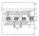
図1は、ウェハの前面1aに隣接したウェハの領域1dに、デバイスおよび数レベルの高密度相互接続配線11(通常Cu)を有する、ウェハ1の横断面図を示す。ウェハには金属化バイア12が形成されており、バイアはデバイスおよび横方向の相互接続の領域1dの下まで延在している。これらのバイアは、ウェハ1を薄くした後、垂直貫通接続の一部となるものである。バイア12は、一般に、ウェハ1に孔をエッチングし、孔の側部と底部にライナー材料の層を形成し、孔に金属(好ましくは銅)を充填することによって形成される。バイア12の深さは、薄くした後のウェハ1の最終的な厚みより小さい。したがって、薄くした後のウェハの厚みが約10μmの場合は、バイアの深さは10μm未満である。バイア12の直径は、熱伝導とスペースの問題をバランスさせるように選ばなければならない。約1μmの直径は、ウェハ表面上の最小限のスペースを消費し、かつウェハを通して許容できる熱伝導を提供する。より小さいバイア直径を用いることもできるが、垂直ウェハ・スタックを通して熱を伝導するには十分でない恐れがある。(1) Top-down Wafer Lamination Method FIG. 1 shows a cross section of a
説明の便宜上、バイア12は、ウェハ領域内へデバイス領域の下まで一定の径で真っ直ぐ下方へ延在しているように図示されている。バイアの寸法要件は、実際は、領域1dの下では実質的に緩和することができる。以下により詳しく説明するように、デバイスの真下に横方向に延在する貫通接続を伴うような、その他の配置も可能である。 For convenience of explanation, the via 12 is illustrated as extending straight down into the wafer area with a constant diameter down to the bottom of the device area. Via dimension requirements can actually be relaxed under
薄くしたウェハの取扱いを容易にするために、ウェハの前面1aにハンドリング・プレート(通常ガラス)15を取付ける。ウェハ1とプレート15は、熱可塑性接合材料、好ましくはポリイミドの層16を用いて接合する。 In order to facilitate handling of the thinned wafer, a handling plate (usually glass) 15 is attached to the
ハンドリング・プレート15をウェハ1に取付けた状態で、裏側1bを研削または研磨することによって、ウェハを薄くする(図2参照)。得られるウェハ1の厚みは、20μm未満、好ましくは約10μmである。図2に示すように、薄型化プロセスは、バイア12の底部を露出させる手前で止める。 With the handling
次いで、ウェハの裏面1bに開口13をエッチングして、バイア12の底部を露出させる(図3)。バイア内の金属自体が、このプロセスのエッチ・ストップとしての役割を果たすことができる。あるいは、ウェハの別の部分(デバイスが取付けられていない)にエッチ・ストップ層を形成してこのプロセスを制御させることもできる。開口13は、バイア12の開口より径が大きいことに留意されたい。数多くのバイアの配置が可能である(さらに以下に説明するように)が、一般に裏面1bの開口は、前面1aのバイアより大きい。 Next, the
次いで、開口13の内面14に(好ましくはスパッタリングによって)金属で覆って、対応するバイア12の底端部と接触させ、ウェハ1を貫通する導電経路を形成する。開口13の径が対応するバイア12の径より大きい(通常、2倍大きい)ことに留意されたい。これは、別のウェハとの垂直接続を容易にするためである。 The
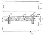
図4は、ウェハ1と垂直に集積されることになる第2のウェハを示す。ウェハ2には、ウェハ1と同様に、デバイスおよび相互接続配線21が形成されている。さらに、金属化バイア22(通常、銅を充填)がウェハ2内部下方へ延在している。バイア22は、表面2aで横方向寸法221を有する。ポリイミド層26を、ウェハ2の前面2aに付着させる。層26の上面を超えて、通常5μm以下の距離で延在するスタッド27を表面2aに形成する。スタッド27は、Ni、Cu、NiめっきCu、Wまたは他の金属、あるいは金属の組み合わせから形成することができる。低融点合金材料の層28を、スタッドの表面上に付着させる。これにより、ウェハ1と2を垂直に接合するプロセス時に電気接続の形成が容易になる。この合金材料は、通常、Pb/Sn90/10のはんだであり、厚みが2μm以下である。代わりの合金材料としては、Au/SnおよびSn/Agが挙げられる。合金材料に高温リフロー・プロセスを施して、図4に示したように、層28を丸型とすることができる。これにより、ウェハ1の対応する開口へのウェハ2のスタッドの整合が容易になる。スタッドは、電気接続をウェハ2のデバイスから垂直上方へ延長し、一方バイア22は、電気接続を垂直下方へ延長する。 FIG. 4 shows a second wafer to be integrated perpendicular to the
次いで、(ハンドリング・プレート15に取付けられた)ウェハ1を、ボンディング積層プロセスを用いて、ウェハ2に取付ける。図5に示したように、ウェハ2のスタッド27をウェハ1の開口13と位置合わせして、ウェハ1の裏面1bをポリイミド層26の前面と接触させる。積層プロセスは、(1)ウェハ1と層26とのボンディングを確保し、かつ(2)スタッド27と金属14との(したがってバイア12への)電気的接触を確保するのに十分な温度と圧力で行う。使用する材料に応じて、温度は200℃〜400℃の範囲とすることができ、圧力は10psi〜200psi(0.7kg/cm2〜14kg/cm2)とすることができる。図5に示したように、ボンディング積層プロセスでは、はんだ28が部分的または完全に開口13を満たすように、はんだ28を流動化させる。The wafer 1 (attached to the handling plate 15) is then attached to the
開口13の径はスタッド27より大きく、したがってウェハ1に対するウェハ2の横方向の位置の不正確さを吸収することができることに留意されたい。さらに、表面1bと2aは直接接触しているのではなく、その間に層26があることにも留意されたい。ポリイミド層26は、表面の小さな粒子を覆い、表面のわずかな欠陥を充填し、あるいは2つのウェハの平坦性の違いを吸収するのに十分な厚みを有している。したがって、層26は、ウェハ間の信頼できる機械的接合を確保するのに重要な役割を果たしている。一方、スタッド/バイア接続27−28−14−12は、信頼できる垂直の電気接続を形成する。 It should be noted that the diameter of the
次いで、ウェハ2(既にウェハ1に接合されている)を、20μm未満、好ましくは約10μmまで薄くする。図6に示したように、開口23をウェハ2の裏面2bに形成して、バイア22の底部を露出させる。開口23の内面は、別のウェハ3への電気接続を形成するために、金属24で(ウェハ1のように好ましくはスパッタリングによって)覆う。 The wafer 2 (already bonded to the wafer 1) is then thinned to less than 20 μm, preferably about 10 μm. As shown in FIG. 6, an
図7は、ウェハ1および2に接合するウェハ3の準備を示す。ウェハ3も、その前面近傍にデバイスおよび相互接続配線31を有する。ウェハ2の裏側と電気的に接触するために、ウェハ3の前面3aにスタッド37を形成する。それぞれウェハ2のスタッド27および合金材料28と同様に、スタッド37はその表面に合金材料38を有する。層26と同様に、ポリイミド層36を表面3aに付着させる。この図では、ウェハ3は接合すべき垂直スタックの最後のウェハである。したがって、ウェハ3は、薄くしない(スタックに機械的強度を与えるために)し、ウェハを貫通するバイアの必要もない。 FIG. 7 shows the preparation of
図8は、ウェハ3のボンディング積層プロセスの結果を示す。開口23を充填し、金属層24に接合する合金材料38の結果、スタッド37はバイア22と電気的に接触する。ウェハ1と2の間の層26と同様に、ポリイミド層36をウェハ2の表面2bに接合する。薄くしていないウェハ3が薄型ウェハ1および2に機械的強度を与えるので、ハンドリング・プレート15はもはや必要なく、この時点で取り外すことができる。これは、レーザ・アブレーションによって好都合に行うことができる。即ち、プレート15が剥離性放射線に透明の場合、レーザを用いてプレート15と層16の間を剥離させることにより、プレートを取り外すことができる。 FIG. 8 shows the result of the bonding lamination process of the
次いで、図9に示したように、垂直に相互接続したウェハ・スタック1−2−3に外部接続を取付けることができる。図9は、垂直スタックを、C4技術を用いてより大きなデバイスの他の部品に接続する例を示す。開口40を層16に形成して、ウェハ1の金属化バイア12を露出させる。次いで、金属パッド41を開口に付着させる。次いで、当技術分野で知られた(例えば)はんだマスク技術を用いて、C4はんだバンプ42をこれらのパッド上に形成する。これで、この完成した垂直集積デバイス100を、マルチチップ・モジュール(MCM)上のC4パッド等に接合する準備ができた。 Then, as shown in FIG. 9, external connections can be attached to the vertically interconnected wafer stack 1-2-3. FIG. 9 shows an example of connecting a vertical stack to other parts of a larger device using C4 technology.
ウェハ1、2および3の内部構造は概略的にしか図示されていないことに留意されたい。実際、これらのウェハは、様々な方法によって製造することができ、様々な機能を持つことができる。例えば、3つのウェハすべては、キャッシュ・メモリ装置を持つことができる。ウェハ1と2はメモリを持つことができ、ウェハ3は論理装置を持つことができる。ウェハの1つ以上はマイクロ電気機械システム(MEMS)を組み込むことができる。 Note that the internal structure of
本発明者等は、(1)ウェハを約10μmに薄くして、バイアでの垂直熱伝導の問題を最小化すること、(2)熱可塑性接合材料としてポリイミドを使って、ウェハの平坦性および清潔度要件を緩和すること、ならびに(3)裏側のバイア開口がスタッドより実質的に大きいスタッド/バイア接続を使って、横方向の位置合わせの要件を緩和すること、によって正常なウェハ・レベルの垂直集積が確保されることを見出した。 We (1) thin the wafer to about 10 μm to minimize the problem of vertical heat conduction in the vias, (2) use polyimide as the thermoplastic bonding material, Normal wafer level by relaxing cleanliness requirements and (3) relaxing lateral alignment requirements by using stud / via connections where the backside via opening is substantially larger than the stud We found that vertical accumulation is ensured.
(2)ボトムアップ式ウェハ積層プロセス
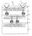
垂直スタックにウェハを接合する代替方法を図10〜14に示す。この方法を3つのウェハについて詳述するが、上記のように、より多いまたは少ないウェハにも適用することができる。図1〜3に示した方法で、まずウェハ1を作製する。したがって、このウェハは、約10μmに薄くされており、裏面に開口13を有する金属化バイア12を持ち、ポリアミド層16を有する前面にハンドリング・プレート15が取付けられている。(2) Bottom-up Wafer Lamination Process An alternative method for bonding wafers to a vertical stack is shown in FIGS. Although this method is described in detail for three wafers, it can be applied to more or fewer wafers as described above. First, a
次いで、図10に示したように、横方向相互接続配線51を有する第2のウェハ5を作製する。ウェハ5は、上記のプロセスにおけるウェハ2と同様に、バイア52および合金材料58を有するスタッド57を有する(図4と比較のこと)。ウェハ5にハンドリング・プレート55を設ける。プレート55は、スタッド57を収容するようにパターン化されたポリイミド・コーティング56で覆われている。次いで、ウェハ5をハンドリング・プレート55に接合する。これにより、ウェハを薄くすることができる(図11)。薄くしたウェハの裏側5bに開口53を形成し、上記のようにその内面を金属層54で覆う。 Next, as shown in FIG. 10, the
ウェハ1および5には、それぞれのハンドリング・プレート15および55があるので、各々個別に作製、接合および薄型化することができる。 Since
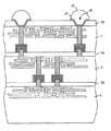
図12に示したように、横方向相互接続配線61を有する第3のウェハ6を作製する。この(図7に示したウェハ3と同様の)ウェハには、その前面上のポリイミド層66およびスタッド67があり、スタッド67はその表面に合金材料68を有し、他のウェハへの垂直電気接続を作る。スタッド67は、ウェハ5の金属層54と接触するのに十分な距離(即ち、約5μm)だけ層66から突き出ている。次いで、図13に示したように、ウェハ5と6を接合積層する。ウェハ6は薄くしていないので、ボンディング・プロセスの後ではハンドリング・プレート55は必要なく、したがって取り外される。この時点で、ウェハ5の前面5a上の層56の厚みを薄くしてスタッド57の高さを約5μm露出させる。ここで、スタッド57は、ウェハ1の金属層14へのボンディングの準備が整った。このボンディング・プロセスの結果、積層されたウェハ5と6がウェハ1に接合される。この結果を図14に示す。合金材料58が薄くしたウェハ1の開口13を充填し、金属層14と、したがってバイア12に電気的に接触する。ウェハ5と6をウェハ1に接合した後、ハンドリング・プレート15はもはや必要がなく、これを取り外して層16を露出させることができる。次いで、層16内に開口40を形成し、金属パッド41とC4はんだバンプ42を形成して、バイア12と接続する(図15;図9と比較されたい)。 As shown in FIG. 12, the
複数の薄型チップを積層し、チップからチップへの垂直相互接続を組み込む上記の技術により、その面積(2次元の)を大きくすることなく、チップの内容および機能が大きく増加することを理解されたい。これらのプロセスは、同じ内容を有するチップに特に魅力的である。この場合は、各薄型積層チップのサイズが同じであるからである。この結果、デバイスの加工全体が著しく単純化され、より経済的になる。これらのプロセスにより、ウェハ・レベルのチップとチップの相互接続が可能になるので、単一チップの垂直配置、ボンディングおよび相互接続プロセスと比べて、3Dチップを作るプロセスのコストが著しく低下する。上記の垂直相互接続方式とは異なり、本発明のチップとチップの相互接続は、チップの側部に沿って作られるのではなく、直接チップを貫通して形成される。 It should be understood that the above technique of stacking multiple thin chips and incorporating chip-to-chip vertical interconnects greatly increases chip content and function without increasing its area (two-dimensional). . These processes are particularly attractive for chips that have the same content. In this case, the size of each thin laminated chip is the same. As a result, the overall processing of the device is significantly simplified and more economical. These processes allow wafer level chip-to-chip interconnects, thus significantly reducing the cost of the process of making 3D chips compared to single chip vertical placement, bonding and interconnect processes. Unlike the vertical interconnect scheme described above, the chip-to-chip interconnection of the present invention is not made along the side of the chip, but directly through the chip.
積層ウェハの厚みが薄くなったこと(約10μm)により、各チップ間の相互接続長さ(例えば、キャッシュ・メモリ装置間の)が、こうしたチップの2D配置よりかなり短くなることは注目に値する。これにより、2次元面積が縮小すること以外に、デバイス性能が改良されるというメリットもある。 It is noteworthy that due to the reduced thickness of the laminated wafer (approximately 10 μm), the interconnect length between chips (eg, between cache memory devices) is significantly shorter than the 2D placement of such chips. Thereby, in addition to the reduction of the two-dimensional area, there is also an advantage that the device performance is improved.
図1〜9および10〜15では、説明の便宜上、バイアは、ウェハを通って一定の径で真っ直ぐ下方へ延在しているように図示されている。垂直のチップ間相互接続が、ウェハの全厚みを通して、あるいは薄型ウェハの総厚み10μmについてさえ、小さな直径を有する必要はない。例えば、図16示したように、ウェハ1は、その内部に大きな金属領域102を埋め込んで作製することもできる。この場合、垂直の相互接続は、ウェハのデバイス領域1dを通って延在する際にスペースを節約するための小径(1μm未満)の垂直配線12と、デバイス領域の真下に横方向に延在し、裏側の開口103の金属化された内面と接続する、より大きな金属領域102とを含む。したがって、開口103は、領域102の横方向の程度に応じて、バイア12から横方向に離れている。この配置は、デバイス領域における垂直相互接続に必要なスペースを最小にすると同時に、相互接続の抵抗を低下させる。さらに、この配置により、相互接続領域を、ウェハのデバイス領域のすぐ下に置くことができることに留意されたい(例えば、領域1dのすぐ下に位置する開口103を通って別のウェハへ相互接続する)。その結果、開口103のサイズと位置にフレキシビリティができ、したがってウェハ間(この例では、ウェハ1と2の間)を正確に位置合わせする必要性が緩和される。 In FIGS. 1-9 and 10-15, the vias are illustrated as extending straight down through the wafer with a constant diameter for convenience of explanation. The vertical chip-to-chip interconnect need not have a small diameter throughout the wafer thickness, or even for a total thickness of 10 μm for thin wafers. For example, as shown in FIG. 16, the
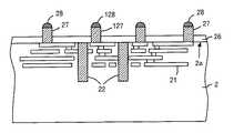
ウェハ間の金属化垂直接続は、電気信号だけでなく熱伝導にも使用することができる。例えば、図17に示したように、ウェハ1のデバイス領域の下を横方向に電気経路が通っており、ウェハ裏側1bの電気接続開口13の間に追加のスペースを形成している。開口13およびメタライゼーション14と同様に、追加の開口113をウェハ表面に形成し、その内面114を金属で覆う。(開口13、113は、同じプロセス工程で形成することができる。メタライゼーション14、114も同様である。)追加の開口113は、電気接続の一部を形成するものではなく、ウェハ・スタックを通る熱伝導の経路を提供する役割を果たす。図18に示したように、低融点合金材料128で覆われた追加のスタッド127を、ウェハ2の前面2a上に形成する。上記のプロセスで各ウェハを接合すると、スタッド127は、開口113の金属114と接続して、ウェハ1と2の間に金属化熱伝導経路を形成する(図19を参照されたい)。図19に示したように、スタッド127は、バイア22またはスタッド27と電気的に接続しても、しなくてもよい。どんな電気信号もウェハ1の前面に運ばれない。 Metallized vertical connections between wafers can be used not only for electrical signals but also for heat conduction. For example, as shown in FIG. 17, an electrical path runs laterally under the device region of the
図17〜19の熱伝導経路がウェハ1と2の間に形成されるとして図示されているが、この技術を用いて、上記のどの集積プロセスのスタックのどんなウェハの間(図8に示したウェハ2と3の間、図13に示したウェハ5と6の間など)の熱伝導も改良することができることを理解されたい。 Although the heat transfer paths of FIGS. 17-19 are illustrated as being formed between
図20は、横方向にチップ(例えば、論理装置)200と接続した垂直集積スタック(例えば、キャッシュ・メモリ装置)100を有するデバイス400を示す。マルチチップ・モジュール(MCM)300へはC4接続が用いられている。垂直メモリ・スタックおよび論理チップは、それぞれC4はんだバンプ42および242を有する。これらは、MCMのC4パッド301に接合されている。次いで、MCM300を、より大きな、より複雑なデバイスへ集積することができる。 FIG. 20 shows a
図21に示したように、スタッド/バイア接続を用いることにより、キャッシュ・メモリと論理装置の間のより密な接続を実現することができる。キャッシュ・メモリ装置401を、上記のプロセスの1つに従って作製するが、ここではポリイミド層411に金属化バイア420を有する(図9および15と比較されたい)。同様のバイアを、論理装置402のポリイミド層412に形成する。その内部に相互接続配線が埋め込まれた(低k誘電材料、酸化物、またはポリイミドからなる)絶縁層450の上には、バイアの位置と整合するようにスタッド422を形成する。層450をハンドリング・プレート(図示せず)上に構築し、次いで装置401および402をスタッド422と整合させることができる。スタッド422をバイアの金属パッド421と接続するボンディング・プロセスの後、ハンドリング・プレートを表面450bから取り外す。装置401と402の間のギャップ403は、機械強度を増すために適切な材料(例えば、ポリイミド)で充填することができる。次いで、結合されたデバイス(メモリ装置401、論理装置402、および相互接続層450を含む)は、このデバイスへの外部接続を作るために、表面450b上にC4パッド451およびC4はんだバンプ452を形成することができる。 As shown in FIG. 21, a tighter connection between the cache memory and the logic unit can be achieved by using a stud / via connection. The
別法として、キャッシュ・メモリと論理装置を組み込んだデバイスにおいて、図22に示したように、両者を垂直スタックに集積することもできる。結合されたデバイス500は、キャッシュ・メモリチップ501および502と集積された論理装置510を含む。この配置では、論理装置510はスタックの最表面にある。過剰の熱を除去するにはここが最も容易である。 Alternatively, in a device incorporating a cache memory and logic device, both can be integrated in a vertical stack as shown in FIG. The combined
図20〜22の装置100、200、401、402、500は、単に論理またはメモリ装置あるいはその両方である必要はなく、実際は多種多様なデバイスの内のどれでもよいことを理解されたい。したがって、本発明の方法を用いて、様々なデバイス技術を3D集積デバイスに容易に組み合わせることができる。 It should be understood that the
本発明は、高面積密度のデバイスが必要な半導体デバイス構造に一般に適用することができる。本発明は、特に、大きなメモリ・キャッシュ内容が必要なチップに適用することができる。このようなチップは、レチクルの大きさが限られていることにより、あるいはプロセス歩留まりが低いことにより、現在利用できる方法では製造することができない。 The present invention is generally applicable to semiconductor device structures that require high area density devices. The present invention is particularly applicable to chips that require large memory cache contents. Such a chip cannot be manufactured by currently available methods due to the limited size of the reticle or the low process yield.
具体的な実施形態について本発明を説明してきたが、上記の説明に鑑み、当分野の技術者には数多くの代替、修正および変形形態が明らかになることは明白である。したがって、本発明は、本発明および頭記の特許請求の範囲の、範囲および精神の中に入るこうした代替、修正および変形形態のすべてを包含するものとする。 While the invention has been described in terms of specific embodiments, it is evident that many alternatives, modifications and variations will become apparent to those skilled in the art in view of the foregoing description. Accordingly, the present invention is intended to embrace all such alternatives, modifications and variations that fall within the scope and spirit of the present invention and the appended claims.
Claims (4)
Translated fromJapanese前記第1のウェハに、前記前面から延在し、前記前面での横方向寸法(121)を特徴とするバイア(12)を形成するステップと、
前記第1のウェハから、前記ウェハ裏面(1b)の材料を除去するステップと、
前記第1のウェハの前記裏面に、前記バイアの前記横方向寸法より大きい横方向寸法を有する開口(13)を形成することにより、前記バイアを露出させるステップと、
前記開口に導電材料の層(14)を形成するステップと、
前面(2a)と裏面(2b)を有し、前記ウェハ前面に隣接した内部に形成されたデバイスを有する、第2のウェハ(2)を設けるステップと、
前記第2のウェハの前記前面にスタッド(27)を形成するステップと、
前記第2のウェハの前記前面(2a)に、前記スタッドがそこから垂直に突き出るように、接合材料の層(26)を形成するステップと、
前記第1のウェハの前記裏面の前記開口(13)に、前記スタッド(27)を位置合わせするステップと、
前記接合材料の層(26)を用いて前記第2のウェハを前記第1のウェハに接合して、前記スタッドを前記バイアと電気的に接触させるステップと
を含む方法であって、
前記第1のウェハの前記裏面に電気的接続の一部を形成しない追加の開口(113)を形成するステップと、
前記追加の開口に導電材料の追加の層(114)を形成するステップと、
前記第2のウェハの前記前面に追加のスタッド(127)を形成するステップと、
前記追加のスタッド(127)を、前記第1のウェハの前記裏面の前記追加の開口(113)に位置を合わせるステップと、
をさらに含み、
前記第2のウェハを前記第1のウェハに接合する前記ステップが、前記第2のウェハと前記第1のウェハとの間に熱を伝導するために、前記追加のスタッド(127)と前記導電材料の追加の層(114)との接続を形成することを特徴とする方法。A method for manufacturing a three-dimensional integrated device comprising a plurality of vertically stacked and interconnected wafers, comprising a front surface (1a) and a back surface (1b), formed in a region (1d) adjacent to the front surface of the wafer Providing a first wafer (1) having a suitable device;
Forming a via (12) in the first wafer extending from the front surface and characterized by a lateral dimension (121) at the front surface;
Removing the material of the wafer back surface (1b) from the first wafer;
Exposing the via by forming an opening (13) in the back surface of the first wafer having a lateral dimension greater than the lateral dimension of the via;
Forming a layer of conductive material (14) in the opening;
Providing a second wafer (2) having a front surface (2a) and a back surface (2b) and having devices formed therein adjacent to the wafer front surface;
Forming studs (27) on the front surface of the second wafer;
Forming a layer (26) of bonding material on the front surface (2a) of the second wafer such that the studs protrude vertically therefrom;
Aligning the stud (27) with the opening (13) on the back surface of the first wafer;
Bonding the second wafer to the first wafer using the layer of bonding material (26) to electrically contact the stud with the via,
Forming an additional opening (113) in the back surface of the first wafer that does not form part of an electrical connection;
Forming an additional layer (114) of conductive material in the additional opening;
Forming an additional stud (127) on the front surface of the second wafer;
Aligning the additional stud (127) with the additional opening (113) on the back surface of the first wafer;
Further including
The step of bonding the second wafer to the first wafer includes the additional stud (127) and the conductive material for conducting heat between the second wafer and the first wafer. how and forming a connection with the additional layer of material (114).
前面(1a)と裏面(1b)を有し、前記ウェハ前面に隣接した領域(1d)に形成されたデバイスを有する、第1のウェハ(1)を設けるステップと、
前記第1のウェハに、前記前面から延在し、前記前面での横方向寸法(121)を特徴とするバイア(12)を形成するステップと、
前記第1のウェハから、前記ウェハ裏面(1b)の材料を除去するステップと、
前記第1のウェハの前記裏面に、前記バイアの前記横方向寸法より大きい横方向寸法を有する開口(13)を形成することにより、前記バイアを露出させるステップと、
前記開口に導電材料の層(14)を形成するステップと、
前面(2a)と裏面(2b)を有し、前記ウェハ前面に隣接した内部に形成されたデバイスを有する、第2のウェハ(2)を設けるステップと、
前記第2のウェハの前記前面にスタッド(27)を形成するステップと、
前記第2のウェハの前記前面(2a)に、前記スタッドがそこから垂直に突き出るように、接合材料の層(26)を形成するステップと、
前記第1のウェハの前記裏面の前記開口(13)に、前記スタッド(27)を位置合わせするステップと、
前記接合材料の層(26)を用いて前記第2のウェハを前記第1のウェハに接合して、前記スタッドを前記バイアと電気的に接触させるステップと
を含む方法であって、
前記第2のウェハ(2)に、前記ウェハ前面(2a)から延在し、前記前面(2a)での横方向寸法(221)を特徴とするバイア(22)を形成するステップと、
前記第2のウェハから、前記ウェハ裏面(2b)の材料を除去するステップと、
前記第2のウェハの前記裏面(2b)に、前記バイア(22)の前記横方向寸法(221)より大きい横方向寸法を有する開口(23)を形成することにより、前記バイア(22)をその内部に露出させるステップと、
前記開口に導電材料の層(24)を形成するステップと、
前面(3a)を有し、前記ウェハ前面に隣接した内部に形成されたデバイスを有する、第3のウェハ(3)を設けるステップと、
前記第3のウェハの前記前面(3a)にスタッド(37)を形成するステップと、
前記第3のウェハの前記前面(3a)に、前記スタッドがそこから垂直に突き出るように、接合材料の層(36)を形成するステップと、
前記第2のウェハの前記裏面の前記開口(23)に、前記スタッド(37)を位置合わせするステップと、
前記接合材料の層(36)を用いて前記第3のウェハを前記第2のウェハに接合して、前記第3のウェハの前記スタッド(37)を、前記第2のウェハの前記バイア(22)、前記第2のウェハの前記スタッド(27)、および前記第1のウェハの前記バイア(12)と電気的に接触させるステップと
をさらに含み、
前記第1のウェハの前記裏面に電気的接続の一部を形成しない追加の開口(113)を形成するステップと、
前記追加の開口に導電材料の追加の層(114)を形成するステップと、
前記第2のウェハの前記前面に追加のスタッド(127)を形成するステップと、
前記追加のスタッド(127)を、前記第1のウェハの前記裏面の前記追加の開口(113)に位置を合わせるステップと、
をさらに含み、
前記第2のウェハを前記第1のウェハに接合する前記ステップが、前記第2のウェハと前記第1のウェハとの間に熱を伝導するために、前記追加のスタッド(127)と前記導電材料の追加の層(114)との接続を形成する方法。A method of manufacturing a three-dimensional integrated device comprising a plurality of vertically stacked and interconnected wafers, comprising:
Providing a first wafer (1) having a front surface (1a) and a back surface (1b) and having a device formed in a region (1d) adjacent to the front surface of the wafer;
Forming a via (12) in the first wafer extending from the front surface and characterized by a lateral dimension (121) at the front surface;
Removing the material of the wafer back surface (1b) from the first wafer;
Exposing the via by forming an opening (13) in the back surface of the first wafer having a lateral dimension greater than the lateral dimension of the via;
Forming a layer of conductive material (14) in the opening;
Providing a second wafer (2) having a front surface (2a) and a back surface (2b) and having devices formed therein adjacent to the wafer front surface;
Forming studs (27) on the front surface of the second wafer;
Forming a layer (26) of bonding material on the front surface (2a) of the second wafer such that the studs protrude vertically therefrom;
Aligning the stud (27) with the opening (13) on the back surface of the first wafer;
Bonding the second wafer to the first wafer using the layer of bonding material (26) to electrically contact the stud with the via,
Forming a via (22) in the second wafer (2) extending from the wafer front surface (2a) and characterized by a lateral dimension (221) at the front surface (2a);
Removing the material of the wafer back surface (2b) from the second wafer;
By forming an opening (23) in the back surface (2b) of the second wafer having a lateral dimension larger than the lateral dimension (221) of the via (22), the via (22) Step to expose inside,
Forming a layer (24) of conductive material in the opening;
Providing a third wafer (3) having a front surface (3a) and having devices formed therein adjacent to the wafer front surface;
Forming a stud (37) on the front surface (3a) of the third wafer;
Forming a layer (36) of bonding material on the front surface (3a) of the third wafer such that the studs protrude perpendicularly therefrom;
Aligning the stud (37) with the opening (23) on the back surface of the second wafer;
The third wafer is bonded to the second wafer using the layer of bonding material (36), and the stud (37) of the third wafer is bonded to the via (22 of the second wafer). ), Electrically contacting the stud (27) of the second wafer and the via (12) of the first wafer;
Further including
Forming an additional opening (113) in the back surface of the first wafer that does not form part of an electrical connection;
Forming an additional layer (114) of conductive material in the additional opening;
Forming an additional stud (127) on the front surface of the second wafer;
Aligning the additional stud (127) with the additional opening (113) on the back surface of the first wafer;
Further including
The step of bonding the second wafer to the first wafer includes the additional stud (127) and the conductive material for conducting heat between the second wafer and the first wafer. A methodof forming a connection with an additional layer (114) of material .
前記追加の開口に導電材料の追加の層を形成するステップと、
前記第3のウェハの前記前面に追加のスタッドを形成するステップと、
前記追加のスタッドを、前記第2のウェハの前記裏面の前記追加の開口に位置合わせするステップと、
をさらに含み、
前記第3のウェハを前記第2のウェハに接合する前記ステップが、前記第3のウェハと前記第2のウェハとの間に熱を伝導するために、前記追加のスタッドと前記導電材料の追加の層との接続を形成することを特徴とする、請求項2に記載の方法。Forming an additional opening in the back surface of the second waferthat does not form part of an electrical connection ;
Forming an additional layer of conductive material in the additional opening;
Forming additional studs on the front surface of the third wafer;
Aligning the additional stud with the additional opening in the back surface of the second wafer;
Further including
The step of bonding the third wafer to the second wafer adds the additional stud and the conductive material to conduct heat between the third wafer and the second wafer. 3. A method according to claim2 , characterized in that a connection with a layer of is formed.
Applications Claiming Priority (1)
| Application Number | Priority Date | Filing Date | Title |
|---|---|---|---|
| PCT/US2002/041181WO2004059720A1 (en) | 2002-12-20 | 2002-12-20 | Three-dimensional device fabrication method |
Publications (2)
| Publication Number | Publication Date |
|---|---|
| JP2006522461A JP2006522461A (en) | 2006-09-28 |
| JP4575782B2true JP4575782B2 (en) | 2010-11-04 |
Family
ID=32679941
Family Applications (1)
| Application Number | Title | Priority Date | Filing Date |
|---|---|---|---|
| JP2004563148AExpired - Fee RelatedJP4575782B2 (en) | 2002-12-20 | 2002-12-20 | Manufacturing method of three-dimensional device |
Country Status (9)
| Country | Link |
|---|---|
| EP (1) | EP1573799B1 (en) |
| JP (1) | JP4575782B2 (en) |
| CN (1) | CN100383936C (en) |
| AT (1) | ATE456860T1 (en) |
| AU (1) | AU2002368524A1 (en) |
| DE (1) | DE60235267D1 (en) |
| IL (1) | IL169264A0 (en) |
| TW (1) | TWI242249B (en) |
| WO (1) | WO2004059720A1 (en) |
Families Citing this family (51)
| Publication number | Priority date | Publication date | Assignee | Title |
|---|---|---|---|---|
| US20060249753A1 (en)* | 2005-05-09 | 2006-11-09 | Matrix Semiconductor, Inc. | High-density nonvolatile memory array fabricated at low temperature comprising semiconductor diodes |
| ATE459101T1 (en)* | 2004-08-20 | 2010-03-15 | Nxp Bv | METHOD FOR SEPARATING A THIN SEMICONDUCTOR CIRCUIT FROM ITS BASE |
| US7262495B2 (en)* | 2004-10-07 | 2007-08-28 | Hewlett-Packard Development Company, L.P. | 3D interconnect with protruding contacts |
| US7485968B2 (en)* | 2005-08-11 | 2009-02-03 | Ziptronix, Inc. | 3D IC method and device |
| JP2009505435A (en)* | 2005-08-31 | 2009-02-05 | インテル コーポレイション | Package with microprocessor and level 4 cache |
| US7723759B2 (en)* | 2005-10-24 | 2010-05-25 | Intel Corporation | Stacked wafer or die packaging with enhanced thermal and device performance |
| FR2894070B1 (en)* | 2005-11-30 | 2008-04-11 | 3D Plus Sa Sa | 3D ELECTRONIC MODULE |
| JP4797677B2 (en)* | 2006-02-14 | 2011-10-19 | 旭硝子株式会社 | Multi-chip device and manufacturing method thereof |
| US7344959B1 (en)* | 2006-07-25 | 2008-03-18 | International Business Machines Corporation | Metal filled through via structure for providing vertical wafer-to-wafer interconnection |
| US8032711B2 (en)* | 2006-12-22 | 2011-10-04 | Intel Corporation | Prefetching from dynamic random access memory to a static random access memory |
| GB2449853B (en) | 2007-06-04 | 2012-02-08 | Detection Technology Oy | Photodetector for imaging system |
| JP5570689B2 (en)* | 2007-07-23 | 2014-08-13 | ピーエスフォー ルクスコ エスエイアールエル | Stacked memory |
| EP2075828A1 (en) | 2007-12-27 | 2009-07-01 | Interuniversitair Microelektronica Centrum (IMEC) | Semiconductor device and a method for aligining and bonding a first and second element for the fabrication of a semiconductor device |
| US8486823B2 (en)* | 2008-03-07 | 2013-07-16 | Taiwan Semiconductor Manufacturing Co., Ltd. | Methods of forming through via |
| US9136259B2 (en)* | 2008-04-11 | 2015-09-15 | Micron Technology, Inc. | Method of creating alignment/centering guides for small diameter, high density through-wafer via die stacking |
| US7821107B2 (en) | 2008-04-22 | 2010-10-26 | Micron Technology, Inc. | Die stacking with an annular via having a recessed socket |
| US8853830B2 (en)* | 2008-05-14 | 2014-10-07 | Taiwan Semiconductor Manufacturing Company, Ltd. | System, structure, and method of manufacturing a semiconductor substrate stack |
| WO2009146588A1 (en)* | 2008-06-05 | 2009-12-10 | Hong Kong Applied Science And Technology Research Institute Co., Ltd.. | Bonding method for through-silicon-via based 3d wafer stacking |
| JP4911143B2 (en) | 2008-08-15 | 2012-04-04 | 信越化学工業株式会社 | High temperature resistant adhesive composition, substrate bonding method, and three-dimensional semiconductor device |
| JP4947316B2 (en) | 2008-08-15 | 2012-06-06 | 信越化学工業株式会社 | Substrate bonding method and three-dimensional semiconductor device |
| US8129256B2 (en) | 2008-08-19 | 2012-03-06 | International Business Machines Corporation | 3D integrated circuit device fabrication with precisely controllable substrate removal |
| DE102009004725A1 (en)* | 2009-01-15 | 2010-07-29 | Austriamicrosystems Ag | Through-hole semiconductor circuit and method of manufacturing vertically integrated circuits |
| TWI402941B (en)* | 2009-12-03 | 2013-07-21 | Advanced Semiconductor Eng | Semiconductor structure and method for making the same |
| CN102683265A (en)* | 2011-03-15 | 2012-09-19 | 中国科学院微电子研究所 | Method for filling carbon nanotube bundle into through silicon via of silicon adapter plate |
| GB201108425D0 (en) | 2011-05-19 | 2011-07-06 | Zarlink Semiconductor Inc | Integrated circuit package |
| US8829684B2 (en) | 2011-05-19 | 2014-09-09 | Microsemi Semiconductor Limited | Integrated circuit package |
| EP2717300B1 (en) | 2011-05-24 | 2020-03-18 | Sony Corporation | Semiconductor device |
| JP2013042052A (en)* | 2011-08-19 | 2013-02-28 | Nec Corp | Manufacturing method for semiconductor device |
| JP2013098514A (en)* | 2011-11-07 | 2013-05-20 | Seiko Epson Corp | Semiconductor device manufacturing method, semiconductor device and electronic apparatus |
| JP2013201240A (en)* | 2012-03-23 | 2013-10-03 | Toshiba Corp | Method for manufacturing semiconductor device and glass substrate for semiconductor substrate support |
| TWI540710B (en) | 2012-06-22 | 2016-07-01 | Sony Corp | A semiconductor device, a method for manufacturing a semiconductor device, and an electronic device |
| TWI487041B (en)* | 2012-08-08 | 2015-06-01 | Subtron Technology Co Ltd | Package carrier board and manufacturing method thereof |
| CN103107128B (en)* | 2013-01-14 | 2014-12-17 | 武汉新芯集成电路制造有限公司 | Metal bonding method of three-dimensional chip structure and bonding structure |
| JP2014170793A (en)* | 2013-03-01 | 2014-09-18 | Fujitsu Semiconductor Ltd | Semiconductor device, semiconductor device manufacturing method and electronic apparatus |
| JP5939184B2 (en) | 2013-03-22 | 2016-06-22 | ソニー株式会社 | Manufacturing method of semiconductor device |
| US9136233B2 (en) | 2013-06-06 | 2015-09-15 | STMicroelctronis (Crolles 2) SAS | Process for fabricating a three-dimensional integrated structure with improved heat dissipation, and corresponding three-dimensional integrated structure |
| CN104008998B (en)* | 2014-06-10 | 2016-08-03 | 山东华芯半导体有限公司 | Multi-chip laminating method for packing |
| KR20170018815A (en)* | 2014-06-16 | 2017-02-20 | 인텔 코포레이션 | Embedded memory in interconnect stack on silicon die |
| US9633917B2 (en)* | 2015-08-20 | 2017-04-25 | Taiwan Semiconductor Manufacturing Co., Ltd. | Three dimensional integrated circuit structure and method of manufacturing the same |
| CN107994043A (en)* | 2017-12-11 | 2018-05-04 | 德淮半导体有限公司 | Wafer, stacked semiconductor devices and its manufacture method |
| CN109727848B (en)* | 2018-12-29 | 2020-09-01 | 长江存储科技有限责任公司 | A method of manufacturing a three-dimensional memory |
| CN109923668A (en) | 2019-01-30 | 2019-06-21 | 长江存储科技有限责任公司 | Use the hybrid bonded of illusory bonding contacts |
| KR102618755B1 (en) | 2019-01-30 | 2023-12-27 | 양쯔 메모리 테크놀로지스 씨오., 엘티디. | Hybrid bonding using dummy bonded contacts and dummy interconnects |
| US11545435B2 (en)* | 2019-06-10 | 2023-01-03 | Qualcomm Incorporated | Double sided embedded trace substrate |
| US12424543B2 (en)* | 2019-11-26 | 2025-09-23 | Intel Corporation | Selective interconnects in back-end-of-line metallization stacks of integrated circuitry |
| CN111106022A (en)* | 2019-12-30 | 2020-05-05 | 武汉新芯集成电路制造有限公司 | Bonding structure and manufacturing method thereof |
| US11581281B2 (en)* | 2020-06-26 | 2023-02-14 | Taiwan Semiconductor Manufacturing Co., Ltd. | Packaged semiconductor device and method of forming thereof |
| CN113990833A (en)* | 2021-09-15 | 2022-01-28 | 日月光半导体制造股份有限公司 | Conductive line structure and forming method thereof |
| US12394739B2 (en) | 2022-01-12 | 2025-08-19 | Changxin Memory Technologies, Inc. | Semiconductor package and method of manufacturing semiconductor package |
| CN116469857A (en)* | 2022-01-12 | 2023-07-21 | 长鑫存储技术有限公司 | Semiconductor structure and manufacturing method thereof |
| US12040296B2 (en) | 2022-01-12 | 2024-07-16 | Changxin Memory Technologies, Inc. | Semiconductor structure and method for manufacturing semiconductor structure |
Family Cites Families (30)
| Publication number | Priority date | Publication date | Assignee | Title |
|---|---|---|---|---|
| DE1514818A1 (en)* | 1951-01-28 | 1969-05-08 | Telefunken Patent | Solid-state circuit, consisting of a semiconductor body with inserted active components and an insulating layer with applied passive components and conductor tracks |
| JPS60140850A (en)* | 1983-12-28 | 1985-07-25 | Hitachi Ltd | Manufacturing method of stacked integrated semiconductor circuit device |
| JPS60160645A (en)* | 1984-02-01 | 1985-08-22 | Hitachi Ltd | Laminated semiconductor integrated circuit device |
| JPS62117316A (en)* | 1985-11-16 | 1987-05-28 | Sharp Corp | semiconductor equipment |
| KR900008647B1 (en)* | 1986-03-20 | 1990-11-26 | 후지쓰 가부시끼가이샤 | A method for manufacturing three demensional i.c. |
| JPS63142663A (en)* | 1986-12-04 | 1988-06-15 | Sharp Corp | Semiconductor device and its manufacturing method |
| US4982266A (en)* | 1987-12-23 | 1991-01-01 | Texas Instruments Incorporated | Integrated circuit with metal interconnecting layers above and below active circuitry |
| US4889832A (en)* | 1987-12-23 | 1989-12-26 | Texas Instruments Incorporated | Method of fabricating an integrated circuit with metal interconnecting layers above and below active circuitry |
| US5091331A (en)* | 1990-04-16 | 1992-02-25 | Harris Corporation | Ultra-thin circuit fabrication by controlled wafer debonding |
| US5376561A (en)* | 1990-12-31 | 1994-12-27 | Kopin Corporation | High density electronic circuit modules |
| US5229647A (en)* | 1991-03-27 | 1993-07-20 | Micron Technology, Inc. | High density data storage using stacked wafers |
| JPH0555534A (en)* | 1991-08-22 | 1993-03-05 | Seiko Instr Inc | Production of laminated semiconductor device |
| US5268326A (en)* | 1992-09-28 | 1993-12-07 | Motorola, Inc. | Method of making dielectric and conductive isolated island |
| US5426072A (en)* | 1993-01-21 | 1995-06-20 | Hughes Aircraft Company | Process of manufacturing a three dimensional integrated circuit from stacked SOI wafers using a temporary silicon substrate |
| EP0721662A1 (en)* | 1993-09-30 | 1996-07-17 | Kopin Corporation | Three-dimensional processor using transferred thin film circuits |
| US5424245A (en)* | 1994-01-04 | 1995-06-13 | Motorola, Inc. | Method of forming vias through two-sided substrate |
| US5627106A (en)* | 1994-05-06 | 1997-05-06 | United Microelectronics Corporation | Trench method for three dimensional chip connecting during IC fabrication |
| US5814889A (en)* | 1995-06-05 | 1998-09-29 | Harris Corporation | Intergrated circuit with coaxial isolation and method |
| US5807783A (en)* | 1996-10-07 | 1998-09-15 | Harris Corporation | Surface mount die by handle replacement |
| US5786238A (en)* | 1997-02-13 | 1998-07-28 | Generyal Dynamics Information Systems, Inc. | Laminated multilayer substrates |
| JP2897827B2 (en)* | 1997-04-08 | 1999-05-31 | 日本電気株式会社 | Multilayer wiring structure of semiconductor device |
| JP4032454B2 (en)* | 1997-06-27 | 2008-01-16 | ソニー株式会社 | Manufacturing method of three-dimensional circuit element |
| JP4063944B2 (en)* | 1998-03-13 | 2008-03-19 | 独立行政法人科学技術振興機構 | Manufacturing method of three-dimensional semiconductor integrated circuit device |
| US6093969A (en)* | 1999-05-15 | 2000-07-25 | Lin; Paul T. | Face-to-face (FTF) stacked assembly of substrate-on-bare-chip (SOBC) modules |
| JP4123682B2 (en)* | 2000-05-16 | 2008-07-23 | セイコーエプソン株式会社 | Semiconductor device and manufacturing method thereof |
| JP2001326325A (en)* | 2000-05-16 | 2001-11-22 | Seiko Epson Corp | Semiconductor device and manufacturing method thereof |
| JP3951091B2 (en)* | 2000-08-04 | 2007-08-01 | セイコーエプソン株式会社 | Manufacturing method of semiconductor device |
| US6444560B1 (en)* | 2000-09-26 | 2002-09-03 | International Business Machines Corporation | Process for making fine pitch connections between devices and structure made by the process |
| JP4560958B2 (en)* | 2000-12-21 | 2010-10-13 | 日本テキサス・インスツルメンツ株式会社 | Micro electro mechanical system |
| US6489217B1 (en)* | 2001-07-03 | 2002-12-03 | Maxim Integrated Products, Inc. | Method of forming an integrated circuit on a low loss substrate |
- 2002
- 2002-12-20WOPCT/US2002/041181patent/WO2004059720A1/enactiveApplication Filing
- 2002-12-20CNCNB028300335Apatent/CN100383936C/ennot_activeExpired - Fee Related
- 2002-12-20AUAU2002368524Apatent/AU2002368524A1/ennot_activeAbandoned
- 2002-12-20DEDE60235267Tpatent/DE60235267D1/ennot_activeExpired - Lifetime
- 2002-12-20JPJP2004563148Apatent/JP4575782B2/ennot_activeExpired - Fee Related
- 2002-12-20ATAT02808338Tpatent/ATE456860T1/ennot_activeIP Right Cessation
- 2002-12-20EPEP02808338Apatent/EP1573799B1/ennot_activeExpired - Lifetime
- 2003
- 2003-12-02TWTW092133840Apatent/TWI242249B/ennot_activeIP Right Cessation
- 2005
- 2005-06-19ILIL169264Apatent/IL169264A0/enunknown
Also Published As
| Publication number | Publication date |
|---|---|
| WO2004059720A1 (en) | 2004-07-15 |
| EP1573799B1 (en) | 2010-01-27 |
| TW200520108A (en) | 2005-06-16 |
| CN1708840A (en) | 2005-12-14 |
| IL169264A0 (en) | 2007-07-04 |
| CN100383936C (en) | 2008-04-23 |
| ATE456860T1 (en) | 2010-02-15 |
| EP1573799A4 (en) | 2009-02-25 |
| TWI242249B (en) | 2005-10-21 |
| AU2002368524A1 (en) | 2004-07-22 |
| DE60235267D1 (en) | 2010-03-18 |
| JP2006522461A (en) | 2006-09-28 |
| EP1573799A1 (en) | 2005-09-14 |
Similar Documents
| Publication | Publication Date | Title |
|---|---|---|
| JP4575782B2 (en) | Manufacturing method of three-dimensional device | |
| US7354798B2 (en) | Three-dimensional device fabrication method | |
| US6864165B1 (en) | Method of fabricating integrated electronic chip with an interconnect device | |
| JP4366510B2 (en) | Chip and wafer integration method using vertical connection part | |
| CN101752270B (en) | Method for forming semiconductor dies of stacked integrated circuits | |
| US7247518B2 (en) | Semiconductor device and method for manufacturing same | |
| US10446526B2 (en) | Face-to-face semiconductor assembly having semiconductor device in dielectric recess | |
| US8928123B2 (en) | Through via structure including a conductive portion and aligned solder portion | |
| JP4028211B2 (en) | Semiconductor device | |
| TWI854732B (en) | Interconnecting structure with high aspect ratio tsv and method for forming the same | |
| KR100621960B1 (en) | 3D device manufacturing method | |
| TWI611530B (en) | Thermally enhanced face-to-face semiconductor assembly with heat spreader and method of making the same | |
| CN118983269A (en) | A stacked chip packaging method | |
| CN119890152A (en) | Three-dimensional packaging chip and manufacturing method thereof |
Legal Events
| Date | Code | Title | Description |
|---|---|---|---|
| RD03 | Notification of appointment of power of attorney | Free format text:JAPANESE INTERMEDIATE CODE: A7423 Effective date:20090206 | |
| A131 | Notification of reasons for refusal | Free format text:JAPANESE INTERMEDIATE CODE: A131 Effective date:20091215 | |
| A521 | Request for written amendment filed | Free format text:JAPANESE INTERMEDIATE CODE: A523 Effective date:20100315 | |
| TRDD | Decision of grant or rejection written | ||
| A01 | Written decision to grant a patent or to grant a registration (utility model) | Free format text:JAPANESE INTERMEDIATE CODE: A01 Effective date:20100817 | |
| A01 | Written decision to grant a patent or to grant a registration (utility model) | Free format text:JAPANESE INTERMEDIATE CODE: A01 | |
| A61 | First payment of annual fees (during grant procedure) | Free format text:JAPANESE INTERMEDIATE CODE: A61 Effective date:20100820 | |
| R150 | Certificate of patent or registration of utility model | Free format text:JAPANESE INTERMEDIATE CODE: R150 | |
| FPAY | Renewal fee payment (event date is renewal date of database) | Free format text:PAYMENT UNTIL: 20130827 Year of fee payment:3 | |
| LAPS | Cancellation because of no payment of annual fees |